JP5400259B2 - Semiconductor memory device - Google Patents
Semiconductor memory device Download PDFInfo
- Publication number
- JP5400259B2 JP5400259B2 JP2005172077A JP2005172077A JP5400259B2 JP 5400259 B2 JP5400259 B2 JP 5400259B2 JP 2005172077 A JP2005172077 A JP 2005172077A JP 2005172077 A JP2005172077 A JP 2005172077A JP 5400259 B2 JP5400259 B2 JP 5400259B2
- Authority
- JP
- Japan
- Prior art keywords
- voltage
- line
- plate
- memory device
- bit line
- Prior art date
- Legal status (The legal status is an assumption and is not a legal conclusion. Google has not performed a legal analysis and makes no representation as to the accuracy of the status listed.)
- Expired - Fee Related
Links
Images


Classifications
-
- G—PHYSICS
- G11—INFORMATION STORAGE
- G11C—STATIC STORES
- G11C11/00—Digital stores characterised by the use of particular electric or magnetic storage elements; Storage elements therefor
- G11C11/21—Digital stores characterised by the use of particular electric or magnetic storage elements; Storage elements therefor using electric elements
- G11C11/34—Digital stores characterised by the use of particular electric or magnetic storage elements; Storage elements therefor using electric elements using semiconductor devices
- G11C11/40—Digital stores characterised by the use of particular electric or magnetic storage elements; Storage elements therefor using electric elements using semiconductor devices using transistors
- G11C11/401—Digital stores characterised by the use of particular electric or magnetic storage elements; Storage elements therefor using electric elements using semiconductor devices using transistors forming cells needing refreshing or charge regeneration, i.e. dynamic cells
- G11C11/4063—Auxiliary circuits, e.g. for addressing, decoding, driving, writing, sensing or timing
- G11C11/407—Auxiliary circuits, e.g. for addressing, decoding, driving, writing, sensing or timing for memory cells of the field-effect type
- G11C11/409—Read-write [R-W] circuits
- G11C11/4094—Bit-line management or control circuits
-
- G—PHYSICS
- G11—INFORMATION STORAGE
- G11C—STATIC STORES
- G11C11/00—Digital stores characterised by the use of particular electric or magnetic storage elements; Storage elements therefor
- G11C11/21—Digital stores characterised by the use of particular electric or magnetic storage elements; Storage elements therefor using electric elements
- G11C11/34—Digital stores characterised by the use of particular electric or magnetic storage elements; Storage elements therefor using electric elements using semiconductor devices
- G11C11/40—Digital stores characterised by the use of particular electric or magnetic storage elements; Storage elements therefor using electric elements using semiconductor devices using transistors
- G11C11/401—Digital stores characterised by the use of particular electric or magnetic storage elements; Storage elements therefor using electric elements using semiconductor devices using transistors forming cells needing refreshing or charge regeneration, i.e. dynamic cells
- G11C11/4063—Auxiliary circuits, e.g. for addressing, decoding, driving, writing, sensing or timing
- G11C11/407—Auxiliary circuits, e.g. for addressing, decoding, driving, writing, sensing or timing for memory cells of the field-effect type
- G11C11/4074—Power supply or voltage generation circuits, e.g. bias voltage generators, substrate voltage generators, back-up power, power control circuits
-
- G—PHYSICS
- G11—INFORMATION STORAGE
- G11C—STATIC STORES
- G11C11/00—Digital stores characterised by the use of particular electric or magnetic storage elements; Storage elements therefor
- G11C11/21—Digital stores characterised by the use of particular electric or magnetic storage elements; Storage elements therefor using electric elements
- G11C11/34—Digital stores characterised by the use of particular electric or magnetic storage elements; Storage elements therefor using electric elements using semiconductor devices
- G11C11/40—Digital stores characterised by the use of particular electric or magnetic storage elements; Storage elements therefor using electric elements using semiconductor devices using transistors
- G11C11/401—Digital stores characterised by the use of particular electric or magnetic storage elements; Storage elements therefor using electric elements using semiconductor devices using transistors forming cells needing refreshing or charge regeneration, i.e. dynamic cells
- G11C11/4063—Auxiliary circuits, e.g. for addressing, decoding, driving, writing, sensing or timing
- G11C11/407—Auxiliary circuits, e.g. for addressing, decoding, driving, writing, sensing or timing for memory cells of the field-effect type
- G11C11/409—Read-write [R-W] circuits
- G11C11/4097—Bit-line organisation, e.g. bit-line layout, folded bit lines
-
- G—PHYSICS
- G11—INFORMATION STORAGE
- G11C—STATIC STORES
- G11C7/00—Arrangements for writing information into, or reading information out from, a digital store
- G11C7/12—Bit line control circuits, e.g. drivers, boosters, pull-up circuits, pull-down circuits, precharging circuits, equalising circuits, for bit lines
-
- G—PHYSICS
- G11—INFORMATION STORAGE
- G11C—STATIC STORES
- G11C7/00—Arrangements for writing information into, or reading information out from, a digital store
- G11C7/18—Bit line organisation; Bit line lay-out
-
- H—ELECTRICITY
- H01—ELECTRIC ELEMENTS
- H01L—SEMICONDUCTOR DEVICES NOT COVERED BY CLASS H10
- H01L27/00—Devices consisting of a plurality of semiconductor or other solid-state components formed in or on a common substrate
- H01L27/02—Devices consisting of a plurality of semiconductor or other solid-state components formed in or on a common substrate including semiconductor components specially adapted for rectifying, oscillating, amplifying or switching and having at least one potential-jump barrier or surface barrier; including integrated passive circuit elements with at least one potential-jump barrier or surface barrier
- H01L27/0203—Particular design considerations for integrated circuits
- H01L27/0207—Geometrical layout of the components, e.g. computer aided design; custom LSI, semi-custom LSI, standard cell technique
-
- H—ELECTRICITY
- H10—SEMICONDUCTOR DEVICES; ELECTRIC SOLID-STATE DEVICES NOT OTHERWISE PROVIDED FOR
- H10B—ELECTRONIC MEMORY DEVICES
- H10B12/00—Dynamic random access memory [DRAM] devices
- H10B12/30—DRAM devices comprising one-transistor - one-capacitor [1T-1C] memory cells
- H10B12/48—Data lines or contacts therefor
-
- G—PHYSICS
- G11—INFORMATION STORAGE
- G11C—STATIC STORES
- G11C2211/00—Indexing scheme relating to digital stores characterized by the use of particular electric or magnetic storage elements; Storage elements therefor
- G11C2211/401—Indexing scheme relating to cells needing refreshing or charge regeneration, i.e. dynamic cells
- G11C2211/4013—Memory devices with multiple cells per bit, e.g. twin-cells
Description
本発明は、ダイナミック型ランダムアクセスメモリ(DRAM)などの半導体記憶装置に関し、特にプレート電極を駆動してメモリセルへの書き込み電荷量を増加する半導体記憶装置に適用して有効な技術に関するものである。 The present invention relates to a semiconductor memory device such as a dynamic random access memory (DRAM), and more particularly to a technique that is effective when applied to a semiconductor memory device that drives a plate electrode to increase the amount of charge written to a memory cell. .
本発明者が検討したところによれば、DRAMの微細化技術に関しては、以下のようなものが考えられる。 According to a study by the present inventor, the following can be considered as a technique for miniaturizing DRAM.
DRAMのメモリセルを微細化し高集積化するためには、限られたメモリセル底面積の中で大きな容量を実現するキャパシタおよび、微細トランジスタが必要である。メモリセルトランジスタを微細化する際に大きな問題となるのが、ゲート酸化膜の薄膜化である。MOSトランジスタのゲート長を短縮する際には、短チャネル効果を抑制するために、ゲート酸化膜を薄膜化する必要がある。 In order to miniaturize and highly integrate a DRAM memory cell, a capacitor and a fine transistor that realize a large capacity within a limited memory cell bottom area are required. A major problem when miniaturizing a memory cell transistor is thinning the gate oxide film. When shortening the gate length of the MOS transistor, it is necessary to reduce the thickness of the gate oxide film in order to suppress the short channel effect.
しかしながら、DRAMにおいては、メモリセルにNチャネルMOSトランジスタを用いており、蓄積ノードへの‘H’側の最大書込み電圧が、メモリセルトランジスタのゲートに印加されるワード線‘H’側の電圧VPPからしきい値電圧VT分下がったVPP−VTとなること、およびデータ保持特性を維持するためにしきい値電圧VTを低減することは許されないことから、ワード線電圧を容易には低減できない。したがって、ロジック製品に用いられるMOSトランジスタと比較すると、メモリセルトランジスタのゲート酸化膜は厚くなるため、微細化が困難である。 However, in the DRAM, an N-channel MOS transistor is used for the memory cell, and the maximum write voltage on the “H” side to the storage node is the voltage VPP on the word line “H” side applied to the gate of the memory cell transistor. Therefore, it is not allowed to reduce the threshold voltage VT in order to maintain VPP-VT that is lower than the threshold voltage VT from the threshold voltage, and to maintain the data retention characteristics, so the word line voltage cannot be easily reduced. Therefore, the gate oxide film of the memory cell transistor becomes thicker than a MOS transistor used in a logic product, and it is difficult to miniaturize it.
このような問題に対して、例えば特許文献1には、メモリセルのプレート電極を駆動して、メモリセルへの書込み電圧を高めるDRAMが示されている。本方式では、ワード線の‘H’側の電圧を低減して、これによって‘H’側データの書き込みが不十分になる問題を、プレート電極を駆動することにより補っている。このようにすると、メモリセルトランジスタのゲート酸化膜を薄膜化できるため、メモリセルを微細化することが可能になる。
ところで、前記のようなDRAMの微細化技術について、本発明者が検討した結果、以下のようなことが明らかとなった。 By the way, as a result of the study of the above-described DRAM miniaturization technology, the following has been clarified.
例えば、前述した特許文献1の技術には、次のような問題があることが判明した。メモリセルに用いる微細トランジスタは、しきい値電圧VTのばらつきが大きく、大容量のDRAMにおいては、ばらつきの範囲は1V近くになる。このようにメモリセルのしきい値電圧ばらつきが大きい場合にプレート駆動を行うと、メモリセルに書き込まれる電圧が大きなばらつきを持つ。すなわち、しきい値電圧が大きいセルに対して十分に電圧を書き込もうとして、プレートの振幅を大きくすると、しきい値電圧が小さいセルでは過剰に高い電圧が書き込まれてしまい、メモリセルトランジスタの信頼性が低下する。
For example, it has been found that the technique of
この問題を図20,図21を用いて説明する。図20は、本発明の前提として検討とした技術の半導体記憶装置において、プレートを駆動するDRAMメモリアレーの一部の構成例を示す回路図である。図21は、図20の半導体記憶装置において、その動作の一例を示す動作波形図である。 This problem will be described with reference to FIGS. FIG. 20 is a circuit diagram showing a configuration example of a part of a DRAM memory array for driving a plate in the semiconductor memory device of the technology studied as a premise of the present invention. FIG. 21 is an operation waveform diagram showing an example of the operation of the semiconductor memory device of FIG.
図20に示すDRAMメモリアレーは、例えば、メインワード線MWLBやサブワードドライバ選択線FXによって駆動されるワード線WL0と、ビット線BLT,BLBと、ワード線WL0とビット線BLTの交点に設けられたメモリセルと、ビット線BLT,BLB間に設けられたセンスアンプSAなどを含んでいる。メモリセルは、メモリセルトランジスタとキャパシタCsを含んでおり、キャパシタCsの一端(メモリセルトランジスタ側)は蓄積ノードSNであり、他端はプレート線PLである。 The DRAM memory array shown in FIG. 20 is provided at the intersection of the word line WL0 driven by the main word line MWLB and the sub word driver selection line FX, the bit lines BLT and BLB, and the word line WL0 and the bit line BLT, for example. It includes a memory cell and a sense amplifier SA provided between the bit lines BLT and BLB. The memory cell includes a memory cell transistor and a capacitor Cs. One end (on the memory cell transistor side) of the capacitor Cs is the storage node SN, and the other end is the plate line PL.
センスアンプSAは、センスアンプ分離信号SHR0,SHR1によって駆動されるトランスファーゲートTGCと、列選択線YSによってビット線BLT,BLBとローカルIO線対(LIO線対)を接続する読み出し・書き込みポートIOPと、プリチャージ信号BLEQの活性化によってビット線BLT,BLBのプリチャージを行うプリチャージ回路PCCと、P側共通ソース線CSPおよびN側共通ソース線CSNの駆動によってビット線BLT,BLBの電圧差を増幅するクロスカップル・アンプCCとを含んでいる。なお、ここでは一部の構成を示しているが、実際のDRAMメモリアレーには、多数のメモリセルやセンスアンプSA等が含まれる。 The sense amplifier SA includes a transfer gate TGC driven by sense amplifier isolation signals SHR0 and SHR1, and a read / write port IOP that connects the bit lines BLT and BLB to a local IO line pair (LIO line pair) by a column selection line YS. The precharge circuit PCC that precharges the bit lines BLT and BLB by activating the precharge signal BLEQ, and the voltage difference between the bit lines BLT and BLB by driving the P-side common source line CSP and the N-side common source line CSN. It includes a cross-coupled amplifier CC that amplifies. Although a partial configuration is shown here, an actual DRAM memory array includes a large number of memory cells, sense amplifiers SA, and the like.
このような構成に対し、例えば図21のような動作が行われる。まず、チップ外部からバンク活性化コマンドACTが入力されると、アドレスで指定されたセンスアンプSAにおいてセンスアンプ分離信号SHRの片側SHR1とプリチャージ信号BLEQが非活性化される。行デコーダにおいて、メインワード線MWLBがVKKに下がり、アレー制御回路においてサブワードドライバ選択線FXが活性化されると、選択されたワード線WL0がVKKからVPPに活性化される。ここで、VKKは負電源発生回路により発生されたワード線の低レベル側の電源電圧であり、VPPは高レベル側の電源電圧である。 For example, an operation as shown in FIG. 21 is performed for such a configuration. First, when a bank activation command ACT is input from the outside of the chip, one side SHR1 of the sense amplifier isolation signal SHR and the precharge signal BLEQ are deactivated in the sense amplifier SA designated by the address. In the row decoder, when the main word line MWLB falls to VKK and the sub word driver selection line FX is activated in the array control circuit, the selected word line WL0 is activated from VKK to VPP. Here, VKK is a power supply voltage on the low level side of the word line generated by the negative power supply generation circuit, and VPP is a power supply voltage on the high level side.
そして、ワード線WL0によって選択されたメモリセルにおいては、メモリセルトランジスタが導通し、ビット線BLT上に信号が読み出される。図21では、メモリセルに接地電圧VSSが書き込まれており、‘L’の信号が発生した例を示している。その後、センスアンプSAにおいてP側共通ソース線CSPがVDLに、N側共通ソース線CSNが接地電圧VSSに駆動され、ビット線BLT,BLB上の信号が増幅される。この状態で、メモリチップは、リードコマンドRDまたはライトコマンドWRTを受け付けることができる。図21では、ライトコマンドWRTが入力された場合を示している。 In the memory cell selected by the word line WL0, the memory cell transistor is turned on, and a signal is read onto the bit line BLT. FIG. 21 shows an example in which the ground voltage VSS is written in the memory cell and a signal of “L” is generated. Thereafter, in the sense amplifier SA, the P-side common source line CSP is driven to VDL and the N-side common source line CSN is driven to the ground voltage VSS, and the signals on the bit lines BLT and BLB are amplified. In this state, the memory chip can accept a read command RD or a write command WRT. FIG. 21 shows a case where the write command WRT is input.
これによって、選択されたアドレスの列選択線YSが活性化され、LIO線対から、ライトデータが書き込まれる。ここではビット線BLTが‘H’に駆動される反転書込み時の波形を示している。 As a result, the column selection line YS of the selected address is activated, and write data is written from the LIO line pair. Here, a waveform at the time of inversion writing in which the bit line BLT is driven to ‘H’ is shown.
その後、選択メモリセルのプレート線PLの電圧がVPHからVPLへと立ち下げられる。メモリセルトランジスタはNチャネルMOSトランジスタなので、しきい値電圧をVTとすると、蓄積ノードSNへ書きこむことができる最大の電圧はVPP−VTとなる。このDRAMメモリアレーでは、ワード線の‘H’レベルVPPを電源電圧VDD(たとえば1.8V)程度まで下げている。また、メモリセルトランジスタは、微細なトランジスタを用いており、個数も多いため、しきい値電圧VTのばらつきが1V近くと非常に大きくなる。例えば設計中心値を0.7Vとした場合、しきい値電圧VTの最小値は0.2V、最大値は1.2Vになる。 Thereafter, the voltage of the plate line PL of the selected memory cell is lowered from VPH to VPL. Since the memory cell transistor is an N-channel MOS transistor, if the threshold voltage is VT, the maximum voltage that can be written to storage node SN is VPP-VT. In this DRAM memory array, the word line 'H' level VPP is lowered to the power supply voltage VDD (for example, 1.8V). Further, since the memory cell transistor uses a fine transistor and has a large number, the variation of the threshold voltage VT becomes very large as close to 1V. For example, when the design center value is 0.7V, the minimum value of the threshold voltage VT is 0.2V and the maximum value is 1.2V.
そうすると、ビット線電圧VDLを例えば1.3Vとした場合、しきい値電圧が低いメモリセル(LVT−cell)では、VPP−VT=1.6Vなのでメモリセルトランジスタがオンしており、蓄積ノードSNにVDL=1.3Vが書き込まれるが、しきい値電圧が中程度のメモリセル(MVT−cell)、高いメモリセル(HVT−cell)では増幅の途中でカットオフ状態となり、それぞれ1.1V、0.6Vまでしか書き込まれない。すなわち、書き込み時における蓄積ノードSNの電圧は、メモリセルトランジスタのしきい値電圧VTに対応して0.6Vから1.3Vまでのばらつきを持つ。 Then, when the bit line voltage VDL is set to 1.3 V, for example, in the memory cell (LVT-cell) having a low threshold voltage, VPP-VT = 1.6 V, so the memory cell transistor is turned on, and the storage node SN VDL = 1.3V is written to the memory cell (MVT-cell) having a medium threshold voltage and a memory cell having a high threshold voltage (HVT-cell) are cut off in the middle of amplification. Only written up to 0.6V. That is, the voltage of the storage node SN at the time of writing varies from 0.6 V to 1.3 V corresponding to the threshold voltage VT of the memory cell transistor.
この状態で、プリチャージコマンドPRCが入力された後に、選択メモリセルのプレート線PLの電圧をVPLからVPHに復帰させると、蓄積ノードSNの電圧は、キャパシタCsからのカップリングを受け、ΔPL=VPH−VPL分だけ上昇する。‘H’が書き込まれたメモリセルでは、メモリセルトランジスタがカットオフするかコンダクタンスが非常に小さい状態であるために、ΔPLの電圧上昇分が保持されるが、‘L’が書き込まれたメモリセルでは、メモリセルトランジスタが十分にオン状態であるために、すぐに接地電圧VSSに復帰する。したがって、蓄積電荷量をΔPLだけ増加することができる。 In this state, after the precharge command PRC is input, when the voltage of the plate line PL of the selected memory cell is returned from VPL to VPH, the voltage of the storage node SN receives coupling from the capacitor Cs, and ΔPL = Increase by VPH-VPL. In the memory cell in which “H” is written, since the memory cell transistor is cut off or the conductance is very small, the voltage increase of ΔPL is retained, but the memory cell in which “L” is written Then, since the memory cell transistor is sufficiently on, it immediately returns to the ground voltage VSS. Therefore, the amount of accumulated charge can be increased by ΔPL.
ΔPLを、最もしきい値電圧の高いメモリセル(HVT−cell)の書込み電圧がVDLまで上昇するように例えば0.7Vに設定すると、全てのメモリセルが1.3V以上に書込まれるため、次のサイクルでの読み出し信号量やリテンション時間のマージンを広げることができる。しかしながら、しきい値電圧の低いセル(LVT−cell)では、もともとVDL=1.3Vまで書き込めていたので、さらに電圧がΔPL分だけ上昇すると2.0Vにまで高くなる。このままワード線を非活性化すると、待機時にメモリセルトランジスタに高い電圧が印加されたままとなるため、デバイスの信頼性が低下し、メモリセルトランジスタの微細化が困難となる。 When ΔPL is set to 0.7 V, for example, so that the write voltage of the memory cell with the highest threshold voltage (HVT-cell) rises to VDL, all the memory cells are written to 1.3 V or higher. The read signal amount and the retention time margin in the next cycle can be widened. However, since a cell having a low threshold voltage (LVT-cell) was originally written up to VDL = 1.3V, when the voltage further increases by ΔPL, the voltage increases to 2.0V. If the word line is deactivated as it is, a high voltage remains applied to the memory cell transistor during standby, so that the reliability of the device is lowered and it is difficult to miniaturize the memory cell transistor.
そこで、本発明の目的は、このような問題等を鑑み、特にDRAMの微細化に有益となる半導体記憶装置を提供することである。 Accordingly, an object of the present invention is to provide a semiconductor memory device that is particularly useful for miniaturization of DRAM in view of such problems and the like.
本発明の前記ならびにその他の目的と新規な特徴は、本明細書の記述および添付図面から明らかになるであろう。 The above and other objects and novel features of the present invention will be apparent from the description of this specification and the accompanying drawings.
本願において開示される発明のうち、代表的なものの概要を簡単に説明すれば、次のとおりである。 Of the inventions disclosed in the present application, the outline of typical ones will be briefly described as follows.
本発明による半導体記憶装置は、それぞれMOSトランジスタとキャパシタを含み、このMOSトランジスタのゲートが選択端子とされ、ソースおよびドレインの一方が入出力端子とされ、ソースおよびドレインの他方がキャパシタの蓄積ノードに接続される複数のメモリセルと、複数のメモリセルの選択端子にそれぞれ接続される複数のワード線と、複数のメモリセルの入出力端子にそれぞれ接続される相補ビット線と、蓄積ノードの反対側の端子に接続されるプレート線と、相補ビット線の一端に接続され、相補ビット線の電圧差を増幅しラッチを行うセンスアンプと、センスアンプを活性化させ、センスアンプを介して相補ビット線に第1乃至第3の電圧を供給するセンスアンプドライバと、プレート線に電圧を供給するプレートドライバと、複数のワード線、センスアンプドライバ及びプレートドライバを制御する制御回路と、を備えており、制御回路は、複数のワード線の中のいずれかのワード線が活性化した後、プレートドライバを制御してプレート線の電圧を第7の電圧から第7の電圧よりも低い第6の電圧へ駆動し、更に、センスアンプドライバを制御してセンスアンプを活性化することによって相補ビット線のうちの一方のビット線を第1の電圧に増幅し、他方のビット線を第1の電圧よりも低い第2の電圧に増幅し、制御回路は、更に、センスアンプを活性化した後に、プレートドライバを制御してプレート線の電圧を第6の電圧から第7の電圧へ駆動し、更に、センスアンプドライバを制御して第1の電圧に増幅されたビット線を、第1の時間にて第1の電圧よりも低く且つ第2の電圧よりも高い第3の電圧に下げ、これによって、プレート線の電圧を第6の電圧から第7の電圧へ駆動することで過剰に蓄積された蓄積ノードの電荷をMOSトランジスタの閾値に応じて放電し、その後、上記いずれかのワード線を非活性化するものとなっている。 Each of the semiconductor memory devices according to the present invention includes a MOS transistor and a capacitor. The gate of the MOS transistor is a selection terminal, one of the source and the drain is an input / output terminal, and the other of the source and the drain is an accumulation node of the capacitor. A plurality of memory cells to be connected, a plurality of word lines respectively connected to selection terminals of the plurality of memory cells, a complementary bit line respectively connected to input / output terminals of the plurality of memory cells, and the opposite side of the storage node a plate line connected to the terminal, is connected to one end of the complementary bit line, a sense amplifier for performing a latch amplifies the voltage difference between the complementary bit line, activates the sense amplifier, the complementary bit line via a sense amplifier A sense amplifier driver for supplying first to third voltages to the plate driver and a plate driver for supplying voltages to the plate lines And a control circuit for controlling the plurality of word lines, the sense amplifier driver, and the plate driver, and the control circuit is configured to activate the plate driver after any one of the plurality of word lines is activated. To control the plate line voltage from the seventh voltage to the sixth voltage lower than the seventh voltage, and further, by controlling the sense amplifier driver to activate the sense amplifier, one bit line of the amplified first voltage, amplifies the other bit line to the second voltage lower than the first voltage, the control circuit further, after activation of the sense amplifier, the plate The driver is controlled to drive the plate line voltage from the sixth voltage to the seventh voltage, and the sense amplifier driver is controlled to drive the bit line amplified to the first voltage at the first time. First electric Lowered to a third voltage that is higher than and the second voltage lower than this result, the charge voltage of the plate line from the sixth voltage of over-accumulated storage node by driving the seventh voltage was discharged according to the threshold of the MOS transistor, after its has become a deactivating said one of the word lines.
すなわち、DRAMメモリセルにおいて、MOSトランジスタ(メモリセルトランジスタ)のしきい値電圧のばらつき等によって、書き込み(再書き込みを含む)電荷量のばらつきが生じる場合があるが、この書き込み電荷量のばらつきを、ワード線を非活性化する前の書き込みの終盤部分で、過剰な書き込み電荷を放電させることで低減する。これによって、過剰な書き込み電荷に伴い発生する、素子の耐久性、耐圧およびリーク等の信頼性の問題を解決することができ、半導体記憶装置の微細化が可能になる。 That is, in a DRAM memory cell, a variation in write (including rewrite) charge amount may occur due to a variation in threshold voltage of a MOS transistor (memory cell transistor), etc. This is reduced by discharging excessive write charges at the end of writing before the word line is deactivated. As a result, it is possible to solve the problems of reliability such as element durability, breakdown voltage, and leakage, which are caused by excessive write charges, and the semiconductor memory device can be miniaturized.
ここで、前記センスアンプは、いわゆるクロスカップル型アンプとすることができ、この場合、前述したような手段は、このクロスカップル型アンプのP側共通ソース端子を、第1の電圧からこれよりも低い第4の電圧に下げることで実現することができる。また、前記第1の時間は、前記半導体記憶装置にプリチャージコマンドが入力された時間よりも遅い時間とすることができる。すなわち、ワード線が非活性化する直前の短い時間で、蓄積ノードへの過剰な書き込む電荷を放電し、書き込み電荷の調整を行う。 Here, the sense amplifier can be a so-called cross-coupled amplifier. In this case, the means as described above can connect the P-side common source terminal of the cross-coupled amplifier from the first voltage. This can be realized by lowering to a low fourth voltage. The first time may be a time later than a time when a precharge command is input to the semiconductor memory device. That is, in a short period of time immediately before the word line is deactivated, the excessive charge to be written to the storage node is discharged, and the write charge is adjusted.
なお、前述した手段は、いわゆるセンスアンプのオーバードライブと組み合わせて用いることもできる。この場合、ワードが活性化された後、P側共通ソース線を第1の電圧よりも高い第5の電圧に駆動し、その後、第1の電圧に駆動し、更にその後、第4の電圧に駆動することになる。 The above-described means can also be used in combination with a so-called sense amplifier overdrive. In this case, after the word is activated, the P-side common source line is driven to a fifth voltage higher than the first voltage, then driven to the first voltage, and then to the fourth voltage. Will drive.
また、本発明による半導体記憶装置は、それぞれMOSトランジスタとキャパシタを含み、このMOSトランジスタのゲートが選択端子とされ、ソースおよびドレインの一方が入出力端子とされ、ソースおよびドレインの他方がキャパシタの蓄積ノードに接続される複数のメモリセルと、複数のメモリセルの選択端子にそれぞれ接続される複数のワード線と、複数のメモリセルの入出力端子にそれぞれ接続される相補ビット線と、複数のメモリセルのキャパシタにて、蓄積ノードの反対側の端子にそれぞれ接続される複数のプレート線と、相補ビット線の一端に接続され、相補ビット線の電圧差を増幅しラッチを行うセンスアンプと、センスアンプを活性化させるためにセンスアンプを介して相補ビット線に高電位な第1乃至第3の電圧を供給するセンスアンプドライバと、プレート線に電圧を供給するプレートドライバと、複数のワード線、センスアンプドライバ及びプレートドライバを制御する制御回路と、を備えており、制御回路は、複数のワード線の中のいずれかのワード線が活性化した後、プレートドライバを制御してプレート線の電圧を第7の電圧から第7の電圧よりも低い第6の電圧へ駆動し、更に、センスアンプドライバを制御してセンスアンプを活性化することによって相補ビット線の中の一方のビット線を高電位な第1の電圧に増幅し、他方のビット線を第1の電圧よりも低い低電位な第2の電圧に増幅し、制御回路は、更に、センスアンプを活性化した後に、上記いずれかのワード線に対応するプレート線を、第2の時間にてプレートドライバを制御して第6の電圧から第7の電圧に駆動し、更に、センスアンプドライバを制御して第1の電圧に増幅されたビット線を、第1の時間にて第1の電圧よりも低く且つ第2の電圧よりも高い第3の電圧に下げ、よって、ラッチの情報を変えることなく蓄積ノードに第1の電圧以上の電荷を蓄積し、蓄積ノードに第1の電圧以上の電荷を蓄積した後に、上記いずれかのワード線を非活性化するものとなっている。 The semiconductor memory device according to the present invention includes a MOS transistor and a capacitor, respectively. The gate of the MOS transistor is a selection terminal, one of the source and the drain is an input / output terminal, and the other of the source and the drain is an accumulation of a capacitor. A plurality of memory cells connected to the node, a plurality of word lines connected to selection terminals of the plurality of memory cells, a complementary bit line connected to input / output terminals of the plurality of memory cells, and a plurality of memories in the cell in the capacitor, and a plurality of plate lines connected respectively to the opposite terminal of the storage node is connected to one end of the complementary bit line, a sense amplifier for performing a latch amplifies the voltage difference between the complementary bit line, the sense In order to activate the amplifier, first to third voltages having a high potential are supplied to the complementary bit lines through the sense amplifier. A sense amplifier driver, a plate driver for supplying a voltage to the plate line, a plurality of word lines comprises a control circuit for controlling the sense amplifier driver and plate driver, the control circuit, a plurality of word lines after activation one of the word lines, to drive the voltage of the plate line by controlling the plate driver from a seventh voltage to the seventh lower sixth voltage than the voltage of the further control the sense amplifier driver to amplify one of the bit lines within the complementary bit lines to the high potential of the first voltage by activating the sense amplifier, the other lower than the first voltage of the bit line low potential of the second amplified voltage, the control circuit further, after activation of the sense amplifier, the plate line corresponding to the one of the word lines, first by controlling the plate driver at the second time The driven from a voltage to a seventh voltage, further, the first amplified bit line voltage and controls the sense amplifier driver, low rather and second than the first voltage at a first time lowered to a third voltage that is higher than the voltage, thus, after the first voltage or charge accumulated without storage node changing the information of the latch, has accumulated first voltage or charge on the storage node, the It has become what you deactivate one of the word lines.
すなわち、特に、プレート線を駆動するプレート駆動方式のDRAMメモリセルの場合に、これまでに述べたような過剰な書き込み電荷が発生し易い。このような過剰な書き込み電荷は、微細化においてデバイスの信頼性を損なう要因となるが、前述したような手段を設けることによって、このような問題を解決することができる。 That is, in particular, in the case of a plate drive type DRAM memory cell for driving a plate line, excessive write charges as described above are likely to occur. Such excessive write charge becomes a factor that impairs the reliability of the device in miniaturization, but such a problem can be solved by providing the means described above.
本発明による半導体記憶装置は、それぞれMOSトランジスタとキャパシタを含み、このMOSトランジスタのゲートが選択端子とされ、ソースおよびドレインの一方が入出力端子とされ、ソースおよびドレインの他方がキャパシタの蓄積ノードに接続される複数のメモリセルと、複数のメモリセルの選択端子にそれぞれ接続される複数のワード線と、複数のメモリセルの入出力端子にそれぞれ接続される相補ビット線と、蓄積ノードの反対側の端子に接続されるプレート線と、プレート線に電圧を供給するプレートドライバと、相補ビット線の一端に接続され、相補ビット線の電圧差を増幅しラッチを行うセンスアンプと、センスアンプに接続されるP側共通ソース線およびN側共通ソース線と、P側共通ソース線を駆動する第1、第2および第3のドライバと、第1乃至第3のドライバ及びプレートドライバを制御する制御回路と、を備えており、上記センスアンプは、クロスカップル型のアンプとなっており、上記第1のドライバは、第1の電源電圧に接続され、上記第2のドライバは、第4の電源電圧に接続され、上記第3のドライバは、第5の電源電圧に接続され、制御回路は、複数のワード線の中のいずれかのワード線が活性化した後、プレートドライバを制御してプレート線の電圧を第7の電圧から第7の電圧よりも低い第6の電圧へ駆動し、更に、第1及び第3のドライバを活性化することによって相補ビット線のうちの一方のビット線を高電位な第1の電源電圧に増幅し、他方のビット線を第1の電源電圧よりも低い低電位な第2の電源電圧に増幅し、制御回路は、更に、センスアンプを活性化した後に、プレートドライバを制御してプレート線の電圧を第6の電圧から第7の電圧へ駆動し、更に、第1及び第3のドライバを非活性化且つ第2のドライバを活性化することによって第1の電源電圧に増幅されたビット線を、第1の時間にて第1の電源電圧よりも低く且つ第2の電源電圧よりも高い第3の電源電圧に下げ、よって、ラッチの情報を変えることなく蓄積ノードに第1の電圧電源以上の電荷を蓄積するものとなっている。 Each of the semiconductor memory devices according to the present invention includes a MOS transistor and a capacitor, the gate of the MOS transistor is a selection terminal, one of the source and the drain is an input / output terminal, and the other of the source and the drain is an accumulation node of the capacitor a plurality of memory cells connected, a plurality of word lines connected respectively to the selected択端Ko of the plurality of memory cells, and the complementary bit lines connected respectively to the input and output terminals of the plurality of memory cells, the opposite of the storage node A plate line connected to the terminal on the side, a plate driver that supplies a voltage to the plate line, a sense amplifier that is connected to one end of the complementary bit line, amplifies and latches the voltage difference of the complementary bit line, and a sense amplifier The connected P-side common source line and N-side common source line, and the first, second, and second driving the P-side common source line. Beauty and third driver, a control circuit for controlling the first to third driver and plate driver comprises a, the sense amplifier, has a cross-coupled amplifier, the first driver , is connected to a first power supply voltage, the second driver is connected to a fourth power supply voltage, the third driver is connected to a fifth power supply voltage, the control circuit includes a plurality of word lines After activation of any one of the word lines, the plate driver is controlled to drive the voltage of the plate line from the seventh voltage to a sixth voltage lower than the seventh voltage, and By activating the third driver, one of the complementary bit lines is amplified to a first power supply voltage having a high potential, and the other bit line is amplified to a first potential having a low potential lower than the first power supply voltage. Amplified to 2 power supply voltage, control circuit Further, after the sense amplifier is activated, the plate driver is controlled to drive the plate line voltage from the sixth voltage to the seventh voltage, and the first and third drivers are deactivated and the first driver is deactivated. A third power supply voltage that is lower than the first power supply voltage and higher than the second power supply voltage at the first time by the bit line amplified to the first power supply voltage by activating the second driver; Therefore, charges equal to or higher than the first voltage power source are stored in the storage node without changing the latch information .
ここで、前記第4の電源電圧は、前記第1の電源電圧の半分よりも低い電圧とすることができる。すなわち、第1の電源電圧は、例えば相補ビット線の‘H’側の書き込み電圧VDLであり、第4の電源電圧は、前述した過剰な書き込み電荷の放電を行う際に用いられるが、実用上、この電圧をVDL/2よりも低い値とすることで、‘H’側のビット線の電圧を高速に下げ、蓄積ノードに存在する過剰な書き込み電荷を高速に放電するとよい。なお、実際上は、クロスカップル型アンプのPチャネル型MOSトランジスタのしきい値電圧の影響で、このしきい値電圧以下にはビット線の電圧が下がらないたま、第4の電源電圧は、接地電圧VSS(0V)などとしても問題はない。また、前記第5の電源電圧は、例えば、センスアンプのオーバードライブ用の電圧となっている。 Here, the fourth power supply voltage may be a voltage lower than half of the first power supply voltage. That is, the first power supply voltage is, for example, the write voltage VDL on the 'H' side of the complementary bit line, and the fourth power supply voltage is used when discharging the excessive write charge described above. By setting this voltage to a value lower than VDL / 2, the voltage of the bit line on the “H” side may be lowered at a high speed, and excess write charges existing at the storage node may be discharged at a high speed. In practice, the fourth power supply voltage is set to the ground while the voltage of the bit line does not drop below this threshold voltage due to the influence of the threshold voltage of the P-channel MOS transistor of the cross-coupled amplifier. There is no problem even if the voltage VSS (0 V) is used. The fifth power supply voltage is, for example, a voltage for overdrive of the sense amplifier.
本願において開示される発明のうち、代表的なものによって得られる効果を簡単に説明すれば、半導体記憶装置の微細化が実現可能となる。 If the effects obtained by typical ones of the inventions disclosed in the present application are briefly described, miniaturization of a semiconductor memory device can be realized.
以下、本発明の実施の形態を図面に基づいて詳細に説明する。なお、実施の形態を説明するための全図において、同一の部材には原則として同一の符号を付し、その繰り返しの説明は省略する。 Hereinafter, embodiments of the present invention will be described in detail with reference to the drawings. Note that components having the same function are denoted by the same reference symbols throughout the drawings for describing the embodiment, and the repetitive description thereof will be omitted.
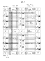
図1は、本発明の一実施の形態による半導体記憶装置において、そのチップ構成の一例を示す平面図であり、(a)は、チップ全体の構成例、(b)は、(a)におけるメモリブロックの構成例を示すものである。 FIG. 1 is a plan view showing an example of a chip configuration of a semiconductor memory device according to an embodiment of the present invention, where (a) is a configuration example of the entire chip, and (b) is a memory in (a). The structural example of a block is shown.
図1に示す半導体記憶装置は、プレート駆動方式のDRAMとなっている。そのメモリチップCHIP全体の構成は、例えば図1(a)に示すように、制御回路CNTLと、入出力回路DQCと、メモリブロックBLKとに大きく分けられる。制御回路CNTLには、クロック、アドレス、制御信号がメモリチップCHIP外から入力され、メモリチップCHIPの動作モードの決定やアドレスのプリデコード等が行われる。入出力回路DQCは、入出力バッファ等を備え、メモリチップCHIP外部からライトデータが入力され、メモリチップCHIP外部へリードデータを出力する。 The semiconductor memory device shown in FIG. 1 is a plate drive type DRAM. The entire configuration of the memory chip CHIP is roughly divided into a control circuit CNTL, an input / output circuit DQC, and a memory block BLK, for example, as shown in FIG. A clock, an address, and a control signal are input to the control circuit CNTL from outside the memory chip CHIP, and an operation mode of the memory chip CHIP is determined, an address is predecoded, and the like. The input / output circuit DQC includes an input / output buffer and the like, and receives write data from the outside of the memory chip CHIP and outputs read data to the outside of the memory chip CHIP.
メモリブロックBLKには、例えば図1(b)に示すように、複数のアレー状に配置されたメモリアレーARYが配置され、その周囲にはセンスアンプ列SAA、サブワードドライバ列SWDA、プレートドライバ列PLDA、クロスエリアXPが配置される。また、メモリブロックBLKの外周には、センスアンプ列SAAと平行に列デコーダYDECおよびメインアンプ列MAAが配置され、サブワードドライバ列SWDAと平行に行デコーダXDEC並びにアレー制御回路ACCが配置される。 For example, as shown in FIG. 1B, a plurality of memory arrays ARY arranged in an array are arranged in the memory block BLK. Around the memory blocks BLK, a sense amplifier array SAA, a sub word driver array SWDA, and a plate driver array PLDA are arranged. The cross area XP is arranged. On the outer periphery of the memory block BLK, a column decoder YDEC and a main amplifier row MAA are arranged in parallel with the sense amplifier row SAA, and a row decoder XDEC and an array control circuit ACC are arranged in parallel with the sub word driver row SWDA.
図2は、図1の半導体記憶装置において、そのメモリアレーとセンスアンプ列の構成の一例を示す回路図である。図2に示すように、メモリアレーARYは、複数のメモリセルMCから構成されている。メモリセルMCは、DRAMメモリセルとなっており、1個のMOSトランジスタ(メモリセルトランジスタ)および1個のキャパシタCsで構成され、MOSトランジスタの一方のソース又はドレインが、ビット線BLT又はビット線BLBに接続され、他方のソース又はドレインが、蓄積ノードSNに接続され、ゲートが、ワード線WLに接続されている。 FIG. 2 is a circuit diagram showing an example of the configuration of the memory array and the sense amplifier array in the semiconductor memory device of FIG. As shown in FIG. 2, the memory array ARY includes a plurality of memory cells MC. The memory cell MC is a DRAM memory cell, and is composed of one MOS transistor (memory cell transistor) and one capacitor Cs. One source or drain of the MOS transistor is the bit line BLT or the bit line BLB. The other source or drain is connected to the storage node SN, and the gate is connected to the word line WL.
キャパシタCsの一方の端子は、蓄積ノードSNに接続され、他方の端子は、ワード線WLと並行に配線されたプレート線PLに接続される。なお、ビット線BLTとビット線BLBは、ビット線対(相補ビット線)BLT/Bとして機能する。 One terminal of the capacitor Cs is connected to the storage node SN, and the other terminal is connected to a plate line PL wired in parallel with the word line WL. The bit line BLT and the bit line BLB function as a bit line pair (complementary bit line) BLT / B.
ここで、通常のDRAMと異なり、プレート線PLを1本のワード線WL毎に分割してワード線WLと並行に配線し、ワード線WLが活性化されたメモリセルMCのプレート線PLのみを駆動する構成にするとよい。これによって、プレート線PLの駆動に伴う他の非選択状態のメモリセルMCへのディスターブを低減しながら、蓄積ノードSNの電圧を増加できる効果が得られる。また、メモリアレーARYには、前述したメモリセルMCと同様の構成のダミーメモリセルDMCが含まれている。ダミーメモリセルDMCは、ダミーワード線DWLおよびダミープレート線DPLに接続され、読み出し時の参照信号発生に用いられる。 Here, unlike a normal DRAM, the plate line PL is divided into one word line WL and wired in parallel with the word line WL, and only the plate line PL of the memory cell MC in which the word line WL is activated is provided. It is preferable to use a driving structure. As a result, it is possible to increase the voltage of the storage node SN while reducing disturbance to the other non-selected memory cells MC accompanying the driving of the plate line PL. The memory array ARY includes dummy memory cells DMC having the same configuration as the memory cell MC described above. The dummy memory cell DMC is connected to the dummy word line DWL and the dummy plate line DPL, and is used for generating a reference signal at the time of reading.
図3は、図1の半導体記憶装置において、そのセンスアンプ列とサブワードドライバ列とプレートドライバ列の詳細な配置関係の一例を示す平面図である。図3に示すように、センスアンプ列SAA内のセンスアンプSAは、メモリアレーARYに対して上下に交互配置され、上下のメモリアレーARY内のビット線対BLT/Bに共通接続される。 FIG. 3 is a plan view showing an example of a detailed arrangement relationship among the sense amplifier row, the sub word driver row, and the plate driver row in the semiconductor memory device of FIG. As shown in FIG. 3, the sense amplifiers SA in the sense amplifier array SAA are alternately arranged above and below the memory array ARY and commonly connected to the bit line pairs BLT / B in the upper and lower memory arrays ARY.
同様に、サブワードドライバ列SWDA内のサブワードドライバSWDとプレートドライバ列PLDA内のプレートドライバPLDも、それぞれ、メモリアレーARYに対して左右に交互配置され、左右のメモリアレーARY内のワード線WLとプレート線PLに共通接続される。このように配置することにより、サブワードドライバ列SWDA内およびプレートドライバ列PLDA内において、サブワードドライバSWD間及びプレートドライバPLD間のピッチを、メモリアレーARY内のワード線WL間およびプレート線PL間のピッチの2倍に広げることができる。したがって、微細化が容易となる。 Similarly, the sub word driver SWD in the sub word driver column SWDA and the plate driver PLD in the plate driver column PLDA are alternately arranged on the left and right with respect to the memory array ARY, respectively, and the word lines WL and the plates in the left and right memory arrays ARY are arranged. Commonly connected to the line PL. With this arrangement, the pitch between the sub-word drivers SWD and the plate drivers PLD in the sub-word driver column SWDA and the plate driver column PLDA is set to the pitch between the word lines WL and the plate lines PL in the memory array ARY. Can be doubled. Therefore, miniaturization becomes easy.
図4は、図2の半導体記憶装置において、そのセンスアンプ列の詳細な構成の一例を示す回路図である。図4に示すように、センスアンプ列SAAには複数のセンスアンプSAが配置され、各センスアンプSAは、隣接する両側のメモリアレーARYのビット線対BLT/Bに共通接続されている。そして、各センスアンプSA内には、トランスファーゲートTGCと、プリチャージ回路PCCと、クロスカップル・アンプCCと、読み出し・書き込みポートIOPとが含まれている。 FIG. 4 is a circuit diagram showing an example of a detailed configuration of the sense amplifier array in the semiconductor memory device of FIG. As shown in FIG. 4, a plurality of sense amplifiers SA are arranged in the sense amplifier array SAA, and each sense amplifier SA is commonly connected to the bit line pairs BLT / B of the adjacent memory arrays ARY. Each sense amplifier SA includes a transfer gate TGC, a precharge circuit PCC, a cross couple amplifier CC, and a read / write port IOP.
トランスファーゲートTGCは、センスアンプ分離信号(SHR信号)が活性化された時にセンスアンプSAとメモリアレーARY間を接続する回路である。プリチャージ回路PCCは、ビット線プリチャージ信号(BLEQ信号)が活性化された時に対となるビット線BLT,BLB間をイコライズし、ビット線プリチャージレベルVBLRにプリチャージする。ビット線プリチャージレベルVBLRは、通常、ビット線振幅の電圧VDL(チップ外部からの電源電圧VCCと同レベルかまたはそれを降圧したレベル)の中点VDL/2に設定される。 The transfer gate TGC is a circuit that connects between the sense amplifier SA and the memory array ARY when the sense amplifier isolation signal (SHR signal) is activated. The precharge circuit PCC equalizes the paired bit lines BLT and BLB when the bit line precharge signal (BLEQ signal) is activated, and precharges the bit line precharge level VBLR. The bit line precharge level VBLR is normally set to the midpoint VDL / 2 of the voltage VDL of the bit line amplitude (the same level as the power supply voltage VCC from the outside of the chip or a level obtained by reducing it).
クロスカップル・アンプCCは、ビット線BLT,BLB上にメモリセルMCおよびダミーメモリセルDMCからの微小な読出し信号が発生した後に、P側共通ソース線CSPを電圧VDLに駆動し、N側共通ソース線CSNを接地電圧VSSに駆動して、ビット線BLTとビット線BLBのうちの電圧の高い方を電圧VDLに、低い方を接地電圧VSSに増幅し、増幅された電圧をラッチする回路である。読み出し・書き込みポートIOPは、列選択線YSが活性化されたときにローカルIO線(LIO線)LIOT/Bとビット線対BLT/Bを接続する回路である。なお、LIO線LIOT/Bは、非選択センスアンプ列SAAでの電流消費を防止するために、待機時にはプリチャージレベルに保持される。 The cross-couple amplifier CC drives the P-side common source line CSP to the voltage VDL after a minute read signal from the memory cell MC and the dummy memory cell DMC is generated on the bit lines BLT and BLB, and the N-side common source This circuit drives the line CSN to the ground voltage VSS, amplifies the higher one of the bit line BLT and the bit line BLB to the voltage VDL, the lower one to the ground voltage VSS, and latches the amplified voltage. . The read / write port IOP is a circuit that connects the local IO line (LIO line) LIOT / B and the bit line pair BLT / B when the column selection line YS is activated. Note that the LIO line LIOT / B is held at the precharge level during standby in order to prevent current consumption in the non-selected sense amplifier array SAA.
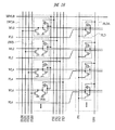
図5は、図1の半導体記憶装置において、そのクロスエリアの構成の一例を示す回路図である。クロスエリアXPは、SHR信号ドライバSHDと、LIO線プリチャージ回路REQと、リードライトゲートRGCと、CS線ドライバCSDと、CS線プリチャージ回路SEQと、BLEQ信号ドライバEQDと、FX線ドライバFXDと、PX線ドライバPXDとを含んでいる。 FIG. 5 is a circuit diagram showing an example of the configuration of the cross area in the semiconductor memory device of FIG. The cross area XP includes an SHR signal driver SHD, an LIO line precharge circuit REQ, a read / write gate RGC, a CS line driver CSD, a CS line precharge circuit SEQ, a BLEQ signal driver EQD, and an FX line driver FXD. PX line driver PXD.
SHR信号ドライバSHDは、SHR信号の相補信号SHRBが入力され、その反転信号を出力する。LIO線プリチャージ回路REQは、リードライトイネーブル信号RWEが非活性状態のVSSレベルのときに、LIO線LIOT/Bを電圧VPCにプリチャージする。リードライトゲートRGCは、リードライトイネーブル信号RWEが活性状態の電圧VCL(外部VCCレベルと同じかまたはそれを降圧したレベルで周辺回路用電源電圧として用いられる)のときにLIO線LIOT/BとメインIO線MIOT/Bとを接続する回路である。 The SHR signal driver SHD receives a complementary signal SHRB of the SHR signal and outputs an inverted signal thereof. The LIO line precharge circuit REQ precharges the LIO line LIOT / B to the voltage VPC when the read / write enable signal RWE is at the inactive VSS level. The read / write gate RGC is connected to the LIO line LIOT / B and the main when the read / write enable signal RWE is at the active state voltage VCL (the same as or lower than the external VCC level is used as the peripheral circuit power supply voltage). This is a circuit for connecting the IO line MIOT / B.
CS線ドライバCSDは、N側センスアンプイネーブル信号SANが活性状態のときに、N側共通ソース線CSNを接地電圧VSSに駆動し、第1のP側センスアンプイネーブル信号SAP1Bが活性状態(VSSレベル)のときに、P側共通ソース線CSPを電圧VDL(ビット線の‘H’レベル)に駆動し、第2のP側センスアンプイネーブル信号SAP2が活性状態(VCLレベル)のときに、P側共通ソース線CSPを電圧VSPに駆動する回路である。 The CS line driver CSD drives the N-side common source line CSN to the ground voltage VSS when the N-side sense amplifier enable signal SAN is in the active state, and the first P-side sense amplifier enable signal SAP1B is in the active state (the VSS level). ), When the P-side common source line CSP is driven to the voltage VDL ('H' level of the bit line) and the second P-side sense amplifier enable signal SAP2 is in the active state (VCL level), This is a circuit for driving the common source line CSP to the voltage VSP.
なお、ここでは、P側共通ソース線CSPを電圧VDLに駆動する回路としてPチャネルMOSトランジスタを、電圧VSPに駆動する回路としてNチャネルMOSトランジスタを用いている。電圧VSPに駆動する回路は、後述するが、書き込み時の‘H’側のビット線電圧を一時下げるためのものなのでNチャネルMOSトランジスタとしている。これによって、高速にビット線電圧を下げることが可能になる。ただし、これをPチャネルMOSトランジスタで構成することも可能である。 Here, a P-channel MOS transistor is used as a circuit for driving the P-side common source line CSP to the voltage VDL, and an N-channel MOS transistor is used as a circuit for driving to the voltage VSP. As will be described later, the circuit driven to the voltage VSP is an N-channel MOS transistor because it temporarily lowers the bit line voltage on the ‘H’ side during writing. As a result, the bit line voltage can be lowered at high speed. However, this can also be constituted by a P-channel MOS transistor.
このように、本発明においては、CS線ドライバCSD内に、センスアンプSAが活性化状態におけるP側共通ソース線CSPのレベルを、電圧VDLと電圧VSPの2種類に設定可能な機能を備えたことを特徴としている。この際に、CS線ドライバCSDをクロスエリアXPに配置すると、センスアンプSAの面積が増加しないという利点がある。 As described above, in the present invention, the CS line driver CSD has a function capable of setting the level of the P-side common source line CSP when the sense amplifier SA is activated to two kinds of voltage VDL and voltage VSP. It is characterized by that. At this time, if the CS line driver CSD is arranged in the cross area XP, there is an advantage that the area of the sense amplifier SA does not increase.
CS線プリチャージ回路SEQは、BLEQ信号が活性化されたときにP側,N側共通ソース線CSP,CSNをVDL/2にプリチャージする回路である。BLEQ信号ドライバEQDは、プリチャージ信号BLEQの相補信号BLEQBが入力され、その反転信号を出力する。FX線ドライバFXDは、信号FXBが入力され、その相補信号をサブワードドライバ選択線FX(FX線)に出力する。 The CS line precharge circuit SEQ is a circuit that precharges the P-side and N-side common source lines CSP and CSN to VDL / 2 when the BLEQ signal is activated. The BLEQ signal driver EQD receives a complementary signal BLEQB of the precharge signal BLEQ and outputs an inverted signal thereof. The FX line driver FXD receives the signal FXB and outputs a complementary signal to the sub word driver selection line FX (FX line).
PX線ドライバPXDは、電圧VCL振幅のプレートタイミング信号PXSが入力され、プレート制御線(PX線)に電圧を出力する。PX線は、プレート線PLを駆動するための配線である。プレートタイミング信号PXSが非活性の場合、PX線には、通常時のプレート電圧VPHが出力される。一方、プレートタイミング信号PXSが活性化された場合、PX線には、プレート電圧VPLが出力される。なお、PX線ドライバPXDをクロスエリアXPに配置することにより、PX線の遅延を低減することが可能である。 The PX line driver PXD receives the plate timing signal PXS having the voltage VCL amplitude and outputs a voltage to the plate control line (PX line). The PX line is a wiring for driving the plate line PL. When the plate timing signal PXS is inactive, the normal plate voltage VPH is output to the PX line. On the other hand, when the plate timing signal PXS is activated, the plate voltage VPL is output to the PX line. Note that by arranging the PX line driver PXD in the cross area XP, it is possible to reduce the delay of the PX line.
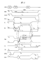
つぎに、これまでに説明したような半導体記憶装置の動作について説明する。図6は、図1の半導体記憶装置において、その動作の一例を示す動作波形図である。 Next, the operation of the semiconductor memory device as described above will be described. FIG. 6 is an operation waveform diagram showing an example of the operation of the semiconductor memory device of FIG.
図6に示すように、メモリチップ外部からバンク活性化コマンドACTが入力されると、まず、アドレスで指定されたセンスアンプ列SAAにおいてSHR信号の片側とBLEQ信号が非活性化される。また、活性化状態でVPPレベルであったダミーセルDMCのダミーワード線DWL1が非活性化され、VKKレベルに復帰する。ここでVKKは、負電源発生回路により発生されたワード線の低レベル側の電源電圧である。このように、非活性化時のワード線レベルを接地電圧VSSよりも低くすることにより、メモリセルトランジスタのしきい値電圧を低く設定することができ、ワード線の‘H’側のレベルVPPを低減することができる。 As shown in FIG. 6, when a bank activation command ACT is input from the outside of the memory chip, first, one side of the SHR signal and the BLEQ signal are deactivated in the sense amplifier array SAA specified by the address. Further, the dummy word line DWL1 of the dummy cell DMC that has been at the VPP level in the activated state is deactivated and returns to the VKK level. Here, VKK is a power supply voltage on the low level side of the word line generated by the negative power supply generation circuit. As described above, the threshold voltage of the memory cell transistor can be set low by setting the word line level at the time of deactivation below the ground voltage VSS, and the level VPP on the 'H' side of the word line is set to be lower. Can be reduced.
その後、行デコーダXDECにおいてメインワード線MWLBが電圧VKKに下がり、アレー制御回路ACCにおいてFX線が活性化されると、選択されたワード線WL0が電圧VPPに活性化される。ワード線WL0によって選択されたメモリセルMCにおいては、メモリセルトランジスタが導通し、ビット線BLT上に信号が読み出される。図6では、メモリセルMCに予め接地電圧VSSが書き込まれており、‘L’の信号が発生した例を示している。また、ワード線WL0の活性化と同時にダミーワード線DWL1も活性化され、プリチャージ電圧VBLRが書き込まれていたダミーメモリセルDMCからビット線BLB上に参照信号が発生する。 Thereafter, when the main word line MWLB falls to the voltage VKK in the row decoder XDEC and the FX line is activated in the array control circuit ACC, the selected word line WL0 is activated to the voltage VPP. In the memory cell MC selected by the word line WL0, the memory cell transistor becomes conductive, and a signal is read onto the bit line BLT. FIG. 6 shows an example in which the ground voltage VSS is written in the memory cell MC in advance, and a signal of 'L' is generated. The dummy word line DWL1 is activated simultaneously with the activation of the word line WL0, and a reference signal is generated on the bit line BLB from the dummy memory cell DMC in which the precharge voltage VBLR has been written.
なお、この際に、選択されたメモリセルMCのプレート線PL0と、それに対応するダミーメモリセルDMCのプレート線DPL1が電圧VPHから電圧VPLへと立ち下げられる。このように、プレート線PL0を駆動すると、選択されたメモリセルMCの蓄積ノードSNとダミーメモリセルDMCのダミー蓄積ノードDSNは、キャパシタCsを介したカップリングによって電圧レベルが下がるため、それぞれの蓄積電荷が高速にビット線BLT,BLB上に読み出される。ここで、電圧VPHは、電圧VDLと接地電圧VSSのほぼ中間の電圧にしておくと、待機時にメモリセルの容量絶縁膜に印加される電圧が小さくなるので、信頼性が高くなる。 At this time, the plate line PL0 of the selected memory cell MC and the corresponding plate line DPL1 of the dummy memory cell DMC are lowered from the voltage VPH to the voltage VPL. As described above, when the plate line PL0 is driven, the voltage level of the storage node SN of the selected memory cell MC and the dummy storage node DSN of the dummy memory cell DMC is lowered by the coupling through the capacitor Cs. Charge is read onto the bit lines BLT and BLB at high speed. Here, if the voltage VPH is set to a voltage approximately halfway between the voltage VDL and the ground voltage VSS, the voltage applied to the capacitor insulating film of the memory cell during standby is reduced, and thus the reliability is increased.
その後、センスアンプSAにおいて、P側共通ソース線CSPを電圧VDLに、N側共通ソース線CSNを接地電圧VSSに駆動し、ビット線BLT,BLB上の電圧差を増幅する。この状態で、メモリチップはリードコマンドRDまたはライトコマンドWRTを受け付けることができる。図6ではライトコマンドWRTが入力された場合を示している。そして、選択されたアドレスの列選択線YSが活性化され、LIO線LIOT/Bから、ライトデータが書き込まれる。ここでは、ビット線BLTが‘H’に駆動される反転書込み時の波形を示している。 Thereafter, in the sense amplifier SA, the P-side common source line CSP is driven to the voltage VDL and the N-side common source line CSN is driven to the ground voltage VSS, and the voltage difference on the bit lines BLT and BLB is amplified. In this state, the memory chip can accept a read command RD or a write command WRT. FIG. 6 shows a case where the write command WRT is input. Then, the column selection line YS of the selected address is activated, and write data is written from the LIO line LIOT / B. Here, a waveform at the time of inversion writing in which the bit line BLT is driven to “H” is shown.
メモリセルトランジスタは、NチャネルMOSトランジスタなので、しきい値電圧をVTとすると、蓄積ノードSNへ書きこむことができる最大の電圧はVPP−VTとなる。本発明のメモリチップでは、メモリセルトランジスタのゲート酸化膜を薄膜化するために、ワード線の‘H’レベル電圧VPPを、電源電圧VDD(たとえば1.8V)程度まで下げている。また、メモリセルトランジスタは微細なトランジスタを用いており、個数も多いため、しきい値電圧VTのばらつきが1V近くと非常に大きく、例えば設計中心値を0.7Vとした場合、最小値は0.2V、最大値は1.2Vになる。 Since the memory cell transistor is an N-channel MOS transistor, when the threshold voltage is VT, the maximum voltage that can be written to storage node SN is VPP-VT. In the memory chip of the present invention, the ‘H’ level voltage VPP of the word line is lowered to about the power supply voltage VDD (for example, 1.8V) in order to reduce the gate oxide film of the memory cell transistor. Further, since the memory cell transistor uses a fine transistor and has a large number, the variation of the threshold voltage VT is very large as close to 1V. For example, when the design center value is 0.7V, the minimum value is 0. .2V, the maximum value is 1.2V.
そうすると、ビット線電圧VDLを一例として1.3Vとした場合、しきい値電圧VTが低いメモリセル(LVT−cell)ではVPP−VT=1.6Vなのでメモリセルトランジスタがオンしており、蓄積ノードSNにVDL=1.3Vを書き込むことができる。一方、しきい値電圧VTが中程度のメモリセル(MVT−cell)、しきい値電圧VTが高いメモリセル(HVT−cell)では、増幅の途中でカットオフ状態となり、それぞれ1.1V、0.6Vまでしか書き込まれない。すなわち、書込み時の蓄積ノードSNの電圧は、メモリセルトランジスタのしきい値電圧VTに対応して0.6Vから1.3Vまでのばらつきを持つ。 Then, when the bit line voltage VDL is set to 1.3 V as an example, in the memory cell (LVT-cell) having a low threshold voltage VT, VPP-VT = 1.6 V, so the memory cell transistor is turned on, and the storage node VDL = 1.3V can be written to SN. On the other hand, in a memory cell (MVT-cell) having a medium threshold voltage VT and a memory cell (HVT-cell) having a high threshold voltage VT, a cut-off state occurs in the middle of amplification, and 1.1V and 0 respectively. Only written up to 6V. That is, the voltage of storage node SN at the time of writing varies from 0.6 V to 1.3 V corresponding to the threshold voltage VT of the memory cell transistor.
この状態で、プリチャージコマンドPRCが入力されたときに、選択されたメモリセルMCのプレート線PL0とダミーメモリセルDMCのダミープレート線DPL1を電圧VPLから電圧VPHに復帰させると、それぞれの蓄積ノードSN,DSNの電圧は、キャパシタCsからのカップリングを受け、ΔPL=VPH−VPL分だけ上昇する。この際に、‘H’が書き込まれたメモリセルMCでは、メモリセルトランジスタがカットオフするかコンダクタンスが高い状態であるために、ΔPLの電圧上昇分が保持されるが、‘L’が書き込まれたメモリセルMCではメモリセルトランジスタが十分にオン状態であるために、すぐに接地電圧VSSに復帰する。したがって、メモリセルMCの蓄積ノードSNの蓄積電荷量をΔPLだけ増加することができる。 In this state, when the precharge command PRC is input, if the plate line PL0 of the selected memory cell MC and the dummy plate line DPL1 of the dummy memory cell DMC are returned from the voltage VPL to the voltage VPH, the respective storage nodes The voltages of SN and DSN are increased by ΔPL = VPH−VPL due to coupling from the capacitor Cs. At this time, in the memory cell MC in which “H” is written, since the memory cell transistor is cut off or the conductance is high, the voltage increase of ΔPL is held, but “L” is written. In the memory cell MC, since the memory cell transistor is sufficiently on, it immediately returns to the ground voltage VSS. Therefore, the amount of charge stored in storage node SN of memory cell MC can be increased by ΔPL.
ここで、ΔPLを、最もしきい値電圧VTの高いメモリセル(HVT−cell)の書込み電圧がVDLまで上昇するように例えば0.7Vに設定すると、全てのメモリセルMCが1.3V以上に書き込まれるため、次のサイクルでの読み出し信号量やリテンション時間のマージンを広げることができる。しかしながら、しきい値電圧VTの低いメモリセル(LVT−cell)では、もともとVDL=1.3Vまで書き込まれていたので、さらに電圧がΔPL分だけ上昇すると2.0Vにまで高くなる。このままワード線を非活性化すると、待機時にメモリセルトランジスタに高い電圧が印加されたままとなり、デバイスの信頼性が低下する。 Here, if ΔPL is set to, for example, 0.7 V so that the write voltage of the memory cell (HVT-cell) having the highest threshold voltage VT rises to VDL, all the memory cells MC become 1.3 V or higher. Since data is written, it is possible to widen the read signal amount and the retention time margin in the next cycle. However, since the memory cell (LVT-cell) having a low threshold voltage VT was originally written up to VDL = 1.3 V, when the voltage further increases by ΔPL, the voltage increases to 2.0 V. If the word line is deactivated as it is, a high voltage remains applied to the memory cell transistor during standby, and the reliability of the device decreases.
そこで、本発明では次のような方法でしきい値電圧VTの低いメモリセルMCだけを選択的に放電し、ワード線非活性時の蓄積ノードSNへの書込み電圧を揃えることで、デバイスの信頼性を高める。すなわち、例えばプリチャージコマンドPRCの入力に次いでプレート線PLを駆動した後のタイミングで、図5で述べたCS線ドライバCSDによってP側共通ソース線CSPを電圧VSPまで下げることにより、‘H’側のビット線電圧をVDP(例えば0.7V)まで下げる。 Therefore, in the present invention, only the memory cells MC having a low threshold voltage VT are selectively discharged by the following method, and the write voltage to the storage node SN when the word line is inactive is made uniform. Increase sex. That is, for example, at the timing after the plate line PL is driven after the input of the precharge command PRC, the P-side common source line CSP is lowered to the voltage VSP by the CS line driver CSD described in FIG. Is lowered to VDP (for example, 0.7 V).
そうすると、しきい値電圧VTの低いメモリセルMCにおけるメモリセルトランジスタでは、実効ゲート電圧VGS−VTが(1.8−0.7)−0.2=0.9Vとなり、強くオンするため、蓄積ノードSNの電荷が急速に放電される。一方、しきい値電圧VTが中程度のメモリセルでは、VGS−VTが0.4Vとなり、弱くオンするため放電は緩やかであり、しきい値電圧VTが高いメモリセルでは、VGS−VTが負であるためカットオフの状態が保たれる。 Then, in the memory cell transistor in the memory cell MC having a low threshold voltage VT, the effective gate voltage VGS−VT is (1.8−0.7) −0.2 = 0.9V, which is strongly turned on. The charge on the node SN is rapidly discharged. On the other hand, VGS−VT is 0.4 V in a memory cell with a medium threshold voltage VT, and the discharge is slow because it is weakly turned on. VGS−VT is negative in a memory cell with a high threshold voltage VT. Therefore, the cut-off state is maintained.
したがって、図6に示すように、しきい値電圧VTの低いメモリセル(LVT−cell)では、過剰に書き込まれた電荷の放電によって上がりすぎた電圧が下がり、しきい値電圧の中程度のメモリセル(MVT−cell)および高いメモリセル(HVT−cell)では、電圧がほぼ保たれるため、しきい値電圧VTのばらつきよりも書込み電圧のばらつきが小さくなる。そして、このような放電動作の終了後は、ワード線WL0をたち下げ、BLEQ信号およびSHR信号を再び活性化させて、ビット線対BLT/Bをプリチャージする。 Therefore, as shown in FIG. 6, in the memory cell (LVT-cell) having a low threshold voltage VT, the voltage that has risen excessively due to the discharge of the excessively written charge decreases, and the memory with a medium threshold voltage is obtained. In the cell (MVT-cell) and the high memory cell (HVT-cell), since the voltage is substantially maintained, the variation in the write voltage becomes smaller than the variation in the threshold voltage VT. After completion of such a discharge operation, the word line WL0 is lowered, the BLEQ signal and the SHR signal are activated again, and the bit line pair BLT / B is precharged.
以上のように、本発明の構成および動作を用いると、プレート駆動によってメモリセルに書き込まれる電荷量を増加し、リテンション特性や動作速度を改善すると共に、過剰な書き込み電荷の放電を行う調整手法によって、しきい値電圧のばらつきが大きい場合でも書き込み電荷量のばらつきを低減することができる。これによって、メモリセルトランジスタに高電圧が長時間印加されることを防ぐことが可能になるため、デバイスの信頼性が向上する。また、ワード線電圧を低減することができるため、メモリセルトランジスタのゲート酸化膜を薄膜化でき、微細化が可能となる。そして、DRAMチップの大容量化または、チップサイズの低減による製造コストの低減を実現することができる。 As described above, when the configuration and operation of the present invention are used, the amount of charge written to the memory cell by plate driving is increased, the retention characteristic and the operation speed are improved, and an adjustment method for discharging excessive write charge is used. Even when the variation in the threshold voltage is large, the variation in the write charge amount can be reduced. As a result, it is possible to prevent a high voltage from being applied to the memory cell transistor for a long time, so that the reliability of the device is improved. In addition, since the word line voltage can be reduced, the gate oxide film of the memory cell transistor can be thinned and miniaturized. In addition, it is possible to reduce the manufacturing cost by increasing the capacity of the DRAM chip or reducing the chip size.
ところで、これまでの説明においては、CS線ドライバCSD内に、センスアンプSAが活性化状態におけるP側共通ソース線CSPのレベルを、電圧VDLと電圧VSPの2種類に設定する例を示したが、加えて図7のように、オーバードライブセンス方式を組み合わせることも可能である。図7は、図5のクロスエリアにおいて、その構成を変形した一例を示す回路図である。 By the way, in the description so far, the example in which the level of the P-side common source line CSP when the sense amplifier SA is in the activated state is set to two types of the voltage VDL and the voltage VSP in the CS line driver CSD has been shown. In addition, it is possible to combine the overdrive sensing method as shown in FIG. FIG. 7 is a circuit diagram showing an example of a modified configuration in the cross area of FIG.
図7に示すクロスエリアXPは、前述したプレート駆動方式とオーバードライブセンス方式を組み合わせて用いる際の回路構成例となっており、図5に示した回路と比較して、CS線ドライバCSDの構成が異なっている。すなわち、図7に示すCS線ドライバCSDでは、初期のP側センスアンプイネーブル信号SAP0Bが活性状態のときに、P側共通ソース線CSPを一時的にオーバードライブ電圧VODへ駆動するためのPMOSトランジスタが追加されている。電圧VODは、最終的なビット線の‘H’レベル電圧VDLよりも高い電圧であり、センスアンプSAの増幅動作を高速化するためのものである。なお、このようにしてドライバの種類を増やしても、CS線ドライバCSDをクロスエリアXPに配置しているため、センスアンプの面積が増加せず、微細化が可能になるという利点がある。 The cross area XP shown in FIG. 7 is an example of a circuit configuration when the plate driving method and the overdrive sensing method described above are used in combination, and the configuration of the CS line driver CSD is compared with the circuit shown in FIG. Are different. That is, in the CS line driver CSD shown in FIG. 7, when the initial P-side sense amplifier enable signal SAP0B is active, the PMOS transistor for temporarily driving the P-side common source line CSP to the overdrive voltage VOD is provided. Have been added. The voltage VOD is higher than the final “H” level voltage VDL of the bit line, and is for speeding up the amplification operation of the sense amplifier SA. Even if the number of types of drivers is increased in this way, the CS line driver CSD is arranged in the cross area XP, so there is an advantage that the area of the sense amplifier does not increase and miniaturization is possible.
図8は、図7のクロスエリアにおいて、CS線ドライバで使用する電圧の発生方式の一例を示す概略図である。オーバードライブ電圧VODは、最終的なビット線の‘H’レベル電圧VDLよりも高い電圧であるため、例えば図8に示すように、メモリチップCHIP外部から供給される外部電源電圧VDDをそのまま用いることができる。ビット線の‘H’レベル電圧VDLは、外部電源電圧VDDを降圧回路DC1で降圧して発生する。電圧VSPは、その値として、図6で述べた放電動作時のビット線電圧VDPよりも、クロスカップル・アンプCCにおけるPMOSトランジスタのしきい値電圧分だけ低くする必要がある。このため、降圧回路DC2を用いてビット線電圧の半分VDL/2よりも低い値へ降圧するか、または接地電圧VSSをそのまま用いることが望ましい。 FIG. 8 is a schematic diagram showing an example of a voltage generation method used in the CS line driver in the cross area of FIG. Since the overdrive voltage VOD is higher than the final “H” level voltage VDL of the bit line, for example, as shown in FIG. 8, the external power supply voltage VDD supplied from the outside of the memory chip CHIP is used as it is. Can do. The 'H' level voltage VDL of the bit line is generated by stepping down the external power supply voltage VDD by the step-down circuit DC1. The voltage VSP needs to be lower than the bit line voltage VDP during the discharge operation described in FIG. 6 by the threshold voltage of the PMOS transistor in the cross-coupled amplifier CC. Therefore, it is desirable to use the step-down circuit DC2 to step down to a value lower than half the bit line voltage VDL / 2, or to use the ground voltage VSS as it is.
このように、プレート駆動方式とオーバードライブセンス方式を組み合わせた場合は、例えば図9に示すような動作となる。図9は、図1の半導体記憶装置において、図7のクロスエリアを用いた場合の動作の一例を示す波形図である。図9に示す動作波形は、前述した図6の動作波形と異なり、センスアンプSAによる増幅の初期にP側共通ソース線CSPを一時的にオーバードライブ電圧VODで駆動している。そして、ビット線対BLT/Bが十分に増幅された後、P側共通ソース線CSPは電圧VDLに駆動される。このような駆動を行うと、読み出し動作時および再書き込み動作時にビット線の増幅動作が高速化される。これ以降の動作は図6と同様である。 Thus, when the plate driving method and the overdrive sensing method are combined, the operation is as shown in FIG. 9, for example. FIG. 9 is a waveform diagram showing an example of the operation when the cross area of FIG. 7 is used in the semiconductor memory device of FIG. The operation waveform shown in FIG. 9 is different from the operation waveform of FIG. 6 described above, and the P-side common source line CSP is temporarily driven with the overdrive voltage VOD at the initial stage of amplification by the sense amplifier SA. After the bit line pair BLT / B is sufficiently amplified, the P-side common source line CSP is driven to the voltage VDL. When such driving is performed, the speed of the bit line amplification operation is increased during the read operation and the rewrite operation. The subsequent operation is the same as in FIG.
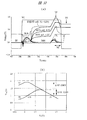
図10は、図6における動作を回路シミュレーションで再現したものであり、(a)は、その動作における主要部の波形図、(b)は、その動作におけるしきい値電圧と書き込み電圧の関係を示すグラフである。図10(a)では、図6で説明したように、ワード線WLを1.8Vに活性化し、プレート線PLを0.7V下げた状態で、ビット線BLT,BLB上に信号が発生している。ここで、ビット線BLT,BLBの信号増幅を開始し、次いで反転書き込みを行うと、しきい値電圧VTの違いによって蓄積ノードSNへの書き込み電圧のばらつきが発生する。 FIG. 10 is a reproduction of the operation in FIG. 6 by circuit simulation. (A) is a waveform diagram of the main part in the operation, and (b) is the relationship between the threshold voltage and the write voltage in the operation. It is a graph to show. In FIG. 10A, as described in FIG. 6, a signal is generated on the bit lines BLT and BLB with the word line WL activated to 1.8V and the plate line PL lowered by 0.7V. Yes. Here, when signal amplification of the bit lines BLT and BLB is started and then inversion writing is performed, a variation in the writing voltage to the storage node SN occurs due to a difference in threshold voltage VT.
その後、プレート線PLの電圧を上昇させると、‘H’が書き込まれたメモリセルMCにおける蓄積ノードSNの電圧は上昇するが、‘L’側のダミーメモリセルDMCにおけるダミー蓄積ノードDSNの電圧は、一旦上昇後、即座に接地電圧VSSに復帰する。‘H’が書き込まれたメモリセルMCにおいては、DCで示した期間、ビット線BLTの電圧を下げることで、過剰に書き込まれた電荷を放電させる。これによって、最終的な書き込み電圧のばらつきが低減されている。 Thereafter, when the voltage of the plate line PL is increased, the voltage of the storage node SN in the memory cell MC in which “H” is written increases, but the voltage of the dummy storage node DSN in the dummy memory cell DMC on the “L” side is Once it rises, it immediately returns to the ground voltage VSS. In the memory cell MC in which 'H' is written, the voltage written in excess is discharged by lowering the voltage of the bit line BLT during the period indicated by DC. As a result, variations in the final write voltage are reduced.
図10(b)に示すグラフは、横軸にメモリセルトランジスタのしきい値電圧VTを示し、縦軸に、蓄積ノードSNにおける、プレート駆動直後の期間での電圧VPと放電動作を7ns行いワード線を非活性化した直後の期間での電圧VSを示している。しきい値電圧VTのばらつき範囲を0.2〜1.2Vと仮定すると、図10(b)に示すように、プレート駆動直後の期間での蓄積ノードSNの最大電圧VPは2.0V近くになり、ばらつきΔVPは0.80Vになる。すなわち、放電動作なしでは、0.80V分の過剰電圧がメモリセルトランジスタに印加される。 In the graph shown in FIG. 10B, the horizontal axis indicates the threshold voltage VT of the memory cell transistor, and the vertical axis indicates the word VP and the discharge operation in the period immediately after the plate driving in the storage node SN for 7 ns. The voltage VS in the period immediately after the line is deactivated is shown. Assuming that the variation range of the threshold voltage VT is 0.2 to 1.2 V, as shown in FIG. 10B, the maximum voltage VP of the storage node SN in the period immediately after the plate driving is close to 2.0 V. Thus, the variation ΔVP becomes 0.80V. That is, without a discharge operation, an excess voltage of 0.80 V is applied to the memory cell transistor.
一方、放電動作を行った場合、最終的な蓄積ノードSNの電圧は、電圧VSまで放電されるため、VT=0.7V付近で最大値1.3Vをとるが、ばらつきはΔVS=0.34Vとなり、メモリセルトランジスタに印加される過剰電圧が43%まで抑制されている。これによって、メモリセルトランジスタの信頼性が向上し、微細化が容易となる。 On the other hand, when the discharge operation is performed, the final voltage of the storage node SN is discharged to the voltage VS, and thus takes a maximum value of 1.3 V in the vicinity of VT = 0.7 V, but the variation is ΔVS = 0.34 V. Thus, the excessive voltage applied to the memory cell transistor is suppressed to 43%. This improves the reliability of the memory cell transistor and facilitates miniaturization.
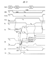
図11および図12は、図1の半導体記憶装置において、図6を変形した動作の一例を示す動作波形図である。図11に示す動作は、図6に示した動作に対して、プレート線PLを電圧VPLから電圧VPHへ上昇させる動作と、P側共通ソース線CSPの電圧VSPへの駆動とを同時に行った場合を示している。図6においては、プレート線PLの電圧を上昇させた直後に短時間ながら、蓄積ノードSNの電圧が上昇し、メモリセルトランジスタに高電圧が印加される。 11 and 12 are operation waveform diagrams showing an example of a modified operation of FIG. 6 in the semiconductor memory device of FIG. The operation shown in FIG. 11 is a case where the operation of raising the plate line PL from the voltage VPL to the voltage VPH and the driving of the P-side common source line CSP to the voltage VSP are performed simultaneously with respect to the operation shown in FIG. Is shown. In FIG. 6, the voltage at the storage node SN rises for a short time immediately after raising the voltage of the plate line PL, and a high voltage is applied to the memory cell transistor.
一方、図11に示す動作では、プレート線PLの駆動による蓄積ノードSNの電圧上昇と、しきい値電圧VTが低いメモリセルからの過剰電荷の放電が同時に起こるために、蓄積ノードSNにピーク電圧が発生しない。したがって、メモリセルトランジスタへの高電圧の印加を抑制することが可能となり、デバイスの信頼性をさらに向上させることができ、微細化が容易となる。 On the other hand, in the operation shown in FIG. 11, since the voltage rise of the storage node SN due to the driving of the plate line PL and the discharge of excess charges from the memory cell having a low threshold voltage VT occur simultaneously, the peak voltage is applied to the storage node SN. Does not occur. Therefore, application of a high voltage to the memory cell transistor can be suppressed, device reliability can be further improved, and miniaturization is facilitated.
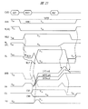
また、図12に示す動作は、図11の動作に対して、プレート線PLを電圧VPHから電圧VPLへ下降させるタイミングを、センスアンプ活性化後まで遅らせた場合を示している。この場合、ビット線対BLT/Bへの信号読み出し時にプレート線PLが一定電圧のままなので、ワード線活性化後の信号発生はやや遅くなるものの、センスアンプ増幅時の参照電圧としてビット線プリチャージ電圧VBLRをそのまま用いることができる。これによって、ダミーメモリセルDMCが不要となり、チップサイズを低減することが可能となる。また、図12に示す動作は、前述したプレート線PLのタイミング変更に加えて、センスアンプ活性化時にP側共通ソース線CSPを一時的にオーバードライブ電圧VODで駆動し、センス動作を高速化した場合を示している。 Further, the operation shown in FIG. 12 shows a case where the timing of lowering the plate line PL from the voltage VPH to the voltage VPL is delayed from the operation of FIG. 11 until after the sense amplifier is activated. In this case, since the plate line PL remains at a constant voltage when reading a signal to the bit line pair BLT / B, signal generation after activation of the word line is slightly delayed, but the bit line precharge is used as a reference voltage when the sense amplifier is amplified. The voltage VBLR can be used as it is. As a result, the dummy memory cell DMC becomes unnecessary, and the chip size can be reduced. In addition to the timing change of the plate line PL described above, the operation shown in FIG. 12 speeds up the sensing operation by temporarily driving the P-side common source line CSP with the overdrive voltage VOD when the sense amplifier is activated. Shows the case.
図13は、図1の半導体記憶装置において、そのメモリアレーのレイアウトの一例を示す図であり、(a)は、トランジスタの活性領域から蓄積ノードまでのレイアウト、(b)は、プレート電極からプレート線までのレイアウトを示すものである。図14は、図13のレイアウトにおいて、そのA−A’間の断面構成の一例を示す図である。図13に示すレイアウトは、複数のワード線WL0〜4と複数の隣接したビット線対BLT/Bを含み、このビット線対BLT/Bによって相補動作を行う構成となっている。なお、本レイアウトは、ビット線対BLT/Bが1本のワード線と交差しており、二交点メモリアレーと呼ばれている。 13 is a diagram showing an example of the layout of the memory array in the semiconductor memory device of FIG. 1. FIG. 13A shows a layout from the active region of the transistor to the storage node, and FIG. 13B shows a layout from the plate electrode to the plate. It shows the layout up to the line. FIG. 14 is a diagram showing an example of a cross-sectional configuration between A-A ′ in the layout of FIG. 13. The layout shown in FIG. 13 includes a plurality of word lines WL0 to WL4 and a plurality of adjacent bit line pairs BLT / B, and a complementary operation is performed by the bit line pairs BLT / B. In this layout, the bit line pair BLT / B intersects with one word line and is called a two-intersection memory array.
図13(a)に示すレイアウトでは、複数の活性領域ACTがビット線と平行に形成され、各活性領域ACT上には、2本のワード線が延伸している。各活性領域ACT内では、この2本のワード線のそれぞれをゲートとする2つメモリセルトランジスタが形成される。この2つのメモリセルトランジスタのソース/ドレインの一端は、共通のビット線コンタクトBCによってビット線に接続され、他端は、それぞれ異なる蓄積ノードコンタクトSCによって、それぞれ異なる蓄積ノードSNに接続される。なお、各蓄積ノードSNのビット線方向の横幅は、例えば隣接するワード線2本分に重なる程度の大きさとすることができる。 In the layout shown in FIG. 13A, a plurality of active regions ACT are formed in parallel with the bit lines, and two word lines extend on each active region ACT. In each active region ACT, two memory cell transistors are formed with each of the two word lines as a gate. One end of the source / drain of these two memory cell transistors is connected to the bit line by a common bit line contact BC, and the other end is connected to different storage nodes SN by different storage node contacts SC. Note that the horizontal width of each storage node SN in the bit line direction can be set to a size that overlaps, for example, two adjacent word lines.
図13(b)に示すレイアウトは、図13(a)の複数の蓄積ノードSNと1対1で対応する形で複数のプレート電極PLEが形成され、また、複数のワード線WL0〜4と1対1で対応する形で複数のプレート線PL0〜4が形成されている。すなわち、複数のプレート線PL0〜4と複数のプレート電極PLEのレイアウトは、図13(a)での複数のワード線WL0〜4と複数の蓄積ノードSNのレイアウトとほぼ同一形状のレイアウトとすることができる。この場合、各プレート電極PLEのビット線方向の横幅は、隣接するプレート線2本分に重なる程度の大きさとなるため、各プレート電極PLEは、この重なるいずれかプレート線にプレートコンタクトPCを介して接続することができる。
In the layout shown in FIG. 13 (b), a plurality of plate electrodes PLE are formed in a one-to-one correspondence with the plurality of storage nodes SN in FIG. 13 (a), and the plurality of word lines WL0-4 and 1 A plurality of plate lines PL <b> 0 to PL <b> 4 are formed in a form corresponding to
各DRAMメモリセルは、図14に示すように、半導体基板PW上に形成されたNチャネルMOSトランジスタ(メモリセルトランジスタ)と、ビット線BLの上部に設けられたスタックキャパシタとを有するものとなっている。図14においては、絶縁膜SiO2によって分離された半導体基板PW内の活性領域ACT上に、2本のワード線WLが配置され、この2本のワード線WLをメモリセルトランジスタのゲートとして、そのソース/ドレインとなるN型拡散層領域Nが半導体基板PW内に設けられている。 As shown in FIG. 14, each DRAM memory cell has an N channel MOS transistor (memory cell transistor) formed on a semiconductor substrate PW and a stack capacitor provided above the bit line BL. Yes. In FIG. 14, two word lines WL are arranged on the active region ACT in the semiconductor substrate PW separated by the insulating film SiO 2 , and the two word lines WL are used as the gates of the memory cell transistors. An N-type diffusion layer region N serving as a source / drain is provided in the semiconductor substrate PW.
この2本のワード線WL間のN型拡散層領域N上には、コンタクトCBが配置され、その上部にビット線コンタクトBCが配置される。ビット線コンタクトBC上には、ワード線の延伸方向と直交する方向に形成されたビット線BLが配置される。一方、この2本のワード線WLの外側のN型拡散層領域N上には、それぞれ、コンタクトCBが配置され、その上部に蓄積ノードコンタクトSCが配置される。蓄積ノードコンタクトSCの上部には、層間絶縁膜(図示せず)の孔の内壁に形成された凹型(シリンダ形状)の蓄積ノードSNが配置され、蓄積ノードSNの内側にはプレート電極PLEが埋め込まれており、これらが容量絶縁膜CIを挟んでキャパシタCsを構成する。 A contact CB is disposed on the N-type diffusion layer region N between the two word lines WL, and a bit line contact BC is disposed thereon. A bit line BL formed in a direction orthogonal to the extending direction of the word line is disposed on the bit line contact BC. On the other hand, a contact CB is disposed on each of the N-type diffusion layer regions N outside the two word lines WL, and a storage node contact SC is disposed thereon. A concave (cylinder-shaped) storage node SN formed on the inner wall of a hole in an interlayer insulating film (not shown) is disposed above the storage node contact SC, and a plate electrode PLE is embedded inside the storage node SN. These constitute the capacitor Cs with the capacitive insulating film CI interposed therebetween.
プレート電極PLEの上部には、プレートコンタクトPCが配置され、ワード線方向に配線されたプレート線PLと接続される。図14では、深い孔に形成された蓄積ノードSN電極の内側だけをキャパシタとして用いるタイプのスタックキャパシタを示している。本キャパシタを用いると、蓄積ノードSNの上部でプレート電極PLEが分離できるため、分離プロセスが容易になる利点がある。また、蓄積ノードSN電極の内側のみでなく、内側と外側の両方を使うタイプのキャパシタとすることもできる。但し、この場合は、容量を大きくすることができるが、蓄積ノードSN電極の下部でプレート電極PLEを分離しなければならないため、分離プロセスが複雑になる問題がある。 A plate contact PC is disposed on the plate electrode PLE and is connected to the plate line PL wired in the word line direction. FIG. 14 shows a stack capacitor that uses only the inside of the storage node SN electrode formed in a deep hole as a capacitor. When this capacitor is used, the plate electrode PLE can be separated at the upper part of the storage node SN, so that there is an advantage that the separation process becomes easy. Further, not only the inside of the storage node SN electrode but also a capacitor using both the inside and the outside can be used. In this case, however, the capacity can be increased, but the plate electrode PLE must be separated under the storage node SN electrode, which causes a problem that the separation process becomes complicated.
なお、図13(b)では、蓄積ノードSNを1個おきにコンタクトをとることにより、ワード線WL0〜4により選択されるメモリセルをそれぞれ対応したプレート線PL0〜4に接続している。また、二交点レイアウトでは、前述したように、蓄積ノードSN及びプレート電極PLEが横長形状になっており、2本分のワード線WLの領域にまたがっている。 In FIG. 13B, every other storage node SN is contacted to connect the memory cells selected by the word lines WL0 to WL4 to the corresponding plate lines PL0 to PL4. In the two-intersection layout, as described above, the storage node SN and the plate electrode PLE have a horizontally long shape and extend over the area of two word lines WL.
したがって、プレート線PLをほぼ直線状に配置し、隣接したプレート線PLに交互にコンタクトを配置することで、容易にワード線WL毎にプレート線PLを分離することができる利点がある。また、MOSトランジスタの活性領域ACTが直線上のパターンとなるため、作製プロセスが容易になる利点がある。このようなことから、微細化が容易に実現可能となり、また、信号が発生するビット線と参照ビット線が同じアレー内に存在するので、ノイズを低減できる利点がある。 Therefore, there is an advantage that the plate lines PL can be easily separated for each word line WL by arranging the plate lines PL substantially linearly and alternately arranging contacts on the adjacent plate lines PL. Further, since the active region ACT of the MOS transistor has a linear pattern, there is an advantage that the manufacturing process becomes easy. For this reason, miniaturization can be easily realized, and the bit line for generating a signal and the reference bit line exist in the same array, so that there is an advantage that noise can be reduced.
図15は、図1の半導体記憶装置において、図13とは異なるメモリアレーのレイアウトの一例を示す図であり、(a)は、トランジスタの活性領域から蓄積ノードまでのレイアウト、(b)は、プレート電極からプレート線までのレイアウトを示すものである。図15に示すレイアウトは、疑似二交点メモリアレー(クォーターピッチ・メモリアレー)と呼ばれ、複数のワード線WL0〜4と複数のビット線を含み、間に一本のビット線を挟んだビット線対BL/BLBによって相補動作を行う構成となっている。 15 is a diagram showing an example of the layout of a memory array different from that in FIG. 13 in the semiconductor memory device of FIG. 1, wherein (a) shows the layout from the active region of the transistor to the storage node, and (b) shows The layout from a plate electrode to a plate line is shown. The layout shown in FIG. 15 is called a pseudo two-intersection memory array (quarter pitch memory array), and includes a plurality of word lines WL0 to WL4 and a plurality of bit lines, with one bit line sandwiched therebetween. Complementary operation is performed by the pair BL / BLB.
図15(a),(b)に示すレイアウトでは、前述した図13の活性領域ACTがビット線に対して斜めに形成され、各活性領域ACT内の2個の蓄積ノードコンタクトSCが、ビット線を挟むように形成される。本レイアウトを用いると、蓄積ノードSNの形状をほぼ円形にすることができるため、微細化が進んでもキャパシタ容量を確保することが容易になる利点がある。また、疑似二交点メモリアレーにおいても信号が発生するビット線と参照ビット線が同じメモリアレー内に存在するので、ノイズを低減できる利点がある。 In the layouts shown in FIGS. 15A and 15B, the active region ACT of FIG. 13 described above is formed obliquely with respect to the bit line, and the two storage node contacts SC in each active region ACT are connected to the bit line. It is formed so as to sandwich it. When this layout is used, since the shape of the storage node SN can be made substantially circular, there is an advantage that it is easy to secure the capacitor capacity even if miniaturization progresses. Also in the pseudo two-intersection memory array, the bit line for generating a signal and the reference bit line exist in the same memory array, so that there is an advantage that noise can be reduced.
図16は、図1の半導体記憶装置において、図13とは異なるメモリアレーのレイアウトの一例を示す図であり、(a)は、トランジスタの活性領域から蓄積ノードまでのレイアウト、(b)は、プレート電極からプレート線までのレイアウトを示すものである。図16に示すレイアウトは、1本のワード線に対してビット線対BLT/Bの内の一方のみが交差し、一交点メモリアレーと呼ばれる。そして、本レイアウトは、更に、ビット線BLのピッチを狭めた狭ビット線ピッチ型一交点メモリアレーとなっている。 16 is a diagram showing an example of the layout of a memory array different from that in FIG. 13 in the semiconductor memory device of FIG. 1, wherein (a) shows the layout from the active region of the transistor to the storage node, and (b) shows The layout from a plate electrode to a plate line is shown. In the layout shown in FIG. 16, only one of the bit line pairs BLT / B intersects one word line and is called a one-intersection memory array. This layout is a narrow bit line pitch type one-intersection memory array in which the pitch of the bit lines BL is further narrowed.
本メモリアレーでは、全てのビット線BLとワード線WLの交点にDRAMメモリセルが設けられる。対となるビット線BLT,BLBは、互いにセンスアンプを挟んで反対側のメモリアレー内に存在する。図16(a),(b)では、複数の活性領域ACTが、ビット線BL方向に連続して形成されており、各活性領域ACT上には、多数のワード線WLが延伸する構成となっている。但し、3本のワード線WLのうちの1本は、素子分離用ゲートISOとして用いられ、必要時に‘L’レベルに駆動するか、‘L’レベルの固定電圧に接続される。 In this memory array, DRAM memory cells are provided at the intersections of all bit lines BL and word lines WL. The paired bit lines BLT and BLB exist in the memory array on the opposite side across the sense amplifier. 16A and 16B, a plurality of active regions ACT are continuously formed in the bit line BL direction, and a large number of word lines WL extend on each active region ACT. ing. However, one of the three word lines WL is used as the element isolation gate ISO, and is driven to the ‘L’ level or connected to the ‘L’ level fixed voltage when necessary.
ワード線WLを2F(F:最小加工寸法)ピッチで配置したときに、ビット線BLのピッチは、2Fかそれ以下にすることが可能である。メモリセルサイズは、前述した素子分離用ゲートISOの存在によって実効的なワード線WLのピッチが3Fとなるため、6F2となる。したがって、2交点メモリアレーのメモリセルサイズである8F2よりも縮小可能であり、微細化に有益な構成となる。また、本メモリアレーを用いた場合、1本のワード線WLで選択されるメモリセルの蓄積ノードSNが直線状に並ぶため、プレート線PLを直線パターンとすることができ、更にプレート線PLのピッチも3Fと広くすることができるため、作製プロセスが容易となる利点がある。 When the word lines WL are arranged at a 2F (F: minimum processing dimension) pitch, the pitch of the bit lines BL can be 2F or less. The memory cell size is 6F 2 because the effective pitch of the word lines WL is 3F due to the presence of the element isolation gate ISO described above. Therefore, it can be reduced from 8F 2 which is the memory cell size of the two-intersection memory array, which is a useful configuration for miniaturization. Further, when this memory array is used, since the storage nodes SN of the memory cells selected by one word line WL are arranged in a straight line, the plate line PL can be made into a linear pattern, and further, the plate line PL Since the pitch can be as wide as 3F, there is an advantage that the manufacturing process becomes easy.
図17は、図1の半導体記憶装置において、図16とは異なるメモリアレーのレイアウトの一例を示す図であり、(a)は、トランジスタの活性領域から蓄積ノードまでのレイアウト、(b)は、プレート電極からプレート線までのレイアウトを示すものである。図17に示すレイアウトは、広ビット線ピッチ型一交点メモリアレーのレイアウトとなっている。 17 is a diagram showing an example of a layout of a memory array different from that in FIG. 16 in the semiconductor memory device of FIG. 1. FIG. 17A shows a layout from the active region of the transistor to the storage node, and FIG. The layout from a plate electrode to a plate line is shown. The layout shown in FIG. 17 is a layout of a wide bit line pitch type one-intersection memory array.
本メモリアレーでは、全てのビット線BLとワード線WLの交点にDRAMメモリセルが設けられる。対となるビット線BLT,BLBは、互いにセンスアンプを挟んで反対側のメモリアレー内に存在する。図16(a),(b)では、複数の活性領域ACTがビット線BLに対して斜めに形成され、各活性領域ACT上には、2本のワード線WLが延伸する構成となっている。 In this memory array, DRAM memory cells are provided at the intersections of all bit lines BL and word lines WL. The paired bit lines BLT and BLB exist in the memory array on the opposite side across the sense amplifier. In FIGS. 16A and 16B, a plurality of active regions ACT are formed obliquely with respect to the bit line BL, and two word lines WL are extended on each active region ACT. .
ワード線WLを2Fピッチで配置したときに、ビット線BLのピッチは、例えば3Fとなる。本メモリアレーを用いると、アレーノイズは、二交点メモリアレーよりも大きくなるがメモリセルサイズは6F2であり、2交点メモリアレーの8F2よりも縮小可能である。また、ワード線WLのピッチに比べてビット線BLのピッチが広いため、微細化によってもビット線間カップリングノイズを小さくできること、及びセンスアンプのレイアウトが容易になる等の利点がある。 When the word lines WL are arranged at a 2F pitch, the bit line BL has a pitch of 3F, for example. When this memory array is used, the array noise is larger than that of the two-intersection memory array, but the memory cell size is 6F 2 and can be reduced from 8F 2 of the two-intersection memory array. Further, since the pitch of the bit lines BL is wider than the pitch of the word lines WL, there are advantages such that the coupling noise between the bit lines can be reduced even by miniaturization and the layout of the sense amplifier becomes easy.
図18は、図1の半導体記憶装置において、そのサブワードドライバ列とプレートドライバ列の構成の一例を示す回路図である。サブワードドライバ列SWDAは、複数のサブワードドライバSWDによって構成され、プレートドライバ列PLDAは、複数のプレートドライバPLDによって構成される。また、図1(b)等にも示したように、プレートドライバ列PLDAとサブワードドライバ列SWDAは、メモリアレーARYの周辺で互いに隣接して配置される。 FIG. 18 is a circuit diagram showing an example of the configuration of the sub word driver array and the plate driver array in the semiconductor memory device of FIG. The sub word driver array SWDA is composed of a plurality of sub word drivers SWD, and the plate driver array PLDA is composed of a plurality of plate drivers PLD. As shown in FIG. 1B and the like, the plate driver column PLDA and the sub word driver column SWDA are arranged adjacent to each other around the memory array ARY.
サブワードドライバSWDとプレートドライバPLDは、それぞれ、ともに両側に配置されるメモリアレーARY内のワード線WLとプレート線PLを駆動する。この際に、1本のワード線WLに1本のプレート線PLを対応させて駆動する。また、図3で説明したように、プレートドライバ列PLDAとサブワードドライバ列SWDAは、メモリアレーARYに対して交互配置されているため、メモリアレーARY内のワード線WL(サブワード線)及びプレート線PLは、1本おきに左右のサブワードドライバSWD及びプレートドライバPLDに接続される。 Each of the sub word driver SWD and the plate driver PLD drives the word line WL and the plate line PL in the memory array ARY arranged on both sides. At this time, one plate line PL is driven in correspondence with one word line WL. Further, as described with reference to FIG. 3, since the plate driver column PLDA and the sub word driver column SWDA are alternately arranged with respect to the memory array ARY, the word line WL (sub word line) and the plate line PL in the memory array ARY are arranged. Are connected to the left and right subword drivers SWD and the plate driver PLD every other line.
サブワードドライバSWDは、NチャネルMOSトランジスタ2個とPチャネルMOSトランジスタ1個で構成される。一方のNチャネルMOSトランジスタは、ゲートにメインワード線MWLBが接続され、ドレインにワード線WLが接続され、ソースに電圧VKKが接続される。他方のNチャネルMOSトランジスタはゲートに相補ワードドライバ選択線FXB、ドレインにワード線WLが接続され、ソースに電圧VKKが接続される。 The sub word driver SWD is composed of two N channel MOS transistors and one P channel MOS transistor. One N-channel MOS transistor has a gate connected to the main word line MWLB, a drain connected to the word line WL, and a source connected to the voltage VKK. The other N-channel MOS transistor has a gate connected to the complementary word driver select line FXB, a drain connected to the word line WL, and a source connected to the voltage VKK.
PチャネルMOSトランジスタは、ゲートにメインワード線MWLBが接続され、ドレインにワード線WLが接続され、ソースにサブワードドライバ選択線FXが接続される。図18のように、一つのサブワードドライバ列SWDA上に4組のサブワードドライバ選択線FX0〜4が配線され、一本のメインワード線MWLBで選択される4個のサブワードドライバSWDのうちいずれか1個を選択して1本のワード線WLが活性化される。 In the P-channel MOS transistor, the main word line MWLB is connected to the gate, the word line WL is connected to the drain, and the sub-word driver selection line FX is connected to the source. As shown in FIG. 18, four sub word driver selection lines FX0 to FX4 are wired on one sub word driver column SWDA, and one of the four sub word drivers SWD selected by one main word line MWLB. One is selected and one word line WL is activated.
プレートドライバPLDは、NチャネルMOSトランジスタ1個とPチャネルMOSトランジスタ1個で構成される。NチャネルMOSトランジスタは、ゲートにワード線WLが接続され、ドレインにプレート線PLが接続され、ソースにプレート制御線PXが接続される。PチャネルMOSトランジスタは、ゲートにワード線WLが接続され、ドレインにプレート線PLが接続され、ソースにプレート電圧VPHの電源線が接続される。 The plate driver PLD includes one N channel MOS transistor and one P channel MOS transistor. The N channel MOS transistor has a gate connected to a word line WL, a drain connected to a plate line PL, and a source connected to a plate control line PX. In the P-channel MOS transistor, the word line WL is connected to the gate, the plate line PL is connected to the drain, and the power supply line of the plate voltage VPH is connected to the source.
図19は、図18のサブワードドライバ列とプレートドライバ列において、その動作波形の一例を示す波形図である。行デコーダXDECにおいてメインワード線MWLBが電圧VKKに下がり、アレー制御回路ACCにおいてFX線が活性化されると、選択されたワード線WL0が電圧VPPに活性化される。 FIG. 19 is a waveform diagram showing an example of operation waveforms in the sub-word driver row and the plate driver row in FIG. When the main word line MWLB falls to the voltage VKK in the row decoder XDEC and the FX line is activated in the array control circuit ACC, the selected word line WL0 is activated to the voltage VPP.
ワード線WL0が非活性状態の電圧VKKレベルにあるときには、プレート線PLは電圧VPHに固定される。ワード線WL0が電圧VPPに活性化されると、プレート線PLとプレート制御線PX(PX線)が接続される。図5のクロスエリアXPにおけるPX線ドライバは、プレートタイミング信号PXSが‘H’のときにはPX線に電圧VPHを出力し、プレートタイミング信号PXSが‘L’の時にはPX線に電圧VPLを出力する。このようにPX線の電圧を下降および上昇することにより、プレート線PLの電圧も同様に下降および上昇する。 When word line WL0 is at inactive voltage VKK level, plate line PL is fixed at voltage VPH. When the word line WL0 is activated to the voltage VPP, the plate line PL and the plate control line PX (PX line) are connected. The PX line driver in the cross area XP of FIG. 5 outputs the voltage VPH to the PX line when the plate timing signal PXS is “H”, and outputs the voltage VPL to the PX line when the plate timing signal PXS is “L”. Thus, by lowering and increasing the voltage of the PX line, the voltage of the plate line PL is similarly decreased and increased.
図22は本発明をツインセルアレーに適用した場合について、メモリアレーとその両側のセンスアンプ列を示したものである。メモリアレーは複数のメモリセルMCからなる。ツインDRAMセルは2個のMOSトランジスタおよび2個のキャパシタで構成され、2組のDRAMセルによりメモリセルを構成する。第一のMOSトランジスタの一方のソース又はドレインがビット線BLTに接続され、他方のソース又はドレインが蓄積ノードSNに接続され、ゲートがワード線WLに接続されている。第一のキャパシタの一方の端子は蓄積ノードSNに接続され、キャパシタの他方の端子はワード線と並行に配線されたプレート線PLに接続される。第二のMOSトランジスタの一方のソース又はドレインが相補ビット線BLBに接続され、他方のソース又はドレインが蓄積ノードSNBに接続され、ゲートがワード線WLに接続されている。第二のキャパシタの一方の端子は蓄積ノードSNBに接続され、キャパシタの他方の端子はワード線と並行に配線されたプレート線PLに接続される。 FIG. 22 shows a memory array and sense amplifier arrays on both sides when the present invention is applied to a twin cell array. The memory array is composed of a plurality of memory cells MC. The twin DRAM cell is composed of two MOS transistors and two capacitors, and a memory cell is composed of two sets of DRAM cells. One source or drain of the first MOS transistor is connected to the bit line BLT, the other source or drain is connected to the storage node SN, and the gate is connected to the word line WL. One terminal of the first capacitor is connected to the storage node SN, and the other terminal of the capacitor is connected to a plate line PL wired in parallel with the word line. One source or drain of the second MOS transistor is connected to the complementary bit line BLB, the other source or drain is connected to the storage node SNB, and the gate is connected to the word line WL. One terminal of the second capacitor is connected to the storage node SNB, and the other terminal of the capacitor is connected to a plate line PL wired in parallel with the word line.
通常のDRAMと異なり、プレート線をワード線1本毎に分割してワード線と平行に配線し、ワード線が活性化されたメモリセルのプレート線のみを駆動すると、他の非選択状態のメモリセルへのディスターブを低減しながら、蓄積電圧を増加できる効果が得られる。このアレーではプレートを駆動したときに、ビット線BLTと相補ビット線BLBが同じだけ、カップリング電圧を受けるため、図2のようにダミーセルを設ける必要がなくなる利点がある。また、ビット線と相補ビット線の両方に信号が発生するため、センスアンプに入力される信号量が増加し、高速動作が可能になる。またはセンスアンプの電源電圧を下げた場合でも、大きな信号量が得られるので、データ保持時間を長くすることが出来、低消費電力化が可能になる。 Unlike a normal DRAM, if the plate line is divided into word lines and wired in parallel to the word lines, and only the plate line of the memory cell in which the word line is activated is driven, other unselected memory It is possible to increase the storage voltage while reducing the disturbance to the cell. This array has an advantage that when the plate is driven, the bit line BLT and the complementary bit line BLB receive the same coupling voltage, so that it is not necessary to provide a dummy cell as shown in FIG. In addition, since signals are generated on both the bit line and the complementary bit line, the amount of signal input to the sense amplifier increases, and high-speed operation becomes possible. Alternatively, even when the power supply voltage of the sense amplifier is lowered, a large amount of signal can be obtained, so that the data holding time can be extended and the power consumption can be reduced.
図23に図22に示したツインセルアレーの駆動方法を示す。この例では図6のプレート駆動方式をツインセルアレーに適用した場合を示している。図6との違いは、ダミーセルが不要になることと、ビット線BLT、相補ビット線BLBに相補の信号が出てくることである。 FIG. 23 shows a driving method of the twin cell array shown in FIG. In this example, the case where the plate driving system of FIG. 6 is applied to a twin cell array is shown. The difference from FIG. 6 is that no dummy cell is required and that complementary signals appear on the bit line BLT and the complementary bit line BLB.
図23の動作波形を用いて、本発明の一実施の形態によるDRAMアレーの動作を示す。チップ外部からバンク活性化コマンドACTが入力されると、アドレスで指定されたセンスアンプ列SAAにおいてセンスアンプ分離信号SHRの片側とプリチャージ信号BLEQが非活性化される。行デコーダにおいてメインワード線MWLBがVKKに下がり、アレー制御回路ACCにおいてFXが活性化されると、選択されたワード線WL0がVPPに活性化される。ワード線WL0によって選択されたメモリセルにおいてはセルトランジスタが導通し、ビット線BLT、相補ビット線BLB上に信号が読み出される。図23ではSNにVSS、SNBにVDLが書き込まれていて‘0’の信号が発生した例を示している。また、選択セルのプレート線PLがVPHからVPLへと立ち下げられる。このようにプレート線を駆動すると選択セルのSN、SNBは、セル容量を介したカップリングでレベルが下がるため、電荷が高速にビット線に読み出される。ここで、VPHはVDLとVSSのほぼ中間の電圧にしておくと、待機時にメモリセルの容量絶縁膜に印加される電圧が小さくなるので、信頼性が高くなる。 The operation of the DRAM array according to the embodiment of the present invention will be described using the operation waveforms of FIG. When a bank activation command ACT is input from outside the chip, one side of the sense amplifier isolation signal SHR and the precharge signal BLEQ are deactivated in the sense amplifier array SAA specified by the address. When the main word line MWLB falls to VKK in the row decoder and FX is activated in the array control circuit ACC, the selected word line WL0 is activated to VPP. In the memory cell selected by the word line WL0, the cell transistor becomes conductive, and a signal is read out on the bit line BLT and the complementary bit line BLB. FIG. 23 shows an example in which VSS is written in SN and VDL is written in SNB and a signal of “0” is generated. Further, the plate line PL of the selected cell is lowered from VPH to VPL. When the plate line is driven in this way, the levels of the SN and SNB of the selected cell are lowered by the coupling through the cell capacitance, so that charges are read out to the bit line at high speed. Here, if VPH is set to a voltage approximately in the middle between VDL and VSS, the voltage applied to the capacitor insulating film of the memory cell during standby is reduced, so that the reliability is improved.
センスアンプにおいてP側共通ソース線CSPをVDLに、N側共通ソース線CSNをVSSに駆動すると、ビット線上の信号が増幅される。この状態で、チップはリードコマンドRDまたはライトコマンドWRTを受け付けることができる。図ではライトコマンドが入力された場合を示す。選択されたアドレスの列選択線YSが活性化され、LIO線対から、ライトデータが書き込まれる。ここではBLTが‘H’に駆動される反転書込み時の波形を示している。 When the P-side common source line CSP is driven to VDL and the N-side common source line CSN is driven to VSS in the sense amplifier, the signal on the bit line is amplified. In this state, the chip can accept a read command RD or a write command WRT. The figure shows a case where a write command is input. The column selection line YS of the selected address is activated, and write data is written from the LIO line pair. Here, a waveform at the time of inversion writing in which BLT is driven to “H” is shown.
メモリセルはNチャネルMOSなので、しきい値をVTとすると、SNへ書きこむことができる最大の電圧はVPP−VTとなる。本発明の一実施の形態によるDRAMではメモリセルトランジスタのゲート酸化膜を薄膜化するために、ワード線のHレベルであるVPPを電源電圧VDD(たとえば1.8V)程度まで下げている。また、メモリセルトランジスタは微細なトランジスタを用いており、個数も多いため、しきい値ばらつきが1V近くと非常に大きく、例えば設計中心値を0.7Vとした場合、最小値は0.2V、最大値は1.2Vになる。ビット線電圧VDLを一例として1.3Vとした場合、しきい値が低いセル(LVT−cell)ではVPP−VT=1.6Vなのでセルトランジスタがオンしており、SNにVDL=1.3Vが書き込まれるが、しきい値が中程度のセル(MVT−cell)、高いセル(HVT−cell)では増幅の途中でカットオフ状態となり、それぞれ1.1V、0.6Vまでしか書き込まれない。すなわち、書込み時のSN電圧はセルトランジスタのVTに対応して0.6Vから1.3Vまでのばらつきを持つ。 Since the memory cell is an N-channel MOS, if the threshold value is VT, the maximum voltage that can be written to SN is VPP-VT. In the DRAM according to the embodiment of the present invention, the VPP which is the H level of the word line is lowered to the power supply voltage VDD (for example, 1.8 V) in order to reduce the thickness of the gate oxide film of the memory cell transistor. Further, since the memory cell transistor uses a fine transistor and has a large number, the threshold variation is very large as close to 1V. For example, when the design center value is 0.7V, the minimum value is 0.2V, The maximum value is 1.2V. Assuming that the bit line voltage VDL is 1.3V as an example, in a cell having a low threshold value (LVT-cell), VPP-VT = 1.6V, so that the cell transistor is turned on, and VDL = 1.3V is applied to SN. Although written, a cell having a medium threshold value (MVT-cell) and a cell having a high threshold value (HVT-cell) are cut off during amplification and are written only to 1.1V and 0.6V, respectively. That is, the SN voltage at the time of writing varies from 0.6 V to 1.3 V corresponding to the VT of the cell transistor.
この状態で、プリチャージコマンドPRCが入力されたときに、選択セルのプレートPLをVPLからVPHに復帰させると、SNの電位はキャパシタからのカップリングを受け、ΔPL=VPH−VPL分だけ上昇する。上記のように‘H’が書き込まれたSN側のセルではセルトランジスタがカットオフするために、ΔPLの電位上昇分が保持されるが、‘L’が書き込まれたSNB側のセルではセルトランジスタがオン状態であるために、すぐにVSSに復帰する。したがって、蓄積電荷量をΔPLだけ増加することができる。ΔPLを最もしきい値の高いメモリセル(HVT−cell)の書込み電圧がVDLまで上昇するように例えば0.7Vに設定すると、全てのメモリセルが1.3V以上に書込まれるため、次のサイクルでの読み出し信号量やリテンション時間のマージンを広げることができる。しかしながら、しきい値の低いセル(LVT−cell)ではもともとVDL=1.3Vまで書き込まれていたので、さらに電位がΔPL分だけ上昇すると2.0Vにまで高くなる。このままワード線を非活性化すると、待機時にメモリセルトランジスタに高い電圧が印加されたままとなり、デバイスの信頼性が低下する。 In this state, when the precharge command PRC is input and the plate PL of the selected cell is returned from VPL to VPH, the potential of SN receives coupling from the capacitor and rises by ΔPL = VPH−VPL. . As described above, since the cell transistor is cut off in the cell on the SN side where “H” is written, the potential increase of ΔPL is held, but in the cell on the SNB side where “L” is written, the cell transistor Since it is on, it immediately returns to VSS. Therefore, the amount of accumulated charge can be increased by ΔPL. When ΔPL is set to, for example, 0.7 V so that the write voltage of the memory cell having the highest threshold (HVT-cell) rises to VDL, all the memory cells are written to 1.3 V or more. The read signal amount and retention time margin in the cycle can be widened. However, since a cell having a low threshold value (LVT-cell) was originally written up to VDL = 1.3V, when the potential is further increased by ΔPL, it is increased to 2.0V. If the word line is deactivated as it is, a high voltage remains applied to the memory cell transistor during standby, and the reliability of the device decreases.
そこで、ここでは次のような方法でVTの低いセルだけを選択的に放電し、ワード線非活性時のSN書込み電圧をそろえて、デバイスの信頼性を高める。すなわち、プレート駆動後、P側共通ソース線CSPをVSPまで下げることにより、‘H’側のビット線電圧をVDP(例えば0.7V)まで下げる。すると、しきい値の低いメモリセル(LVT−cell)では実効ゲート電圧VGS−VTが(1.8−0.7)−0.2=0.9Vとなり、強くオンするため、SNの電荷が急速に放電される。一方、しきい値が中程度のセルではVGS−VTが0.4Vと弱くしかオンしないため、放電は緩やかであり、しきい値が高いセルではVGS−VTが負でカットオフの状態が保たれる。したがって、図に示したように、しきい値の低いセルで上がりすぎた電位が下がり、しきい値の中程度のセルおよび高いセルでは電位がほぼ保たれるため、しきい値ばらつきよりも書込み電圧のばらつきが小さくなる。放電動作が終了後、ワード線をたち下げ、BLEQ、SHRが再び活性化されて、ビット線がプリチャージされる。 Therefore, here, only the cells having a low VT are selectively discharged by the following method, and the SN write voltage when the word line is inactive is made uniform, thereby improving the reliability of the device. That is, after the plate is driven, the P-side common source line CSP is lowered to VSP, thereby lowering the bit line voltage on the ‘H’ side to VDP (for example, 0.7V). Then, the effective gate voltage VGS-VT is (1.8-0.7) -0.2 = 0.9 V in the memory cell (LVT-cell) having a low threshold value, and is strongly turned on. It is rapidly discharged. On the other hand, since the VGS-VT is only weakly turned on at 0.4 V in the cell having a medium threshold value, the discharge is slow. In the cell having a high threshold value, the VGS-VT is negative and the cut-off state is maintained. Be drunk. Therefore, as shown in the figure, the potential that has risen excessively in the low threshold cell is lowered, and the potential is almost maintained in the medium and high threshold cells. Voltage variation is reduced. After the discharge operation is completed, the word line is lowered, BLEQ and SHR are activated again, and the bit line is precharged.
このように、図22および図23に示したような構成および動作を用いることで、セルトランジスタに高電圧が長時間印加されることを防ぐことができるため、メモリセルトランジスタのゲート酸化膜を薄膜化でき、微細化が可能となる。 In this way, by using the configuration and operation as shown in FIGS. 22 and 23, it is possible to prevent a high voltage from being applied to the cell transistor for a long time. Therefore, the gate oxide film of the memory cell transistor is thinned. And miniaturization is possible.
以上、本発明者によってなされた発明を実施の形態に基づき具体的に説明したが、本発明は前記実施の形態に限定されるものではなく、その要旨を逸脱しない範囲で種々変更可能であることはいうまでもない。 As mentioned above, the invention made by the present inventor has been specifically described based on the embodiment. However, the present invention is not limited to the embodiment, and various modifications can be made without departing from the scope of the invention. Needless to say.
本発明の半導体記憶装置は、プレート駆動方式を備えたDRAM製品に適用して特に有益な技術であり、これに限らず、マイクロプロセッサやDSP(Digital Signal Processor)等のロジックチップに内蔵されるオンチップメモリ等に対しても適用可能である。 The semiconductor memory device of the present invention is a technology that is particularly useful when applied to a DRAM product having a plate driving system, and is not limited to this, and is an on-chip incorporated in a logic chip such as a microprocessor or a DSP (Digital Signal Processor). It can also be applied to a chip memory or the like.
CHIP メモリチップ
BLK メモリブロック
DQC 入出力回路
CNTL 制御回路
ARY メモリアレー
MAA メインアンプ列
XDEC 行デコーダ
YDEC 列デコーダ
ACC アレー制御回路
XP クロスエリア
SWDA サブワードドライバ列
SWD サブワードドライバ
PLDA プレートドライバ列
PLD プレートドライバ
SAA センスアンプ列
SA センスアンプ
MC メモリセル
DMC ダミーメモリセル
SN 蓄積ノード
DSN ダミー蓄積ノード
Cs キャパシタ
BL,BLT,BLB ビット線
WL,WL0〜4 ワード線
MWLB メインワード線
FX サブワードドライバ選択線
DWL,DWL0,DWL1 ダミーワード線
PL,PL0〜4 プレート線
PX プレート制御線
PXS プレートタイミング信号
DPL,DPL0,DPL1 ダミープレート線
TGC トランスファーゲート
IOP 読み出し・書き込みポート
YS 列選択線
CC クロスカップル・アンプ
PCC プリチャージ回路
SHR0,SHR1 センスアンプ分離信号
LIOT,LIOB ローカルIO線
MIOT,MIOB メインIO線
CSP P側共通ソース線
CSN N側共通ソース線
BLEQ ビット線プリチャージ信号
SHD SHR信号ドライバ
REQ LIO線プリチャージ回路
RGC リードライトゲート
CSD CS線ドライバ
SEQ CS線プリチャージ回路
EQD BLEQ信号ドライバ
FXD FX線ドライバ
PXD PX線ドライバ
ACT 活性領域
BC ビット線コンタクト
SC 蓄積ノードコンタクト
PC プレートコンタクト
PLE プレート電極
CI 容量絶縁膜CI
CB コンタクト
N N型拡散層領域
PW 半導体基板
SiO2 絶縁膜
ISO 素子分離用ゲート
CHIP memory chip BLK memory block DQC input / output circuit CNTL control circuit ARY memory array MAA main amplifier row XDEC row decoder YDEC column decoder ACC array control circuit XP cross area SWDA subword driver row SWD subword driver PLDA plate driver row PLD plate driver SAA sense amplifier Column SA Sense amplifier MC Memory cell DMC Dummy memory cell SN Storage node DSN Dummy storage node Cs Capacitor BL, BLT, BLB Bit line WL, WL0-4 Word line MWLB Main word line FX Sub-word driver selection line DWL, DWL0, DWL1 Dummy word Line PL, PL0-4 Plate line PX Plate control line PXS Plate timing signal DPL, D PL0, DPL1 Dummy plate line TGC Transfer gate IOP Read / write port YS Column selection line CC Cross-coupled amplifier PCC precharge circuit SHR0, SHR1 Sense amplifier separation signal LIOT, LIOB Local IO line MIOT, MIOB Main IO line CSP Common to P side Source line CSN N side common source line BLEQ Bit line precharge signal SHD SHR signal driver REQ LIO line precharge circuit RGC Read / write gate CSD CS line driver SEQ CS line precharge circuit EQD BLEQ signal driver FXD FX line driver PXD PX line driver ACT active region BC bit line contact SC storage node contact PC plate contact PLE plate electrode CI capacitive insulating film C
CB contact N N-type diffusion layer region PW semiconductor substrate SiO 2 insulating film ISO element isolation gate
Claims (11)
前記複数のメモリセルの前記選択端子にそれぞれ接続される複数のワード線と、
前記複数のメモリセルの前記入出力端子にそれぞれ接続される相補ビット線と、
前記蓄積ノードの反対側の端子に接続されるプレート線と、
前記相補ビット線の一端に接続され、前記相補ビット線の電圧差を増幅しラッチを行うセンスアンプと、
前記センスアンプを活性化させ、前記センスアンプを介して前記相補ビット線に第1乃至第3の電圧を供給するセンスアンプドライバと、
前記プレート線に電圧を供給するプレートドライバと、
前記複数のワード線、前記センスアンプドライバ及び前記プレートドライバを制御する制御回路と、
を備えた半導体記憶装置であって、
前記制御回路は、前記複数のワード線の中のいずれかのワード線が活性化した後、
前記プレートドライバを制御して前記プレート線の電圧を第7の電圧から前記第7の電圧よりも低い第6の電圧へ駆動し、更に、前記センスアンプドライバを制御して前記センスアンプを活性化することによって前記相補ビット線のうちの一方のビット線を前記第1の電圧に増幅し、他方のビット線を前記第1の電圧よりも低い前記第2の電圧に増幅し、
前記制御回路は、更に、前記センスアンプを活性化した後に、前記プレートドライバを制御して前記プレート線の電圧を前記第6の電圧から前記第7の電圧へ駆動し、更に、前記センスアンプドライバを制御して前記第1の電圧に増幅されたビット線を、第1の時間にて前記第1の電圧よりも低く且つ前記第2の電圧よりも高い前記第3の電圧に下げ、これによって、前記プレート線の電圧を前記第6の電圧から前記第7の電圧へ駆動することで過剰に蓄積された前記蓄積ノードの電荷を前記MOSトランジスタの閾値に応じて放電し、
その後、前記いずれかのワード線を非活性化する、ことを特徴とする半導体記憶装置。 A plurality of memory cells each including a MOS transistor and a capacitor, the gate of the MOS transistor being a selection terminal, one of the source and drain being an input / output terminal, and the other of the source and drain being connected to a storage node of the capacitor When,
A plurality of word lines respectively connected to the selection terminals of the plurality of memory cells;
Complementary bit lines respectively connected to the input / output terminals of the plurality of memory cells;
A plate line connected to a terminal on the opposite side of the storage node;
A sense amplifier connected to one end of the complementary bit line and amplifying and latching the voltage difference of the complementary bit line;
It said sense amplifier is activated, and a sense amplifier driver for supplying the first to third voltage to the complementary bit line via the sense amplifier,
A plate driver for supplying a voltage to the plate wire;
A control circuit for controlling the plurality of word lines, the sense amplifier driver and the plate driver;
A semiconductor memory device comprising:
The control circuit, after any one of the plurality of word lines is activated,
The plate driver is controlled to drive the plate line voltage from a seventh voltage to a sixth voltage lower than the seventh voltage, and the sense amplifier driver is controlled to activate the sense amplifier. It said one of the bit lines of the complementary bit line and amplified before Symbol first voltage, amplifies the other bit line to the first lower front Stories second voltage than by,
Wherein the control circuit further said sense amplifier after activation, to drive the voltage of the plate line by controlling the plate driver from the sixth voltage to the seventh voltage, further, the sense amplifier driver And the bit line amplified to the first voltage is lowered to the third voltage lower than the first voltage and higher than the second voltage at a first time , Therefore, by driving the voltage of the plate line from the sixth voltage to the seventh voltage, the charge of the accumulation node accumulated excessively is discharged according to the threshold value of the MOS transistor ,
After that, deactivates said one of the word lines, that the semiconductor memory device according to claim.
前記センスアンプは、第1および第2のPチャネル型MOSトランジスタと、第1および第2のNチャネル型MOSトランジスタを含み、
前記第1のPチャネル型MOSトランジスタは、ソースがP側共通ソース端子に接続され、ゲートが前記相補ビット線のうちの第2のビット線に接続され、ドレインが前記相補ビット線のうちの第1のビット線に接続されており、
前記第2のPチャネル型MOSトランジスタは、ソースが前記P側共通ソース端子に接続され、ゲートが前記第1のビット線に接続され、ドレインが前記第2のビット線に接続されており、
前記第1のNチャネル型MOSトランジスタは、ソースがN側共通ソース端子に接続され、ゲートが前記第2のビット線に接続され、ドレインが前記第1のビット線に接続されており、
前記第2のNチャネル型MOSトランジスタは、ソースが前記N側共通ソース端子に接続され、ゲートが前記第1のビット線に接続され、ドレインが前記第2のビット線に接続されており、
前記センスアンプドライバは、前記複数のワード線の中のいずれかのワード線が活性化された後、前記P側共通ソース端子が前記第1の電圧に駆動され、前記N側共通ソース端子が前記第2の電圧に駆動された段階で、前記P側共通ソース端子を前記第1の時間にて前記第1の電圧よりも低く且つ前記第2の電圧以上の第4の電圧に駆動する手段を有し、よって前記プレート線の電圧を前記第6の電圧から前記第7の電圧へ駆動することによって過剰に蓄積された前記蓄積ノードの電荷を前記MOSトランジスタの閾値に応じて放電する、ことを特徴とする半導体記憶装置。 The semiconductor memory device according to claim 1.
The sense amplifier includes first and second P-channel MOS transistors, and first and second N-channel MOS transistors,
The first P-channel MOS transistor has a source connected to the P-side common source terminal, a gate connected to the second bit line of the complementary bit line, and a drain connected to the second bit line of the complementary bit line. 1 bit line,
The second P-channel MOS transistor has a source connected to the P-side common source terminal, a gate connected to the first bit line, and a drain connected to the second bit line,
The first N-channel MOS transistor has a source connected to the N-side common source terminal, a gate connected to the second bit line, and a drain connected to the first bit line.
The second N-channel MOS transistor has a source connected to the N-side common source terminal, a gate connected to the first bit line, and a drain connected to the second bit line,
In the sense amplifier driver, after any one of the plurality of word lines is activated, the P-side common source terminal is driven to the first voltage, and the N-side common source terminal is Means for driving the P-side common source terminal to a fourth voltage lower than the first voltage and greater than or equal to the second voltage at the first time when driven to the second voltage; has, thus discharges in accordance with the charge of excessively accumulated the storage node by driving the voltage of the plate line from the sixth voltage to the seventh voltage to the threshold of the MOS transistor, it A semiconductor memory device.
前記第4の電圧は、前記第3の電圧から前記第1または前記第2のPチャネル型MOSトランジスタのしきい値電圧を引いた値よりも低い、ことを特徴とする半導体記憶装置。 The semiconductor memory device according to claim 2.
4. The semiconductor memory device according to claim 1, wherein the fourth voltage is lower than a value obtained by subtracting a threshold voltage of the first or second P-channel MOS transistor from the third voltage.
前記第1の時間は、前記半導体記憶装置にプリチャージコマンドが入力された時間よりも遅い、ことを特徴とする半導体記憶装置。 The semiconductor memory device according to claim 2.
The semiconductor memory device, wherein the first time is later than a time when a precharge command is input to the semiconductor memory device.
前記いずれかのワード線が活性化された後、前記P側共通ソース端子を、前記第1の電圧よりも高い第5の電圧に駆動し、その後、前記第1の電圧に駆動し、更にその後、前記第1の時間にて前記第4の電圧に駆動する手段を有する、ことを特徴とする半導体記憶装置。 The semiconductor memory device according to claim 2.
After any of the word lines is activated, the P-side common source terminal is driven to a fifth voltage higher than the first voltage, and then driven to the first voltage, and then A semiconductor memory device comprising means for driving to the fourth voltage at the first time.
複数の前記プレート線を備え、
前記複数のプレート線は、前記複数のメモリセル内で前記蓄積ノードと反対側の前記キャパシタのノードとなるプレート端子にそれぞれ接続され、
前記複数のプレート線の中の同一のプレート線には、前記複数のワード線の中の同一のワード線に接続される前記複数のメモリセルの前記プレート端子のみが接続される、ことを特徴とする半導体記憶装置。 The semiconductor memory device according to claim 2.
A plurality of the plate wires;
The plurality of plate lines are respectively connected to plate terminals serving as nodes of the capacitor on the side opposite to the storage node in the plurality of memory cells,
Only the plate terminals of the plurality of memory cells connected to the same word line among the plurality of word lines are connected to the same plate line among the plurality of plate lines. A semiconductor memory device.
前記キャパシタは、前記キャパシタの一方の電極が層間絶縁膜の孔の内壁に形成されたシリンダ形状である、ことを特徴とする半導体記憶装置。 The semiconductor memory device according to claim 6.
2. The semiconductor memory device according to claim 1, wherein the capacitor has a cylinder shape in which one electrode of the capacitor is formed on an inner wall of a hole of an interlayer insulating film.
前記相補ビット線は、前記複数のワード線の中の同一のワード線と交差し、互いに隣接して配置される、ことを特徴とする半導体記憶装置。 The semiconductor memory device according to claim 6.
2. The semiconductor memory device according to claim 1, wherein the complementary bit lines are arranged adjacent to each other across the same word line among the plurality of word lines.
前記相補ビット線は、前記複数のワード線の中の同一のワード線と交差し、間に1本のビット線を挟んで配置される、ことを特徴とする半導体記憶装置。 The semiconductor memory device according to claim 6.
The complementary bit line crosses the same word line among the plurality of word lines and is arranged with one bit line interposed therebetween.
前記相補ビット線は、前記センスアンプを中心に互いに反対方向に延伸し、
前記センスアンプが前記複数のワード線の延伸する方向に複数配置されることで、前記相補ビット線を含む複数のビット線が互いに隣接して配置され、
前記複数のワード線間のピッチは、前記複数のビット線間のピッチと同じかまたは広い、ことを特徴とする半導体記憶装置。 The semiconductor memory device according to claim 6.
The complementary bit lines extend in opposite directions around the sense amplifier,
By arranging a plurality of the sense amplifiers in the extending direction of the plurality of word lines, a plurality of bit lines including the complementary bit lines are arranged adjacent to each other,
The pitch between the plurality of word lines is the same as or wider than the pitch between the plurality of bit lines.
前記相補ビット線は、前記センスアンプを中心に互いに反対方向に延伸し、
前記センスアンプが前記複数のワード線の延伸する方向に複数配置されることで、前記相補ビット線を含む複数のビット線が互いに隣接して配置され、
前記複数のワード線間のピッチは、前記複数のビット線間のピッチよりも狭い、ことを特徴とする半導体記憶装置。 The semiconductor memory device according to claim 6.
The complementary bit lines extend in opposite directions around the sense amplifier,
By arranging a plurality of the sense amplifiers in the extending direction of the plurality of word lines, a plurality of bit lines including the complementary bit lines are arranged adjacent to each other,
A semiconductor memory device, wherein a pitch between the plurality of word lines is narrower than a pitch between the plurality of bit lines.
Priority Applications (4)
| Application Number | Priority Date | Filing Date | Title |
|---|---|---|---|
| JP2005172077A JP5400259B2 (en) | 2004-11-19 | 2005-06-13 | Semiconductor memory device |
| KR1020050109606A KR20060056249A (en) | 2004-11-19 | 2005-11-16 | Semiconductor memory device |
| US11/280,170 US7193884B2 (en) | 2004-11-19 | 2005-11-17 | Semiconductor memory device |
| US11/705,420 US20070139995A1 (en) | 2004-11-19 | 2007-02-13 | Semiconductor memory device |
Applications Claiming Priority (3)
| Application Number | Priority Date | Filing Date | Title |
|---|---|---|---|
| JP2004335886 | 2004-11-19 | ||
| JP2004335886 | 2004-11-19 | ||
| JP2005172077A JP5400259B2 (en) | 2004-11-19 | 2005-06-13 | Semiconductor memory device |
Publications (3)
| Publication Number | Publication Date |
|---|---|
| JP2006172683A JP2006172683A (en) | 2006-06-29 |
| JP2006172683A5 JP2006172683A5 (en) | 2008-04-24 |
| JP5400259B2 true JP5400259B2 (en) | 2014-01-29 |
Family
ID=36673238
Family Applications (1)
| Application Number | Title | Priority Date | Filing Date |
|---|---|---|---|
| JP2005172077A Expired - Fee Related JP5400259B2 (en) | 2004-11-19 | 2005-06-13 | Semiconductor memory device |
Country Status (3)
| Country | Link |
|---|---|
| US (2) | US7193884B2 (en) |
| JP (1) | JP5400259B2 (en) |
| KR (1) | KR20060056249A (en) |
Families Citing this family (21)
| Publication number | Priority date | Publication date | Assignee | Title |
|---|---|---|---|---|
| KR100673901B1 (en) * | 2005-01-28 | 2007-01-25 | 주식회사 하이닉스반도체 | Semiconductor device for low voltage |
| US7767992B2 (en) * | 2005-08-09 | 2010-08-03 | Ovonyx, Inc. | Multi-layer chalcogenide devices |
| US7375999B2 (en) * | 2005-09-29 | 2008-05-20 | Infineon Technologies Ag | Low equalized sense-amp for twin cell DRAMs |
| KR100823706B1 (en) * | 2006-07-21 | 2008-04-21 | 삼성전자주식회사 | Signal line structure of semiconductor device and method of manufacturing the same |
| DE102006035076B4 (en) * | 2006-07-28 | 2010-04-08 | Qimonda Ag | Integrated semiconductor memory and method for operating an integrated semiconductor memory |
| KR100846392B1 (en) * | 2006-08-31 | 2008-07-15 | 주식회사 하이닉스반도체 | Semiconductor memory device |
| DE102007012902B3 (en) * | 2007-03-19 | 2008-07-10 | Qimonda Ag | Bit line pair and amplifier arrangement for use in e.g. dynamic RAM, of computer system, has read amplifiers whose positions along bit line direction are selected such that coupling paths have same coupling characteristics |
| JP2008243238A (en) * | 2007-03-23 | 2008-10-09 | Elpida Memory Inc | Molecule battery memory device |
| DE102007023653A1 (en) * | 2007-05-22 | 2008-11-27 | Qimonda Ag | Semiconductor memory e.g. dynamic RAM, has element controlled by memory such that element decouples segment from amplifier during reading and refreshing of memory cell that is connected to line |
| US7759714B2 (en) * | 2007-06-26 | 2010-07-20 | Hitachi, Ltd. | Semiconductor device |
| US7933141B2 (en) | 2008-04-04 | 2011-04-26 | Elpida Memory, Inc. | Semiconductor memory device |
| TW201142869A (en) * | 2010-02-09 | 2011-12-01 | Samsung Electronics Co Ltd | Memory device from which dummy edge memory block is removed |
| KR101223539B1 (en) * | 2010-12-15 | 2013-01-21 | 에스케이하이닉스 주식회사 | Semiconductor Integrated Circuit Device |
| US8743591B2 (en) * | 2011-04-26 | 2014-06-03 | Semiconductor Energy Laboratory Co., Ltd. | Semiconductor memory device and method for driving the same |
| KR20120126437A (en) * | 2011-05-11 | 2012-11-21 | 에스케이하이닉스 주식회사 | Semiconductor memory device |
| KR20130057855A (en) * | 2011-11-24 | 2013-06-03 | 에스케이하이닉스 주식회사 | Semiconductor memory device |
| JP2014149884A (en) | 2013-01-31 | 2014-08-21 | Micron Technology Inc | Semiconductor device |
| US20140219007A1 (en) * | 2013-02-07 | 2014-08-07 | Nvidia Corporation | Dram with segmented page configuration |
| JP2014225566A (en) * | 2013-05-16 | 2014-12-04 | ピーエスフォー ルクスコ エスエイアールエルPS4 Luxco S.a.r.l. | Semiconductor device |
| JP6359332B2 (en) * | 2014-05-09 | 2018-07-18 | ルネサスエレクトロニクス株式会社 | Semiconductor device |
| US20200105336A1 (en) * | 2018-09-28 | 2020-04-02 | Omnivision Technologies, Inc. | Fast access dram with 2 cell-per-bit, common word line, architecture |
Family Cites Families (13)
| Publication number | Priority date | Publication date | Assignee | Title |
|---|---|---|---|---|
| JP2765856B2 (en) * | 1988-06-17 | 1998-06-18 | 株式会社日立製作所 | Memory circuit |
| JPH0334188A (en) * | 1989-06-30 | 1991-02-14 | Hitachi Ltd | Memory circuit |
| TW235363B (en) * | 1993-01-25 | 1994-12-01 | Hitachi Seisakusyo Kk | |
| JPH08115595A (en) * | 1994-10-14 | 1996-05-07 | Matsushita Electric Ind Co Ltd | Memory device |
| US5825609A (en) * | 1996-04-23 | 1998-10-20 | International Business Machines Corporation | Compound electrode stack capacitor |
| KR100224702B1 (en) * | 1997-06-17 | 1999-10-15 | 윤종용 | Ferroelectric memory device using linear capacitor as a reference cell capacitor, method for reading data stored therein and fabricated method thereof |
| JPH11260054A (en) * | 1998-01-08 | 1999-09-24 | Mitsubishi Electric Corp | Dynamic semiconductor memory device |
| JP3617615B2 (en) * | 1999-11-08 | 2005-02-09 | シャープ株式会社 | Ferroelectric memory device |
| JP2001308288A (en) * | 2000-04-27 | 2001-11-02 | Sharp Corp | Manufacturing method of semiconductor device, and semiconductor device |
| JP3856424B2 (en) * | 2000-12-25 | 2006-12-13 | 株式会社東芝 | Semiconductor memory device |
| US6545923B2 (en) * | 2001-05-04 | 2003-04-08 | Samsung Electronics Co., Ltd. | Negatively biased word line scheme for a semiconductor memory device |
| JP2003092364A (en) * | 2001-05-21 | 2003-03-28 | Mitsubishi Electric Corp | Semiconductor memory device |
| JP2004213722A (en) * | 2002-12-27 | 2004-07-29 | Matsushita Electric Ind Co Ltd | Semiconductor memory and semiconductor integrated circuit device |
-
2005
- 2005-06-13 JP JP2005172077A patent/JP5400259B2/en not_active Expired - Fee Related
- 2005-11-16 KR KR1020050109606A patent/KR20060056249A/en not_active Application Discontinuation
- 2005-11-17 US US11/280,170 patent/US7193884B2/en not_active Expired - Fee Related
-
2007
- 2007-02-13 US US11/705,420 patent/US20070139995A1/en not_active Abandoned
Also Published As
| Publication number | Publication date |
|---|---|
| US20070139995A1 (en) | 2007-06-21 |
| KR20060056249A (en) | 2006-05-24 |
| US20060158924A1 (en) | 2006-07-20 |
| US7193884B2 (en) | 2007-03-20 |
| JP2006172683A (en) | 2006-06-29 |
Similar Documents
| Publication | Publication Date | Title |
|---|---|---|
| JP5400259B2 (en) | Semiconductor memory device | |
| US7345938B2 (en) | Semiconductor device | |
| JP4427847B2 (en) | Dynamic RAM and semiconductor device | |
| US10607689B2 (en) | Apparatuses and methods for providing driving signals in semiconductor devices | |
| US20020000624A1 (en) | Semiconductor device | |
| JP4552258B2 (en) | Semiconductor memory device | |
| KR20060049444A (en) | Semiconductor memory device | |
| KR20010050636A (en) | Dynamic ram and semiconductor device | |
| JP4767390B2 (en) | DRAM | |
| KR100244862B1 (en) | Semiconductor memory device having dummy word lines and method for controlling the same | |
| US20110069573A1 (en) | Semiconductor memory device | |
| US7196953B2 (en) | Semiconductor device using high-speed sense amplifier | |
| JP4031651B2 (en) | Semiconductor device | |
| JP2010061760A (en) | Semiconductor storage device | |
| JP4487227B2 (en) | Dynamic RAM | |
| US20100103758A1 (en) | Semiconductor memory device having sense amplifier | |
| JP2010211892A (en) | Semiconductor device | |
| JP5647801B2 (en) | Semiconductor memory device | |
| JPH1186554A (en) | Dynamic ram | |
| JP2006338878A (en) | Semiconductor device | |
| JPH04228177A (en) | Semiconductor memory device |
Legal Events
| Date | Code | Title | Description |
|---|---|---|---|
| A521 | Request for written amendment filed |
Free format text: JAPANESE INTERMEDIATE CODE: A523 Effective date: 20080310 |
|
| A621 | Written request for application examination |
Free format text: JAPANESE INTERMEDIATE CODE: A621 Effective date: 20080310 |
|
| A711 | Notification of change in applicant |
Free format text: JAPANESE INTERMEDIATE CODE: A711 Effective date: 20100617 |
|
| RD01 | Notification of change of attorney |
Free format text: JAPANESE INTERMEDIATE CODE: A7421 Effective date: 20100617 |
|
| A521 | Request for written amendment filed |
Free format text: JAPANESE INTERMEDIATE CODE: A821 Effective date: 20100617 |
|
| A977 | Report on retrieval |
Free format text: JAPANESE INTERMEDIATE CODE: A971007 Effective date: 20101116 |
|
| A131 | Notification of reasons for refusal |
Free format text: JAPANESE INTERMEDIATE CODE: A131 Effective date: 20101124 |
|
| A521 | Request for written amendment filed |
Free format text: JAPANESE INTERMEDIATE CODE: A523 Effective date: 20110124 |
|
| A131 | Notification of reasons for refusal |
Free format text: JAPANESE INTERMEDIATE CODE: A131 Effective date: 20111005 |
|
| A521 | Request for written amendment filed |
Free format text: JAPANESE INTERMEDIATE CODE: A523 Effective date: 20111116 |
|
| A711 | Notification of change in applicant |
Free format text: JAPANESE INTERMEDIATE CODE: A711 Effective date: 20130730 |
|
| TRDD | Decision of grant or rejection written | ||
| A01 | Written decision to grant a patent or to grant a registration (utility model) |
Free format text: JAPANESE INTERMEDIATE CODE: A01 Effective date: 20131001 |
|
| A61 | First payment of annual fees (during grant procedure) |
Free format text: JAPANESE INTERMEDIATE CODE: A61 Effective date: 20131025 |
|
| R150 | Certificate of patent or registration of utility model |
Free format text: JAPANESE INTERMEDIATE CODE: R150 |
|
| LAPS | Cancellation because of no payment of annual fees |