JP5394195B2 - Power supply device and image forming apparatus - Google Patents

Power supply device and image forming apparatus

Info

Publication number
JP5394195B2
JP5394195B2 JP2009247973A JP2009247973A JP5394195B2 JP 5394195 B2 JP5394195 B2 JP 5394195B2 JP 2009247973 A JP2009247973 A JP 2009247973A JP 2009247973 A JP2009247973 A JP 2009247973A JP 5394195 B2 JP5394195 B2 JP 5394195B2
Authority
JP
Japan
Prior art keywords
value
output
voltage
frequency
power supply
Prior art date
Legal status (The legal status is an assumption and is not a legal conclusion. Google has not performed a legal analysis and makes no representation as to the accuracy of the status listed.)
Expired - Fee Related
Application number
JP2009247973A
Other languages
Japanese (ja)
Other versions
JP2011097699A (en
JP2011097699A5 (en
Inventor
達 小酒
Original Assignee
株式会社沖データ
Priority date (The priority date is an assumption and is not a legal conclusion. Google has not performed a legal analysis and makes no representation as to the accuracy of the date listed.)
Filing date
Publication date
Application filed by 株式会社沖データ filed Critical 株式会社沖データ
Priority to JP2009247973A priority Critical patent/JP5394195B2/en
Publication of JP2011097699A publication Critical patent/JP2011097699A/en
Publication of JP2011097699A5 publication Critical patent/JP2011097699A5/ja
Application granted granted Critical
Publication of JP5394195B2 publication Critical patent/JP5394195B2/en
Expired - Fee Related legal-status Critical Current
Anticipated expiration legal-status Critical

Links

Images

Description

本発明は、圧電トランスを用いた電源装置と、この電源装置を用いた電子写真等の画像形成装置に関するものである。   The present invention relates to a power supply device using a piezoelectric transformer, and an image forming apparatus such as electrophotography using the power supply device.

従来、電子写真式の画像形成装置に用いられる電源装置としては、例えば、下記の特許文献1に記載されているように、圧電振動子の共振現象を利用して低電圧入力で高電圧を発生させることができる圧電トランスを、電圧制御発振器(以下「VCO」という。)の出力信号により制御して高電圧を出力させる構成の装置が知られている。   Conventionally, as a power supply device used in an electrophotographic image forming apparatus, for example, as described in Patent Document 1 below, a high voltage is generated with a low voltage input using a resonance phenomenon of a piezoelectric vibrator. 2. Description of the Related Art There is known an apparatus configured to output a high voltage by controlling a piezoelectric transformer that can be controlled by an output signal of a voltage controlled oscillator (hereinafter referred to as “VCO”).

特開2006−91757号公報JP 2006-91757 A

しかしながら、従来の電源装置及びこれを用いた画像形成装置では、次の(a)、(b)のような課題があった。   However, the conventional power supply apparatus and the image forming apparatus using the same have the following problems (a) and (b).

(a) 従来の装置では、VCO等のアナログ回路により構成されているので、圧電トランスにおける共振周波数付近の高い出力電圧を利用しようとした場合に、圧電トランスの製造ばらつきによる共振周波数のばらつきにより、高い出力電圧を得ようとした場合に、共振周波数を超えて低い周波数に制御されてしまうことがあった。   (A) Since the conventional device is configured by an analog circuit such as a VCO, when trying to use a high output voltage near the resonance frequency in the piezoelectric transformer, due to variations in the resonance frequency due to manufacturing variations of the piezoelectric transformer, When trying to obtain a high output voltage, the resonance frequency may be controlled to a low frequency.

(b) 出力電圧の立ち上がり時間を短縮しようとした場合にも、前記のような圧電トランスにおける共振周波数のばらつきにより、出力電圧の立ち上がり時間にばらつきが生じてしまい、ばらつきを考慮した設計を行った場合に、速い立ち上がり時間が得られないという課題があった。   (B) Even when trying to shorten the rise time of the output voltage, the rise time of the output voltage varies due to the variation of the resonance frequency in the piezoelectric transformer as described above, and the design was performed in consideration of the variation. In some cases, there is a problem that a fast rise time cannot be obtained.

このように、従来のVCO等のアナログ回路を用いた圧電トランスの制御においては、共振周波数付近の高い出力電圧において短時間で出力電圧を立ち上げる制御ができなかった。   As described above, in the control of the piezoelectric transformer using the conventional analog circuit such as the VCO, it is impossible to control the output voltage to rise in a short time at a high output voltage near the resonance frequency.

本発明の電源装置は、クロック信号を発生する発振器と、前記クロック信号を分周して駆動パルスを出力する分周手段と、前記駆動パルスにより駆動されるスイッチング手段と、前記スイッチング手段により1次側に断続的に電圧が印加されると2次側から所定の電圧を出力する圧電トランスと、前記圧電トランスの出力電圧を所定の電圧値に変換して出力する電圧変換手段と、前記電圧変換手段の目標電圧値を設定する設定手段と、前記電圧変換手段の前記目標電圧値と前記電圧変換手段の出力電圧値とを比較して比較結果を出力する比較手段と、前記電圧変換手段の前記出力電圧値をデジタル値に変換するデジタル変換手段と、前記駆動パルスの駆動周波数を決定する周波数制御値を制御するスイッチング制御手段と、前記駆動周波数の初期値を記憶する記憶手段と、前記駆動周波数に応じた前記周波数制御値と前記デジタル変換手段で変換された前記デジタル値との組合せに応じて前記周波数制御値の可変幅を変更する変更手段とを備えている。   The power supply device of the present invention includes an oscillator that generates a clock signal, a frequency dividing unit that divides the clock signal and outputs a driving pulse, a switching unit that is driven by the driving pulse, and a primary that is driven by the switching unit. A piezoelectric transformer that outputs a predetermined voltage from the secondary side when a voltage is intermittently applied to the side, voltage conversion means that converts the output voltage of the piezoelectric transformer into a predetermined voltage value, and the voltage conversion Setting means for setting a target voltage value of the means, comparison means for comparing the target voltage value of the voltage conversion means and the output voltage value of the voltage conversion means, and outputting a comparison result, and the voltage conversion means A digital conversion means for converting an output voltage value into a digital value; a switching control means for controlling a frequency control value for determining a drive frequency of the drive pulse; Storage means for storing a period value; and changing means for changing a variable width of the frequency control value according to a combination of the frequency control value according to the drive frequency and the digital value converted by the digital conversion means; It has.

そして、前記スイッチン制御手段は、前記記憶手段に記憶された前記初期値で前記スイッチング手段により前記圧電トランスの駆動を開始させ、前記設定手段により設定された前記目標電圧値となるように前記周波数制御値を所定時間毎に可変し、前記周波数制御値を変更する際に前記可変幅にて前記駆動周波数を決定することを特徴とする。   Then, the switch-on control means starts driving the piezoelectric transformer by the switching means at the initial value stored in the storage means, and the frequency is set to the target voltage value set by the setting means. The control value is varied every predetermined time, and the drive frequency is determined within the variable width when the frequency control value is changed.

本発明の画像形成装置は、前記発明の電源装置を備え、前記圧電トランスの出力電圧により駆動され記録媒体に画像を形成することを特徴とする。 An image forming apparatus of the present invention includes the power supply device of the present invention, and is driven by an output voltage of the piezoelectric transformer to form an image on a recording medium.

本発明の電源装置によれば、圧電トランスを駆動するための駆動パルスにおける駆動周波数の可変幅を駆動周波数領域により可変することにより、圧電トランス出力周波数特性が緩やかな領域では大きな幅で変更し、特性が急峻な領域では細かく変更する構成にしたので、出力電圧の立ち上がり時間を短縮することが可能となる。更に、前記と同時に目標電圧値との差分が大きい領域では周波数可変幅を大きくし、目標電圧値付近では小さくする構成にしたので、出力電圧の早い立ち上がりとオーバシュートのない立ち上がりを両立し、前記可変幅を駆動周波数によって異なるものとすることで、低電圧から高電圧までの広い電圧範囲に亘り、立ち上がり速度とオーバシュートの殆どない立ち上がり特性の両立が可能となる。更に、周波数特性が急峻な共振周波数付近においても出力電圧分解能の高い、発振のない定電圧制御が可能となる。   According to the power supply device of the present invention, by changing the variable width of the drive frequency in the drive pulse for driving the piezoelectric transformer in the drive frequency region, the piezoelectric transformer output frequency characteristic is changed with a large width in a region where the piezoelectric transformer output frequency is gentle, Since the configuration in which the characteristic is steep is changed finely, the rise time of the output voltage can be shortened. Further, since the frequency variable width is increased in the region where the difference from the target voltage value is large at the same time as described above, and is reduced in the vicinity of the target voltage value, both the quick rise of the output voltage and the rise without overshoot are achieved. By making the variable width different depending on the drive frequency, it is possible to achieve both a rising speed and a rising characteristic with almost no overshoot over a wide voltage range from a low voltage to a high voltage. Furthermore, constant voltage control with high output voltage resolution and no oscillation is possible even in the vicinity of a resonant frequency having a sharp frequency characteristic.

又、前記発明の電源装置を用いた画像形成装置によれば、安定した定電圧制御が可能になるので、環境によらず、安定した出力が可能になり、濃度段差や横筋のない安定した画像を形成することができる。   Also, according to the image forming apparatus using the power supply device of the invention, stable constant voltage control is possible, so that stable output is possible regardless of the environment, and a stable image without density step and horizontal stripes. Can be formed.

図1は本発明の実施例1における電源装置の概略を示すブロック図である。FIG. 1 is a block diagram showing an outline of a power supply device according to Embodiment 1 of the present invention. 図2は図1の電源装置80における詳細な構成例を示す回路図である。FIG. 2 is a circuit diagram showing a detailed configuration example of the power supply device 80 of FIG. 図3は本発明の実施例1における電源装置80を用いた画像形成装置を示す構成図である。FIG. 3 is a configuration diagram showing an image forming apparatus using the power supply device 80 according to the first embodiment of the present invention. 図4は図3の画像形成装置1における制御回路の構成を示すブロック図である。FIG. 4 is a block diagram showing the configuration of the control circuit in the image forming apparatus 1 of FIG. 図5は図2中の圧電トランス220における出力電圧/周波数の特性図である。FIG. 5 is a characteristic diagram of output voltage / frequency in the piezoelectric transformer 220 in FIG. 図6は図2中の高圧制御部100を示す構成図である。FIG. 6 is a block diagram showing the high voltage control unit 100 in FIG. 図7は図2の電源装置80内における4チャンネルの出力ポートOUT12の出力波形、抵抗264−10の入力波形、及び三角波S260の電圧波形を示す図である。FIG. 7 is a diagram showing an output waveform of the 4-channel output port OUT12, an input waveform of the resistor 264-10, and a voltage waveform of the triangular wave S260 in the power supply device 80 of FIG. 図8は図2の電源装置80内における高圧制御部100の駆動パルスS100、圧電トランス駆動回路210の出力パルス、出力電圧変換手段240の出力電圧S240、三角波S260の電圧、DAC250の出力電圧S250、及び比較結果S270,S280の電圧の波形を示す図である。8 shows the drive pulse S100 of the high voltage controller 100, the output pulse of the piezoelectric transformer drive circuit 210, the output voltage S240 of the output voltage converter 240, the voltage of the triangular wave S260, the output voltage S250 of the DAC 250 in the power supply device 80 of FIG. FIG. 7 is a diagram illustrating voltage waveforms of comparison results S270 and S280. 図9−1は本実施例1の電源装置80における出力電圧特性を示す波形図である。FIG. 9A is a waveform diagram illustrating output voltage characteristics of the power supply device 80 according to the first embodiment. 図9−2は本実施例1の電源装置80における出力電圧特性を示す波形図である。FIG. 9-2 is a waveform diagram illustrating output voltage characteristics of the power supply device 80 according to the first embodiment. 図9−3は本実施例1の電源装置80における出力電圧特性を示す波形図である。FIG. 9-3 is a waveform diagram illustrating output voltage characteristics of the power supply device 80 according to the first embodiment. 図10は図6中のタイマ116の出力信号を示すタイミングチャートである。FIG. 10 is a timing chart showing an output signal of the timer 116 in FIG. 図11−1は図6中のテーブルレジスタ111−1の入出力値を示す図である。FIG. 11A is a diagram showing input / output values of the table register 111-1 in FIG. 図11−2は図6中のテーブルレジスタ111−1の入出力値を示す図である。FIG. 11B is a diagram showing input / output values of the table register 111-1 in FIG. 図12−1は図6中のテーブルレジスタ111−2の入出力値を示す図である。FIG. 12A is a diagram illustrating input / output values of the table register 111-2 in FIG. 図12−2は図6中のテーブルレジスタ111−2の入出力値を示す図である。FIG. 12-2 is a diagram showing input / output values of the table register 111-2 in FIG. 図13は図6中のテーブルレジスタ111−3の入出力値を示す図である。FIG. 13 is a diagram showing input / output values of the table register 111-3 in FIG. 図14−1は図2中の圧電トランス駆動回路210の出力特性を示す図である。FIG. 14A is a diagram illustrating an output characteristic of the piezoelectric transformer driving circuit 210 in FIG. 図14−2は図2中の圧電トランス駆動回路210の出力特性を示す図である。FIG. 14B is a diagram illustrating output characteristics of the piezoelectric transformer driving circuit 210 in FIG. 図15は本発明の実施例2における電源装置の概略の構成を示すブロック図である。FIG. 15 is a block diagram showing a schematic configuration of the power supply device according to the second embodiment of the present invention. 図16は図15の電源装置80Aにおける詳細な構成例を示す回路図である。FIG. 16 is a circuit diagram showing a detailed configuration example of the power supply device 80A of FIG. 図17は図16中の高圧制御部100Aを示す構成図である。FIG. 17 is a block diagram showing the high-voltage control unit 100A in FIG. 図18−1は図17中のテーブルレジスタ111−4の入出力値を示す図である。FIG. 18A is a diagram illustrating input / output values of the table register 111-4 in FIG. 図18−2は図17中のテーブルレジスタ111−4の入出力値を示す図である。FIG. 18-2 is a diagram showing input / output values of the table register 111-4 in FIG. 図18−3は図17中のテーブルレジスタ111−4の入出力値を示す図である。FIG. 18C is a diagram showing input / output values of the table register 111-4 in FIG. 図18−4は図17中のテーブルレジスタ111−4の入出力値を示す図である。FIG. 18-4 is a diagram showing input / output values of the table register 111-4 in FIG. 図18−5は図17中のテーブルレジスタ111−4の入出力値を示す図である。FIG. 18-5 is a diagram showing input / output values of the table register 111-4 in FIG. 図18−6は図17中のテーブルレジスタ111−4の入出力値を示す図である。FIG. 18-6 is a diagram showing input / output values of the table register 111-4 in FIG. 図18−7は図17中のテーブルレジスタ111−4の入出力値を示す図である。FIG. 18-7 is a diagram showing input / output values of the table register 111-4 in FIG. 図18−8は図17中のテーブルレジスタ111−4の入出力値を示す図である。FIG. 18-8 is a diagram showing input / output values of the table register 111-4 in FIG. 図18−9は図17中のテーブルレジスタ111−4の入出力値を示す図である。FIG. 18-9 is a diagram showing input / output values of the table register 111-4 in FIG. 図18−10は図17中のテーブルレジスタ111−4の入出力値を示す図である。FIG. 18-10 is a diagram showing input / output values of the table register 111-4 in FIG. 図18−11は図17中のテーブルレジスタ111−4の入出力値を示す図である。18-11 is a diagram showing input / output values of the table register 111-4 in FIG. 図18−12は図17中のテーブルレジスタ111−4の入出力値を示す図である。FIG. 18-12 is a diagram showing input / output values of the table register 111-4 in FIG. 図18−13は図17中のテーブルレジスタ111−4の入出力値を示す図である。18-13 is a diagram showing input / output values of the table register 111-4 in FIG. 図18−14は図17中のテーブルレジスタ111−4の入出力値を示す図である。18-14 is a diagram showing input / output values of the table register 111-4 in FIG. 図18−15は図17中のテーブルレジスタ111−4の入出力値を示す図である。18-15 is a diagram showing input / output values of the table register 111-4 in FIG. 図18−16は図17中のテーブルレジスタ111−4の入出力値を示す図である。18-16 is a diagram showing input / output values of the table register 111-4 in FIG. 図19は図17中の演算器114−3のデータ処理を示すフローチャートである。FIG. 19 is a flowchart showing data processing of the computing unit 114-3 in FIG.

本発明を実施するための形態は、以下の好ましい実施例の説明を添付図面と照らし合わせて読むと、明らかになるであろう。但し、図面はもっぱら解説のためのものであって、本発明の範囲を限定するものではない。   Modes for carrying out the present invention will become apparent from the following description of the preferred embodiments when read in light of the accompanying drawings. However, the drawings are only for explanation and do not limit the scope of the present invention.

(画像形成装置の構成)
図3は、本発明の実施例1における電源装置を用いた画像形成装置を示す構成図である。
(Configuration of image forming apparatus)
FIG. 3 is a configuration diagram illustrating an image forming apparatus using the power supply device according to the first embodiment of the present invention.

この画像形成装置1は、例えば,電子写真式のカラー画像形成装置であり、4色の各現像器2(例えば、ブラック現像器2K、イエロー現像器2Y、マゼンタ現像器2M、及びシアン現像器2Cの4チャンネル)がそれぞれ着脱可能に装着されている。各色(即ち、各チャンネル)の現像器2(=2K,2Y,2M,2C)は、各チャンネルの感光体ドラム32(=32K,32Y,32M,32C)にそれぞれ接した各チャンネルの帯電ローラ36(=36K,36Y,36M,36C)によってそれぞれ一様に帯電される。帯電された各チャンネルの感光体ドラム32は、各チャンネルの発光素子(以下「LED」という。)ヘッド3(=3K,3Y,3M,3C)の発光によってそれぞれ潜像を形成される。   The image forming apparatus 1 is, for example, an electrophotographic color image forming apparatus, and each of four color developing devices 2 (for example, a black developing device 2K, a yellow developing device 2Y, a magenta developing device 2M, and a cyan developing device 2C). 4 channels) are detachably mounted. The developing device 2 (= 2K, 2Y, 2M, 2C) for each color (that is, each channel) has a charging roller 36 for each channel in contact with the photosensitive drum 32 (= 32K, 32Y, 32M, 32C) for each channel. (= 36K, 36Y, 36M, 36C) are uniformly charged. A latent image is formed on each of the charged photosensitive drums 32 of each channel by light emission of a light emitting element (hereinafter referred to as “LED”) head 3 (= 3K, 3Y, 3M, 3C) of each channel.

各チャンネルの現像器2内の各チャンネルの供給ローラ33(=33K,33Y,33M,33C)が、各チャンネルの現像ローラ34(=34K,34Y,34M,34C)にトナーを供給し、各チャンネルの現像ブレード35(=35K,35Y,35M,35C)により、各チャンネルの現像ローラ34表面に一様にトナー層が形成され、各チャンネルの感光体ドラム32上にトナー像が現像される。各チャンネルの現像器2内の各チャンネルのクリーニングブレード37(=37K,37Y,37M,37C)は、転写後の残トナーをクリーニングする。   The supply roller 33 (= 33K, 33Y, 33M, 33C) of each channel in the developing device 2 of each channel supplies toner to the development roller 34 (= 34K, 34Y, 34M, 34C) of each channel. The developing blade 35 (= 35K, 35Y, 35M, 35C) uniformly forms a toner layer on the surface of the developing roller 34 of each channel, and the toner image is developed on the photosensitive drum 32 of each channel. The cleaning blade 37 (= 37K, 37Y, 37M, 37C) for each channel in the developing device 2 for each channel cleans residual toner after transfer.

各チャンネルのトナーカートリッジ4(=4K,4Y,4M,4C)は、各チャンネルの現像器2にそれぞれ着脱可能に取り付けられ、内部のトナーを各チャンネルの現像器2にそれぞれ供給可能な構造になっている。各チャンネルの転写ローラ5(=5K,5Y,5M,5C)は、転写ベルト8の裏面から転写ニップ部にバイアスが印加可能に配置されている。転写ベルト駆動ローラ6、及び転写ベルト従動ローラ7は、転写ベルト8を張架しローラの駆動によって記録媒体である用紙15を搬送可能な構造になっている。   The toner cartridge 4 (= 4K, 4Y, 4M, 4C) of each channel is detachably attached to the developing device 2 of each channel, so that the internal toner can be supplied to the developing device 2 of each channel. ing. The transfer roller 5 (= 5K, 5Y, 5M, 5C) of each channel is arranged so that a bias can be applied from the back surface of the transfer belt 8 to the transfer nip portion. The transfer belt drive roller 6 and the transfer belt driven roller 7 have a structure capable of conveying the paper 15 as a recording medium by stretching the transfer belt 8 and driving the roller.

転写ベルトクリーニングブレード11は、転写ベルト8上のトナーを掻き落とせるようになっていて、掻き落とされたトナーが転写ベルトクリーナ容器12に収容される。用紙カセット13は、画像形成装置1に着脱可能に取り付けられ、用紙15が積載される。ホッピングローラ14は、用紙15を用紙カセット13から搬送する。レジストローラ16及び17は、用紙15を転写ベルト8に所定のタイミングで搬送する。定着器18は、用紙15のトナー像を熱と加圧によって定着する。用紙ガイド19は、用紙15を排紙トレー20にフェースダウンで排出する。   The transfer belt cleaning blade 11 can scrape off the toner on the transfer belt 8, and the toner thus scraped off is accommodated in the transfer belt cleaner container 12. The paper cassette 13 is detachably attached to the image forming apparatus 1 and loaded with paper 15. The hopping roller 14 conveys the paper 15 from the paper cassette 13. The registration rollers 16 and 17 convey the paper 15 to the transfer belt 8 at a predetermined timing. The fixing device 18 fixes the toner image on the paper 15 by heat and pressure. The paper guide 19 discharges the paper 15 to the paper discharge tray 20 face down.

レジストローラ16及び17と転写ベルト従動ローラ7との間には、用紙検出センサ40が配置されている。用紙検出センサ40は、接触又は非接触にて用紙15の通過を検出するものである。この用紙検出センサ40のセンサ位置から転写ニップ部までの距離と用紙搬送スピードの関係から求まる時間より、電源装置が転写を行う時の転写バイアス印加タイミングが決定される。   A sheet detection sensor 40 is disposed between the registration rollers 16 and 17 and the transfer belt driven roller 7. The paper detection sensor 40 detects the passage of the paper 15 in contact or non-contact. The transfer bias application timing when the power supply device performs transfer is determined from the time obtained from the relationship between the distance from the sensor position of the sheet detection sensor 40 to the transfer nip portion and the sheet conveyance speed.

図4は、図3の画像形成装置1における制御回路の構成を示すブロック図である。
この制御回路は、ホストインタフェース部51を有し、このホストインタフェース部51がコマンド/画像処理部52に対してデータを送受信する。コマンド/画像処理部52は、LEDヘッドインタフェース部53に対して画像データを出力する。LEDヘッドインタフェース部53は、プリンタエンジン制御部60によってヘッド駆動パルス等が制御され、各チャンネルのLEDヘッド3(=3K,3Y,3M,3C)を発光させる。
FIG. 4 is a block diagram showing the configuration of the control circuit in the image forming apparatus 1 of FIG.
The control circuit includes a host interface unit 51, and the host interface unit 51 transmits / receives data to / from the command / image processing unit 52. The command / image processing unit 52 outputs image data to the LED head interface unit 53. The LED head interface unit 53 controls head drive pulses and the like by the printer engine control unit 60, and causes the LED heads 3 (= 3K, 3Y, 3M, 3C) of each channel to emit light.

プリンタエンジン制御部60は、用紙検出センサ40の検出結果に基づき、高圧制御部100に対して帯電バイアス、現像バイアス、転写バイアス等の制御値を送る。高圧制御部100は、帯電バイアス発生部170と、現像バイアス発生部180と、転写バイアス発生部190とに信号を送る。帯電バイアス発生部170、及び現像バイアス発生部180は、各チャンネルの現像器2(=2K,2Y,2M,2C)の各帯電ローラ36(=36K,36Y,36M,36C)及び各現像ローラ34(=34K,34Y,34M,34C)に対してバイアスを印加する。転写バイアス発生部190は、各チャンネルの転写ローラ5(=5K,5Y,5M,5C)に対して転写バイアスを印加する。用紙検出センサ40は、転写バイアスの発生タイミングを調整するために用いられる。   The printer engine controller 60 sends control values such as a charging bias, a developing bias, and a transfer bias to the high voltage controller 100 based on the detection result of the paper detection sensor 40. The high voltage controller 100 sends signals to the charging bias generator 170, the development bias generator 180, and the transfer bias generator 190. The charging bias generator 170 and the developing bias generator 180 are respectively connected to the charging roller 36 (= 36K, 36Y, 36M, 36C) and the developing roller 34 of the developing device 2 (= 2K, 2Y, 2M, 2C) of each channel. A bias is applied to (= 34K, 34Y, 34M, 34C). The transfer bias generator 190 applies a transfer bias to the transfer roller 5 (= 5K, 5Y, 5M, 5C) of each channel. The paper detection sensor 40 is used to adjust the generation timing of the transfer bias.

プリンタエンジン制御部60は、記憶手段71に記憶された情報に基づき、ホッピングモータ72、レジストモータ73、ベルトモータ74、定着器ヒータモータ75、及び各チャンネルのドラムモータ76(=76K,76Y,76M,76C)を所定のタイミングで駆動する。定着器ヒータ77は、サーミスタ78の検出値に応じてプリンタエンジン制御部60によって温度制御される。   Based on the information stored in the storage means 71, the printer engine control unit 60 performs a hopping motor 72, a registration motor 73, a belt motor 74, a fixing device heater motor 75, and a drum motor 76 for each channel (= 76K, 76Y, 76M). , 76C) at a predetermined timing. The temperature of the fixing device heater 77 is controlled by the printer engine control unit 60 according to the detection value of the thermistor 78.

(電源装置の構成)
図1は、本発明の実施例1における電源装置の概略を示すブロック図である。
(Configuration of power supply)
FIG. 1 is a block diagram schematically illustrating a power supply device according to the first embodiment of the present invention.

高圧出力の目標電圧を設定する設定手段であるプリンタエンジン制御部60は、リセット信号RESETを出力する出力ポートOUT1、及びシリアル通信手段61等を有し、これらの出力ポートOUT1及びシリアル通信手段61に、本実施例1の電源装置80が接続されている。   The printer engine control unit 60, which is a setting means for setting a target voltage for high-voltage output, has an output port OUT1 that outputs a reset signal RESET, serial communication means 61, and the like, and these output ports OUT1 and serial communication means 61 include The power supply device 80 according to the first embodiment is connected.

本実施例1の電源装置80は、例えば、図4中の高圧制御部100及び転写バイアス発生部190により構成され、プリンタエンジン制御部60の出力ポートOUT1から供給される制御信号であるリセット信号RESETと、シリアル通信手段61から供給される制御信号とを入力してDCの高圧電圧を生成し、転写4チャンネルであるシアン(C)、マゼンタ(M)、イエロー(Y)、及びブラック(K)の出力負荷ZL(=ZLC,ZLM,ZLY,ZLK)である各色の転写ローラ5(=5C,5M,5Y,5K)に対して転写バイアスを供給する装置である。なお、図1において、転写4チャンネルについて並置されているブロックについては重ねて図示され、複数のチャンネルで共通の部分については1つのブロックとして図示されている。   The power supply device 80 according to the first exemplary embodiment includes, for example, the high-voltage control unit 100 and the transfer bias generation unit 190 illustrated in FIG. 4 and includes a reset signal RESET that is a control signal supplied from the output port OUT1 of the printer engine control unit 60. And a control signal supplied from the serial communication means 61 to generate a DC high voltage, and transfer 4 channels of cyan (C), magenta (M), yellow (Y), and black (K). Is a device for supplying a transfer bias to each color transfer roller 5 (= 5C, 5M, 5Y, 5K) having an output load ZL (= ZLC, ZLM, ZLY, ZLK). In FIG. 1, the blocks arranged in parallel for the four transfer channels are shown in an overlapping manner, and the common part of the plurality of channels is shown as one block.

電源装置80は、各チャンネル共通の一定周波数(例えば、50MHz)の基準クロック(以下単に「クロック」という。)CLKを発生する発振器90と、各チャンネル共通のDC24Vを供給するDC電源95とを有し、その発振器90の出力側に、各チャンネル共通の高圧制御部100が接続されている。DC電源95及び高圧制御部100の出力側には、各チャンネルの圧電トランス高圧回路200(=200C,200M,200Y,200K)が接続されている。   The power supply device 80 includes an oscillator 90 that generates a reference clock (hereinafter simply referred to as “clock”) CLK having a constant frequency (for example, 50 MHz) common to each channel, and a DC power source 95 that supplies DC 24 V common to each channel. The high-voltage control unit 100 common to each channel is connected to the output side of the oscillator 90. The piezoelectric transformer high voltage circuit 200 (= 200C, 200M, 200Y, 200K) of each channel is connected to the output side of the DC power source 95 and the high voltage control unit 100.

各チャンネルの高圧制御部100は、プリンタエンジン制御部60から供給される制御信号に基づき、発振器90から供給されるクロックCLKを分周して4チャンネルの圧電トランス駆動パルス(以下単に「駆動パルス」という。)S100(=S100C,S100M,S100Y,S100K)を出力する回路である。この各高圧制御部100は、クロックCLKを入力するクロック入力ポートCLK_INと、プリンタエンジン制御部60のシリアル通信手段61に接続されたシリアル通信手段101と、プリンタエンジン制御部60の出力ポートOUT1から出力されるリセット信号RESETを入力するリセット入力ポートIN11と、論理H/Lで表される4チャンネルの第1の比較結果S270(=S270C,S270M,S270Y,S270K)を入力する4チャンネルの入力ポートIN12(IN12C,IN13M,IN12Y,IN12K)と、論理H/Lで表される4チャンネルの第2の比較結果S280(=S280C,S280M,S280Y,S280K)を入力する4チャンネルの入力ポートIN13(=IN13C,IN13M,IN13Y,IN13K)と、4チャンネルの駆動パルスS100を出力する4チャンネルの出力ポートOUT11(=OUT11C,OUT11M,OUT11Y,OUT11K)と、4チャンネルのデジタル信号を出力する4チャンネルの出力ポートOUT12(=OUT12C,OUT12M,OUT12Y,OUT12K)と、4チャンネルのデジタル信号を出力する4チャンネルの出力ポートOUT13(=OUT13C,OUT13M,OUT13Y,OUT13K)等を有している。   The high-voltage control unit 100 for each channel divides the clock CLK supplied from the oscillator 90 based on the control signal supplied from the printer engine control unit 60 to divide the 4-channel piezoelectric transformer drive pulse (hereinafter simply referred to as “drive pulse”). This circuit outputs S100 (= S100C, S100M, S100Y, S100K). Each high-voltage control unit 100 outputs a clock input port CLK_IN for receiving a clock CLK, a serial communication unit 101 connected to the serial communication unit 61 of the printer engine control unit 60, and an output port OUT1 of the printer engine control unit 60. The reset input port IN11 for inputting the reset signal RESET to be input, and the 4-channel input port IN12 for inputting the first comparison result S270 (= S270C, S270M, S270Y, S270K) of the four channels represented by logic H / L (IN12C, IN13M, IN12Y, IN12K) and a four-channel input port IN13 (= IN13C) for inputting a second comparison result S280 (= S280C, S280M, S280Y, S280K) of four channels represented by logical H / L , IN 3M, IN13Y, IN13K), a 4-channel output port OUT11 (= OUT11C, OUT11M, OUT11Y, OUT11K) for outputting a 4-channel drive pulse S100, and a 4-channel output port OUT12 (for outputting a 4-channel digital signal). = OUT12C, OUT12M, OUT12Y, OUT12K) and a 4-channel output port OUT13 (= OUT13C, OUT13M, OUT13Y, OUT13K) for outputting 4-channel digital signals.

この各チャンネルの高圧制御部100は、例えば、特定の用途向けに複数機能の回路を1つにまとめた集積回路であるエーシック(Application Specific Integrated Circuit、以下「ASIC」という。)、中央処理装置(以下「CPU」という。)を内蔵したマイクロプロセッサ、あるいは、ユーザが独自の論理回路を書き込むことができるゲートアレイの一種であるフィールド・プログラマブル・ゲート・アレイ(Field Programmable Gate Array、以下「FPGA」という。)等により構成されている。   The high-voltage control unit 100 of each channel is, for example, an ASIC (Application Specific Integrated Circuit, hereinafter referred to as “ASIC”), which is an integrated circuit in which a plurality of functions are combined into one for a specific application, a central processing unit ( (Hereinafter referred to as “CPU”) or a field programmable gate array (hereinafter referred to as “FPGA”), which is a kind of gate array in which a user can write an original logic circuit. .) Etc.

4チャンネルの圧電トランス高圧回路200(=200C,200M,200Y,200K)は、4チャンネルの高圧制御部100の各出力ノードOUT11及びDC電源95の出力側に接続されたスイッチング手段である4チャンネルの圧電トランス駆動回路210(=210C,210M,210Y,210K)と、4チャンネルの圧電トランス220(=220C,220M,220Y,220K)と、整流手段である4チャンネルの整流回路230(=230C,230M,230Y,230K)と、電圧変換手段である4チャンネルの出力電圧変換手段240(=240C,240M,240Y,240K)と、4チャンネルのデジタル/アナログコンバータ(以下「DAC」という。)250(=250C,250M,250Y,250K)と、4チャンネルの三角波発生手段260(=260C,260M,260Y,260K)と、比較手段である4チャンネルの第1の電圧比較手段270(=270C,270M,270Y,270K)と、4チャンネルの第2の電圧比較手段280(=280C,280M,280Y,280K)とを有している。三角波発生手段260及び第2の電圧比較手段280は、出力電圧S240をデジタル値に変換するデジタル変換手段を構成している。   The 4-channel piezoelectric transformer high-voltage circuit 200 (= 200C, 200M, 200Y, 200K) is a 4-channel high-voltage controller 100 that is a switching unit connected to each output node OUT11 of the 4-channel high-voltage controller 100 and the output side of the DC power source 95. Piezoelectric transformer drive circuit 210 (= 210C, 210M, 210Y, 210K), four-channel piezoelectric transformer 220 (= 220C, 220M, 220Y, 220K), and a four-channel rectifier circuit 230 (= 230C, 230M) as a rectifier. , 230Y, 230K), 4-channel output voltage conversion means 240 (= 240C, 240M, 240Y, 240K) as voltage conversion means, and a 4-channel digital / analog converter (hereinafter referred to as “DAC”) 250 (= 250C, 250M, 250Y 250K), four-channel triangular wave generating means 260 (= 260C, 260M, 260Y, 260K), four-channel first voltage comparing means 270 (= 270C, 270M, 270Y, 270K) as comparison means, and 4 Second voltage comparison means 280 (= 280C, 280M, 280Y, 280K) of the channel. The triangular wave generation means 260 and the second voltage comparison means 280 constitute digital conversion means for converting the output voltage S240 into a digital value.

各チャンネルの圧電トランス駆動回路210は、高圧制御部100における各チャンネルの出力ノードOUT11から出力される各チャンネルの駆動パルスS100と、DC電源95から供給されるDC24Vとに基づき、スイッチング素子を用いて駆動電圧を出力する回路であり、この出力側に各チャンネルの圧電トランス220が接続されている。各チャンネルの圧電トランス220は、セラミック等の圧電振動子の共振現象を利用して駆動電圧の昇圧を行いACの高電圧を出力するトランスであり、この出力側に各チャンネルの整流回路230が接続されている。   The piezoelectric transformer drive circuit 210 of each channel uses a switching element based on the drive pulse S100 of each channel output from the output node OUT11 of each channel in the high-voltage control unit 100 and DC24V supplied from the DC power supply 95. This circuit outputs a driving voltage, and the piezoelectric transformer 220 of each channel is connected to the output side. The piezoelectric transformer 220 of each channel is a transformer that boosts the driving voltage by using the resonance phenomenon of a piezoelectric vibrator such as ceramic and outputs an AC high voltage, and the rectifier circuit 230 of each channel is connected to this output side. Has been.

各チャンネルの整流回路230は、各チャンネルの圧電トランス220から出力されたACの高電圧をDCの高電圧に変換して各チャンネルの出力負荷ZLへ供給する回路である。この各チャンネルの整流回路230の出力側には、各チャンネルの出力電圧変換手段240が接続されている。各チャンネルの出力電圧変換手段240は、各チャンネルの整流回路230から出力される各DC高電圧をDC低電圧の各出力電圧S240(=S240C,S240M,S240Y,S240K)に変換する回路であり、この出力側に各チャンネルの第1の電圧比較手段270及び第2の電圧比較手段280が接続されている。   The rectifier circuit 230 for each channel is a circuit that converts the high AC voltage output from the piezoelectric transformer 220 for each channel into a high DC voltage and supplies the high voltage to the output load ZL for each channel. The output voltage conversion means 240 for each channel is connected to the output side of the rectifier circuit 230 for each channel. The output voltage conversion means 240 for each channel is a circuit that converts each DC high voltage output from the rectifier circuit 230 for each channel into each DC low voltage output voltage S240 (= S240C, S240M, S240Y, S240K). The first voltage comparison means 270 and the second voltage comparison means 280 of each channel are connected to this output side.

高圧制御部100における各チャンネルの出力ノードOUT13に接続された各チャンネルのDAC250は、各出力ノードOUT13から出力された各チャンネルのデジタル信号をアナログ信号に変換し、4チャンネル0〜3.3VのDC出力電圧S250(=S250C,S250M,S250Y,S250K)を10bitの分解能で出力する回路であり、この出力側に各チャンネルの三角波発生手段260、第1の電圧比較手段270及び第2の電圧比較手段280が接続されている。   The DAC 250 of each channel connected to the output node OUT13 of each channel in the high-voltage control unit 100 converts the digital signal of each channel output from each output node OUT13 into an analog signal, and the DC of 4 channels 0 to 3.3V. This is a circuit that outputs an output voltage S250 (= S250C, S250M, S250Y, S250K) with a resolution of 10 bits. On this output side, a triangular wave generating means 260, a first voltage comparing means 270, and a second voltage comparing means for each channel. 280 is connected.

各チャンネルの三角波発生手段260は、高圧制御部100における各チャンネルの出力ポートOUT12から出力されたデジタル信号と、各チャンネルのDAC250の各出力電圧S250(=S250C,S250M,S250Y,S250K)とを入力し、各デジタル信号に基づき、各出力電圧S250の2倍の電圧ピークを有する各チャンネルの三角波S260(=S260C,S260M,S260Y,S260K)を生成し、各チャンネルの第2の電圧比較手段280へ出力する回路である。   The triangular wave generation means 260 for each channel receives the digital signal output from the output port OUT12 for each channel in the high voltage controller 100 and each output voltage S250 (= S250C, S250M, S250Y, S250K) of the DAC 250 for each channel. Then, based on each digital signal, a triangular wave S260 (= S260C, S260M, S260Y, S260K) of each channel having a voltage peak twice that of each output voltage S250 is generated, and the second voltage comparing means 280 of each channel is generated. It is a circuit to output.

各チャンネルの第1の電圧比較手段270は、各出力電圧変換手段240の出力電圧S240と各DAC250の出力電圧S250とを比較し、各H/Lの比較結果S270を高圧制御部100の各入力ポートIN12へ出力する回路である。各チャンネルの第2の電圧比較手段280は、各出力電圧変換手段240の出力電圧S240と各三角波S260とを比較し、各H/Lの比較結果S280を高圧制御部100の各入力ポートIN13へ出力する回路である。   The first voltage comparison means 270 for each channel compares the output voltage S240 of each output voltage conversion means 240 with the output voltage S250 of each DAC 250, and uses each H / L comparison result S270 for each input of the high voltage controller 100. This circuit outputs to the port IN12. The second voltage comparison unit 280 of each channel compares the output voltage S240 of each output voltage conversion unit 240 and each triangular wave S260, and compares each H / L comparison result S280 to each input port IN13 of the high voltage controller 100. It is a circuit to output.

なお、高圧制御部100は、電源装置80内に設けられているが、プリンタエンジン制御部60内の大規模集積回路(以下「LSI」という。)中に設けても良い。   The high voltage control unit 100 is provided in the power supply device 80, but may be provided in a large scale integrated circuit (hereinafter referred to as “LSI”) in the printer engine control unit 60.

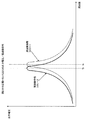
図2は、図1の電源装置80における詳細な構成例を示す回路図である。更に、図5は、図2中の圧電トランス220における出力電圧/周波数の特性図である。   FIG. 2 is a circuit diagram showing a detailed configuration example of the power supply device 80 of FIG. 5 is a characteristic diagram of output voltage / frequency in the piezoelectric transformer 220 in FIG.

図2では、説明を簡単にするために、高圧制御部100において、4チャンネルの入力ポートIN12C,IN12M,IN12Y,IN12Kのうちの1チャンネル分の入力ポートIN12と、4チャンネルの入力ポートIN13C,IN13M,IN13Y,IN13Kのうちの1チャンネル分の入力ポートIN13と、4チャンネルの出力ポートOUT11C,OUT11M,OUT11Y,OUT11Kのうちの1チャンネル分の出力ポートOUT11と、4チャンネルの出力ポートOUT12C,OUT12M,OUT12Y,OUT12Kのうちの1チャンネル分の出力ポートOUT12と、4チャンネルの出力ポートOUT13C,OUT13M,OUT13Y,OUT13Kのうちの1チャンネル分の出力ポートOUT13とが図示されている。更に、4チャンネルの同一回路構成の圧電トランス高圧回路200C,200M,200Y,200Kのうちの1チャンネル分の圧電トランス高圧回路200が図示されている。   In FIG. 2, in order to simplify the description, in the high voltage controller 100, the input port IN12 for one channel among the four channel input ports IN12C, IN12M, IN12Y, IN12K, and the four channel input ports IN13C, IN13M. , IN13Y, IN13K for one channel input port IN13, four channel output ports OUT11C, OUT11M, OUT11Y, OUT11K for one channel output port OUT11, and four channel output ports OUT12C, OUT12M, OUT12Y , OUT12K for one channel output port OUT12 and four channel output ports OUT13C, OUT13M, OUT13Y, OUT13K for one channel output port OUT13. There has been shown. Furthermore, the piezoelectric transformer high-voltage circuit 200 for one channel among the piezoelectric transformer high-voltage circuits 200C, 200M, 200Y, and 200K having the same circuit configuration of four channels is illustrated.

図2に示すように、プリンタエンジン制御部60のシリアル通信手段61と、高圧制御部100のシリアル通信手段101とは、3本の信号線(例えば、SCLK1線、SDI1線、及びSDO1線)により接続されている。   As shown in FIG. 2, the serial communication unit 61 of the printer engine control unit 60 and the serial communication unit 101 of the high voltage control unit 100 are connected by three signal lines (for example, SCLK1 line, SDI1 line, and SDO1 line). It is connected.

SCLK1線は、後述する転送データに同期したクロックをプリンタエンジン制御部60から高圧制御部100へ出力するシリアルクロックSCLK1の信号線である。SDI1線は、高圧制御部100にデータを入力するシリアルデータインプット信号SDI1であって、シリアルクロックSCLK1に同期してデータをプリンタエンジン制御部60から高圧制御部100へ送信する信号線である。更に、SDO1線は、高圧制御部100からシリアルクロックSCLK1に同期して出力されるシリアルデータアウトプット信号SDO1であって、シリアルクロックSCLK1に同期してデータを送信する信号線である。 The SCLK1 line is a signal line of the serial clock SCLK1 that outputs a clock synchronized with transfer data, which will be described later, from the printer engine control unit 60 to the high voltage control unit 100. The SDI1 line is a serial data input signal SDI1 for inputting data to the high voltage controller 100, and is a signal line for transmitting data from the printer engine controller 60 to the high voltage controller 100 in synchronization with the serial clock SCLK1. The SDO1 line is a serial data output signal SDO1 output from the high voltage controller 100 in synchronization with the serial clock SCLK1, and is a signal line for transmitting data in synchronization with the serial clock SCLK1.

この3線式のシリアル通信は、公知の通信であるので詳細は省く。画像形成装置1の高圧出力のオン/オフ(以下「ON/OFF」という。)タイミングの精度はmsecオーダであるので、シリアル通信によるμsecオーダでの通信速度であっても問題はない。   Since this three-wire serial communication is a known communication, details are omitted. Since the accuracy of ON / OFF (hereinafter referred to as “ON / OFF”) timing of the high-voltage output of the image forming apparatus 1 is on the order of msec, there is no problem even if the communication speed is on the order of μsec by serial communication.

高圧制御部100にクロックCLKを供給する発振器90は、電源91から供給されるDC3.3Vにより動作して発振周波数50MHzのクロックCLKを発生する回路であり、DC3.3Vが印加される電源端子VDD、DC3.3Vが印加される出力イネーブル端子OE、クロックCLKを出力するクロック出力端子CLK_OUT、及び接地されたグランド端子GNDを有している。クロック出力端子CLK_OUTは、抵抗92を介して、高圧制御部100のクロック入力ポートCLK_INに接続されている。   The oscillator 90 that supplies the clock CLK to the high-voltage controller 100 is a circuit that operates by DC 3.3V supplied from the power supply 91 and generates the clock CLK having an oscillation frequency of 50 MHz. The power supply terminal VDD to which DC 3.3V is applied. , An output enable terminal OE to which DC 3.3 V is applied, a clock output terminal CLK_OUT for outputting the clock CLK, and a ground terminal GND. The clock output terminal CLK_OUT is connected to the clock input port CLK_IN of the high voltage controller 100 via the resistor 92.

クロックCLKに同期して動作する高圧制御部100において、駆動パルスS100を出力する出力ポートOUT11には、圧電トランス高圧回路200内の抵抗201を介して、圧電トランス駆動回路210が接続され、この圧電トランス駆動回路210にDC電源95が接続されている。DC電源95は、例えば、図示しない低圧電源装置から商用電源であるAC100Vを変圧整流することにより供給されるDC24Vの電源である。   In the high-voltage control unit 100 that operates in synchronization with the clock CLK, the piezoelectric transformer drive circuit 210 is connected to the output port OUT11 that outputs the drive pulse S100 via the resistor 201 in the piezoelectric transformer high-voltage circuit 200. A DC power source 95 is connected to the transformer driving circuit 210. The DC power source 95 is, for example, a DC 24V power source that is supplied by transforming and rectifying AC 100V, which is a commercial power source, from a low-voltage power device (not shown).

圧電トランス駆動回路210は、スイッチング素子であるパワートランジスタ(例えば、NチャネルパワーMOSFET(以下「NMOS」という。)211を有し、このNMOS211のゲート・ソース間に、短絡防止用の抵抗212が接続されている。NMOS211のドレインは、インダクタ(コイル)213を介してDC24VのDC電源95に接続されている。NMOS211のドレイン・ソース間には、コンデンサ214が並列に接続され、このコンデンサ214及びインダクタ213により共振回路が構成されている。NMOS211のゲートに、高圧制御部100からの駆動パルスS100が入力されると、このNMOS211によりDC24Vがスイッチングされ、これが共振回路により共振されてピークがAC100V程度の正弦半波の駆動電圧が出力される。   The piezoelectric transformer driving circuit 210 includes a power transistor (for example, an N-channel power MOSFET (hereinafter referred to as “NMOS”) 211 as a switching element, and a resistor 212 for preventing a short circuit is connected between the gate and source of the NMOS 211. The drain of the NMOS 211 is connected to a DC power source 95 of 24 V DC via an inductor (coil) 213. A capacitor 214 is connected in parallel between the drain and source of the NMOS 211, and the capacitor 214 and the inductor. A resonance circuit is configured by 213. When the drive pulse S100 from the high voltage controller 100 is input to the gate of the NMOS 211, DC 24V is switched by the NMOS 211, which is resonated by the resonance circuit, and the peak is AC 100V. Driving voltage of the sinusoidal half wave of each time is output.

共振回路の出力側には、圧電トランス220の1次側の入力端子221が接続され、この2次側の出力端子222から、NMOS211のスイッチング周波数に応じて0〜数kVのAC高電圧が出力される構成になっている。2次側の出力端子222の出力電圧特性は、図5に示すように、周波数によって異なり、NMOS211のスイッチング周波数により昇圧比が決定される。   The primary side input terminal 221 of the piezoelectric transformer 220 is connected to the output side of the resonance circuit, and an AC high voltage of 0 to several kV is output from the secondary side output terminal 222 according to the switching frequency of the NMOS 211. It is configured to be. As shown in FIG. 5, the output voltage characteristic of the output terminal 222 on the secondary side varies depending on the frequency, and the step-up ratio is determined by the switching frequency of the NMOS 211.

即ち、圧電トランス220の出力電圧/周波数特性は、図5に示すように、ある圧電トランス220−1においては、周波数fxで出力電圧が極大値を取り、別の圧電トランス220−2においては、周波数fyで出力電圧が極大値を取る。このように、圧電トランス220−1,220−2の製造ばらつきによって、異なる周波数特性を有している。これは、製造時の圧電トランス220の大きさにばらつきが生じるためであり、ばらつきの範囲は例えば周波数にして±4%程度である。本実施例1において、出力電圧の制御は、周波数が高い図5の右側の特性を有する周波数で圧電トランス220を駆動し、駆動周波数を下げていくことにより、出力電圧を上昇させ、結果、出力電流も増大させ、目標の出力電流を得るような制御を行う構成になっている。   That is, as shown in FIG. 5, the output voltage / frequency characteristic of the piezoelectric transformer 220 has a maximum output voltage at a frequency fx in one piezoelectric transformer 220-1, and in another piezoelectric transformer 220-2, The output voltage takes a maximum value at the frequency fy. As described above, the piezoelectric transformers 220-1 and 220-2 have different frequency characteristics due to manufacturing variations. This is because variation occurs in the size of the piezoelectric transformer 220 at the time of manufacture, and the range of variation is, for example, about ± 4% in terms of frequency. In the first embodiment, the output voltage is controlled by driving the piezoelectric transformer 220 at a frequency having a high frequency in the right side of FIG. 5 and lowering the drive frequency, thereby increasing the output voltage, resulting in an output. The control is performed to increase the current and obtain a target output current.

圧電トランス220の2次側の出力端子222には、AC/DC変換用の整流回路230が接続されている。整流回路230は、圧電トランス220の2次側の出力端子222から出力されたAC高電圧をDC高電圧に変換して出力する回路であり、ダイオード231,232及びコンデンサ233により構成されている。整流回路230の出力側には、抵抗234を介して出力負荷ZLである転写ローラ5が接続されると共に、出力電圧変換手段240が接続されている。   A rectifier circuit 230 for AC / DC conversion is connected to the output terminal 222 on the secondary side of the piezoelectric transformer 220. The rectifier circuit 230 is a circuit that converts an AC high voltage output from the output terminal 222 on the secondary side of the piezoelectric transformer 220 into a DC high voltage and outputs the DC high voltage, and includes a diode 231 and 232 and a capacitor 233. To the output side of the rectifier circuit 230, the transfer roller 5 as an output load ZL is connected via a resistor 234, and an output voltage conversion means 240 is connected.

出力電圧変換手段240は、整流回路230から出力されたDC高電圧(例えば、DC0〜7000V)を分圧してDC低電圧(例えば、DC0〜3.3V)を出力する回路であり、DC高電圧を分圧する分圧抵抗241(例えば、100MΩ)及び分圧抵抗242(例えば、47kΩ)と、CRフィルタを構成する抵抗243及びコンデンサ244とを有している。CRフィルタを構成する抵抗243及びコンデンサ244は、出力電圧のリップル成分を低減する機能を有している。出力電圧変換手段240の出力側には、第1及び第2の電圧比較手段270,280が接続されている。   The output voltage conversion means 240 is a circuit that divides the DC high voltage (for example, DC 0 to 7000 V) output from the rectifier circuit 230 and outputs the DC low voltage (for example, DC 0 to 3.3 V). Voltage dividing resistor 241 (for example, 100 MΩ) and voltage dividing resistor 242 (for example, 47 kΩ), and a resistor 243 and a capacitor 244 constituting a CR filter. The resistor 243 and the capacitor 244 constituting the CR filter have a function of reducing the ripple component of the output voltage. First and second voltage comparison means 270 and 280 are connected to the output side of the output voltage conversion means 240.

高圧制御部100の出力ノードOUT13には、信号線(例えば、シリアルクロックSCLK2用信号線、及びシリアルデータSDO2用信号線)を介してDAC250が接続されている。DAC250は、出力ノードOUT13からシリアルクロックSCLK2に同期して出力されるシリアルデータSDO2を、分解能10bitでアナログ信号に変換し、4チャンネルの出力電圧S250(例えば、0〜3.3V)を三角波発生手段260及び第1の電圧比較手段270へ出力する回路である。   The DAC 250 is connected to the output node OUT13 of the high-voltage controller 100 via signal lines (for example, a signal line for serial clock SCLK2 and a signal line for serial data SDO2). The DAC 250 converts serial data SDO2 output from the output node OUT13 in synchronization with the serial clock SCLK2 into an analog signal with a resolution of 10 bits, and generates a 4-channel output voltage S250 (for example, 0 to 3.3 V) as a triangular wave generating means. 260 and a circuit for outputting to the first voltage comparison means 270.

三角波発生手段260は、演算増幅器(以下「オペアンプ」という。)261及び抵抗262−1,262−2で構成される負帰還増幅回路と、プルアップ抵抗262−3〜262−6と、NPNトランジスタ(以下「NPNTR」という。)263−1〜263−4と、抵抗264−1〜264−4及び抵抗264−5〜264−9で構成されるR2R回路と、NPNTR263−1〜263−4のベース抵抗266−1〜266−4と、出力側の抵抗264−10及びコンデンサ265とを有する回路である。   The triangular wave generating means 260 includes a negative feedback amplifier circuit composed of an operational amplifier (hereinafter referred to as “op-amp”) 261 and resistors 262-1 and 262-2, pull-up resistors 262-2 to 262-6, and an NPN transistor. (Hereinafter referred to as “NPNTR”) 263-1 to 263-4, R2R circuit composed of resistors 264-1 to 264-4 and resistors 264-5 to 264-9, and NPNTR 263-1 to 263-4 This circuit includes base resistors 266-1 to 266-4, an output-side resistor 264-10, and a capacitor 265.

この三角波発生手段260では、DAC250の出力電圧S250がオペアンプ261の+入力端子に入力され、このオペアンプ261及び抵抗262−1,262−2によって構成される負帰還増幅回路により、4倍の電圧に増幅される。増幅された電圧は、プルアップ抵抗262−3〜262−6でプルアップされ、NPNTR263−1〜263−4のコレクタがプルアップされる。プルアップされた電圧は、抵抗264−1〜264−4及び抵抗264−5〜264−9で構成されるR2R回路(即ち、前者の抵抗264−1〜264−4と後者の抵抗264−5〜264−9それぞれ等しい抵抗値にて前者と後者の抵抗値比が2:1である回路)に供給される。供給される電圧は、高圧制御部100における4チャンネルの出力ノードOUT12から出力される信号により、抵抗266−1〜266−4を介してNPNTR263−1〜263−4のベースがオン/オフされることにより切り替えられる。このR2R回路により、0VからDAC250の出力電圧S250の2倍の電圧範囲の三角波S260を、4bit分解能(即ち、0〜15段階)で、第2の電圧比較手段280へ出力できるようになっている。   In this triangular wave generating means 260, the output voltage S250 of the DAC 250 is input to the + input terminal of the operational amplifier 261, and the negative feedback amplifier circuit composed of the operational amplifier 261 and the resistors 262-1 and 262-2 increases the voltage to 4 times. Amplified. The amplified voltage is pulled up by the pull-up resistors 262-2 to 262-6, and the collectors of the NPNTRs 263-1 to 263-4 are pulled up. The pulled-up voltage is an R2R circuit composed of resistors 264-1 to 264-4 and resistors 264-5 to 264-9 (that is, the former resistors 264-1 to 264-4 and the latter resistors 264-5). ... 264-9 are supplied to a circuit having a resistance value ratio of 2: 1 between the former and the latter with equal resistance values. As for the supplied voltage, the bases of the NPNTRs 263-1 to 263-4 are turned on / off via the resistors 266-1 to 266-4 by a signal output from the 4-channel output node OUT <b> 12 in the high-voltage control unit 100. Can be switched. By this R2R circuit, a triangular wave S260 having a voltage range from 0V to twice the output voltage S250 of the DAC 250 can be output to the second voltage comparison means 280 with 4-bit resolution (ie, 0 to 15 steps). .

出力電圧変換手段240の出力側に接続された第1、第2の電圧比較手段270,280のうち、第1の電圧比較手段270は、コンパレータ271及びプルアップ抵抗272を有している。コンパレータ271は、この+入力端子がDAC250の出力端子に接続され、−入力端子が出力電圧変換手段240の出力端子に接続されている。コンパレータ271の出力端子は、プルアップ抵抗272を介して、DC3.3Vの電源91に接続されている。コンパレータ271は、+入力端子に入力される出力電圧S250と、−入力端子に入力される出力電圧S240とを比較し、+入力端子側の出力電圧S250が−入力端子側の出力電圧S240より高い場合にオープンコレクタ出力となって、抵抗272によりプルアップされた比較結果S270(=3.3VのHレベル)を出力し、−入力端子側の出力電圧S240が+入力端子側の出力電圧S250より高い場合に比較結果S270(=Lレベル)を出力し、高圧制御部100における入力ポートIN12に入力するようになっている。   Of the first and second voltage comparison means 270 and 280 connected to the output side of the output voltage conversion means 240, the first voltage comparison means 270 has a comparator 271 and a pull-up resistor 272. The comparator 271 has its + input terminal connected to the output terminal of the DAC 250 and its − input terminal connected to the output terminal of the output voltage conversion means 240. The output terminal of the comparator 271 is connected to a DC 3.3V power source 91 via a pull-up resistor 272. The comparator 271 compares the output voltage S250 input to the + input terminal with the output voltage S240 input to the − input terminal, and the output voltage S250 on the + input terminal side is higher than the output voltage S240 on the − input terminal side. The comparison result S270 (= 3.3V H level) pulled up by the resistor 272 is output, and the negative input terminal side output voltage S240 is more than the positive input terminal side output voltage S250. When the value is high, the comparison result S270 (= L level) is output and input to the input port IN12 in the high voltage control unit 100.

第2の電圧比較手段280は、コンパレータ281及びプルアップ抵抗282を有している。コンパレータ281は、この+入力端子が、抵抗264−10を介して抵抗264−5,264−6に接続されると共に、コンデンサ265を介してグランドGNDに接続され、−入力端子が、出力電圧変換手段240の出力端子に接続されている。コンパレータ280の出力端子は、プルアップ抵抗272を介して、DC3.3Vの電源91に接続されている。コンパレータ281は、+入力端子に入力される三角波S260の電圧と、−入力端子に入力される出力電圧S240とを比較し、+入力端子側の三角波S260の電圧が−入力端子側の出力電圧S240より高い場合にオープンコレクタ出力となって、抵抗282によりプルアップされた比較結果S280(=3.3VのHレベル)を出力し、−入力端子側の出力電圧S240が+入力端子側の三角波S260の電圧より高い場合に比較結果S280(=Lレベル)を出力し、高圧制御部100における入力ポートIN13に入力するようになっている。   The second voltage comparison means 280 has a comparator 281 and a pull-up resistor 282. In the comparator 281, the + input terminal is connected to the resistors 264-5 and 264-6 through the resistor 264-10 and is connected to the ground GND through the capacitor 265, and the − input terminal is converted to the output voltage. Connected to the output terminal of means 240. The output terminal of the comparator 280 is connected to the DC 3.3 V power source 91 via the pull-up resistor 272. The comparator 281 compares the voltage of the triangular wave S260 input to the + input terminal with the output voltage S240 input to the − input terminal, and the voltage of the triangular wave S260 on the + input terminal side becomes the output voltage S240 on the − input terminal side. When the output voltage is higher, the output becomes an open collector output, and the comparison result S280 (= 3.3V H level) pulled up by the resistor 282 is output. The output voltage S240 on the −input terminal side is the triangular wave S260 on the + input terminal side. The comparison result S280 (= L level) is output when the voltage is higher than the input voltage, and is input to the input port IN13 in the high voltage controller 100.

(電源装置内の制御部の構成)
図6は、図2中の高圧制御部100を示す構成図である。
(Configuration of control unit in power supply)
FIG. 6 is a configuration diagram showing the high-voltage control unit 100 in FIG.

高圧制御部100は、例えば、ASICにより構成されており、ハードウェア記述言語等により記述されてASIC化されている。   The high-voltage control unit 100 is configured by, for example, an ASIC, and is described as an ASIC by being described in a hardware description language or the like.

高圧制御部100は、50MHzのクロックCLKが入力される256分周器102を有している。256分周器102は、50MHzのクロックCLKを256分周し、195.3kHz、5.12μsec周期のパルスを5bitカウンタ103及び4チャンネルの5bitカウンタ106へそれぞれ出力する回路である。5bitカウンタ103は、前記5.12μsec周期のパルスをカウントする5bitのカウンタであり、最上位bit(以下「MSB」という。)を選択信号としてセレクタ105へ出力し、下位4bitをそのセレクタ105と否定ゲート(以下「NOTゲート」という。)104に入力し、更に、オーバフロー時に論理Hをデータラッチ回路(以下「Dラッチ」という。)107−1へ出力し、それ以外では論理Lを出力する回路である。   The high-voltage control unit 100 includes a 256 frequency divider 102 to which a 50 MHz clock CLK is input. The 256 frequency divider 102 is a circuit that divides the frequency of the 50 MHz clock CLK by 256 and outputs pulses of 195.3 kHz and 5.12 μsec to the 5-bit counter 103 and the 4-bit 5-bit counter 106, respectively. The 5-bit counter 103 is a 5-bit counter that counts the pulses having the cycle of 5.12 μsec, outputs the most significant bit (hereinafter referred to as “MSB”) to the selector 105 as a selection signal, and negates the lower 4 bits from the selector 105. A circuit that inputs to a gate (hereinafter referred to as "NOT gate") 104, and further outputs a logic H to a data latch circuit (hereinafter referred to as "D latch") 107-1 upon overflow, and outputs a logic L otherwise. It is.

NOTゲート104は、5bitカウンタ103から入力された4bitをH/L反転させてセレクタ105へ出力する回路である。セレクタ105は、5bitカウンタ103のMSBが選択信号として入力され、5bitカウンタ103の下位4bit又はNOTゲート104の出力4bitを4チャンネルの出力ポートOUT12へ出力する回路である。5bitカウンタ106は、入力ポートIN13から入力される4チャンネルの比較結果S280のH期間を256分周器102の出力パルスにてカウントし、又、5bitカウンタ103から出力されるオーバフロー信号でカウント値が0にクリア(CLR)されるカウンタであり、この出力側にDラッチ107−1が接続されている。Dラッチ107−1は、5bitカウンタ103のオーバフロー信号(SET)により、5bitカウンタ106の出力5bitをラッチする回路であり、この出力側にセレクタ110−1が接続されている。   The NOT gate 104 is a circuit that inverts H / L of 4 bits input from the 5-bit counter 103 and outputs the result to the selector 105. The selector 105 is a circuit that receives the MSB of the 5-bit counter 103 as a selection signal and outputs the lower 4 bits of the 5-bit counter 103 or the output 4 bits of the NOT gate 104 to the 4-channel output port OUT12. The 5-bit counter 106 counts the H period of the 4-channel comparison result S280 input from the input port IN13 by the output pulse of the 256 frequency divider 102, and the count value is counted by the overflow signal output from the 5-bit counter 103. The counter is cleared (CLR) to 0, and the D latch 107-1 is connected to the output side. The D latch 107-1 is a circuit that latches the output 5 bits of the 5-bit counter 106 by the overflow signal (SET) of the 5-bit counter 103, and the selector 110-1 is connected to this output side.

セレクタ110−1は、タイマ116から出力される2bitデータに応じて、4チャンネルのDラッチ107−1の出力5bitのうち1チャンネルの出力5bitをテーブルレジスタ111−1へ出力する回路である。テーブルレジスタ111−1は、セレクタ110−1の出力5bitとテーブルレジスタ111−3の出力2bitとの値に応じて、8bit値を乗算器112へ出力する回路である。テーブルレジスタ111−3は、セレクタ110−2の出力7bitが入力され、この出力7bit値に応じた出力2bitをテーブルレジスタ111−1へ出力する回路である。セレクタ110−2の出力側には、テーブルレジスタ111−2も接続されている。テーブルレジスタ111−2は、セレクタ110−2の出力7bitが入力され、この出力7bit値に応じた出力8bitを乗算器112へ出力する回路である。この乗算器112の入力側に接続されたテーブルレジスタ111−1〜111−3等は、周波数制御値の可変幅を変更する変更手段を構成している。   The selector 110-1 is a circuit that outputs 5 bits of 1 channel out of 5 bits of the output of the D latch 107-1 of 4 channels to the table register 111-1 according to 2 bits of data output from the timer 116. The table register 111-1 is a circuit that outputs an 8-bit value to the multiplier 112 in accordance with the value of the output 5 bits of the selector 110-1 and the output 2 bits of the table register 111-3. The table register 111-3 is a circuit that receives the 7-bit output of the selector 110-2 and outputs an output 2 bits corresponding to the output 7-bit value to the table register 111-1. A table register 111-2 is also connected to the output side of the selector 110-2. The table register 111-2 is a circuit that receives the 7-bit output of the selector 110-2 and outputs an 8-bit output corresponding to the output 7-bit value to the multiplier 112. The table registers 111-1 to 111-3 connected to the input side of the multiplier 112 constitute changing means for changing the variable width of the frequency control value.

乗算器112は、テーブルレジスタ111−1の出力8bitと、テーブルレジスタ111−2の出力8bitとを乗算し、16bitの乗算結果を演算器114−1へ出力する回路である。この乗算器112及び演算器114−1により、駆動パルスS100の駆動周波数を決定する周波数制御値を制御するスイッチング制御手段を構成している。   The multiplier 112 is a circuit that multiplies the output 8 bits of the table register 111-1 and the output 8 bits of the table register 111-2, and outputs a 16-bit multiplication result to the arithmetic unit 114-1. The multiplier 112 and the calculator 114-1 constitute a switching control means for controlling a frequency control value that determines the drive frequency of the drive pulse S100.

4チャンネルの比較結果S270が入力される入力ポートIN12には、9bitカウンタ108が接続されている。9bitカウンタ108は、入力ポートIN12から入力される4チャンネルの比較結果S270のH期間を、50MHzのクロックCLKにてカウントし、又、駆動パルスS100の立ち上がりエッジでクリアされる回路であり、この出力側にDラッチ107−2が接続されている。Dラッチ107−2は、入力ポートIN11から入力されるリセット信号RESETにより0にクリア(CLR)され、駆動パルスS100の立ち上がりエッジで、9bitカウンタ108の出力9bitをラッチする回路である。   A 9-bit counter 108 is connected to the input port IN12 to which the 4-channel comparison result S270 is input. The 9-bit counter 108 is a circuit that counts the H period of the 4-channel comparison result S270 input from the input port IN12 with the 50 MHz clock CLK, and is cleared at the rising edge of the drive pulse S100. The D latch 107-2 is connected to the side. The D latch 107-2 is a circuit that is cleared to 0 (CLR) by a reset signal RESET input from the input port IN11 and latches the output 9 bits of the 9-bit counter 108 at the rising edge of the drive pulse S100.

シリアル通信手段101及び出力ポートOUT13には、通信データ処理部109が接続されている。通信データ処理部109は、シリアル通信手段101によるデータに応じて出力する4チャンネルのON/OFF信号S109とシリアルクロックSCLK1及びシリアルデータSDA1とを制御して、DAC250から出力される4チャンネルの出力電圧S250を制御するものである。   A communication data processing unit 109 is connected to the serial communication unit 101 and the output port OUT13. The communication data processing unit 109 controls the 4-channel ON / OFF signal S109, the serial clock SCLK1, and the serial data SDA1 that are output according to the data from the serial communication unit 101, and the 4-channel output voltage output from the DAC 250. S250 is controlled.

Dラッチ107−2の出力側には、4チャンネルの比較器113が接続されている。比較器113は、Dラッチ107−2の出力9bitと、19bitレジスタ119−2の上位9bit出力値とを比較し、2bit出力値を下記のようにして演算器114−1へ出力する。   A 4-channel comparator 113 is connected to the output side of the D latch 107-2. The comparator 113 compares the 9-bit output of the D-latch 107-2 with the higher-order 9-bit output value of the 19-bit register 119-2, and outputs the 2-bit output value to the computing unit 114-1.

(Dラッチ107−2の値)≧(19bitレジスタ119−2の上位9bit値−5)の場合に00bを出力し、
(19bitレジスタ119−2の上位9bit値−5)>(Dラッチ107−2の値)≧(19bitレジスタ119−2の上位9bit値×0.5)の場合に01bを出力し、
(19bitレジスタ119−2の上位9bit値×0.5)>(Dラッチ107−2の値)>5の場合に10bを出力し、
5≧(Dラッチ107−2の値)の場合に11bを出力する。
When (value of D latch 107-2) ≧ (higher 9-bit value of 19-bit register 119-2−5), 00b is output,
If (the upper 9-bit value of the 19-bit register 119-2 −5)> (the value of the D latch 107-2) ≧ (the upper 9-bit value of the 19-bit register 119-2 × 0.5), 01b is output,
When (the upper 9-bit value of the 19-bit register 119-2 × 0.5)> (value of the D latch 107-2)> 5, 10b is output,
If 5 ≧ (value of D latch 107-2), 11b is output.

セレクタ110−2及び演算器114−1には、タイマ116を介して周期値記憶用メモリ115が接続されている。周期値記憶用メモリ115は、制御周期を決定する13bitの周期値(例えば、140μsecに相当する値である7000(1B58hex))を記憶するフラッシュメモリ等のメモリである。周期値は、50MHzのクロックCLKの誤差に応じて可変設定可能な値となっている。タイマ116は、13bitのカウンタを備え、0000〜07FF、0800〜0FFF、1000〜17FF、1800〜1FFFへとカウントアップする間に、セレクタ110−1及び110−2への2bit出力値を00、01、10、11bと変化させ、2bit値を変化させた所定時間後に4bitのパルスを順次演算器114−1へ出力し、更に、カウントアップした値が前記516周期値と等しくなった時に13bit値に0000hexをセットする回路である。   A cycle value storage memory 115 is connected to the selector 110-2 and the arithmetic unit 114-1 via a timer 116. The cycle value storage memory 115 is a memory such as a flash memory that stores a 13-bit cycle value (for example, 7000 (1B58 hex) corresponding to 140 μsec) that determines the control cycle. The period value is a value that can be variably set according to the error of the clock CLK of 50 MHz. The timer 116 includes a 13-bit counter, and outputs the 2-bit output value to the selectors 110-1 and 110-2 to 00, 01 while counting up to 0000-07FF, 0800-0FFF, 1000-17FF, 1800-1FFF. 10 and 11b, a 4-bit pulse is sequentially output to the calculator 114-1 after a predetermined time after changing the 2-bit value, and when the counted up value becomes equal to the 516 period value, the 13-bit value is obtained. This circuit sets 0000 hex.

演算器114−1には、9bitのカウンタ上限値レジスタ117、9bitのカウンタ下限値レジスタ118、及び19bitレジスタ119−1が接続されている。19bitレジスタ119−1は、駆動パルスS100における駆動周波数の初期値と、駆動周波数を決定する周波数制御値とを記憶する記憶手段としての機能を有している。演算器114−1は、19bitレジスタ119−1の19bit値が入力され、この値に対して演算を行い、演算結果を19bitレジスタ119−1へ出力して更新する機能を有している。   The arithmetic unit 114-1 is connected to a 9-bit counter upper limit register 117, a 9-bit counter lower limit register 118, and a 19-bit register 119-1. The 19-bit register 119-1 has a function as a storage unit that stores an initial value of the drive frequency in the drive pulse S100 and a frequency control value that determines the drive frequency. The computing unit 114-1 has a function of inputting the 19-bit value of the 19-bit register 119-1, performing an operation on this value, outputting the operation result to the 19-bit register 119-1 and updating it.

演算器114−1における演算は、リセット信号RESETの入力時、カウンタ下限値レジスタ118の9bit値に、下位10bitに0をセットした値が設定され、比較器113の出力2bitに応じて乗算器112の出力値もしくは1を加減算する。加減算結果の上位9bitがカウンタ上限値レジスタ117の9bit値を超えた場合には、上位9bit値をカウンタ上限値レジスタ117の値として下位10bitを0とし、カウンタ下限値レジスタ118の9bit値を下回った場合には、上位9bit値をカウンタ下限値レジスタ118の値として下位10bitを0とする。比較器113の出力2bit値と演算の関係は、以下の通りである。本実施例1では、下限値は180hex、上限値は1CFhexである。
比較器113の出力値00b:乗算器112の出力値16bitを加算
比較器113の出力値01b:乗算器112の出力値1を加算
比較器113の出力値10b:乗算器112の出力値1を減算
比較器113の出力値11b:乗算器112の出力値16bitを減算
When the reset signal RESET is input, the arithmetic unit 114-1 sets the 9-bit value of the counter lower limit register 118 to a value in which 0 is set to the lower 10 bits, and the multiplier 112 according to the output 2 bits of the comparator 113. The output value or 1 is added or subtracted. When the upper 9 bits of the addition / subtraction result exceeds the 9 bit value of the counter upper limit register 117, the upper 9 bit value is set to the counter upper limit register 117, the lower 10 bits are set to 0, and the counter lower limit register 118 is lower than the 9 bit value. In this case, the upper 9-bit value is set to the value of the counter lower limit register 118, and the lower 10-bit is set to 0. The relationship between the output 2-bit value of the comparator 113 and the calculation is as follows. In the first embodiment, the lower limit value is 180 hex, and the upper limit value is 1 CF hex.
Output value 00b of the comparator 113: Add 16-bit output value of the multiplier 112 Output value 01b of the comparator 113: Add output value 1 of the multiplier 112 Output value 10b of the comparator 113: Output value 1 of the multiplier 112 Subtraction Output value 11b of comparator 113: Subtracts 16-bit output value of multiplier 112

19bitレジスタ119−1は、演算器114−1の出力19bit値をラッチして保持する機能を有し、この19bitレジスタ119−1と保持手段である補正値レジスタ120とに、演算器114−2が接続されている。補正値レジスタ120は、8bitのレジスタであり、4チャンネル分の各チャンネルの補正値を符号付き値として保持する機能を有している。演算器114−2は、19bitレジスタ119−1で、補正値レジスタ120の出力8bitを19bitのbit18−0のうちbit13−7に対して加減算するものである。例えば、19bitレジスタ119−1の出力値が60000hexで、補正値レジスタ120の値が01hexの場合は、60080hexとなり、補正値レジスタ120の値がFFhexの場合は、5FF80hexとなる。   The 19-bit register 119-1 has a function of latching and holding the output 19-bit value of the computing unit 114-1. Is connected. The correction value register 120 is an 8-bit register, and has a function of holding correction values of four channels for each channel as signed values. The computing unit 114-2 is a 19-bit register 119-1 that adds / subtracts the output 8 bits of the correction value register 120 to / from bit 13-7 of the 19-bit bits 18-0. For example, when the output value of the 19-bit register 119-1 is 60000 hex and the value of the correction value register 120 is 01 hex, the value is 60080 hex, and when the value of the correction value register 120 is FF hex, the value is 5FF 80 hex.

演算器114−2には、19bitレジスタ119−2が接続され、この19bitレジスタ119−2に、比較器113、1加算器121、分周セレクタ122、及び誤差保持レジスタ125が接続されている。分周セレクタ122及び誤差保持レジスタ125は、誤差拡散法による2値化手段を構成している。更に、分周セレクタ122には、分周手段である分周器123が接続され、この分周器123に、出力セレクタ124及び誤差保持レジスタ125が接続されている。   A 19-bit register 119-2 is connected to the arithmetic unit 114-2, and a comparator 113, an adder 121, a frequency divider selector 122, and an error holding register 125 are connected to the 19-bit register 119-2. The frequency divider selector 122 and the error holding register 125 constitute a binarization unit using an error diffusion method. Furthermore, a frequency divider 123 that is a frequency dividing means is connected to the frequency divider selector 122, and an output selector 124 and an error holding register 125 are connected to the frequency divider 123.

19bitレジスタ119−2は、演算器114−2の出力19bit値をラッチして保持し、上位9bitを1加算器121と分周セレクタ122へ出力し、下位10bitを誤差保持レジスタ125へ出力する回路である。誤差保持レジスタ125は、10bitのレジスタと1bitのフラグとにより構成され、リセット信号RESETの入力で10bit値及びフラグ1bit共に0にクリアされ、19bitレジスタ119−2の出力10bit値を、分周器123の出力パルスの立ち上がりエッジでレジスタ値に加算して保持し、更に、加算時にオーバフローが発生した場合には、フラグ1bitを1とし、そうでない場合は、フラグ1bitを0とするレジスタである。   The 19-bit register 119-2 latches and holds the output 19-bit value of the arithmetic unit 114-2, outputs the upper 9 bits to the 1 adder 121 and the frequency divider selector 122, and outputs the lower 10 bits to the error holding register 125. It is. The error holding register 125 is composed of a 10-bit register and a 1-bit flag. When the reset signal RESET is input, both the 10-bit value and the flag 1-bit are cleared to 0, and the output 10-bit value of the 19-bit register 119-2 is divided into the frequency divider 123. The register is added to the register value at the rising edge of the output pulse and held, and when overflow occurs during addition, the flag 1 bit is set to 1; otherwise, the flag 1 bit is set to 0.

1加算器121は、19bitレジスタ119−2の出力9bit値に1加算した9bit値を、分周セレクタ122へ出力するものである。分周セレクタ122は、誤差保持レジスタ125の出力1bitが選択信号selectとして与えられ、この選択信号selectにより、19bitレジスタ119−2の出力9bitと1加算器121の出力9bitとを切り替える回路である。この分周セレクタ122は、選択信号selectがHの場合には、1加算器121の出力値を分周器123へ出力し、選択信号selectがLの場合には、19bitレジスタ119−2の出力値を分周器123へ出力する。   The 1 adder 121 outputs a 9-bit value obtained by adding 1 to the output 9-bit value of the 19-bit register 119-2 to the frequency division selector 122. The frequency divider selector 122 is a circuit that receives the 1-bit output of the error holding register 125 as a selection signal select, and switches between the 9-bit output of the 19-bit register 119-2 and the 9-bit output of the 1 adder 121 in accordance with the selection signal select. The frequency divider selector 122 outputs the output value of the 1 adder 121 to the frequency divider 123 when the selection signal select is H, and the output of the 19-bit register 119-2 when the selection signal select is L. The value is output to the frequency divider 123.

分周器123は、分周セレクタ122から出力される9bit値のカウントのパルスをデューティ30%で出力セレクタ124へ出力する回路である。出力セレクタ124は、通信データ処理部109から出力されるON/OFF信号S109がHの場合に、分周器123から入力される駆動パルスS100を出力し、ON/OFF信号S109がLの場合に、グランド電位のLを出力する機能を有している。   The frequency divider 123 is a circuit that outputs a 9-bit count pulse output from the frequency divider selector 122 to the output selector 124 with a duty of 30%. The output selector 124 outputs the drive pulse S100 input from the frequency divider 123 when the ON / OFF signal S109 output from the communication data processing unit 109 is H, and when the ON / OFF signal S109 is L. , And has a function of outputting L of the ground potential.

(画像形成装置の全体の動作)
図3及び図4において、画像形成装置1は、図示しない外部機器からホストインタフェース部51を介してPDL(Page Description Language、ページ記述言語)等で記述された印刷データが入力されると、この印刷データは、コマンド/画像処理部52によってビットマップデータ(画像データ)に変換され、LEDヘッドインタフェース部53及びプリンタエンジン制御部60へ送られる。プリンタエンジン制御部60により、サーミスタ78の検知値に応じて定着器18内のヒータ77が制御され、定着器18内の熱定着ローラが所定の温度になり、印字動作が開始される。
(Overall operation of image forming apparatus)
3 and 4, when image data described in PDL (Page Description Language) or the like is input from an external device (not shown) via the host interface unit 51, the image forming apparatus 1 performs this printing. The data is converted into bitmap data (image data) by the command / image processing unit 52 and sent to the LED head interface unit 53 and the printer engine control unit 60. The printer engine control unit 60 controls the heater 77 in the fixing unit 18 according to the detection value of the thermistor 78, the heat fixing roller in the fixing unit 18 reaches a predetermined temperature, and the printing operation is started.

給紙カセット13にセットされた用紙15は、ホッピングローラ14で給紙される。以降説明する画像形成動作に同期したタイミングで、レジストローラ16,17によって用紙15が転写ベルト8上に搬送される。各色の現像器2(=2K,2Y,2M,2C)において、電子写真プロセスにより、各感光体ドラム32(=32K,32Y,32M,32C)にトナー像が形成される。この時、前記ビットマップデータに応じて各LEDヘッド3(=3K,3M,3Y,3C)が点灯される。各色の現像器2によって現像されたトナー像は、電源装置80から各転写ローラ5(=5K,5Y,5M,5C)に印加された高電圧のDCバイアスにより、転写ベルト8上を搬送される用紙15に転写される。用紙15に4色のトナー像が転写された後、定着器18によって定着されて排紙される。   The paper 15 set in the paper feed cassette 13 is fed by the hopping roller 14. The sheet 15 is conveyed onto the transfer belt 8 by the registration rollers 16 and 17 at a timing synchronized with the image forming operation described below. In each color developing device 2 (= 2K, 2Y, 2M, 2C), a toner image is formed on each photosensitive drum 32 (= 32K, 32Y, 32M, 32C) by an electrophotographic process. At this time, each LED head 3 (= 3K, 3M, 3Y, 3C) is turned on according to the bitmap data. The toner images developed by the developing devices 2 of the respective colors are conveyed on the transfer belt 8 by a high voltage DC bias applied from the power supply device 80 to the transfer rollers 5 (= 5K, 5Y, 5M, 5C). It is transferred to the paper 15. After the four color toner images are transferred to the paper 15, they are fixed by the fixing device 18 and discharged.

(電源装置の動作)
先ず、図1の電源装置80における概略の動作を説明する。
(Power supply operation)
First, a schematic operation in the power supply apparatus 80 of FIG. 1 will be described.

図1の電源装置80は、例えば、4出力の転写高圧用の電源装置である。カラー画像形成装置1において、転写はシアン(C)、マゼンタ(M)、イエロー(Y)、及びブラック(K)の4チャンネル出力となり、4チャンネルとも同じ構成となるので、1チャンネルのみ説明する。   The power supply device 80 in FIG. 1 is, for example, a four-output power supply device for transfer high voltage. In the color image forming apparatus 1, the transfer is a four-channel output of cyan (C), magenta (M), yellow (Y), and black (K), and all the four channels have the same configuration, so only one channel will be described.

プリンタエンジン制御部60は、シリアル通信手段61により、高圧制御部100のシリアル通信手段101に対して所定のコマンド・データを送信する。このコマンド・データは、高圧出力チャンネルを指定するコマンドと、高圧目標電圧値に対応する10bitデータであり、高圧出力に先立って送信される。データ値は、DAC250の出力電圧S250に対応するものである。高圧制御部100の出力ポートOUT11は、Lレベルを維持する。   The printer engine control unit 60 transmits predetermined command data to the serial communication unit 101 of the high voltage control unit 100 through the serial communication unit 61. This command data is a command specifying a high voltage output channel and 10-bit data corresponding to the high voltage target voltage value, and is transmitted prior to the high voltage output. The data value corresponds to the output voltage S250 of the DAC 250. The output port OUT11 of the high voltage control unit 100 maintains the L level.

高圧制御部100は、シリアル通信手段61,101から高圧出力オンを指示するコマンドを受信すると、発振器90から供給されるクロックCLKを分周した駆動パルスS100を、出力ポートOUT11から圧電トランス駆動回路210へ出力する。高圧制御部100は、入力ポートIN12から入力される電圧比較手段270の比較結果S270における単位時間当たりのH/L時間により分周比を変化させ、入力ポートIN13から入力される電圧比較手段280の比較結果S280における単位時間当たりのH/L時間により分周比を変化させる割合を変化させる。   When the high voltage control unit 100 receives a command to turn on the high voltage output from the serial communication units 61 and 101, the high voltage control unit 100 generates a drive pulse S100 obtained by dividing the clock CLK supplied from the oscillator 90 from the output port OUT11 and the piezoelectric transformer drive circuit 210. Output to. The high voltage controller 100 changes the frequency division ratio according to the H / L time per unit time in the comparison result S270 of the voltage comparison unit 270 input from the input port IN12, and the voltage comparison unit 280 input from the input port IN13. The ratio of changing the frequency division ratio is changed according to the H / L time per unit time in the comparison result S280.

圧電トランス駆動回路210は、高圧制御部100の出力ポートOUT11から出力される駆動パルスS100によって、DC電源95から供給されるDC24Vの電圧をスイッチングすることにより、圧電トランス220の1次側を駆動してこの2次側からACの高電圧を発生させる。発生したACの高電圧は、整流回路230により整流されてDCの高電圧に変換され、出力負荷ZLへ供給されると共に、出力電圧変換手段240に与えられる。出力電圧変換手段240は、DCの高電圧を47/(100000+47)に変換して降圧し、DCの低電圧からなる出力電圧S240を電圧比較手段270,280へ与える。   The piezoelectric transformer drive circuit 210 drives the primary side of the piezoelectric transformer 220 by switching the DC 24V voltage supplied from the DC power supply 95 by the drive pulse S100 output from the output port OUT11 of the high voltage controller 100. A high AC voltage is generated from the secondary side of the lever. The generated AC high voltage is rectified by the rectifier circuit 230 to be converted into a DC high voltage, supplied to the output load ZL, and supplied to the output voltage conversion means 240. The output voltage conversion means 240 converts the DC high voltage to 47 / (100,000 + 47), steps down the voltage, and provides the output voltage S240 comprising the DC low voltage to the voltage comparison means 270, 280.

電圧比較手段270は、DAC250の出力電圧S250と、出力電圧変換手段240の出力電圧S240とを比較し、比較結果S270を高圧制御部100の入力ポートIN12へ入力する。更に、電圧比較手段280は、三角波発生手段260から発生した三角波S260の電圧と、出力電圧S250とを比較し、比較結果S280を高圧制御部100の入力ポートIN13へ入力する。例えば、出力電圧5kVが目標制御電圧の場合、プリンタエンジン制御部60のシリアル通信手段61から高圧制御部100のシリアル通信手段101へ、目標電圧値のデータとして2D8hexが送信される。高圧制御部100では、出力ポートOUT13からDAC250の所定のチャンネルへ、デジタル値の2D8hexをセットする。   The voltage comparison unit 270 compares the output voltage S250 of the DAC 250 with the output voltage S240 of the output voltage conversion unit 240, and inputs the comparison result S270 to the input port IN12 of the high voltage controller 100. Further, the voltage comparison unit 280 compares the voltage of the triangular wave S260 generated from the triangular wave generation unit 260 with the output voltage S250, and inputs the comparison result S280 to the input port IN13 of the high voltage controller 100. For example, when the output voltage 5 kV is the target control voltage, 2D8 hex is transmitted as data of the target voltage value from the serial communication unit 61 of the printer engine control unit 60 to the serial communication unit 101 of the high voltage control unit 100. In the high voltage controller 100, the digital value 2D8 hex is set from the output port OUT 13 to a predetermined channel of the DAC 250.

DAC250は、デジタル値の2D8hexをアナログの出力電圧2.35Vに変換し、電圧比較手段270へ出力する。高圧制御部100は、出力電圧変換手段240の出力電圧S240がDAC250の出力電圧S250と等しくなるように、出力ポートOUT11から出力する駆動パルスS100の出力周波数を制御する。又、DAC250の出力電圧S250は、三角波発生手段260によりピークが4.70Vの三角波S260に変換され、電圧比較手段280に入力される。電圧比較手段280は、三角波S260の電圧と出力電圧変換手段240の出力電圧S240とを比較し、三角波発生周期でパルス幅変調信号(以下「PWM信号」という。)からなる比較結果S280を出力し、高圧制御部100の入力ポートIN13に入力する。   The DAC 250 converts the digital value 2D8 hex into an analog output voltage of 2.35 V and outputs the analog output voltage to the voltage comparison unit 270. The high voltage controller 100 controls the output frequency of the drive pulse S100 output from the output port OUT11 so that the output voltage S240 of the output voltage conversion means 240 becomes equal to the output voltage S250 of the DAC 250. The output voltage S250 of the DAC 250 is converted into a triangular wave S260 having a peak of 4.70 V by the triangular wave generating means 260 and input to the voltage comparing means 280. The voltage comparison means 280 compares the voltage of the triangular wave S260 and the output voltage S240 of the output voltage conversion means 240, and outputs a comparison result S280 consisting of a pulse width modulation signal (hereinafter referred to as “PWM signal”) in the triangular wave generation cycle. , Input to the input port IN13 of the high-voltage control unit 100.

高圧制御部100は、入力されたPWM信号からなる比較結果S280のデューティにより、出力電圧変換手段240の出力電圧S240が、0〜目標電圧〜2倍の目標電圧のいずれの状態であるか検知し、目標電圧から離れている程周波数の制御量(即ち、単位時間当たりの分周比)の変更量を大きくし、目標電圧付近では単位時間当たりの分周比の変更量を小さくすることにより、短時間で目標電圧となるように制御し、且つオーバシュートのない立ち上がり制御を実現する。   The high-voltage control unit 100 detects whether the output voltage S240 of the output voltage conversion means 240 is in a state of 0 to the target voltage to twice the target voltage based on the duty of the comparison result S280 composed of the input PWM signal. By increasing the control amount of the frequency (that is, the frequency division ratio per unit time) as the distance from the target voltage increases, and by decreasing the frequency change ratio per unit time near the target voltage, Control is performed so that the target voltage is reached in a short time, and rise control without overshoot is realized.

図7は、図2の電源装置80内における4チャンネルの出力ポートOUT12の出力波形、抵抗264−10の入力波形、及び三角波S260の電圧波形を示す図である。更に、図8は、図2の電源装置80内における高圧制御部100の駆動パルスS100、圧電トランス駆動回路210の出力パルス、出力電圧変換手段240の出力電圧S240、三角波S260の電圧、DAC250の出力電圧S250、及び比較結果S270,S280の電圧の波形を示す図である。   FIG. 7 is a diagram showing an output waveform of the 4-channel output port OUT12, an input waveform of the resistor 264-10, and a voltage waveform of the triangular wave S260 in the power supply device 80 of FIG. 8 shows the drive pulse S100 of the high voltage controller 100, the output pulse of the piezoelectric transformer drive circuit 210, the output voltage S240 of the output voltage converter 240, the voltage of the triangular wave S260, and the output of the DAC 250 in the power supply device 80 of FIG. It is a figure which shows the waveform of the voltage of voltage S250 and the comparison results S270 and S280.

次に、図7及び図8を参照しつつ、図2の電源装置80における詳細な動作を説明する。
プリンタエンジン制御部60は、出力ポートOUT1から高圧制御部100の入力ポートIN11へ出力されるリセット信号RESETをLにして、高圧制御部100の諸処の設定をリセットする。このリセット動作により、出力ポートOUT11から出力される駆動パルスS100の分周比等の値が初期値に設定される。高圧制御部100は、初期値にてクロック入力ポートCLK_INから入力されるクロックCLKを初期値の分周比、ONデューティ30%で分周する。但し、プリンタエンジン制御部60から高圧オンのコマンドを受信するまでは、高圧制御部100の出力ポートOUT11には分周された駆動パルスS100が出力されず、出力ポートOUT11はLレベルに保持される。
Next, detailed operations in the power supply apparatus 80 in FIG. 2 will be described with reference to FIGS. 7 and 8.
The printer engine control unit 60 sets the reset signal RESET output from the output port OUT1 to the input port IN11 of the high voltage control unit 100 to L, and resets various settings of the high voltage control unit 100. By this reset operation, a value such as a frequency division ratio of the drive pulse S100 output from the output port OUT11 is set to an initial value. The high-voltage control unit 100 divides the clock CLK input from the clock input port CLK_IN with an initial value by a division ratio of the initial value and an ON duty of 30%. However, until the high voltage ON command is received from the printer engine control unit 60, the frequency-divided drive pulse S100 is not output to the output port OUT11 of the high voltage control unit 100, and the output port OUT11 is held at the L level. .

プリンタエンジン制御部60は、シリアル通信手段61により、同期用のシリアルクロックSCLK1を出力すると共に、このシリアルクロックSCLK1に同期してシリアルデータSDI1を出力し、高圧出力目標電圧を設定する任意のコマンドとDAC出力値である10bitデータを、高圧制御部100のシリアル通信手段101へ送信する。例えば、プレバイアス1kVの場合には0.47Vの比較電圧となるので、この場合3.3V、10bitであるので、送信データは092hexとなる。高圧制御部100及びDAC250には、図示しない3.3V電源電圧が供給される。又、コンパレータ271,281、及びオペアンプ261の電源端子には、図示しない24V電源及びグランドGNDが接続されている。   The printer engine control unit 60 outputs a serial clock SCLK1 for synchronization by the serial communication unit 61, outputs serial data SDI1 in synchronization with the serial clock SCLK1, and sets an arbitrary command for setting a high-voltage output target voltage. The 10-bit data that is the DAC output value is transmitted to the serial communication means 101 of the high voltage controller 100. For example, when the pre-bias is 1 kV, the comparison voltage is 0.47 V. In this case, the transmission data is 092 hex because the voltage is 3.3 V and 10 bits. The high voltage controller 100 and the DAC 250 are supplied with a 3.3V power supply voltage (not shown). Further, the power supply terminals of the comparators 271 and 281 and the operational amplifier 261 are connected to a not-shown 24V power supply and ground GND.

高圧制御部100のクロック入力ポートCLK_INには、抵抗92を介して発振器90が接続されている。発振器90は、グランド端子GNDが接地され、電源端子VDDと出力イネーブル端子OEに電源91のDC3.3Vが供給され、電源投入直後から、周波数50MHz、周期20nsecのクロックCLKがクロック出力端子CLK_OUTから出力される。出力ポートOUT11がLレベルに保持されている間は、NMOS211がオフしているので、圧電トランス220の1次側の入力端子221にはDC電源95から供給されるDC24Vがそのまま印加される。   An oscillator 90 is connected to the clock input port CLK_IN of the high voltage controller 100 via a resistor 92. In the oscillator 90, the ground terminal GND is grounded, DC 3.3V of the power supply 91 is supplied to the power supply terminal VDD and the output enable terminal OE, and the clock CLK having a frequency of 50 MHz and a cycle of 20 nsec is output from the clock output terminal CLK_OUT immediately after the power is turned on. Is done. Since the NMOS 211 is off while the output port OUT11 is held at the L level, the DC 24V supplied from the DC power source 95 is applied to the primary-side input terminal 221 of the piezoelectric transformer 220 as it is.

この状態では、DC電源95の電流値はほぼ0であり、圧電トランス220も振動してないので、圧電トランス220の2次側の出力端子222の電圧は0Vである。そのため、整流回路230の出力電圧は0Vであり、出力電圧変換手段240の出力電圧S240も0Vである。コンパレータ271は、DAC250の出力電圧S250の0.47Vが+入力端子に入力され、出力電圧変換手段240の出力電圧S240が−入力端子に入力され、両出力電圧S250及びS240が比較される。コンパレータ271の+入力端子の電圧の方が高いので、このコンパレータ271はオープンコレクタ出力となり、抵抗272を介して電源91のDC3.3Vによりプルアップされ、高圧制御部100の入力ポートIN12にはHレベルが入力される。   In this state, the current value of the DC power supply 95 is almost zero, and the piezoelectric transformer 220 is not oscillating, so the voltage at the output terminal 222 on the secondary side of the piezoelectric transformer 220 is 0V. Therefore, the output voltage of the rectifier circuit 230 is 0V, and the output voltage S240 of the output voltage conversion means 240 is also 0V. In the comparator 271, 0.47 V of the output voltage S250 of the DAC 250 is input to the + input terminal, the output voltage S240 of the output voltage conversion unit 240 is input to the − input terminal, and the output voltages S250 and S240 are compared. Since the voltage at the + input terminal of the comparator 271 is higher, this comparator 271 becomes an open collector output, and is pulled up by DC 3.3 V of the power source 91 via the resistor 272. The input port IN12 of the high-voltage controller 100 is connected to the input port IN12. A level is entered.

同様に、コンパレータ281の−入力端子には、出力電圧変換手段240の出力電圧S240が入力され、+入力端子には、三角波発生手段260から出力された三角波S260の電圧が入力される。三角波発生手段260には、高圧制御部100の出力ポートOUT12から出力された4チャンネルのデジタル信号が入力される。出力ポートOUT12から出力される4チャンネルのデジタル信号は、図7で示す波形となり、4チャンネルの出力ポートOUT12の出力信号がHの場合に、NPNTR263−1〜263−4にべ−ス電流が流れ、抵抗264−1〜264−4がグランドGNDに接続される。4チャンネルの出力ポートOUT12の出力信号がLの場合に、抵抗262−3〜262−6でプルアップされたオペアンプ261の出力電圧が供給される。オペアンプ261は、抵抗262−1,262−2によってDAC250の出力電圧S250を4倍に増幅する。   Similarly, the output voltage S240 of the output voltage converter 240 is input to the negative input terminal of the comparator 281 and the voltage of the triangular wave S260 output from the triangular wave generator 260 is input to the positive input terminal. The triangular wave generation means 260 receives a 4-channel digital signal output from the output port OUT12 of the high voltage controller 100. The 4-channel digital signal output from the output port OUT12 has the waveform shown in FIG. 7. When the output signal of the 4-channel output port OUT12 is H, a base current flows through the NPNTRs 263-1 to 263-4. The resistors 264-1 to 264-4 are connected to the ground GND. When the output signal of the 4-channel output port OUT12 is L, the output voltage of the operational amplifier 261 pulled up by the resistors 262-2 to 262-6 is supplied. The operational amplifier 261 amplifies the output voltage S250 of the DAC 250 four times by the resistors 262-1 and 262-2.

抵抗264−1〜264−4と抵抗264−5〜264−9との抵抗値比は2:1であり、R2Rを構成している。そのため、出力ポートOUT12の4bitが0000b〜1111bに変化する際に0.94V〜0Vが16段階で出力され、抵抗264−10及びコンデンサ265で構成されたCRフィルタにより波形整形されて、コンパレータ281の+入力端子に入力される。これらの出力ポートOUT12の出力信号、抵抗264−10に入力されるR2R出力電圧、及びCRフィルタから出力される三角波S260の電圧波形が、図7に模式的に示されている。コンパレータ281の−入力端子のレベルが0Vなので、抵抗282によるプルアップにより、ほぼHレベルに近いデューティ100%弱の163.8μsec周期のPWM波形が、比較結果S280としてコンパレータ281から出力される。出力されたPWM波形は、高圧制御部100の入力ポートIN13に入力され、前記163.8μsec周期でサンプリングされ、デューティを32段階で検出する。この出力0Vの初期状態では、1Fhexとなる。   The resistance value ratio between the resistors 264-1 to 264-4 and the resistors 264-5 to 264-9 is 2: 1, and constitutes R2R. Therefore, when 4 bits of the output port OUT12 change from 0000b to 1111b, 0.94V to 0V is output in 16 stages, and the waveform is shaped by the CR filter composed of the resistor 264-10 and the capacitor 265, and the comparator 281 Input to the + input terminal. The output waveform of these output ports OUT12, the R2R output voltage input to the resistor 264-10, and the voltage waveform of the triangular wave S260 output from the CR filter are schematically shown in FIG. Since the level of the negative input terminal of the comparator 281 is 0 V, a 163.8 μsec period PWM waveform with a duty of nearly 100%, which is almost close to the H level, is output from the comparator 281 as the comparison result S280. The output PWM waveform is input to the input port IN13 of the high-voltage control unit 100, sampled at the 163.8 μsec cycle, and the duty is detected in 32 stages. In the initial state of this output 0V, it becomes 1Fhex.

所定のタイミング、即ち、感光体ドラム32と転写ベルト8が駆動され、帯電、現像バイアスがオンされた後、用紙15が転写ローラ5と感光体ドラム32のニップ部に到達する前に、プリンタエンジン制御部60は高圧制御部100に高圧のオンを指示するコマンドをシリアル通信手段61により送信する。高圧制御部100は、前記受信データ処理後直ちに出力ポートOUT11から、初期値にて分周された駆動パルスS100を出力する。   At a predetermined timing, that is, after the photosensitive drum 32 and the transfer belt 8 are driven and the charging and developing bias are turned on, before the sheet 15 reaches the nip portion between the transfer roller 5 and the photosensitive drum 32, the printer engine The control unit 60 transmits a command for instructing the high voltage control unit 100 to turn on the high voltage via the serial communication unit 61. The high voltage controller 100 outputs the drive pulse S100 divided by the initial value from the output port OUT11 immediately after the reception data processing.

本実施例1では、初期値は384分周であり、1周期7.68μsec、ONデューティ29%である。出力ポートOUT11から出力された駆動パルスS100によってNMOS211がスイッチングされ、インダクタ213とコンデンサ214及び圧電トランス220により、この圧電トランス220の1次側の入力端子には、数十Vの半波正弦波形が印加される。この波形が図8に模式的に示されている。   In the first embodiment, the initial value is 384 frequency division, 7.68 μsec per cycle, and 29% ON duty. The NMOS 211 is switched by the drive pulse S100 output from the output port OUT11, and a half-wave sine waveform of several tens of volts is applied to the primary input terminal of the piezoelectric transformer 220 by the inductor 213, the capacitor 214, and the piezoelectric transformer 220. Applied. This waveform is schematically shown in FIG.

高圧制御部100の入力ポートIN12に入力される電圧がHレベルの状態では、前記分周比を384分周から所定周期である140μsec毎に加算していく。加算される結果、周波数が低くなり、図5の模式図で示される特性で明らかなように、電源装置80の出力電圧が上昇してゆく。出力電圧の上昇に伴い、高圧制御部100の入力ポートIN13に入力される163.8μsec周期のPWM波形のデューティが小さくなってゆく。デューティが100%から目標電圧であるデューティ50%となるまで、所定の設定値によって分周比可変幅が大〜小へと変化してゆき、ついには目標電圧付近にて入力ポートIN12の電圧が矩形波となったところで、前記可変幅を最小分解能に落としてデューティが50%以上か否かで分周比設定値を加減算することにより、目標電圧にて定電圧制御される。以上の動作により、用紙先端が感光体ドラム32と転写ローラ5のニップ部に到達する前に、プレバイアスの1000Vが印加される。   When the voltage input to the input port IN12 of the high-voltage control unit 100 is at the H level, the frequency division ratio is added every 140 μsec, which is a predetermined period, from the frequency division of 384. As a result of the addition, the frequency is lowered, and the output voltage of the power supply device 80 increases as is apparent from the characteristics shown in the schematic diagram of FIG. As the output voltage rises, the duty of the PWM waveform having a period of 163.8 μsec inputted to the input port IN13 of the high voltage controller 100 becomes smaller. Until the duty reaches 100% from the duty of 50%, which is the target voltage, the frequency division ratio variable width changes from large to small according to a predetermined set value, and finally the voltage of the input port IN12 near the target voltage. When it becomes a rectangular wave, constant voltage control is performed at the target voltage by reducing the variable width to the minimum resolution and adding / subtracting the division ratio setting value depending on whether the duty is 50% or more. With the above operation, a pre-bias of 1000 V is applied before the leading edge of the sheet reaches the nip portion between the photosensitive drum 32 and the transfer roller 5.

次に、所定のタイミング、即ち用紙検出センサ40が用紙15を検出した後、用紙15が転写ローラ5と感光体ドラム32のニップ部に到達するタイミングで、プリンタエンジン制御部60は転写高圧出力指示値を7000Vとなるように10bit値3Fbhexを高圧制御部100へ送信する。高圧制御部100は、出力ポートOUT13からDAC250へ、前記設定値をシリアルデータとして送信してDAC250の出力電圧S250の3.29Vを得る。ここで再度、コンパレータ271の比較結果S270はHとなり、コンパレータ281の比較結果S280であるPWMデューティも50%から93%となり、前記同様、周波数を下げる方向に制御を行い、結果、圧電トランス出力7000Vを得る。   Next, at a predetermined timing, that is, when the paper 15 reaches the nip portion between the transfer roller 5 and the photosensitive drum 32 after the paper detection sensor 40 detects the paper 15, the printer engine control unit 60 instructs the transfer high-pressure output. A 10-bit value 3Fbhex is transmitted to the high voltage controller 100 so that the value becomes 7000V. The high voltage controller 100 transmits the set value as serial data from the output port OUT13 to the DAC 250 to obtain 3.29 V of the output voltage S250 of the DAC 250. Here again, the comparison result S270 of the comparator 271 becomes H, and the PWM duty which is the comparison result S280 of the comparator 281 is also changed from 50% to 93%. Get.

更に、用紙検出センサ40が用紙後端を検出した所定時間後、即ち用紙15が感光体ドラム32と転写ローラ5とのニップ部を通過する直前に、紙間バイアスである1000Vとすべく、前記同様、DAC250の出力電圧S250を0.47Vに設定する。結果、コンパレータ271の比較結果S270がLレベルになると共に、コンパレータ281の比較結果S280であるPWMデューティが0%となり、今度は周波数を上げる方向に制御され、1000Vの目標電圧となったところでコンパレータ271の比較結果S270が矩形波となり、コンパレータ281の比較結果S280であるデューティが50%となる。   Further, after a predetermined time when the paper detection sensor 40 detects the rear edge of the paper, that is, immediately before the paper 15 passes through the nip portion between the photosensitive drum 32 and the transfer roller 5, the above-mentioned paper bias is set to 1000V. Similarly, the output voltage S250 of the DAC 250 is set to 0.47V. As a result, the comparison result S270 of the comparator 271 becomes the L level, and the PWM duty which is the comparison result S280 of the comparator 281 becomes 0%. This time, the frequency is controlled to increase and the comparator 271 becomes the target voltage of 1000V. The comparison result S270 becomes a rectangular wave, and the duty which is the comparison result S280 of the comparator 281 becomes 50%.

以降、次の用紙15がある場合には、前記同様のフローにて再度7000Vに制御され、最終用紙15の場合には、プリンタエンジン制御部60からのコマンドにより、高圧制御部100がDAC250の設定値を000hexとし、DAC250の出力電圧S250も0Vとなる。続いてプリンタエンジン制御部60から転写高圧出力停止のコマンドが送信され、高圧制御部100は出力ポートOUT11をLにする。結果、圧電トランス220の駆動が停止し、高圧出力がオフする。   Thereafter, when there is the next paper 15, it is again controlled to 7000 V in the same flow as described above, and in the case of the final paper 15, the high voltage control unit 100 sets the DAC 250 according to a command from the printer engine control unit 60. The value is 000 hex, and the output voltage S250 of the DAC 250 is also 0V. Subsequently, a command to stop the transfer high voltage output is transmitted from the printer engine control unit 60, and the high voltage control unit 100 sets the output port OUT11 to L. As a result, the driving of the piezoelectric transformer 220 is stopped and the high voltage output is turned off.

図9−1(a)〜(c)、図9−2(a)〜(f)及び図9−3(a)〜(f)は、本実施例1の電源装置80における出力電圧特性を示す波形図であり、横軸は時間、及び縦軸は電圧である。   FIGS. 9-1 (a) to (c), FIGS. 9-2 (a) to (f), and FIGS. 9-3 (a) to (f) show output voltage characteristics in the power supply device 80 of the first embodiment. The horizontal axis represents time, and the vertical axis represents voltage.

例えば、図9−1(a)〜(c)において、図9−1(a)に示すように、プレバイアスである出力1000Vは、オンしてから15msec後に目標の90%に立ち上がる。図9−1(b)に示すように、プレバイアスの出力1000Vから7000Vに立ち上げる場合には、DAC250の出力電圧S250の値を0.47Vから3.29Vに変化させた19msec後に、目標の90%に立ち上がる。参考に0Vから7000Vに変化させる場合の波形が図9−1(c)に示されている。この場合も19msecで目標の90%電圧に立ち上がる。   For example, in FIGS. 9-1 (a) to (c), as shown in FIG. 9-1 (a), the output 1000V as the pre-bias rises to 90% of the target 15 msec after being turned on. As shown in FIG. 9-1 (b), when the pre-bias output is raised from 1000V to 7000V, the value of the output voltage S250 of the DAC 250 is changed from 0.47V to 3.29V after 19 msec. Stand up to 90%. For reference, the waveform when changing from 0 V to 7000 V is shown in FIG. Also in this case, the target voltage rises to 90% in 19 msec.

以上説明したように、低い出力電圧から高い出力電圧まで短時間で立ち上げるために、制御周波数の変化量を、制御周波数及び目標に対する出力電圧によって異なる値として制御している。以降にその詳細を説明する。   As described above, in order to start up from a low output voltage to a high output voltage in a short time, the amount of change in the control frequency is controlled as a different value depending on the control frequency and the output voltage with respect to the target. Details will be described below.

(電源装置内の高圧制御部の動作)
図10は図6中のタイマ116の出力信号を示すタイミングチャート、図11−1(a)、(b)及び図11−2(c)、(d)は図6中のテーブルレジスタ111−1の入出力値を示す図、図12−1(a)、(b)及び図12−2(c)、(d)は図6中のテーブルレジスタ111−2の入出力値を示す図、図13は図6中のテーブルレジスタ111−3の入出力値を示す図である。更に、図14−1及び図14−2は、図2中の圧電トランス駆動回路210の出力特性を示す図である。
(Operation of the high-voltage controller in the power supply unit)
FIG. 10 is a timing chart showing the output signal of the timer 116 in FIG. 6, and FIGS. 11-1 (a), (b) and FIGS. 11-2 (c), (d) are the table registers 111-1 in FIG. 12A, 12B, 12C, and 12D are diagrams showing the input / output values of the table register 111-2 in FIG. 13 is a diagram showing input / output values of the table register 111-3 in FIG. 14A and 14B are diagrams illustrating output characteristics of the piezoelectric transformer drive circuit 210 in FIG.

これらの図10〜図14を参照しつつ、電源装置80内における図6の高圧制御部100の動作を説明する。   The operation of the high-voltage control unit 100 in FIG. 6 in the power supply device 80 will be described with reference to FIGS.

プリンタエンジン制御部60から高圧制御部100の入力ポートIN11にリセット信号RESETが入力されると、各カウンタ値等が初期化される。演算器114−1は、カウンタ下限値レジスタ118の9bit値を上位9bit、下位10bitには0とした19bit値を初期値として、19bitレジスタ119−1へ出力し、この19bitレジスタ119−1がその出力値を保持する。初期値の19bit値は、60000hexとなる。   When the reset signal RESET is input from the printer engine control unit 60 to the input port IN11 of the high voltage control unit 100, each counter value and the like are initialized. The arithmetic unit 114-1 outputs the 19-bit value of the counter lower limit register 118 as the initial value to the 19-bit register 119-1 by setting the 9-bit value in the upper 9 bits and 0 in the lower 10 bits as an initial value. Holds the output value. The initial 19-bit value is 60000 hex.

4チャンネルの補正値レジスタ120は、各8bitの符号付きデータを保持する。例えば、ここで4チャンネルの補正値レジス120に保持された補正値シアン(C)が00hex、補正値マゼンタ(M)が08hex、補正値イエロー(Y)がFFhex、補正値ブラック(K)が01hexとする。4チャンネルの演算器114−2は、19bitレジスタ119−1の値と補正値レジスタ120の値とを加減算して、加減算結果を4チャンネルの19bitレジスタ119−2へ出力する。4チャンネルの19bitレジスタ119−2は、前記加減算結果の値を保持する。4チャンネルの19bitレジスタ119−2に保持されたシアン(C)は60000hex、マゼンタ(M)は60400hex、イエロー(Y)は5FF80hex、及びブラック(K)は60080hexとなり、それぞれ補正値に80hexを乗算した値が加減算される。   The 4-channel correction value register 120 holds each 8-bit signed data. For example, the correction value cyan (C) held in the four-channel correction value register 120 is 00 hex, the correction value magenta (M) is 08 hex, the correction value yellow (Y) is FF hex, and the correction value black (K) is 01 hex. And The 4-channel computing unit 114-2 adds and subtracts the value of the 19-bit register 119-1 and the value of the correction value register 120, and outputs the addition / subtraction result to the 4-channel 19-bit register 119-2. A 4-channel 19-bit register 119-2 holds the value of the addition / subtraction result. Cyan (C) held in the 4-channel 19-bit register 119-2 is 60000 hex, magenta (M) is 60400 hex, yellow (Y) is 5FF 80 hex, and black (K) is 60080 hex, and the correction value is multiplied by 80 hex. The value is added or subtracted.

1加算器121によって分周セレクタ122には、19bitレジスタ119−2の上位9bit値と、1加算器121の前記9bit値に1加算された値とが入力される。その値は、それぞれシアン(C)が180/181hex、マゼンダ(M)が181/182hex、イエロー(Y)が17F/180hex、及びブラック(K)が180/181hexとなる。初期状態、即ちリセット信号RESETの入力後では、19bitレジスタ119−2の上位9bit値、例えばシアン(C)の場合、180hexが分周器123に入力される。分周器123は、0〜180hexまでクロックCLKをカウントする毎に駆動パルスS100を出力させる。分周器123は、クロックCLKの立ち上がりでカウントアップする9bitカウンタを備え、分周セレクタ122からの9bit出力値、及び9bit出力値を約30%にした値、正確には9bit出力値の1/4値、l/32値、1/64値の和、即ち分周セレクタ122の9bit出力値をそれぞれ右シフト2bit、右シフト5bit、右シフト6bitした値との比較を行い、分周セレクタ122の出力値の30%値と等しくなった時に分周器出力値をLレベルにし、分周セレクタ出力値と等しくなった時に分周器出力値をHレベルにすると同時にカウンタを0にクリアする。   The 1 adder 121 inputs the higher 9-bit value of the 19-bit register 119-2 and the value obtained by adding 1 to the 9-bit value of the 1 adder 121 to the frequency dividing selector 122. The values are 180/181 hex for cyan (C), 181/182 hex for magenta (M), 17F / 180 hex for yellow (Y), and 180/181 hex for black (K), respectively. In the initial state, that is, after inputting the reset signal RESET, 180 hex is input to the frequency divider 123 in the case of the upper 9-bit value of the 19-bit register 119-2, for example, cyan (C). The frequency divider 123 outputs the drive pulse S100 every time the clock CLK is counted from 0 to 180 hex. The frequency divider 123 includes a 9-bit counter that counts up at the rising edge of the clock CLK. The 9-bit output value from the frequency divider selector 122 and a value obtained by reducing the 9-bit output value to about 30%, more precisely, 1/9 of the 9-bit output value. The sum of the 4-value, 1/32 value, and 1/64 value, that is, the 9-bit output value of the frequency divider selector 122 is compared with the values obtained by right-shift 2 bits, right-shift 5 bits, and right-shift 6 bits, respectively. When the output value becomes equal to 30%, the frequency divider output value is set to L level. When the output value is equal to the frequency division selector output value, the frequency divider output value is set to H level and simultaneously the counter is cleared to 0.

以上の動作によって、分周器123は、クロックCLKを分周セレクタ出力値で分周した周波数で約30%のONデューティの駆動パルスS100を出力する。出力セレクタ124は、ON/OFF信号S109がオンであるHレベルになった場合に駆動パルスS100を出力し、そうでない場合は出力Lレベルを保持する。   By the above operation, the frequency divider 123 outputs a drive pulse S100 having an ON duty of about 30% at a frequency obtained by dividing the clock CLK by the frequency divider selector output value. The output selector 124 outputs the drive pulse S100 when the ON / OFF signal S109 is at the H level, which is on, and holds the output L level otherwise.

19bitレジスタ119−2の下位10bitは、小数点以下の分周比を示すカウンタである。分周比は180hex(384)分周である19bit値60000hexから開始し、181hex(385)分周である19bit値60400hexとなるまでの間、小数点以下を示す値の誤差を加算し、誤差加算結果が1以上となった時にパルスの分周比を1加算された方を選択する。   The lower 10 bits of the 19-bit register 119-2 are a counter that indicates a division ratio after the decimal point. The division ratio starts from a 19-bit value 60000 hex, which is a frequency division of 180 hex (384), and adds an error of a value indicating a decimal point until it reaches a 19-bit value 60400 hex, which is a frequency division of 181 hex (385). When 1 becomes 1 or more, the one with 1 added to the pulse division ratio is selected.

例えば、19bitレジスタ119−2の値が60200hexの場合、整数部9bit値は180hex、小数部10bitは200hexとなる。この状態にて誤差保持レジスタ125の値が000hex(10bit)、オーバフローフラグ0の場合、19bitレジスタ119−2の9bit値が分周セレクタ122で選択されて分周器123に入力され、180hex(384)分周、130.208kHzの駆動パルスS100が出力される。   For example, when the value of the 19-bit register 119-2 is 60200 hex, the integer part 9-bit value is 180 hex and the decimal part 10 bit is 200 hex. In this state, when the value of the error holding register 125 is 000 hex (10 bits) and the overflow flag is 0, the 9-bit value of the 19-bit register 119-2 is selected by the frequency divider selector 122 and input to the frequency divider 123, and 180 hex (384) ) A drive pulse S100 with a frequency division of 130.208 kHz is output.

出力される駆動パルスS100は、圧電トランス駆動回路210に印加されると同時に、誤差保持レジスタ125にも入力される。誤差保持レジスタ125は、000hex(10bit)値と、19bitレジスタ119−2の下位10bitの200hexとを加算し、加算結果200hexを保持し、オーバフローフラグをLレベルにする。以降同様に、次のパルス出力時は小数部200hexと誤差保持レジスタ値200hexとを加算して400hexとなり、10bitレジスタ値の保持レンジは000〜3FFとなるので、誤差保持レジスタ125の値を000hexとして、オーバフローフラグをHレベルにする。出力されるパルスの周波数指示値は、整数部が180hex(384)で、小数部が200hex(512)であり、実数値としては384.5となる。上記説明したように、この場合は384分周のパルスと385分周のパルスが交互に出力され、分周比平均は384.5となる。   The output drive pulse S100 is applied to the piezoelectric transformer drive circuit 210 and simultaneously input to the error holding register 125. The error holding register 125 adds the 000 hex (10 bit) value and the lower 10 bits of 200 hex of the 19 bit register 119-2, holds the addition result 200 hex, and sets the overflow flag to the L level. Similarly, when the next pulse is output, the decimal part 200 hex and the error holding register value 200 hex are added to become 400 hex, and the holding range of the 10-bit register value becomes 000 to 3FF. Therefore, the value of the error holding register 125 is set to 000 hex. The overflow flag is set to H level. The frequency instruction value of the output pulse has an integer part of 180 hex (384), a decimal part of 200 hex (512), and a real value of 384.5. As described above, in this case, a pulse of 384 frequency division and a pulse of 385 frequency division are alternately output, and the average frequency division ratio is 384.5.

又、小数部が180hexである場合は、誤差保持レジスタ値は000hex、180hex、300hex、080hexとなり、300hexから080hexとなる時にオーバフローフラグがHレベルになる。整数部がNとした場合にN分周、N分周、N分周、N+1分周と分周比が変化し、分周比平均は最終的にN+(384/1024)となる。   When the decimal part is 180 hex, the error holding register values are 000 hex, 180 hex, 300 hex, and 080 hex, and the overflow flag becomes H level when the value is 300 hex to 080 hex. When the integer part is N, the division ratio is changed to N division, N division, N division, and N + 1 division, and the average division ratio is finally N + (384/1024).

19bitレジスタ119−1の分周比指示値は、以下のようにして、乗算器112により更新される。   The division ratio instruction value of the 19-bit register 119-1 is updated by the multiplier 112 as follows.

通信データ処理部109がON/OFF信号S109をLレベルにしている間は、出力セレクタ124はLレベルを出力し、圧電トランス駆動回路210がオフ状態となる。   While the communication data processing unit 109 keeps the ON / OFF signal S109 at the L level, the output selector 124 outputs the L level, and the piezoelectric transformer driving circuit 210 is turned off.

画像形成装置1は印字動作を開始し、転写バイアスのプレバイアスを出力するために、最初にプレバイアス電圧に相当する10bit値を所定のコマンドで、プリンタエンジン制御部60から高圧制御部100へシリアル通信手段61にて送信する。高圧制御部100内の通信データ処理部109は、前記コマンド・データを受信すると、シリアルクロックSCLK2及びシリアルデータSDA2により、10bitのデータをDAC250に設定する。設定方法は、前記同様シリアル通信による。例えば、DAC250の出力レンジ0〜3.3V、出力電圧範囲0〜7025Vとなるように各回路定数が設定されたとする。この場合、図2中の抵抗241は100MΩ、抵抗242は47kΩとなる。プレバイアスである転写目標電圧を1000Vとした場合、10bit設定値は092hexとなる。4色共同じ電圧値であれば、前記092hexをそれぞれ4チャンネル分、DAC250に送信し、DAC250は4チャンネルに0.47VのDC出力電圧S250を出力する。   In order to start the printing operation and output the pre-bias of the transfer bias, the image forming apparatus 1 first serially outputs a 10-bit value corresponding to the pre-bias voltage from the printer engine control unit 60 to the high-voltage control unit 100 with a predetermined command. It is transmitted by the communication means 61. When the communication data processing unit 109 in the high voltage control unit 100 receives the command data, the communication data processing unit 109 sets 10-bit data in the DAC 250 by the serial clock SCLK2 and the serial data SDA2. The setting method is based on serial communication as described above. For example, it is assumed that the circuit constants are set so that the output range of the DAC 250 is 0 to 3.3 V and the output voltage range is 0 to 7025 V. In this case, the resistor 241 in FIG. 2 is 100 MΩ, and the resistor 242 is 47 kΩ. When the transfer target voltage, which is a pre-bias, is 1000 V, the 10-bit set value is 092 hex. If the voltage values are the same for all four colors, the 092 hex is transmitted for four channels to the DAC 250, and the DAC 250 outputs a DC output voltage S250 of 0.47 V to the four channels.

この時点においては、高圧電圧は未だ出力されておらず、図2中の出力電圧変換手段240の出力電圧S240はほぼ0Vであり、電圧比較手段270の比較結果S270がHレベルである。   At this time, the high voltage has not yet been output, the output voltage S240 of the output voltage conversion means 240 in FIG. 2 is almost 0 V, and the comparison result S270 of the voltage comparison means 270 is at the H level.

256分周器102は、50MHzのクロックCLKを256分周して195.3kHz、5.12μsec周期のパルスを出力する。出力されたパルスは、5bitカウンタ103にてカウントアップされ、5bitのMSBを反転指示信号としてセレクタ105へ出力することにより、下位4bitが増減を繰り返すように切り替えられる。結果、カウント値は0000、0001、0010・・・1110、1111、1111、1110・・・0010、0001、0000bと変化し、この4bit値が三角波発生手段260へ出力される。結果、図7で示されるタイミングの波形が出力ポートOUT12から出力され、三角波発生手段260からピークが0.94Vの三角波S260が出力される。整流回路230の出力電圧は、ほぼ0Vであるので、電圧比較手段280の比較結果S280としてHレベルが出力される。   The 256 frequency divider 102 divides the 50 MHz clock CLK by 256 and outputs a pulse having a cycle of 195.3 kHz and 5.12 μsec. The output pulse is counted up by the 5-bit counter 103, and the 5-bit MSB is output to the selector 105 as an inversion instruction signal, so that the lower 4 bits are repeatedly increased and decreased. As a result, the count value changes to 0000, 0001, 0010... 1110, 1111, 1111, 1110... 0010, 0001, 0000b, and this 4-bit value is output to the triangular wave generating means 260. As a result, the timing waveform shown in FIG. 7 is output from the output port OUT12, and the triangular wave generator 260 outputs a triangular wave S260 having a peak of 0.94V. Since the output voltage of the rectifier circuit 230 is approximately 0 V, the H level is output as the comparison result S280 of the voltage comparison means 280.

9bitカウンタ108は、電圧比較手段270の比較結果S270をカウントする。出力セレクタ124から駆動パルスS100が出力されない初期状態では、電圧比較手段270の比較結果S270がHレベルであるので、9bitカウンタ108はカウントアップを繰り返す。Dラッチ107−2は、出力セレクタ124から駆動パルスS100が出力されないので、リセット信号RESETによるリセット時にセットされた9bit値000hexを保持する。前記9bit値000hexは、比較器113へ出力され、19bitレジスタ119−2の上位9bitと比較される。比較器113は、以下のような比較を行い、比較結果を演算器114−1へ出力する。
(Dラッチ107−2の値)≧(19bitレジスタ119−2の上位9bit値−5)の場合に00bを出力し、
(19bitレジスタ119−2の上位9bit値−5)>(Dラッチ107−2の値)≧(19bitレジスタ119−2の上位9bit値×0.5)の場合に01bを出力し、
(19bitレジスタ119−2の上位9bit値×0.5)>(Dラッチ107−2の値)>5の場合に10bを出力し、
5≧(Dラッチ107−2の値)の場合に11bを出力する。
The 9-bit counter 108 counts the comparison result S270 of the voltage comparison unit 270. In the initial state in which the drive pulse S100 is not output from the output selector 124, the comparison result S270 of the voltage comparison means 270 is at the H level, so the 9-bit counter 108 repeats counting up. Since the drive pulse S100 is not output from the output selector 124, the D latch 107-2 holds the 9-bit value 000hex set at the time of reset by the reset signal RESET. The 9-bit value 000 hex is output to the comparator 113 and compared with the upper 9 bits of the 19-bit register 119-2. The comparator 113 performs the following comparison and outputs the comparison result to the calculator 114-1.
When (value of D latch 107-2) ≧ (higher 9-bit value of 19-bit register 119-2−5), 00b is output,
If (the upper 9-bit value of the 19-bit register 119-2 −5)> (the value of the D latch 107-2) ≧ (the upper 9-bit value of the 19-bit register 119-2 × 0.5), 01b is output,
When (the upper 9-bit value of the 19-bit register 119-2 × 0.5)> (value of the D latch 107-2)> 5, 10b is output,
If 5 ≧ (value of D latch 107-2), 11b is output.

比較器113の2bit出力値は11bとなり、下記関係より、演算器114−1は、乗算器112の出力値を減算することとなる。
比較器113の出力値00b:乗算器112の出力16bit値を加算
比較器113の出力値01b:乗算器112の出力1を加算
比較器113の出力値10b:乗算器112の出力1を減算
比較器113の出力値11b:乗算器112の出力16bit値を減算
The 2-bit output value of the comparator 113 is 11b, and the computing unit 114-1 subtracts the output value of the multiplier 112 from the following relationship.
Output value 00b of comparator 113: Add 16-bit value output from multiplier 112 Output value 01b from comparator 113: Add output 1 from multiplier 112 Output value 10b from comparator 113: Subtract output 1 from multiplier 112 Compare The output value 11b of the multiplier 113: the output 16bit value of the multiplier 112 is subtracted.

演算器114−1は、初期値状態では初期値=カウンタ下限値であるので、19bitレジスタ119−1は、乗算器112の出力値によらずその初期値=カウンタ下限値を保持する。後述するが、乗算器112の出力値は、1以上の16bit整数値である。   Since the arithmetic unit 114-1 has an initial value = counter lower limit value in the initial value state, the 19-bit register 119-1 holds the initial value = counter lower limit value regardless of the output value of the multiplier 112. As will be described later, the output value of the multiplier 112 is a 16-bit integer value of 1 or more.

入力ポートIN13に接続された5bitカウンタ106は、電圧比較手段280における比較結果S280のH期間を、256分周器102の出力パルスでカウントする。即ち、5bitカウンタ106は、前記出力パルスの立ち上がりエッジで比較結果S280がHレベルならばカウントアップを行い、Lレベルでは値を保持し、又、5bitカウンタ103のオーバフロー時に0にクリアされる。5bitカウンタ106は、整流回路230の出力電圧がほぼ0Vである初期状態では、電圧比較手段280の比較結果S280がほぼHレベルであるので、カウント値を0から順次カウントアップし、1Fhexまでカウントした所で、5bitカウンタ103のオーバフローによって0にクリアされると同時に、その1Fhex値がDラッチ107−1にラッチされる。   The 5-bit counter 106 connected to the input port IN13 counts the H period of the comparison result S280 in the voltage comparison unit 280 with the output pulse of the 256 frequency divider 102. That is, the 5-bit counter 106 counts up if the comparison result S280 is at the H level at the rising edge of the output pulse, holds the value at the L level, and is cleared to 0 when the 5-bit counter 103 overflows. In the initial state where the output voltage of the rectifier circuit 230 is approximately 0V, the 5-bit counter 106 counts up the count value sequentially from 0 and counts up to 1Fhex because the comparison result S280 of the voltage comparison means 280 is approximately H level. At the same time, it is cleared to 0 by the overflow of the 5-bit counter 103, and at the same time, the 1Fhex value is latched in the D latch 107-1.

タイマ116は、13bitのカウンタにより構成され、クロックCLKをカウントしてカウントアップを行い、図10に示すように、所定周期の信号をセレクタ110−1,110−2及び演算器114−1へ出力する。タイマ116は、カウント値が、メモリ115に記憶された周期値と等しくなった時にカウント値を0にクリアする。タイマ116において、セレクタ110−1及び110−2に対する出力2bitは、800hex即ち2048クロック周期毎に00、01、10、11bと出力値を変化させ、前記カウント値13bitを0にクリアする時に、この2048カウントのカウント値も0にリセットする。これにより、図10に示す波形の信号が出力される。更に、タイマ116は、前記出力2bitの変化に合せて、図10の下に示す4チャンネル(C,M,Y,K)の信号を演算器114−1へ出力する。   The timer 116 is composed of a 13-bit counter, counts up the clock CLK, and counts up, and outputs a signal with a predetermined period to the selectors 110-1 and 110-2 and the arithmetic unit 114-1, as shown in FIG. To do. The timer 116 clears the count value to 0 when the count value becomes equal to the cycle value stored in the memory 115. In the timer 116, the output 2 bits for the selectors 110-1 and 110-2 is changed to 00, 01, 10, 11 b every 800 hex, that is, 2048 clock cycles, and the count value 13 bits is cleared to 0. The count value of 2048 count is also reset to zero. As a result, a signal having the waveform shown in FIG. 10 is output. Further, the timer 116 outputs the signals of the four channels (C, M, Y, K) shown in the lower part of FIG. 10 to the calculator 114-1 in accordance with the change of the output 2 bits.

以上の動作によってセレクタ110−1は、140μsec周期でシアン(C)、マゼンタ(M)、イエロー(Y)、ブラック(K)の各チャンネルのDラッチ107−1の出力信号を選択してテーブルレジスタ111−1へ出力する。   Through the above operation, the selector 110-1 selects the output signal of the D latch 107-1 for each of the cyan (C), magenta (M), yellow (Y), and black (K) channels at a cycle of 140 μsec and selects the table register. Output to 111-1.

又、タイマ116からの出力2bitにより、セレクタ110−2は、19bitレジスタ119−1の上位9bitのうちの下位7bit、即ちbit18−10のうちbit16−10、例えば9bit値が180hexの場合は、7bit値00hex、1C0hexの場合は、40hexをそれぞれ選択してテーブルレジスタ111−2,111−3へ出力する。   Further, the output 2 bits from the timer 116 allows the selector 110-2 to select the lower 7 bits of the upper 9 bits of the 19-bit register 119-1, that is, the bit 16-10 of the bit 18-10, for example, 7 bits if the 9-bit value is 180 hex. In the case of the values 00 hex and 1C0 hex, 40 hex is selected and output to the table registers 111-2 and 111-3.

テーブルレジスタ111−3は、図13に示すように、7bitの入力値に対して2bit値を出力する。初期状態の場合は7bit値が00hexであるので2bit値00bを出力する。テーブルレジスタ111−1は、セレクタ110−1の5bit出力値の1Fhexと、テーブルレジスタ111−3の2bit出力値00bとが入力され、図11−1(a)、(b)及び図11−2(c)、(d)に示すように、8bit値E0hexを乗算器112へ出力する。又、テーブルレジスタ111−2は、セレクタ110−2の7bit出力値00hexが入力され、図12−1(a)、(b)及び図12−2(c)、(d)に示すように、8bit値80hexを乗算器112へ出力する。   As shown in FIG. 13, the table register 111-3 outputs a 2-bit value for a 7-bit input value. In the initial state, since the 7-bit value is 00 hex, a 2-bit value 00b is output. The table register 111-1 receives the 1-Fhex 5-bit output value of the selector 110-1 and the 2-bit output value 00 b of the table register 111-3, and FIGS. 11A, 11 </ b> B, and 11-2. As shown in (c) and (d), the 8-bit value E0hex is output to the multiplier 112. The table register 111-2 receives the 7-bit output value 00hex of the selector 110-2, and as shown in FIGS. 12-1 (a), (b) and FIGS. 12-2 (c), (d), The 8-bit value 80 hex is output to the multiplier 112.

乗算器112は、テーブルレジスタ111−1及び111−2の2つの8bit値を乗算して、16bit値7000hexを演算器114−1へ出力する。演算器114−1は、比較器113の出力値が11bであるので、19bitレジスタ119−1の値60000hexから7000hexを減算して59000hexを得、この上位9bit値164hexがカウンタ下限値の9bit値180hexより小さいので、180hexを上位9bit、下位10bitを000hexとする60000hexを19bitレジスタ119−1へ出力する。   The multiplier 112 multiplies the two 8-bit values in the table registers 111-1 and 111-2 and outputs a 16-bit value 7000 hex to the computing unit 114-1. Since the output value of the comparator 113 is 11b, the arithmetic unit 114-1 subtracts 7000 hex from the value 60000 hex of the 19-bit register 119-1 to obtain 59000 hex, and the upper 9-bit value 164 hex is the counter lower limit 9-bit value 180 hex. Since it is smaller, 60000 hex, in which 180 hex is higher 9 bits and lower 10 bits is 000 hex, is output to the 19-bit register 119-1.

次に、プレバイアスを印加するために、プリンタエンジン制御部60は、高圧制御部100に所定のコマンドで命令を送信する。高圧制御部100内の通信データ処理部109は、ON/OFF信号S109である選択信号selectをHにして、出力セレクタ124から駆動パルスS100を出力させる。この駆動パルスS100により、圧電トランス駆動回路210を介して圧電トランス220が駆動され、高圧出力値が徐々に立ち上がる。同時にDラッチ107−2へ駆動パルスS100が入力されることにより、駆動パルスS100毎に9bitカウンタ108のカウント値がDラッチ107−2にラッチされる。駆動パルスS100出力直後は高圧出力値が0V付近であるので、Dラッチ107−2は、電圧比較手段270の比較結果S270におけるHレベルを9bitカウンタ108にてカウントした値、即ち19bitレジスタ119−2の上位9bit値に近い値を保持することとなる。そのため、比較器113の出力値は、11bから00bへと切り替わり、演算器114−1が、19bitレジスタ119−1の保持値を加算する。   Next, in order to apply the pre-bias, the printer engine control unit 60 transmits a command to the high-pressure control unit 100 with a predetermined command. The communication data processing unit 109 in the high voltage control unit 100 sets the selection signal select, which is the ON / OFF signal S109, to H and causes the output selector 124 to output the drive pulse S100. With this drive pulse S100, the piezoelectric transformer 220 is driven via the piezoelectric transformer drive circuit 210, and the high voltage output value gradually rises. At the same time, the drive pulse S100 is input to the D latch 107-2, whereby the count value of the 9-bit counter 108 is latched by the D latch 107-2 for each drive pulse S100. Since the high voltage output value is close to 0 V immediately after the drive pulse S100 is output, the D latch 107-2 counts the H level in the comparison result S270 of the voltage comparison means 270 by the 9-bit counter 108, that is, the 19-bit register 119-2. A value close to the upper 9-bit value is held. Therefore, the output value of the comparator 113 is switched from 11b to 00b, and the arithmetic unit 114-1 adds the value held in the 19-bit register 119-1.

加算した結果、これまで説明した動作にて駆動パルスS100の周波数が下がり、高圧出力値が上昇する。高圧出力値上昇に伴い、電圧比較手段280の比較結果S280における163.8μsec周期のPWMデューティが減少し、Dラッチ107−1の保持値である5bit値が、初期値の1Fhexから1E、1D、1Chex・・・へと減少していく。又、19bitレジスタ119−1の値が加算される結果、セレクタ110−2へ出力される7bit値も00、01、02hex・・・へと増加する。   As a result of the addition, the frequency of the drive pulse S100 is lowered and the high voltage output value is raised by the operation described so far. As the high voltage output value rises, the PWM duty of 163.8 μsec period in the comparison result S280 of the voltage comparison means 280 decreases, and the 5-bit value that is the holding value of the D latch 107-1 changes from the initial value 1Fhex to 1E, 1D, It decreases to 1 Chex. As a result of adding the value of the 19-bit register 119-1, the 7-bit value output to the selector 110-2 also increases to 00, 01, 02 hex.

本実施例1の圧電トランス駆動回路210の出力特性が図14−1及び図14−2に示されている。図14−2に示すように、駆動開始周波数である130kHzから120kHzまでは、周波数変化に対する電圧変化が少なく、110kHzに近づくと電圧が急峻に増加する。このような出力特性から、130kHzの開始周波数付近では、図12−1及び図12−2のテーブルレジスタ111−2出力値に示すように、駆動周波数を決定する19bitレジスタ119−1の更新時の加算量を大きくしている。   The output characteristics of the piezoelectric transformer driving circuit 210 of the first embodiment are shown in FIGS. 14-1 and 14-2. As shown in FIG. 14-2, the voltage change with respect to the frequency change is small from the drive start frequency of 130 kHz to 120 kHz, and the voltage increases sharply as it approaches 110 kHz. From such output characteristics, in the vicinity of the start frequency of 130 kHz, as shown in the output value of the table register 111-2 in FIGS. 12-1 and 12-2, the 19-bit register 119-1 that determines the drive frequency is updated. The amount of addition is increased.

例えば、図12−1、図12−2において、入力値7bitが00hexであるところは19bitレジスタ119−1の上位9bitが180hexであり、駆動周波数では130.2kHzであり、入力値7bitが47hexであるところは19bitレジスタ上位9bitが1C7hexであり、駆動周波数では109.7kHzである。周波数によって単位周波数変化当たりの出力電圧変化量が異なるために、周波数変化に対して出力電圧変化が小さい領域で19bitレジスタ119−1の加算値が大きくなるようにテーブルレジスタ111−2のテーブルを設定している。このテーブル値は、実験により得た値である。   For example, in FIGS. 12A and 12B, where the input value 7 bits is 00 hex, the upper 9 bits of the 19-bit register 119-1 is 180 hex, the driving frequency is 130.2 kHz, and the input value 7 bits is 47 hex. In some places, the upper 9 bits of the 19-bit register are 1C7 hex, and the driving frequency is 109.7 kHz. Since the output voltage change amount per unit frequency change differs depending on the frequency, the table register 111-2 is set so that the added value of the 19-bit register 119-1 becomes large in the region where the output voltage change is small relative to the frequency change. doing. This table value is a value obtained by experiment.

又、図11−1及び図11−2のテーブルレジスタ111−1入出力値に示すように、Dラッチ107−1の5bit値は、初期値1Fhex値から目標電圧に近づくに従って減少し、目標電圧で10hexとなる。これにより、目標電圧から離れている状態では、周波数制御値の変化量を大きくし、目標電圧付近では変化量を小さくする。結果、目標電圧到達までの時間を短縮し、且つ目標電圧到達時のオーバシュートを防ぐことが可能となる。又、この図11−1及び図11−2のテーブル値は、周波数制御値によって最適なテーブルを切り替えるようになっていて、図13のテーブルレジスタ111−3入出力値に示すように、テーブルレジスタ111−3の入力値7bitが00〜2Fhex即ち周波数で130.2〜115.7kHz、30〜3Fhex即ち周波数で115.7〜111.6kHz、40〜4Ahex即ち周波数で111.6〜108.9kHz、及び4B〜7Fhex即ち108.9kHz以下の4段階にてテーブルを切り替えて行く。   As shown in the input / output values of the table register 111-1 in FIGS. 11A and 11B, the 5-bit value of the D latch 107-1 decreases from the initial value 1Fhex value as it approaches the target voltage, and the target voltage 10 hex. As a result, the amount of change in the frequency control value is increased in a state away from the target voltage, and the amount of change is decreased in the vicinity of the target voltage. As a result, it is possible to shorten the time to reach the target voltage and prevent overshoot when the target voltage is reached. The table values in FIGS. 11A and 11B are designed to switch the optimum table depending on the frequency control value. As shown in the table register 111-3 input / output values in FIG. The input value 7 bits of 111-3 is 00 to 2 Fhex, that is, 130.2 to 115.7 kHz in frequency, 30 to 3 Fhex, that is, 115.7 to 111.6 kHz in frequency, 40 to 4 Ahex, that is, 111.6 to 108.9 kHz in frequency, And 4B-7Fhex, that is, the table is switched in four stages of 108.9 kHz or less.

なお、本実施例1では、Dラッチ107−1の分解能5bit、テーブルの選択を4種類としているが、この値に限らず、更に分解能を高めて多くのテーブルを保持してもよい。   In the first embodiment, the D latch 107-1 has a resolution of 5 bits and four types of table selection. However, the present invention is not limited to this value, and many tables may be held with higher resolution.

駆動周波数を順次下げる方向に制御して行くと、Dラッチ107−1の出力値が10hexとなり、電圧比較手段270における比較結果S270の波形が矩形波となり、結果、Dラッチ107−2の保持値が以下の2条件のいずれかとなる。
(19bitレジスタ119−1の上位9bit値−5)>(Dラッチ107−2)≧(19bitレジスタ119−1の上位9bit値×0.5)の場合に、Dラッチ107−2が01bを保持し、
(19bitレジスタ119−1の上位9bit値×0.5)>(Dラッチ107−2)>5の場合に、Dラッチ107−2が10bを保持する。
When the drive frequency is controlled to decrease sequentially, the output value of the D latch 107-1 becomes 10 hex, the waveform of the comparison result S270 in the voltage comparison means 270 becomes a rectangular wave, and as a result, the value held by the D latch 107-2 Is one of the following two conditions.
If (the upper 9-bit value of the 19-bit register 119-1 −5)> (D latch 107-2) ≧ (the upper 9-bit value of the 19-bit register 119-1 × 0.5), the D-latch 107-2 holds 01b. And
In the case of (the upper 9-bit value of the 19-bit register 119-1 × 0.5)> (D-latch 107-2)> 5, the D-latch 107-2 holds 10b.

この状態で19bitレジスタ119−1を1ずつ加算又は減算して制御することにより、目標電圧である1000Vの定電圧制御が行われる。図9−1(a)に、1000V立ち上がり時の波形が示されている。   In this state, the control is performed by adding or subtracting the 19-bit register 119-1 one by one, thereby performing a constant voltage control of 1000 V that is a target voltage. FIG. 9-1 (a) shows a waveform at a rise of 1000V.

プレバイアス印加後、電源装置80は、用紙検出センサ40が用紙先端を検出した所定時間後、ブラック(K)、イエロー(Y)、マゼンタ(M)、シアン(C)の順で用紙転写時のバイアスを印加する。例えば、ブラック(K)が5000V、イエロー(Y)が5500V、マゼンタ(M)が6000V、シアン(C)が7000Vとした場合、ブラック(K)のDAC設定値は2D8hex、イエロー(Y)が321hex、マゼンタ(M)が36Ahex、シアン(C)が3FBhexとなり、ブラック(K)は用紙先端が感光体ドラム32Kと転写ローラ5Kのニップ部に、イエロー(Y)は用紙先端が感光体ドラム32Yと転写ローラ5Yのニップ部に、マゼンタ(M)は用紙先端が感光体ドラム32Mと転写ローラ5Mのニップ部に、シアン(C)は用紙先端が感光体ドラム32Cと転写ローラ5Cのニップ部に到達するタイミングで、プリンタエンジン制御部60からのシリアル通信によって高圧制御部100が、更にシリアル通信にてDAC250に出力値を設定する。   After the pre-bias is applied, the power supply device 80 performs black (K), yellow (Y), magenta (M), and cyan (C) in order of paper transfer after a predetermined time when the paper detection sensor 40 detects the leading edge of the paper. Apply a bias. For example, if black (K) is 5000 V, yellow (Y) is 5500 V, magenta (M) is 6000 V, and cyan (C) is 7000 V, the DAC setting value for black (K) is 2D8 hex, and yellow (Y) is 321 hex. , Magenta (M) is 36 Ahex, cyan (C) is 3 FB hex, black (K) is at the nip between the photosensitive drum 32K and the transfer roller 5K, and yellow (Y) is at the nip of the photosensitive drum 32Y. Magenta (M) reaches the nip between the photosensitive drum 32M and the transfer roller 5M, and cyan (C) reaches the nip between the photosensitive drum 32C and the transfer roller 5C. The high-pressure control unit 100 further performs serial communication by serial communication from the printer engine control unit 60 at the timing of By setting the output value to the DAC250.

DAC250の出力電圧S250がそれまでの0.47Vから変化することにより、電圧比較手段270の比較結果S270は再度Hレベルとなり、電圧比較手段280における比較結果S280の5bit値も大きくなる。よって前記説明したと同様、圧電トランス220の周波数を下げるように制御が行われ、それぞれの電圧で定電圧制御される。   When the output voltage S250 of the DAC 250 changes from 0.47 V so far, the comparison result S270 of the voltage comparison unit 270 becomes H level again, and the 5-bit value of the comparison result S280 of the voltage comparison unit 280 also increases. Therefore, as described above, control is performed to lower the frequency of the piezoelectric transformer 220, and constant voltage control is performed at each voltage.

更に、用紙後端が感光体ドラム32とのニップ部に到達する直前に、DAC250の設定値を再度プレバイアス(用紙間バイアス)の1000V設定に変更する。今度は電圧比較手段270の比較結果S270がLレベルとなり、電圧比較手段280の比較結果S280もLレベルとなり、Dラッチ107−1の5bit値は00hexとなる。テーブルレジスタ111−1は、目標電圧に対して0〜2倍の目標電圧において、目標電圧を中心としてほぼ値が鏡像のように対となっているので、目標電圧であるプレバイアス1000Vに向かって周波数を上げる方向に制御され、高い出力電圧を立ち上げる時と同様、出力電圧が短時間で下げられる。   Further, immediately before the trailing edge of the sheet reaches the nip portion with the photosensitive drum 32, the setting value of the DAC 250 is changed again to the 1000 V setting of the pre-bias (inter-paper bias). This time, the comparison result S270 of the voltage comparison means 270 becomes L level, the comparison result S280 of the voltage comparison means 280 also becomes L level, and the 5-bit value of the D latch 107-1 becomes 00hex. Since the table register 111-1 is paired like a mirror image with the target voltage being 0 to 2 times the target voltage, the values are centered on the target voltage as a mirror image, toward the pre-bias 1000V that is the target voltage. The output voltage is controlled in the direction of increasing the frequency, and the output voltage is lowered in a short time as in the case of raising the high output voltage.

以降、次頁の印刷がある場合には再度、印刷バイアスを印加し、そうでない場合、もしくは最終用紙15を印刷した後はDAC250の出力電圧S250が0Vとなるように、4チャンネルのDAC設定値を000hexに設定する。これに続いて、プリンタエンジン制御部60は、転写高圧オフの信号を高圧制御部100へ送信し、高圧制御部100は、通信データ処理部109によりON/OFF信号S109をLレベルに切り替える。DAC設定値を0Vにし、ON/OFF信号S109をLレベルにするまでの間で電圧比較手段270の比較結果S270がLレベルとなるので、Dラッチ107−2がリセット時と同じ00hexを保持し、ON/OFF信号S109がLレベルとなることにより、Dラッチ107−2の更新が停止して、次の高圧出力までその値を保持する。以降、同様にして次の印刷が行われる。   Thereafter, if the next page is printed, the print bias is applied again. If not, or after the final sheet 15 is printed, the DAC setting value of the four channels is set so that the output voltage S250 of the DAC 250 becomes 0V. Is set to 000 hex. Subsequently, the printer engine control unit 60 transmits a transfer high pressure OFF signal to the high pressure control unit 100, and the high pressure control unit 100 switches the ON / OFF signal S109 to the L level by the communication data processing unit 109. Since the comparison result S270 of the voltage comparison means 270 becomes L level until the DAC set value is set to 0V and the ON / OFF signal S109 is set to L level, the D latch 107-2 holds the same 00 hex as at the time of reset. When the ON / OFF signal S109 becomes L level, the updating of the D latch 107-2 is stopped and the value is held until the next high voltage output. Thereafter, the next printing is performed in the same manner.

図9−2(a)〜(f)及び図9−3(a)〜(f)に、本実施例1の補正値レジスタ120に保持された補正値と出力特性の関係が示されている。図9−2(a)〜(f)及び図9−3(a)〜(f)は、出力電圧4000Vの立ち上がり波形を、補正値を変更して測定したものである。   FIGS. 9-2 (a) to (f) and FIGS. 9-3 (a) to (f) show the relationship between the correction value held in the correction value register 120 of the first embodiment and the output characteristics. . 9-2 (a) to (f) and FIGS. 9-3 (a) to (f) are obtained by measuring the rising waveform of the output voltage 4000V by changing the correction value.

図14−1及び図14−2に示すように、出力電圧4000Vでの制御値である19bitレジスタ119−1の値は72373hexである。補正値レジスタ120に保持された補正値が+1の場合の補正された結果は723F3hex、−1の場合は722F3hexとなり、それぞれ周波数にすると±0で109.44kHz、+1で109.41kHz、−1で109.47kHzとなる。周波数分解能で0.03kHzとなる。割合としては±0.0274%である。図9−2及び図9−3から明らかなように、補正値が5ずれると無視できない大きさの特性差が現れる。5であっても周波数に対して0.137%である。0.137%は周波数にして150Hzである。以上のことより、補正分解能は最低でも100Hz以下が望ましい。   As illustrated in FIGS. 14A and 14B, the value of the 19-bit register 119-1 that is the control value at the output voltage of 4000V is 72373 hex. When the correction value held in the correction value register 120 is +1, the corrected result is 723F3 hex, and when the correction value is -1, the correction result is 722F3 hex. 109.47 kHz. The frequency resolution is 0.03 kHz. The ratio is ± 0.0274%. As is apparent from FIGS. 9-2 and 9-3, when the correction value deviates by 5, a characteristic difference having a magnitude that cannot be ignored appears. Even 5 is 0.137% with respect to the frequency. 0.137% is 150 Hz in frequency. From the above, it is desirable that the correction resolution is at least 100 Hz or less.

(実施例1の変形例)
本実施例1は、次の(1)〜(6)のように変形してもよい。
(Modification of Example 1)
The first embodiment may be modified as in the following (1) to (6).

(1) 本実施例1では、補正値を8bit符号付きとして±3.5%の補正を可能としているが、9bitとして±7%としてもよいし、±7%で12bitとして補正分解能を8倍とする等の構成としてもよい。前記補正値による特性の変化は、同一圧電トランス220で補正値を変化させて説明したが、実際の圧電トランス220は、製造時のサイズばらつきにより周波数特性がシフトするので、制御値を基準となる圧電トランス220で求めて設定しても、物毎による特性差により立ち上がり特性に変化が生じてしまう。それを補正値にて基準となる圧電トランス220と同じ立ち上がり特性となるようにするものである。補正値はロット毎の試験データによって設定してもよいし、高圧電源のファンクションテスト等によって特性を測定した上で設定してもよい。   (1) In the first embodiment, the correction value can be corrected by ± 3.5% with an 8-bit code, but it may be ± 7% as 9 bits, or 8 times the correction resolution as 12 bits at ± 7%. It is good also as composition, such as. The characteristic change due to the correction value has been described by changing the correction value with the same piezoelectric transformer 220. However, since the frequency characteristic of the actual piezoelectric transformer 220 is shifted due to size variation during manufacturing, the control value is used as a reference. Even if it is obtained and set by the piezoelectric transformer 220, a rise characteristic is changed due to a characteristic difference between objects. The rising value is the same as that of the piezoelectric transformer 220 serving as a reference with the correction value. The correction value may be set based on test data for each lot, or may be set after measuring characteristics by a function test of a high-voltage power supply.

(2) 本実施例1では、共振周波数約108kHz、駆動周波数範囲108〜130kHzの圧電トランス220を用いたが、これよりサイズの小さな駆動周波数が高い圧電トランス220を使用してもよいし、サイズの大きな駆動周波数の低い圧電トランス220を用いてもよい。   (2) In the first embodiment, the piezoelectric transformer 220 having a resonance frequency of about 108 kHz and a driving frequency range of 108 to 130 kHz is used. However, a piezoelectric transformer 220 having a smaller driving frequency and a higher driving frequency may be used. A large piezoelectric transformer 220 having a low driving frequency may be used.

(3) 本実施例1では、クロックCLK周波数を50MHzとしたが、20MHz等の低い周波数でも実現可能である。   (3) In the first embodiment, the clock CLK frequency is set to 50 MHz, but it can also be realized at a low frequency such as 20 MHz.

(4) 本実施例1では、整数部9bit、小数部10bitで処理を行っているが、bit数についてはこの限りではない。   (4) In the first embodiment, processing is performed with the integer part 9 bits and the decimal part 10 bits, but the number of bits is not limited to this.

(5) 本実施例1では、転写4チャンネルの場合について説明したが、タイマ出力のセレクタ信号デューティを変更して、現像バイアスや帯電バイアスも同時に制御することが可能であるし、特性の異なる圧電トランス220を用いるため、複数組のテーブルレジスタや分周比設定値の上下限値を複数用意してもよい。   (5) In the first embodiment, the case of four transfer channels has been described. However, it is possible to simultaneously control the developing bias and the charging bias by changing the selector signal duty of the timer output, and piezoelectrics having different characteristics. Since the transformer 220 is used, a plurality of sets of table registers and a plurality of upper and lower limit values of the division ratio setting value may be prepared.

(6) 本実施例1では、出力最大電圧は7kVとなっているが、この電圧はダイオードの耐圧等により決定した値であって、部品選定次第では10kV等の高い出力電圧の高圧電源も容易に実現可能である。   (6) In the first embodiment, the maximum output voltage is 7 kV, but this voltage is a value determined by the withstand voltage of the diode, and a high-voltage power supply with a high output voltage such as 10 kV is easy depending on the selection of components. Is feasible.

(実施例1の効果)
本実施例1の電源装置80及びこれを用いた画像形成装置1によれば、次の(a)〜(d)のような効果がある。
(Effect of Example 1)
According to the power supply device 80 of the first embodiment and the image forming apparatus 1 using the same, the following effects (a) to (d) are obtained.

(a) 本実施例1では、圧電トランス駆動周波数の可変幅を駆動周波数領域により可変することにより、圧電トランス出力周波数特性が緩やかな領域では大きな幅で変更し、特性が急峻な領域では細かく変更することによって出力電圧の立ち上がり時間を短縮することが可能となる。更に、前記と同時に目標電圧との差分が大きい領域では周波数可変幅を大きくし、目標電圧付近では小さくすることにより、出力電圧の早い立ち上がりとオーバシュートのない立ち上がりを両立し、前記可変幅を駆動周波数によって異なるものとすることで、100V程度の低い出力電圧から7kVという高い領域まで、立ち上がり速度とオーバシュートの殆どない立ち上がり特性の両立が可能となり、分周セレクタ122及び誤差保持レジスタ125等を用いた周波数2値化手法により周波数特性が急峻な共振周波数付近においても出力電圧分解能の高い、発振のない定電圧制御が可能となる。   (A) In the first embodiment, by changing the variable width of the piezoelectric transformer driving frequency in the driving frequency region, the piezoelectric transformer output frequency characteristic is changed by a large width in the region where the piezoelectric transformer output frequency is gentle, and finely changed in the region where the characteristic is steep. By doing so, it is possible to shorten the rise time of the output voltage. Furthermore, simultaneously with the above, by increasing the frequency variable width in the region where the difference from the target voltage is large and decreasing it near the target voltage, both the rapid rise of the output voltage and the rise without overshoot are achieved, and the variable width is driven. By making it different depending on the frequency, it is possible to achieve both rising speed and rising characteristics with almost no overshoot from an output voltage as low as about 100 V to a high area of 7 kV, and the frequency divider selector 122 and the error holding register 125 are used. By using the frequency binarization method, constant voltage control with high output voltage resolution and no oscillation is possible even in the vicinity of the resonance frequency where the frequency characteristics are steep.

(b) 周波数制御値に対して補正レジスタ120の補正値を用いることにより、圧電トランス220の製造ばらつきによる特性の違いを、制御パラメータ値を個々に変更することなく、共通の物を用いて制御が可能となる。   (B) By using the correction value of the correction register 120 for the frequency control value, the difference in characteristics due to manufacturing variations of the piezoelectric transformer 220 can be controlled using a common object without changing the control parameter values individually. Is possible.

(c) 周波数制御周期を可変とすることにより、発振器90の製造ばらつきも補正レジスタ120の補正値にて補正可能となる。   (C) By making the frequency control period variable, manufacturing variations of the oscillator 90 can be corrected by the correction value of the correction register 120.

(d) 安定した定電圧制御が可能になるので、環境によらず、安定した出力が可能になり、濃度段差や横筋のない安定した画像を形成することができる。   (D) Since stable constant voltage control is possible, stable output is possible regardless of the environment, and a stable image free from density steps and horizontal stripes can be formed.

本発明の実施例2では、実施例1における図3の画像形成装置1及び図4の制御回路の構成と同様であり、実施例1における図1の電源装置80と構成が異なるので、以下、本実施例2の電源装置について説明する。   In the second embodiment of the present invention, the configuration is the same as the configuration of the image forming apparatus 1 in FIG. 3 and the control circuit in FIG. 4 in the first embodiment, and the configuration is different from the power supply apparatus 80 in FIG. 1 in the first embodiment. A power supply device according to the second embodiment will be described.

(電源装置の構成)
図15は、本発明の実施例2における電源装置80Aの概略の構成を示すブロック図であり、実施例1の電源装置80を示す図1中の要素と共通の要素には共通の符号が付されている。
(Configuration of power supply)
FIG. 15 is a block diagram illustrating a schematic configuration of a power supply device 80A according to the second embodiment of the present invention. Elements common to the elements in FIG. 1 illustrating the power supply device 80 according to the first embodiment are denoted by common reference numerals. Has been.

本実施例2の電源装置80Aは、実施例1における電源装置80と同様の発振器90及びDC電源95と、実施例1における4チャンネルの高圧制御部100及び4チャンネルの圧電トランス高圧回路200とは異なる構成の4チャンネルの高圧制御部100A及び4チャンネルの圧電トランス高圧回路200Aとを備えている。   The power supply device 80A according to the second embodiment includes an oscillator 90 and a DC power supply 95 similar to those of the power supply device 80 according to the first embodiment, and the four-channel high-voltage control unit 100 and the four-channel piezoelectric transformer high-voltage circuit 200 according to the first embodiment. A four-channel high-voltage control unit 100A and a four-channel piezoelectric transformer high-voltage circuit 200A having different configurations are provided.

本実施例2における4チャンネルの高圧制御部100Aは、実施例1における4チャンネルの高圧制御部100と同様に、目標電圧を設定するための設定手段であるプリンタエンジン制御部60から供給される制御信号に基づき、発振器90から供給されるクロックCLKを分周して4チャンネルの駆動パルスS100Aを4チャンネルの圧電トランス高圧回路200Aへそれぞれ出力する回路であるが、実施例1の高電圧制御部100に対して入出力ポートの構成が異なる。   The 4-channel high-voltage control unit 100A according to the second embodiment is supplied from a printer engine control unit 60, which is a setting unit for setting a target voltage, similarly to the 4-channel high-voltage control unit 100 according to the first embodiment. The circuit divides the clock CLK supplied from the oscillator 90 based on the signal and outputs a 4-channel drive pulse S100A to the 4-channel piezoelectric transformer high-voltage circuit 200A. The input / output port configuration is different.

即ち、本実施例2の高圧制御部100Aは、実施例1と同様に、クロック入力ポートCLK_IN、リセット信号RESETを入力するリセット入力ポートIN11、プリンタエンジン制御部60のシリアル通信手段61に接続されたシリアル通信手段101、及び、4チャンネルの駆動パルスS100Aを出力する4チャンネルの出力ポートOUT11を有しているが、実施例1の入力ポートIN12,IN13及び出力ポートOUT12,OUT13に代えて、デジタル変換手段である4チャンネルのアナログ/デジタルコンバータ(以下「ADC」という。)130が設けられている。実施例1では、DAC250の出力電圧S250と電圧比較手段270,280の比較結果S270,S280とにより、高圧出力電圧の状態を検知していたものを、本実施例2では、出力電圧変換手段240Aの出力電圧S240AをADC130に入力する構成になっている。4チャンネルのADC130は、12bit分解能3.3Vのコンバータであり、出力電圧S240Aをデジタル信号に変換する機能を有している。   That is, the high voltage control unit 100A of the second embodiment is connected to the clock input port CLK_IN, the reset input port IN11 for inputting the reset signal RESET, and the serial communication unit 61 of the printer engine control unit 60, as in the first embodiment. The serial communication means 101 and the four-channel output port OUT11 for outputting the four-channel drive pulse S100A are provided, but instead of the input ports IN12 and IN13 and the output ports OUT12 and OUT13 of the first embodiment, digital conversion is performed. A four-channel analog / digital converter (hereinafter referred to as “ADC”) 130 as means is provided. In the first embodiment, the high voltage output voltage state is detected based on the output voltage S250 of the DAC 250 and the comparison results S270 and S280 of the voltage comparison means 270 and 280. In the second embodiment, the output voltage conversion means 240A is used. The output voltage S240A is input to the ADC 130. The 4-channel ADC 130 is a converter having a 12-bit resolution of 3.3 V and has a function of converting the output voltage S240A into a digital signal.

本実施例2における4チャンネルの圧電トランス高圧回路200Aは、4チャンネルの高圧制御部100Aの各出力ノードOUT11及びDC電源95の出力側に接続された実施例1と同様の4チャンネルの圧電トランス駆動回路210と、この圧電トランス駆動回路210の出力側に接続された実施例1と同様の4チャンネルの圧電トランス220と、この圧電トランス220の出力側に接続された実施例1と同様の整流手段である4チャンネルの整流回路230と、この整流回路230の出力側に接続された実施例1とは異なる構成の電圧変換手段である4チャンネルの出力電圧変換手段240Aとを有している。   The four-channel piezoelectric transformer high-voltage circuit 200A according to the second embodiment is driven by the same four-channel piezoelectric transformer as in the first embodiment connected to the output nodes OUT11 of the four-channel high-voltage controller 100A and the output side of the DC power supply 95. The circuit 210, the four-channel piezoelectric transformer 220 similar to the first embodiment connected to the output side of the piezoelectric transformer driving circuit 210, and the rectifying means similar to the first embodiment connected to the output side of the piezoelectric transformer 220 And a 4-channel output voltage conversion means 240A which is a voltage conversion means having a configuration different from that of the first embodiment connected to the output side of the rectification circuit 230.

出力電圧変換手段240Aは、整流回路230から出力されるDC高電圧を、高圧制御部100A内のADC130にて検出可能な低レベルの出力電圧S240Aに変換する回路であり、この出力側にADC130が接続されている。この出力電圧変換手段240Aは、実施例1の出力電圧変換手段240と同様の機能を有しているが、回路構成が異なる。   The output voltage converter 240A is a circuit that converts the DC high voltage output from the rectifier circuit 230 into a low-level output voltage S240A that can be detected by the ADC 130 in the high-voltage control unit 100A. It is connected. The output voltage conversion unit 240A has the same function as the output voltage conversion unit 240 of the first embodiment, but has a different circuit configuration.

図16は、図15の電源装置80Aにおける詳細な構成例を示す回路図であり、実施例1の電源装置80を示す図2中の要素と共通の要素には共通の符号が付されている。   FIG. 16 is a circuit diagram showing a detailed configuration example of the power supply device 80A of FIG. 15. Elements common to those in FIG. 2 showing the power supply device 80 of the first embodiment are denoted by common reference numerals. .

この図16では、図2と同様に、説明を簡単にするために、4チャンネルの同一回路構成の圧電トランス高圧回路200Aのうちの1チャンネル分の圧電トランス高圧回路200Aが図示されている。   In FIG. 16, as in FIG. 2, the piezoelectric transformer high-voltage circuit 200 </ b> A for one channel among the piezoelectric transformer high-voltage circuits 200 </ b> A having the same circuit configuration of four channels is illustrated for the sake of simplicity.

圧電トランス高圧回路200A内の出力電圧変換手段240Aは、実施例1と同様に、整流回路230から出力されるDC高電圧(例えば、0〜7025V)を低電圧(例えば、0〜3.3V)に分圧する分圧抵抗241(例えば、抵抗値100MΩ)及び分圧抵抗242(例えば、抵抗値47kΩ)と、この分圧抵抗241,242の接続点とグランドGNDとの間に直列に接続された抵抗243及びコンデンサ244からなるCRフィルタとを有し、更に、このCRフィルタの出力側に、オペアンプ245によるボルテージフォロワ回路が新たに追加されている。オペアンプ245によるボルテージフォロア回路は、ADC130に入力する出力電圧S240Aのインピーダンスを変換する機能を有している。   The output voltage conversion means 240A in the piezoelectric transformer high-voltage circuit 200A is similar to the first embodiment in that the DC high voltage (for example, 0 to 7025V) output from the rectifier circuit 230 is changed to the low voltage (for example, 0 to 3.3V). A voltage dividing resistor 241 (for example, a resistance value of 100 MΩ) and a voltage dividing resistor 242 (for example, a resistance value of 47 kΩ) are connected in series between the connection point of the voltage dividing resistors 241 and 242 and the ground GND. A CR filter including a resistor 243 and a capacitor 244, and a voltage follower circuit including an operational amplifier 245 is newly added to the output side of the CR filter. The voltage follower circuit including the operational amplifier 245 has a function of converting the impedance of the output voltage S240A input to the ADC 130.

(電源装置内の制御部の構成)
図17は、図16中の高圧制御部100Aを示す構成図であり、実施例1の高圧制御部100を示す図6中の要素と共通の要素には共通の符号が付されている。更に、図18−1〜図18−16は、図17中のテーブルレジスタ111−4の入出力値を示す図である。
(Configuration of control unit in power supply)
FIG. 17 is a configuration diagram illustrating the high-voltage control unit 100A in FIG. 16, and elements common to those in FIG. 6 illustrating the high-voltage control unit 100 according to the first embodiment are denoted by common reference numerals. Further, FIG. 18-1 to FIG. 18-16 are diagrams showing input / output values of the table register 111-4 in FIG.

図17に示すように、本実施例2の高圧制御部100Aでは、実施例1の高圧制御部100における256分周器102、5bitカウンタ103、NOTゲート104、セレクタ105、4チャンネルの5bitカウンタ106、4チャンネルのDラッチ107−1,107−2、及び4チャンネルの9bitカウンタ108に代えて、4チャンネルのADC130及び4チャンネルの演算器114−3が設けられ、実施例1の通信データ処理部109に代えて、これとは機能の異なる通信データ処理部109Aが設けられ、4チャンネルの比較器113に代えて、これとは機能の異なる4チャンネルの比較器113Aが設けられ、更に、テーブルレジスタ111−1〜111−3に代えて、テーブルレジスタ111−4が設けられている。   As shown in FIG. 17, in the high voltage controller 100A of the second embodiment, the 256 frequency divider 102, the 5-bit counter 103, the NOT gate 104, the selector 105, and the 4-channel 5-bit counter 106 in the high voltage controller 100 of the first embodiment. Instead of the 4-channel D latches 107-1 and 107-2 and the 4-channel 9-bit counter 108, a 4-channel ADC 130 and a 4-channel computing unit 114-3 are provided, and the communication data processing unit of the first embodiment is provided. In place of 109, a communication data processing unit 109A having a different function is provided, and in place of the 4-channel comparator 113, a 4-channel comparator 113A having a different function is provided. A table register 111-4 is provided instead of 111-1 to 111-3.

4チャンネルのADC130は、4チャンネルの出力電圧変換手段240AのDC出力電圧S240Aを入力し、このDC出力電圧S240Aを任意の所定クロックCLKサイクル毎に12bitのデジタルデータに変換する回路であり、この出力側に、4チャンネルの演算器114−3、比較手段である比較器113A、及び実施例1と同様のセレクタ110−2が接されている。ADC130による変換周期は、制御周期の140μsecに対して2倍の周期である280μsec周期より短ければよく、制御周期と変換周期の同期が取れている必要はない。例えば、40.96μsec周期で変換して、4チャンネルで163.8μsec周期にて変換する等でよい。ADC130によるデジタルデータへの変換結果12bitは、演算器114−3へ出力され、その12bitの下位2bitを切り捨てた上位10bitが、比較器113Aへ出力され、更に、下位7bitを切り捨てた上位5bitがセレクタ110−2へ出力される。   The 4-channel ADC 130 is a circuit that receives the DC output voltage S240A of the 4-channel output voltage conversion means 240A and converts this DC output voltage S240A into 12-bit digital data every arbitrary clock CLK cycle. On the side, a 4-channel calculator 114-3, a comparator 113A as a comparison means, and a selector 110-2 similar to that in the first embodiment are connected. The conversion cycle by the ADC 130 only needs to be shorter than the 280 μsec cycle which is twice the control cycle of 140 μsec, and the control cycle and the conversion cycle do not need to be synchronized. For example, conversion may be performed at a cycle of 40.96 μsec, and conversion may be performed at a cycle of 163.8 μsec using four channels. The conversion result 12 bits to the digital data by the ADC 130 is output to the arithmetic unit 114-3, the upper 10 bits obtained by discarding the lower 2 bits of the 12 bits are output to the comparator 113A, and the upper 5 bits obtained by discarding the lower 7 bits are selected by the selector. 110-2.

セレクタ110−2は、実施例1に対して入出力信号の接続が異なるのみで、同様の構成であり、この出力側に、テーブルレジスタ111−4が接続されている。テーブルレジスタ111−4は、セレクタ110−1とセレクタ110−2の各々5bitの入力信号からメモリを参照して16bitのデータを選択し、選択結果を演算器114−1へ出力するものであり、このテーブルレジスタ111−4の内容が図18−1〜図18−16に示されている。   The selector 110-2 has the same configuration except that the input / output signal connection is different from that of the first embodiment, and the table register 111-4 is connected to the output side. The table register 111-4 selects 16-bit data with reference to the memory from 5-bit input signals of the selector 110-1 and the selector 110-2, and outputs the selection result to the arithmetic unit 114-1. The contents of the table register 111-4 are shown in FIGS. 18-1 to 18-16.

通信データ処理部109Aは、目標電圧をデジタル値として保持する機能を有し、シリアル通信手段101により受信したデータに従ってON/OFF信号S109Aを出力すると共に、目標電圧に相当する10bit値を出力するものであり、この出力側に、比較器113A、出力セレクタ124、及び演算器114−3が接続されている。通信データ処理部109Aの出力10bit値は、比較器113Aに与えられ、その下位2bitを切り捨てた上位8bitが演算器114−3に与えられる。シリアル通信手段101の内容については、実施例1と同様であり、実施例1では、目標電圧値相当の10bit値をDAC250に設定していたのに対し、本実施例2では、10bit値を前記のように直接出力していることが異なる。それ以外については、内容及びタイミングとも実施例1と同様である。   The communication data processing unit 109A has a function of holding the target voltage as a digital value, and outputs an ON / OFF signal S109A according to the data received by the serial communication unit 101 and outputs a 10-bit value corresponding to the target voltage. The comparator 113A, the output selector 124, and the calculator 114-3 are connected to the output side. The output 10-bit value of the communication data processing unit 109A is given to the comparator 113A, and the upper 8 bits obtained by rounding down the lower 2 bits are given to the computing unit 114-3. The contents of the serial communication unit 101 are the same as those in the first embodiment. In the first embodiment, the 10-bit value corresponding to the target voltage value is set in the DAC 250, whereas in the second embodiment, the 10-bit value is set to the above-described value. It is different that it is output directly. Other than that, the contents and timing are the same as in the first embodiment.

演算器114−3は、ADC130の出力12bit値と、通信データ処理部109Aから出力される目標電圧相当の10bit値のうち上位8bitとを入力し、ADC130の出力12bit値のデータを、通信データ処理部109Aから出力される8bitのデータで除算し、乗算結果の整数値を5bitでセレクタ110−1へ出力するものである。その除算は、出力セレクタ124から出力される駆動パルスS100Aの立ち上がりをトリガとして行い、出力セレクタ124からの駆動パルスS100A周期毎に値を更新し、更新以外の間は5bit値を保持する。   The computing unit 114-3 inputs the output 12-bit value of the ADC 130 and the upper 8 bits of the 10-bit value corresponding to the target voltage output from the communication data processing unit 109A, and converts the data of the output 12-bit value of the ADC 130 into the communication data processing. Dividing by the 8-bit data output from the unit 109A, the integer value of the multiplication result is output to the selector 110-1 in 5 bits. The division is performed by using the rising edge of the drive pulse S100A output from the output selector 124 as a trigger, the value is updated every cycle of the drive pulse S100A from the output selector 124, and the 5-bit value is held during other than the update.

比較器113Aは、通信データ処理部109Aから出力されるON/OFF信号S109Aに基づき、通信データ処理部109Aの出力10bit値と、ADC130の出力10bit値とを比較し、以下の入出力の関係に従い、2bit値を演算器114−1へ出力する。
ON/OFF信号S109AがHの時:
(ADC130出力値)<(通信データ処理部109A出力値−3):00b
(通信データ処理部109A出力値−3)≦(ADC130出力値)<(通信データ処理部109A出力値):01b
(通信データ処理部109A出力値+3)<(ADC130出力値):11b
ON/OFF信号S109AがLの時:
常に:11b
高圧制御部100Aのその他の構成については、実施例1の高圧制御部100と同様である。
The comparator 113A compares the output 10-bit value of the communication data processing unit 109A with the output 10-bit value of the ADC 130 based on the ON / OFF signal S109A output from the communication data processing unit 109A, and follows the following input / output relationship. The 2-bit value is output to the calculator 114-1.
When ON / OFF signal S109A is H:
(ADC 130 output value) <(communication data processing unit 109A output value-3): 00b
(Communication Data Processing Unit 109A Output Value-3) ≦ (ADC 130 Output Value) <(Communication Data Processing Unit 109A Output Value): 01b
(Communication data processing unit 109A output value + 3) <(ADC130 output value): 11b
When ON / OFF signal S109A is L:
Always: 11b
Other configurations of the high-pressure control unit 100A are the same as those of the high-pressure control unit 100 of the first embodiment.

(実施例2の動作)
本実施例2では、図3の画像形成装置1及び図4の制御回路の動作が実施例1と同様である。以下、実施例1と異なる部分の動作を説明する。
(Operation of Example 2)
In the second embodiment, the operations of the image forming apparatus 1 in FIG. 3 and the control circuit in FIG. 4 are the same as those in the first embodiment. Hereinafter, operations of parts different from the first embodiment will be described.

先ず、図15及び図16示す電源装置80Aの動作を説明する。
圧電トランス高圧回路200A内の出力電圧変換手段240Aは、整流回路230から出力されたDC高電圧を分圧抵抗241,242で分圧し、この分圧した電圧を、抵抗243及びコンデンサ244からなるCRフィルタを介してリップルを所定の振幅に抑え、オペアンプ245によるボルテージフォロワを介して、出力電圧240Aを高圧制御部100A内のADC130に入力する。高圧制御部100Aは、予めシリアル通信手段101により設定された目標電圧となるように、出力ノードOUT11から出力される駆動パルスS100Aの周数数を制御して変化させ、目標電圧に到達した後、フィードバック制御により定電圧制御を行う。
First, the operation of the power supply device 80A shown in FIGS. 15 and 16 will be described.
The output voltage converter 240A in the piezoelectric transformer high voltage circuit 200A divides the DC high voltage output from the rectifier circuit 230 by the voltage dividing resistors 241 and 242, and the divided voltage is a CR including the resistor 243 and the capacitor 244. The ripple is suppressed to a predetermined amplitude through the filter, and the output voltage 240A is input to the ADC 130 in the high voltage control unit 100A through the voltage follower by the operational amplifier 245. The high-voltage control unit 100A controls and changes the frequency of the drive pulse S100A output from the output node OUT11 so that the target voltage is set in advance by the serial communication unit 101, and after reaching the target voltage, Constant voltage control is performed by feedback control.

次に、図17に示す高圧制御部100Aの動作を詳細に説明する。
プリンタエンジン制御部60は、シリアル通信手段61により、目標電圧のデータを高圧制御部100A内のシリアル通信手段101を介して通信データ処理部109Aへ送信する。通信データ処理部109Aは、送られてきたデータを受信し、ON/OFF信号S109Aを出力セレクタ124へ出力し、更に、目標電圧に相当する10bit値を比較器113Aへ出力すると共に、その下位2bitを切り捨てた上位8bitを演算器114−3へ出力する。
Next, the operation of the high-voltage control unit 100A shown in FIG. 17 will be described in detail.
The printer engine control unit 60 uses the serial communication unit 61 to transmit target voltage data to the communication data processing unit 109A via the serial communication unit 101 in the high voltage control unit 100A. The communication data processing unit 109A receives the transmitted data, outputs an ON / OFF signal S109A to the output selector 124, and further outputs a 10-bit value corresponding to the target voltage to the comparator 113A and its lower 2 bits. Is output to the arithmetic unit 114-3.

比較器113Aは、通信データ処理部109Aから出力された10bit値と、ADC130から出力された12bit値中の10bit値とを比較し、比較結果の2bit値を演算器114−1へ出力する。ON/OFF信号S109AがLの間、比較器113Aは出力2bit値を11bとするので、実施例1と同様に、分周器123に対す出力周波数の分周比が下限値で一定となる。ON/OFF信号S109AがHとなると、比較器113Aの出力2bit値は00bとなり、分周器123に対する分周比を増加させる。   The comparator 113A compares the 10-bit value output from the communication data processing unit 109A with the 10-bit value in the 12-bit value output from the ADC 130, and outputs the 2-bit value of the comparison result to the calculator 114-1. While the ON / OFF signal S109A is L, the comparator 113A sets the output 2-bit value to 11b. Therefore, as in the first embodiment, the frequency ratio of the output frequency to the frequency divider 123 is constant at the lower limit value. When the ON / OFF signal S109A becomes H, the output 2-bit value of the comparator 113A becomes 00b, and the frequency division ratio for the frequency divider 123 is increased.

ADC130は、出力電圧変換手段240Aの出力電圧S240Aを12bitのデジタル値に変換する。ADC130は、所定サイクル毎、163.8μsec周期に電圧値をデジタル値に変換し、変換周期毎に出力12bit値を更新し、更新されるまでの間は値を保持する。高圧の出力電圧が出力されていない状態では、ADC130から000hexが出力される。演算器114−3は、ADC130の出力12bit値と、通信データ処理部109Aから出力された10bit値のうちの下位2bitを切り捨てた上位8bit値とのデータ処理を行い、5bitのデータをセレクタ110−1へ出力する。   The ADC 130 converts the output voltage S240A of the output voltage converter 240A into a 12-bit digital value. The ADC 130 converts the voltage value into a digital value at a predetermined cycle of 163.8 μsec, updates the output 12-bit value at each conversion cycle, and holds the value until it is updated. In a state where a high output voltage is not output, ADC 130 to 000 hex is output. The arithmetic unit 114-3 performs data processing on the output 12-bit value of the ADC 130 and the upper 8-bit value obtained by rounding down the lower 2 bits of the 10-bit value output from the communication data processing unit 109A, and converts the 5-bit data to the selector 110- Output to 1.

図19は、図17中の演算器114−3のデータ処理を示すフローチャートである。
図19のステップST1において、演算器114−3のデータ処理が開始されると、ステップST2において、通信データ処理部109Aの出力8bit設定値が、01hexより大きいか否かが判定され、大きければ(Y)、ステップST3へ進み、そうでなければ(N)、ステップST4へ進む。ステップST3において、ADC130の検出値が02hex以上が否かが判定され、以上であれば(Y)、ステップST5へ進み、そうでなければ(N)、ステップST6へ進む。一方、ステップST4において、ADC130の検出値12bitを設定値8bitで除算した結果の整数値(余りは切り捨て)が、20hex以上か否かが判定され、以上であれば(Y)、ステップST7へ進み、そうでなければ(N)、ステップST8へ進む。
FIG. 19 is a flowchart showing data processing of the computing unit 114-3 in FIG.
When the data processing of the computing unit 114-3 is started in step ST1 in FIG. 19, it is determined in step ST2 whether or not the output 8-bit set value of the communication data processing unit 109A is larger than 01 hex. Y), go to step ST3, otherwise (N), go to step ST4. In step ST3, it is determined whether or not the detection value of the ADC 130 is equal to or greater than 02 hex. If it is (Y), the process proceeds to step ST5. Otherwise (N), the process proceeds to step ST6. On the other hand, in step ST4, it is determined whether or not the integer value (the remainder is rounded down) obtained by dividing the detection value 12 bits of the ADC 130 by the set value 8 bits is 20 hex or more. If it is more (Y), the process proceeds to step ST7. Otherwise (N), the process proceeds to step ST8.

ステップST5において、演算器114−3は、出力値5Fbitを1Fhexとして出力する。ステップST6において、演算器114−3は、入力されたADC130の検出値12bit中の下位5bitを、出力値5bitとして出力する。ステップST7において、演算器114−3は、出力値5bitを1Fhexとして出力する。又、ステップST8において、演算器114−3は、ADC130の検出値(例えば、000hex)を設定値8bitで除算した結果を出力値5bit(例えば、00hex)として出力する。その後、ステップST9において、データ処理を終了する。   In step ST5, the calculator 114-3 outputs the output value 5Fbit as 1Fhex. In step ST6, the calculator 114-3 outputs the lower 5 bits in the input detection value 12 bits of the ADC 130 as an output value 5 bits. In step ST7, the calculator 114-3 outputs an output value of 5 bits as 1Fhex. In step ST8, the arithmetic unit 114-3 outputs the result of dividing the detection value (for example, 000 hex) of the ADC 130 by the set value 8 bits as an output value 5 bits (for example, 00 hex). Thereafter, in step ST9, the data processing is terminated.

以上のフローチャートにおいて、ADC130の検出周期と、演算器114−3の演算周期とは、同期が取れている必要はなく、図17のタイマ116から出力される2bitの信号周期より短い時間であればよい。演算器114−3の処理は、図19のフローチャートで説明したが、所定周期のクロックCLK周期にて処理される公知の除算回路によって演算器114−3が構成されている。   In the above flowchart, the detection cycle of the ADC 130 and the calculation cycle of the calculator 114-3 do not need to be synchronized, and are shorter than the 2-bit signal cycle output from the timer 116 of FIG. Good. The processing of the arithmetic unit 114-3 has been described with reference to the flowchart of FIG. 19, but the arithmetic unit 114-3 is configured by a known division circuit that is processed in a predetermined clock CLK cycle.

図17において、演算器114−3の出力値5bitは、セレクタ110−1へ入力される。テーブルレジスタ111−4は、図18−1〜図18−16に示されるように、セレクタ110−1の出力5bit値とセレクタ110−2の出力5bit値との組合せにて、16bit値を演算器114−1へ出力する。   In FIG. 17, the output value 5 bits of the calculator 114-3 is input to the selector 110-1. As shown in FIGS. 18-1 to 18-16, the table register 111-4 calculates a 16-bit value by a combination of the output 5-bit value of the selector 110-1 and the output 5-bit value of the selector 110-2. Output to 114-1.

その他の動作は、実施例1と同様である。なお、実施例1では、転写高圧出力をオフする直前に目標電圧設定値を000hexとして送信したが、本実施例2ではその動作を省いても問題はない。   Other operations are the same as those in the first embodiment. In the first embodiment, the target voltage set value is transmitted as 000 hex immediately before the transfer high-voltage output is turned off. However, in the second embodiment, there is no problem even if the operation is omitted.

(実施例2の変形例)
本実施例2は、次の(1)、(2)のように変形してもよい。
(Modification of Example 2)
The second embodiment may be modified as the following (1) and (2).

(1) 実施例1では、周波数と出力電圧の関係が非線形で、この特性に合わせて周波数変更幅を可変としたが、本実施例2のように、出力電圧と出力電圧変化量の関係に置き換えて制御することも可能である。   (1) In the first embodiment, the relationship between the frequency and the output voltage is non-linear, and the frequency change width is variable according to this characteristic. However, as in the second embodiment, the relationship between the output voltage and the output voltage change amount is changed. It is also possible to control by replacing.

(2) 本実施例2では、演算器114−1に与える16bit値として、図18−1〜図18−16のテーブルレジスタ111−4を用いて説明したが、数式によるものとして式の係数を保持する形態に変更してもよい。   (2) In the second embodiment, the 16-bit value given to the computing unit 114-1 has been described using the table register 111-4 of FIGS. 18-1 to 18-16. You may change into the form to hold | maintain.

(実施例2の効果)
本実施例2によれば、圧電トランス220を駆動する周波数の制御可変幅を、目標電圧との差が大きくなる程大きくし、目標電圧付近で小さくする構成にし、更に、圧電トランス220の出力電圧によって周波数可変幅を変えるようにしたので、早い立ち上がりと、オーバシュートの殆どない立ち上がりとの両立が可能となる。更に、実施例1が周波数によって可変幅を変更したことに対して、本実施例2では、出力電圧に応じて周波数可変幅を変えるようにしたので、出力負荷ZLにより出力電圧が変化する圧電トランス220において、負荷ZLが異なる条件においても、制御テーブルである同じテーブルレジスタ111−4で安定して立ち上げることが可能となる。
(Effect of Example 2)
According to the second embodiment, the control variable width of the frequency for driving the piezoelectric transformer 220 is increased as the difference from the target voltage increases, and is decreased near the target voltage. Further, the output voltage of the piezoelectric transformer 220 is further increased. Since the frequency variable width is changed by this, it is possible to achieve both a fast rise and a rise with almost no overshoot. Furthermore, in contrast to the fact that the variable width is changed according to the frequency in the first embodiment, in the second embodiment, the frequency variable width is changed in accordance with the output voltage. Therefore, the piezoelectric transformer whose output voltage is changed by the output load ZL. In 220, even when the load ZL is different, the same table register 111-4 as the control table can be started up stably.

(その他の変形例)
本発明は、上記実施例1、2や変形例に限定されず、更に、次のような他の変形例も適用可能である。
(Other variations)
The present invention is not limited to the first and second embodiments and the modifications described above, and the following other modifications can also be applied.

実施例では、カラータンデム方式の画像形成装置1について説明したが、本発明は、カラーに限らずモノクロ等の画像形成装置や、複合機等の他の画像形成装置にも適用可能である。又、電源装置80,80Aは、転写用以外の他の帯電用や現像用等の高圧電源にも適用可能である。   In the embodiments, the color tandem type image forming apparatus 1 has been described. However, the present invention is not limited to color, and can also be applied to other image forming apparatuses such as monochrome and monochrome image forming apparatuses. Further, the power supply devices 80 and 80A can be applied to a high voltage power supply for charging other than for transfer and for development.

1 画像形成装置
60 プリンタエンジン制御部
80、80A 電源装置
100,100A 高圧制御部
130 ADC
170 帯電バイアス発生部
180 現像バイアス発生器
190 転写バイアス発生部
200,200A 圧電トランス高圧回路
210 圧電トランス駆動回路
220 圧電トランス
230 整流回路
240,240A 出力電圧変換手段
250 DAC
260 三角波発生手段
270,280 電圧比較手段
DESCRIPTION OF SYMBOLS 1 Image forming apparatus 60 Printer engine control part 80, 80A Power supply device 100,100A High voltage control part 130 ADC
170 Charging Bias Generation Unit 180 Development Bias Generator 190 Transfer Bias Generation Unit 200, 200A Piezoelectric Transformer High Voltage Circuit 210 Piezoelectric Transformer Drive Circuit 220 Piezoelectric Transformer 230 Rectifier Circuit 240, 240A Output Voltage Conversion Unit 250 DAC
260 Triangular wave generating means 270, 280 Voltage comparing means

Claims (16)

クロック信号を発生する発振器と、
前記クロック信号を分周して駆動パルスを出力する分周手段と、
前記駆動パルスにより駆動されるスイッチング手段と、
前記スイッチング手段により1次側に断続的に電圧が印加されると2次側から所定の電圧を出力する圧電トランスと、
前記圧電トランスの出力電圧を所定の電圧値に変換して出力する電圧変換手段と、
前記電圧変換手段の目標電圧値を設定する設定手段と、
前記電圧変換手段の前記目標電圧値と前記電圧変換手段の出力電圧値とを比較して比較結果を出力する比較手段と、
前記電圧変換手段の前記出力電圧値をデジタル値に変換するデジタル変換手段と、
前記駆動パルスの駆動周波数を決定する周波数制御値を制御するスイッチング制御手段と、
前記駆動周波数の初期値を記憶する記憶手段と、
前記駆動周波数に応じた前記周波数制御値と前記デジタル変換手段で変換された前記デジタル値との組合せに応じて前記周波数制御値の可変幅を変更する変更手段とを備え、
前記スイッチング制御手段は、
前記記憶手段に記憶された前記初期値で前記スイッチング手段により前記圧電トランスの駆動を開始させ、前記設定手段により設定された前記目標電圧値となるように前記周波数制御値を所定時間毎に可変し、前記周波数制御値を変更する際に前記可変幅にて前記駆動周波数を決定することを特徴とする電源装置。
An oscillator for generating a clock signal;
Frequency dividing means for dividing the clock signal and outputting a drive pulse;
Switching means driven by the drive pulse;
A piezoelectric transformer that outputs a predetermined voltage from the secondary side when a voltage is intermittently applied to the primary side by the switching means;
Voltage conversion means for converting the output voltage of the piezoelectric transformer into a predetermined voltage value and outputting the voltage value;
Setting means for setting a target voltage value of the voltage conversion means;
Comparison means for comparing the target voltage value of the voltage conversion means with the output voltage value of the voltage conversion means and outputting a comparison result;
Digital conversion means for converting the output voltage value of the voltage conversion means into a digital value;
Switching control means for controlling a frequency control value for determining a drive frequency of the drive pulse;
Storage means for storing an initial value of the drive frequency;
Changing means for changing a variable width of the frequency control value according to a combination of the frequency control value according to the driving frequency and the digital value converted by the digital conversion means;
The switching control means includes
The driving of the piezoelectric transformer is started by the switching means with the initial value stored in the storage means, and the frequency control value is varied at predetermined time intervals so as to be the target voltage value set by the setting means. The power supply apparatus determines the drive frequency with the variable width when changing the frequency control value.
前記目標電圧値の付近においては、前記可変幅の値を前記周波数制御値の最小分解能とすることを特徴とする請求項1記載の電源装置。   2. The power supply apparatus according to claim 1, wherein a value of the variable width is set as a minimum resolution of the frequency control value in the vicinity of the target voltage value. 前記駆動周波数を決定する前記周波数制御値は、デジタルデータによる実数値を取り、前記実数値を前記駆動パルスの出力周期毎に2値化した値により、前記駆動周波数を決定することを特徴とする請求項1又は2記載の電源装置。   The frequency control value for determining the drive frequency takes a real value based on digital data, and determines the drive frequency by a value obtained by binarizing the real value for each output period of the drive pulse. The power supply device according to claim 1 or 2. 前記2値化は、誤差拡散法によることを特徴とする請求項3記載の電源装置。   The power supply apparatus according to claim 3, wherein the binarization is performed by an error diffusion method. 補正値を保持する保持手段を備え、
前記スイッチング制御手段により可変された前記周波数制御値に対して、前記補正値を演算した値にて前記駆動周波数を決定することを特徴とする請求項1〜4のいずれか1項に記載の電源装置。
A holding means for holding the correction value;
5. The power supply according to claim 1, wherein the drive frequency is determined by a value obtained by calculating the correction value with respect to the frequency control value varied by the switching control unit. apparatus.
前記設定手段は、前記目標電圧値を生成するデジタル/アナログコンバータにより構成し、
前記比較手段は、前記デジタル/アナログコンバータにより生成された前記目標電圧値と前記電圧変換手段の出力電圧値とを比較するコンパレ一タにより構成したことを特徴とする請求項1〜5のいずれか1項に記載の電源装置。
The setting means includes a digital / analog converter that generates the target voltage value,
6. The comparator according to claim 1, wherein the comparator comprises a comparator that compares the target voltage value generated by the digital / analog converter with an output voltage value of the voltage converter. The power supply device according to item 1.
前記目標電圧値をデジタル値として保持し、
前記比較手段は、前記電圧変換手段の出力電圧値をアナログ/デジタルコンバータによりデジタル値に変換した変換結果と、前記保持されたデジタル値とを比較して前記比較結果を出力することを特徴とする請求項1〜5のいずれか1項に記載の電源装置。
Holding the target voltage value as a digital value;
The comparison unit compares the conversion result obtained by converting the output voltage value of the voltage conversion unit into a digital value by an analog / digital converter and the held digital value, and outputs the comparison result. The power supply device according to any one of claims 1 to 5.
前記デジタル変換手段は、アナログ/デジタルコンバータにより構成したことを特徴とする請求項1〜7のいずれか1項に記載の電源装置。   The power supply apparatus according to claim 1, wherein the digital conversion unit is configured by an analog / digital converter. 前記デジタル変換手段は、三角波と前記電圧変換手段の出力電圧値とを比較してパルス幅変調信号を出力するコンパレータにより構成したことを特徴とする請求項1〜7のいずれか1項に記載の電源装置。   8. The digital conversion unit includes a comparator that compares a triangular wave with an output voltage value of the voltage conversion unit and outputs a pulse width modulation signal. 9. Power supply. 複数の前記スイッチング手段を備え、
前記可変幅の値を共用し、前記補正値を複数有することを特徴とする請求項5〜9のいずれか1項に記載の電源装置。
A plurality of the switching means ,
The power supply apparatus according to claim 5, wherein the variable width value is shared and the correction value is plural.
前記周波数制御値を変更する周期を可変することを特徴とする請求項1〜10のいずれか1項に記載の電源装置。   The power supply device according to claim 1, wherein a cycle for changing the frequency control value is varied. 前記周波数制御値である前記分周手段に設定される分周比の値に対して、上限値を設けたことを特徴とする請求項1〜11のいずれか1項に記載の電源装置。   The power supply device according to any one of claims 1 to 11, wherein an upper limit value is provided for a value of a frequency division ratio set in the frequency dividing means that is the frequency control value. 所定時間である前記周波数制御値を変更する周期は、100〜200μsecとしたことを特徴とする請求項1〜12のいずれか1項に記載の電源装置。   The power supply device according to any one of claims 1 to 12, wherein a period for changing the frequency control value, which is a predetermined time, is set to 100 to 200 µsec. 前記補正値による補正分解能は、100Hz未満としたことを特徴とする請求項5〜13のいずれか1項に記載の電源装置。   The power supply apparatus according to claim 5, wherein a correction resolution based on the correction value is less than 100 Hz. 請求項1〜14のいずれか1項に記載の電源装置を備え、A power supply device according to any one of claims 1 to 14,
前記圧電トランスの出力電圧により駆動されて記録媒体に画像を形成することを特徴とする画像形成装置。An image forming apparatus driven by an output voltage of the piezoelectric transformer to form an image on a recording medium.
前記設定手段により設定される前記目標電圧値は、前記画像の形成中に可変とすることを特徴とする請求項15記載の画像形装置。   16. The image forming apparatus according to claim 15, wherein the target voltage value set by the setting means is variable during the formation of the image.
JP2009247973A 2009-10-28 2009-10-28 Power supply device and image forming apparatus Expired - Fee Related JP5394195B2 (en)

Priority Applications (1)

Application Number Priority Date Filing Date Title
JP2009247973A JP5394195B2 (en) 2009-10-28 2009-10-28 Power supply device and image forming apparatus

Applications Claiming Priority (1)

Application Number Priority Date Filing Date Title
JP2009247973A JP5394195B2 (en) 2009-10-28 2009-10-28 Power supply device and image forming apparatus

Publications (3)

Publication Number Publication Date
JP2011097699A JP2011097699A (en) 2011-05-12
JP2011097699A5 JP2011097699A5 (en) 2012-05-10
JP5394195B2 true JP5394195B2 (en) 2014-01-22

Family

ID=44114020

Family Applications (1)

Application Number Title Priority Date Filing Date
JP2009247973A Expired - Fee Related JP5394195B2 (en) 2009-10-28 2009-10-28 Power supply device and image forming apparatus

Country Status (1)

Country Link
JP (1) JP5394195B2 (en)

Families Citing this family (7)

* Cited by examiner, † Cited by third party
Publication number Priority date Publication date Assignee Title
JP5806861B2 (en) * 2011-06-22 2015-11-10 株式会社沖データ Power supply device, image forming apparatus, and piezoelectric transformer control method
JP5864143B2 (en) * 2011-06-22 2016-02-17 株式会社沖データ Piezoelectric transformer drive device, power supply device, and image forming apparatus
JP5769538B2 (en) * 2011-08-16 2015-08-26 株式会社沖データ High voltage power supply device and image forming apparatus
JP5769541B2 (en) * 2011-08-18 2015-08-26 株式会社沖データ High voltage power supply device and image forming apparatus
JP5848547B2 (en) * 2011-08-18 2016-01-27 株式会社沖データ High voltage power supply device and image forming apparatus
JP5727893B2 (en) * 2011-08-22 2015-06-03 株式会社沖データ Power supply device and image forming apparatus using the same
JP6074156B2 (en) * 2012-04-26 2017-02-01 株式会社沖データ High voltage power supply device and image forming apparatus

Family Cites Families (7)

* Cited by examiner, † Cited by third party
Publication number Priority date Publication date Assignee Title
JP3510805B2 (en) * 1998-10-21 2004-03-29 松下電器産業株式会社 Piezo transformer drive circuit
JP2002064977A (en) * 2000-08-21 2002-02-28 Matsushita Electric Ind Co Ltd Method of driving pezoelectric transformer and power supply
JP2003255756A (en) * 2002-03-01 2003-09-10 Canon Inc Image forming apparatus and control system
JP4763990B2 (en) * 2004-09-27 2011-08-31 キヤノン株式会社 Image forming apparatus and high-voltage power supply device used for image forming apparatus
JP2006340413A (en) * 2005-05-31 2006-12-14 Kyocera Mita Corp High voltage power supply
JP5207643B2 (en) * 2007-03-08 2013-06-12 キヤノン株式会社 Image forming apparatus, voltage power supply apparatus, and control method thereof
JP5559457B2 (en) * 2007-08-01 2014-07-23 三星電子株式会社 Piezoelectric transformer type high voltage power supply device and image forming apparatus

Also Published As

Publication number Publication date
JP2011097699A (en) 2011-05-12

Similar Documents

Publication Publication Date Title
JP5394195B2 (en) Power supply device and image forming apparatus
JP4902708B2 (en) Power supply device and image forming apparatus
US8319395B2 (en) Power supply device and image forming apparatus
US8265511B2 (en) Power source device and image forming apparatus
US8174200B2 (en) Piezoelectric transformer driving device, cold-cathode tube inverter, cold-cathode tube driving device, and image forming apparatus
JP5769542B2 (en) High voltage power supply device and image forming apparatus
US9007785B2 (en) Power supply, image forming device, and piezoelectric transducer control method
US8476889B2 (en) Piezoelectric transformer driving device controlled by variable reference voltage values and image forming device
JP5394164B2 (en) Power supply device and image forming apparatus
JP5198239B2 (en) Power supply device and image forming apparatus
JP5394041B2 (en) Power supply device and image forming apparatus
JP2013042595A (en) High voltage power supply and image formation apparatus
JP5303633B2 (en) Power supply control device and power supply control method
JP5147752B2 (en) Power supply device and image forming apparatus
JP5769538B2 (en) High voltage power supply device and image forming apparatus
JP2012178911A (en) Electric power device and image forming device
JP5848730B2 (en) Piezoelectric transformer driving device, cold cathode tube inverter, cold cathode tube driving device, and image forming apparatus
US9063717B2 (en) Power supply apparatus and image formation apparatus
JP5848547B2 (en) High voltage power supply device and image forming apparatus
JP5727893B2 (en) Power supply device and image forming apparatus using the same
JP2013230040A (en) High voltage power supply device and image forming apparatus
JP2014011895A (en) Piezoelectric transformer drive unit, power unit and image formation apparatus

Legal Events

Date Code Title Description
A521 Request for written amendment filed

Free format text: JAPANESE INTERMEDIATE CODE: A523

Effective date: 20120321

A621 Written request for application examination

Free format text: JAPANESE INTERMEDIATE CODE: A621

Effective date: 20120321

A977 Report on retrieval

Free format text: JAPANESE INTERMEDIATE CODE: A971007

Effective date: 20130628

A131 Notification of reasons for refusal

Free format text: JAPANESE INTERMEDIATE CODE: A131

Effective date: 20130702

A521 Request for written amendment filed

Free format text: JAPANESE INTERMEDIATE CODE: A523

Effective date: 20130826

TRDD Decision of grant or rejection written
A01 Written decision to grant a patent or to grant a registration (utility model)

Free format text: JAPANESE INTERMEDIATE CODE: A01

Effective date: 20130917

A61 First payment of annual fees (during grant procedure)

Free format text: JAPANESE INTERMEDIATE CODE: A61

Effective date: 20131016

R150 Certificate of patent or registration of utility model

Free format text: JAPANESE INTERMEDIATE CODE: R150

Ref document number: 5394195

Country of ref document: JP

Free format text: JAPANESE INTERMEDIATE CODE: R150

LAPS Cancellation because of no payment of annual fees