JP4763990B2 - Image forming apparatus and high-voltage power supply device used for image forming apparatus - Google Patents
Image forming apparatus and high-voltage power supply device used for image forming apparatus Download PDFInfo
- Publication number
- JP4763990B2 JP4763990B2 JP2004280299A JP2004280299A JP4763990B2 JP 4763990 B2 JP4763990 B2 JP 4763990B2 JP 2004280299 A JP2004280299 A JP 2004280299A JP 2004280299 A JP2004280299 A JP 2004280299A JP 4763990 B2 JP4763990 B2 JP 4763990B2
- Authority
- JP
- Japan
- Prior art keywords
- resistor
- voltage
- control signal
- control
- output
- Prior art date
- Legal status (The legal status is an assumption and is not a legal conclusion. Google has not performed a legal analysis and makes no representation as to the accuracy of the status listed.)
- Expired - Fee Related
Links
Images


Landscapes
- Dc-Dc Converters (AREA)
- Control Or Security For Electrophotography (AREA)
Description
本発明は、電子写真プロセスを用いた画像形成装置に関し、特には画像形成装置に用いる圧電トランス式高圧電源装置に関するものである。 The present invention relates to an image forming apparatus using an electrophotographic process, and more particularly to a piezoelectric transformer type high-voltage power supply device used in the image forming apparatus.
従来から知られている電子写真方式の画像形成装置において、感光体に転写部材を当接させて転写を行う直接転写方式を採る場合、転写部材には導電体の軸を持つローラ状の導電性ゴムを用い、感光体のプロセススピードに合わせ回転駆動させている。そして、転写部材に印加する電圧として、直流バイアス電圧を用いている。この時、直流バイアス電圧の極性は、通常のコロナ放電式の転写電圧と同じ極性である。 In a conventionally known electrophotographic image forming apparatus, when adopting a direct transfer method in which a transfer member is brought into contact with a photoconductor to perform transfer, the transfer member has a roller-like conductivity having a conductor shaft. Using rubber, it is driven to rotate according to the process speed of the photoreceptor. A DC bias voltage is used as the voltage applied to the transfer member. At this time, the polarity of the DC bias voltage is the same as that of a normal corona discharge transfer voltage.
しかし、こうした転写ローラを用いて良好な転写を行うためには、通常3kV以上の電圧(所要電流は数μA)を転写ローラに印加する必要があった。上述したような画像形成処理に必要とされる高電圧を生成するために、従来は巻線式の電磁トランスを使用していた。しかし、電磁トランスは、銅線,ボビン,磁芯で構成されており、上記のような仕様の画像形成装置に用いる場合は、出力電流値が数μAという微小な電流のために、各部に於いて漏れ電流を最大限少なくしなければならなかった。そのため、トランスの巻線を絶縁物によりモールドする必要が有り、しかも供給電力に比較して大きなトランスを必要としたため、高圧電源装置の小型化・軽量化の妨げとなっていた。 However, in order to perform good transfer using such a transfer roller, it is usually necessary to apply a voltage of 3 kV or more (required current is several μA) to the transfer roller. In order to generate a high voltage required for the image forming process as described above, a winding type electromagnetic transformer has been conventionally used. However, the electromagnetic transformer is composed of a copper wire, bobbin, and magnetic core. When used in an image forming apparatus having the above specifications, the output current value is a small current of several μA. The leakage current had to be reduced to the maximum. Therefore, it is necessary to mold the winding of the transformer with an insulator, and a large transformer is required as compared with the supplied power, which hinders miniaturization and weight reduction of the high-voltage power supply device.
そこで、これらの欠点を補うために、薄型で軽量の高出力の圧電トランスを用いて高電圧を発生させることが検討されている。すなわち、セラミックを素材とした圧電トランスを用いることにより、電磁トランス以上の効率で高電圧を生成する事が可能となり、しかも、一次側および二次側間の結合に関係なく一次側と二次側の電極間の距離を離す事が可能となるので特別に絶縁の為にモールド加工する必要がないため、高圧発生装置を小型・軽量にできるという優れた特性が得られている。 Therefore, in order to compensate for these drawbacks, it has been studied to generate a high voltage by using a thin and light high-power piezoelectric transformer. That is, by using a piezoelectric transformer made of ceramic, it is possible to generate a high voltage with an efficiency higher than that of an electromagnetic transformer, and the primary side and the secondary side regardless of the coupling between the primary side and the secondary side. Since it is possible to increase the distance between the electrodes, there is no need to mold for special insulation, so that an excellent characteristic that the high-pressure generator can be made smaller and lighter is obtained.
ここで、圧電トランス式高圧電源の従来例を、図13を用いて説明する。
ここに示す回路は高圧電源であり、101は高圧電源の圧電トランス(圧電セラミックトランス)である。圧電トランス101の出力はダイオード102、103及び高圧コンデンサ104によって正電圧に整流平滑され負荷である転写ローラ(不図示)に供給される。出力電圧は抵抗105、106、107によって分圧され、保護用抵抗108を介してオペアンプ109の非反転入力端子(+端子)に入力される。他方オペアンプ109の反転入力端子(−端子)には抵抗114を介してDCコントローラ201からアナログ信号である高圧電源の制御信号(Vcont)が入力される。
Here, a conventional example of a piezoelectric transformer type high-voltage power supply will be described with reference to FIG.
The circuit shown here is a high voltage power source, and 101 is a piezoelectric transformer (piezoelectric ceramic transformer) of the high voltage power source. The output of the
オペアンプ109と抵抗114とコンデンサ113を図13のように構成することにより、積分回路として機能しており、抵抗114とコンデンサ113の部品定数によって決まる積分時定数で鈍った制御信号Vcontがオペアンプ109に入力される。オペアンプ109の出力端子は電圧制御発振器(VCO)110に接続され、その出力端子がインダクタ112に接続されたトランジスタ111を駆動することで、圧電トランス101の一次側に電源を供給する。
The
また、一般に圧電トランスの特性は、図3に示すような共振周波数f0において出力電圧が最大となるような裾広がりな形状をしており、周波数による出力電圧の制御が可能である。圧電トランスの出力電圧を増加させる場合は、この圧電トランスの駆動周波数を高い方から低い方へ変化させることで可能となる。 In general, the characteristics of the piezoelectric transformer have such a wide shape that the output voltage becomes maximum at the resonance frequency f0 as shown in FIG. 3, and the output voltage can be controlled by the frequency. Increasing the output voltage of the piezoelectric transformer is possible by changing the driving frequency of the piezoelectric transformer from higher to lower.
上記従来例では、制御信号(Vcont)に直列に接続し、オペアンプ109とコンデンサ113とで積分回路を形成する直列抵抗(114)を1つしか用いていないため、オペアンプ109の反転入力端子(−端子)の信号波形は、制御量ΔVcontが等しい場合は立ち上り、立ち下りともに同じ時定数をもつことになる。また、一般に圧電トランスの特性が図3に示すような共振周波数f0を中心とした裾広がりな形状をしているので、出力電圧の立ち上り、立ち下り時間は電圧制御発振器(VCO)110の周波数変化量Δfで制御することが可能である。
In the above conventional example, only one series resistor (114) connected in series to the control signal (Vcont) and forming an integrating circuit with the
ここで、最小電圧を0V、最大電圧を3kVとしたときに、高圧出力制御において0Vから3kVまで立ち上げる場合は珍しく、例えば0Vから300Vまで立ち上げる場合、1kVから2kVまで立ち上げる場合など、様々な電圧領域での制御が行われる。従って、様々な制御領域で常に速い立上げ、立下げを行えることが理想的な高圧電源に求められている。しかし、上記従来の高圧電源の構成を用いた場合は、下記に示すような問題が残る。 Here, when the minimum voltage is 0 V and the maximum voltage is 3 kV, it is rare to raise from 0 V to 3 kV in high voltage output control. For example, when raising from 0 V to 300 V, when raising from 1 kV to 2 kV, etc. The control is performed in a wide voltage range. Therefore, an ideal high voltage power source is required to always be able to quickly start up and shut down in various control areas. However, when the conventional high-voltage power supply configuration is used, the following problems remain.
例えば、周波数変化量Δfを大きくして出力電圧の立ち上りを速くする為に直列抵抗定数(抵抗値)を小さくすると、積分時定数が小さくなり電圧制御発振器(VCO)110の動作も速くなる。このとき、制御領域が共振周波数f0よりも十分高い周波数領域内であれば、十分速い制御が可能となる。しかし、制御領域が共振周波数f0の近傍である場合は、圧電トランス101の駆動周波数が共振周波数f0を越えてf0以下になってしまい、出力電圧が制御できなくなる可能性がある。
For example, if the series resistance constant (resistance value) is decreased in order to increase the frequency change amount Δf to increase the rise of the output voltage, the integration time constant is decreased and the operation of the voltage controlled oscillator (VCO) 110 is also accelerated. At this time, if the control region is within a frequency region sufficiently higher than the resonance frequency f0, sufficiently fast control is possible. However, when the control region is in the vicinity of the resonance frequency f0, the drive frequency of the
また逆に、共振周波数f0を越えてf0以下にならないように、周波数変化量Δfを小さくして出力電圧の立ち上りを遅くする為に直列抵抗定数を大きくすると、積分時定数が大きくなり電圧制御発振器(VCO)110の動作も遅くなる。このとき、制御領域が共振周波数f0の近傍であれば、f0を越える心配のない制御が可能となる。しかし、制御領域が共振周波数f0よりも十分高い周波数領域内の場合は、制御時間が長くなり、出力電圧の立ち上りが鈍るために、制御を開始するタイミングを早くする必要があるので、画像形成装置では、プリントプロセスからの変更となり、結果としてスループットが長くなる。従って、直列抵抗の定数の選定が出力電圧の立ち上り、立ち下り動作に大きく影響してしまうので、制御の難しい自由度の低い回路になっていた。 Conversely, if the series resistance constant is increased in order to slow down the rise of the output voltage by reducing the frequency change Δf so that the resonance frequency f0 is not exceeded and f0 or less, the integration time constant increases and the voltage controlled oscillator The operation of the (VCO) 110 is also slowed down. At this time, if the control region is in the vicinity of the resonance frequency f0, control without fear of exceeding f0 is possible. However, when the control region is in a frequency region sufficiently higher than the resonance frequency f0, the control time becomes long and the rise of the output voltage is slow. Therefore, it is necessary to start the control earlier, so the image forming apparatus In this case, the print process is changed, and as a result, the throughput is increased. Therefore, since the selection of the constant of the series resistance greatly affects the rising and falling operations of the output voltage, the circuit is difficult to control and has a low degree of freedom.
本発明は上記課題を解決するものであり、その目的は、制御周波数領域によらずに出力電圧の立ち上り、立ち下りの速い制御が可能となり、それに加えて共振周波数f0を越えないようにすることのできる設計が可能な、画像形成装置に用いる圧電トランス式高圧電源装置を提供することにある。 The present invention solves the above-mentioned problems, and an object of the present invention is to enable control of the output voltage to rise and fall quickly regardless of the control frequency region, and to prevent the resonance frequency f0 from being exceeded. It is an object of the present invention to provide a piezoelectric transformer type high voltage power supply device used for an image forming apparatus that can be designed.
上記目的を達成するため、本発明の画像形成装置は、像担持体に静電潜像を形成する潜像形成手段と、前記静電潜像にトナーを供給してトナー像を形成する現像手段と、前記トナー像を転写材に転写する転写手段と、転写材に転写されたトナー像を前記転写材に定着させる定着手段とを備える画像形成装置において、圧電トランスと、前記圧電トランスを駆動する駆動手段と、前記圧電トランスから出力される出力電圧を設定する制御信号を出力する電圧設定手段と、前記圧電トランスからの出力電圧を検出する検出手段と、前記検出手段で検出された電圧が前記電圧設定手段からの前記制御信号に応じて、前記駆動手段に出力する周波数信号の周波数を制御する出力制御手段と、を有する高圧電源を備え、前記電圧設定手段からの前記出力制御手段への前記制御信号の入力部に、第1抵抗と、前記第1抵抗と直列に接続され、前記第1抵抗の抵抗値よりも抵抗値が小さい第2抵抗と、前記第1抵抗と並列に接続した整流素子とを備え、前記電圧設定手段からの前記制御信号による制御電圧値が所定値以上の場合は、前記第1抵抗を介して前記制御信号が前記出力制御手段に入力され、前記制御信号による前記制御電圧値が前記所定値未満の場合は、前記第1抵抗及び前記第2抵抗を介して前記制御信号が前記出力制御手段に入力されることを特徴とする。
前記高圧電源は、前記潜像形成手段、現像手段、転写手段に対し高圧電圧を印加することができる。
To achieve the above object, an image forming apparatus of the present invention, a latent image forming means for forming an electrostatic latent image on the image bearing member, a developing means for forming a toner image by supplying toner to the electrostatic latent image If, in an image forming apparatus and a fixing unit configured to fix a transfer unit that transfers to a transfer material the toner image, the toner image transferred to the transfer material to the transfer material, to drive the piezoelectric transformer, the piezoelectric transformer driving means, said voltage setting means for outputting a control signal for setting the output voltage output from the piezoelectric transformer, the detection means that detect an output voltage from said piezoelectric transformer, is detected in the previous dangerous detecting means voltage in response to the control signal from the previous SL voltage setting means includes a high voltage power supply that have a, and output control means for controlling the frequency of the output frequency signal to said drive means, said voltage setting the output from means The input of the control signal to the control means, a first resistor, the first resistor and connected in series, the second resistor resistance value than the resistance value of the first resistance is small, the first resistor and Rectifying elements connected in parallel, and when the control voltage value by the control signal from the voltage setting means is a predetermined value or more, the control signal is input to the output control means via the first resistor, When the control voltage value by the control signal is less than the predetermined value, the control signal is input to the output control means via the first resistor and the second resistor .
Before Symbol high voltage power supply, it said latent image forming means, a developing means, it is possible to apply a high voltage to the transfer means.
前記整流素子は、ダイオードであって、前記ダイオードのアノードを前記制御信号の入力側に接続することが好ましい。更に前記第1抵抗に並列に第2のダイオードを接続し、前記第2のダイオードのカソードを前記制御信号の入力側に接続することが好ましい。
または、前記第1抵抗に対して、前記第1抵抗の抵抗値より抵抗値の大きい第3抵抗を直列に接続し、前記第3抵抗に並列に整流素子を接続することが好ましい。
また、前記整流素子として、定電圧ダイオードを用いることが好ましい。
The rectifying element is a diode, and an anode of the diode is preferably connected to an input side of the control signal. Further, it is preferable that a second diode is connected in parallel with the first resistor, and a cathode of the second diode is connected to an input side of the control signal.
Alternatively, it is preferable that a third resistor having a resistance value larger than that of the first resistor is connected in series to the first resistor, and a rectifying element is connected in parallel to the third resistor.
Moreover, it is preferable to use a constant voltage diode as the rectifying element.
また、本発明の、画像形成装置に用いられ、前記画像形成装置に電圧を供給する高圧電源装置は、圧電トランスと、前記圧電トランスを駆動する駆動手段と、前記圧電トランスの出力電圧を設定するための制御信号を出力する電圧設定手段と、前記圧電トランスからの出力電圧を検出する検出手段と、前記検出手段で検出された電圧が前記電圧設定手段からの前記制御信号に応じて、前記駆動手段に出力する周波数信号の周波数を制御する出力制御手段と、備え、前記電圧設定手段からの前記出力制御手段への前記制御信号の入力部に、第1抵抗と、前記第1抵抗と直列に接続され、前記第1抵抗の抵抗値よりも抵抗値が小さい第2抵抗と、前記第1抵抗と並列に接続した整流素子とを備え、前記電圧設定手段からの前記制御信号による制御電圧値が所定値以上の場合は、前記第1抵抗を介して前記制御信号が前記出力制御手段に入力され、前記制御信号による前記制御電圧値が前記所定値未満の場合は、前記第1抵抗及び前記第2抵抗を介して前記制御信号が前記出力制御手段に入力されることを特徴とする。
前記整流素子は、ダイオードであって、前記ダイオードのアノードを前記制御信号の入力側に接続することが好ましい。更に前記第1抵抗に並列に第2のダイオードを接続し、前記第2のダイオードのカソードを前記制御信号の入力側に接続することが好ましい。
または、前記第1抵抗に対して、前記第1抵抗の抵抗値より抵抗値の大きい第3抵抗を直列に接続し、前記第3抵抗に並列に整流素子を接続することが好ましい。
また、前記整流素子として、定電圧ダイオードを用いることが好ましい。
The high-voltage power supply device used in the image forming apparatus of the present invention for supplying a voltage to the image forming apparatus sets a piezoelectric transformer, driving means for driving the piezoelectric transformer, and an output voltage of the piezoelectric transformer. A voltage setting means for outputting a control signal for detecting, a detection means for detecting an output voltage from the piezoelectric transformer, and a voltage detected by the detection means in accordance with the control signal from the voltage setting means. Output control means for controlling the frequency of the frequency signal output to the means, and a first resistor and a first resistor in series with the input portion of the control signal from the voltage setting means to the output control means A second resistor having a resistance value smaller than that of the first resistor and a rectifying element connected in parallel with the first resistor, and controlled by the control signal from the voltage setting means When the pressure value is greater than or equal to a predetermined value, the control signal is input to the output control means via the first resistor, and when the control voltage value by the control signal is less than the predetermined value, the first resistor And the control signal is input to the output control means via the second resistor.
The rectifying element is a diode, and an anode of the diode is preferably connected to an input side of the control signal. Further, it is preferable that a second diode is connected in parallel with the first resistor, and a cathode of the second diode is connected to an input side of the control signal.
Alternatively, it is preferable that a third resistor having a resistance value larger than that of the first resistor is connected in series to the first resistor, and a rectifying element is connected in parallel to the third resistor.
Moreover, it is preferable to use a constant voltage diode as the rectifying element.
本発明によれば、安価で簡単な回路構成により、画像形成装置に用いる圧電トランス式高圧電源装置の高圧出力の立ち上り、立ち下り特性を飛躍的に向上させることが可能となる。 According to the present invention, the rising and falling characteristics of the high voltage output of the piezoelectric transformer type high voltage power supply device used in the image forming apparatus can be drastically improved with an inexpensive and simple circuit configuration.
[実施例1]
以下、本発明の一実施例を図面に基づいて説明する。
図2は本実施例のカラーレーザプリンタの構成図である。
[Example 1]
Hereinafter, an embodiment of the present invention will be described with reference to the drawings.
FIG. 2 is a configuration diagram of the color laser printer of this embodiment.
カラーレーザプリンタ401は記録紙32を収納するデッキ402を有し、デッキ402内の記録紙32の有無を検知するデッキ紙有無センサ403、デッキ401から記録紙32を繰り出すピックアップローラ404、前記ピックアップローラ404によって繰り出された記録紙32を搬送するデッキ給紙ローラ405、前記デッキ給紙ローラ405と対をなし、記録紙32の重送を防止するためのリタードローラ406が設けられている。そして、デッキ給紙ローラ405の下流には記録紙32を同期搬送するレジストローラ対407、前記レジストローラ対への記録紙32の搬送状態を検知するレジ前センサ408が配設されている。
The
またレジストローラ対407の下流には静電吸着搬送転写ベルト(以下ETBと記す)409が配設されており、前記ETB上には後述する4色(イエローY、マゼンタM、シアンC、ブラックB)分のプロセスカートリッジ410Y、410M、410C、410Bとスキャナユニット420Y、420M、420C、420Bからなる画像形成部によって形成された画像が、転写ローラ430Y、430M、430C、430Bによって順次重ね合わされてゆくことによりカラー画像が形成される。形成されたカラー画像は、記録紙32上に転写され記録紙32は下流に搬送される。下流には記録紙32上に転写されたトナー像を熱定着するために内部に加熱用のヒータ432を備えた定着ローラ433と加圧ローラ434対、定着ローラからの記録紙32を搬送するための、定着排紙ローラ対435、定着部からの搬送状態を検知する定着排紙センサ436が配設されている。
Further, an electrostatic adsorption transfer belt (hereinafter referred to as ETB) 409 is disposed downstream of the
また、前記各スキャナユニット420には、後述するビデオコントローラ440から送出される各画像信号に基づいて変調されたレーザ光を発光するレーザユニット421、各レーザユニット421からのレーザ光を各感光ドラム305上に走査するためのポリゴンミラー422とスキャナモータ423、結像レンズ群424より構成されている。そして、前記各プロセスカートリッジ410には公知の電子写真プロセスに必要な感光ドラム305、帯電ローラ303と現像ローラ302、トナー格納容器411を備えており、レーザプリンタ401本体に対して着脱可能に構成されている。さらに、上記ビデオコントローラ440は、パーソナルコンピュータ等の外部装置441から送出される画像データを受け取るとこの画像データをビットマップデータに展開し、画像形成用の画像信号を生成する。
Each scanner unit 420 also includes a laser unit 421 that emits a laser beam modulated based on each image signal sent from a
また、201はレーザプリンタ401の制御手段であるDCコントローラであり、RAM207a、ROM207b、タイマ207c、デジタル入出力ポート207d、D/Aポート207eを備えたMPU(マイクロコンピュータ)207、及び各種入出力制御回路(不図示)等で構成されている。また、202は高圧電源(圧電トランス式高圧電源装置)であり、各プロセスカートリッジ410に対応した帯電高圧電源(不図示)、現像高圧電源(不図示)と、各転写ローラ430に対応した高圧を出力可能な圧電トランスを使用した転写高圧電源とで構成されている。
A
次に本実施例の圧電トランス式高圧電源の構成を図1に基づいて説明する。
なお、本発明に係わる高圧電源構成は、正電圧、負電圧どちらの出力回路に対しても有効であるため、ここでは代表的に正電圧を必要とする転写高圧電源について説明を行う。 また、転写高圧電源は各転写ローラ430Y、430M、430C、430Bに対応し、4回路設けられているが、回路構成は各回路とも同じであるため、図1では1回路のみ示しその説明を行う。
Next, the structure of the piezoelectric transformer type high voltage power source of the present embodiment will be described with reference to FIG.
Since the high-voltage power supply configuration according to the present invention is effective for both positive voltage and negative voltage output circuits, a transfer high-voltage power supply that typically requires a positive voltage will be described here. The transfer high-voltage power supply corresponds to each of the
図1の回路は高圧電源であり、101はこの高圧電源の圧電トランス(圧電セラミックトランス)である。圧電トランス101の出力はダイオード102、103及び高圧コンデンサ104によって正電圧に整流平滑され、負荷である転写ローラ(不図示)に供給される。出力電圧は抵抗105、106、107によって分圧され、保護用抵抗108を介してオペアンプ109の非反転入力端子(+端子)に入力される(出力検出手段)。他方オペアンプ109の反転入力端子(−端子)には直列抵抗114及び後述する抵抗115、ダイオード(整流ダイオード)116を介してDCコントローラ201(出力電圧設定手段)からアナログ信号である高圧電源の制御信号(Vcont)が入力される。
The circuit in FIG. 1 is a high voltage power source, and 101 is a piezoelectric transformer (piezoelectric ceramic transformer) of this high voltage power source. The output of the
オペアンプ109の出力端子は電圧制御発振器(VCO)110(圧電トランス駆動周波数の発生手段)に接続され、この電圧制御発振器(VCO)110の出力端子はトランジスタ111のベースに接続される。トランジスタ111のコレクタはインダクタ112を介して電源(+24V)に接続されていると同時に、圧電トランス101の一次側の電極の一方に接続される。この一次側の電極の他方は接地される。また、トランジスタ111のエミッタも接地される。
The output terminal of the
ここで、圧電トランス101の駆動周波数に対する出力電圧の特性を図3に示す。
Here, the characteristics of the output voltage with respect to the driving frequency of the
同図に示すように、共振周波数f0において出力電圧が最大となり、周波数による出力電圧の制御が可能であることが判る。なお、規定出力電圧Edc出力時の駆動周波数をfxとする。また、電圧制御発振器(VCO)110は入力電圧が上がると出力周波数は上がり、入力電圧が下がると出力周波数は下がるような動作を行うものとする。 As shown in the figure, the output voltage becomes maximum at the resonance frequency f0, and it can be seen that the output voltage can be controlled by the frequency. Note that the drive frequency when the specified output voltage Edc is output is fx. The voltage controlled oscillator (VCO) 110 operates such that the output frequency increases when the input voltage increases and the output frequency decreases when the input voltage decreases.
この条件において、圧電トランス101の出力電圧Edcが上がると、抵抗105を介してオペアンプ109の非反転入力端子(+端子)の入力電圧Vsnsも上がり、オペアンプ109の出力端子の電圧は上がる。つまり、電圧制御発振器(VCO)110の入力電圧が上がるので、圧電トランス101の駆動周波数も上がる。従って、圧電トランス101は駆動周波数fxより少し高い周波数で駆動され、この駆動周波数が上がることにより圧電トランス101の出力電圧が下がるため、その結果、出力電圧を下げる方向に制御が行われることとなる。すなわち、この回路は、負帰還制御回路を構成している。
Under this condition, when the output voltage Edc of the
一方、出力電圧Edcが下がると、オペアンプ109の入力電圧Vsnsも下がり、オペアンプ109の出力端子の電圧は下がる。つまり、電圧制御発振器(VCO)110の入力電圧が下がるので、圧電トランス101の駆動周波数も下がり、その結果、圧電トランス101は出力電圧を上げる方向に制御が行われることとなる。このように、オペアンプ109の反転入力端子(−端子)に入力されるDCコントローラ201からの制御信号(Vcont)の電圧(制御電圧:以下、この制御電圧もVcontで表す)で決定される電圧に等しくなるよう、出力電圧が定電圧制御される。
On the other hand, when the output voltage Edc decreases, the input voltage Vsns of the
ここで、本実施例の特徴である、DCコントローラ201から高圧電源の制御信号(Vcont)が入力されるオペアンプ109の反転入力端子(−端子)側の回路構成(オペアンプ109を含むこの回路は、出力制御手段をなす)について詳細に説明する。
Here, the circuit configuration on the inverting input terminal (−terminal) side of the
オペアンプ109と抵抗114、115とコンデンサ113を図1のように構成することにより、積分回路として機能しており、抵抗114、115とコンデンサ113の部品定数によって決まる時定数で鈍った制御信号Vcontがオペアンプ109に入力される。抵抗114は例えば10kΩとし、また抵抗115は例えば100kΩとして、ダイオード116のアノード端子を制御信号入力側として、抵抗114に対して抵抗値のより高い抵抗115に対して並列に接続する構成とする。
By configuring the
次に、図4および図5を参照し、従来の回路と本実施例の回路の回路動作及び周波数特性を比較しながら説明する。 Next, referring to FIG. 4 and FIG. 5, a description will be given while comparing the circuit operation and frequency characteristics of the conventional circuit and the circuit of this embodiment.
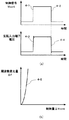
図4に示す特性は、抵抗114を小さい定数(例えば10kΩ)として、抵抗115及びダイオード116がない図13に示す従来の回路における特性である。図4(a)は制御信号Vcontとオペアンプ109の反転入力端子(−端子)の入力電圧について、それぞれ時間軸で表したグラフである。また図4(b)は、そのときの制御電圧Vcontの変化量、つまり制御量ΔVcontと、電圧制御発振器(VCO)110の出力の周波数変化量Δfの関係を表したグラフである。
The characteristic shown in FIG. 4 is a characteristic in the conventional circuit shown in FIG. 13 in which the
図4(a)のように、抵抗114の定数が小さい場合は、制御信号Vcontの立ち上り(4−1)に対して、反転入力端子電圧は急峻に立ち上がる(4−3)。また、制御信号Vcontの立ち下り(4−2)に対しても、反転入力端子電圧は急峻に立ち下がる(4−4)。周波数変化量Δfは、オペアンプ109における制御信号に応じた反転入力端子電圧の変化分と、圧電トランス出力電圧のフィードバックに応じた非反転入力端子の変化分(ここでは説明しないこととする)とによって決定するオペアンプ109の出力端子電圧、つまり電圧制御発振器(VCO)110の入力電圧の変化により決まる。
As shown in FIG. 4A, when the constant of the
したがって、急峻な立ち上り、立ち下りに対しては、図4(b)に示すように、制御量ΔVcontに対して周波数変化量Δfが急峻な傾きを持った特性を描く(4−5)。同図にて各軸の交差する部分が目標とする制御電圧或いは駆動周波数である。この場合は、共振周波数f0(図3参照)付近においても周波数変化量Δfが大きい為に、目標とする駆動周波数を通り越しさらに共振周波数f0を越えてしまう可能性がある。 Therefore, for the steep rise and fall, as shown in FIG. 4B, the frequency change Δf has a characteristic with a steep slope with respect to the control amount ΔVcont (4-5). In the figure, the intersection of each axis is the target control voltage or drive frequency. In this case, since the frequency change amount Δf is large even in the vicinity of the resonance frequency f0 (see FIG. 3), there is a possibility that the target drive frequency is passed and the resonance frequency f0 is exceeded.
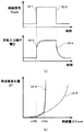
一方、図5に示す特性は、抵抗114を大きい定数(例えば100kΩ)として、抵抗115及びダイオード116がない図13に示す従来の回路における特性である。図5(a)は制御信号Vcontとオペアンプ109の反転入力端子(−端子)の入力電圧について、それぞれ時間軸で表したグラフである。また図5(b)は、そのときの制御電圧Vcontの変化量、つまり制御量ΔVcontと周波数変化量Δfの関係を表したグラフである。
On the other hand, the characteristic shown in FIG. 5 is the characteristic in the conventional circuit shown in FIG. FIG. 5A is a graph showing the control signal Vcont and the input voltage of the inverting input terminal (−terminal) of the
図5(a)のように、抵抗114の定数が大きい場合は、制御信号Vcontの立ち上り(5−1)に対して、反転入力端子電圧は緩やかに立ち上がる(5−3)。また、制御信号Vcontの立ち下り(5−2)に対しても、反転入力端子電圧は緩やかに立ち下がる(5−4)。これにより、図5(b)に示すように、制御量ΔVcontに対して周波数変化量Δfが緩やかな傾きを持った特性を描く(5−5)。このため、特に制御量ΔVcontが大きい場合は、目標とする周波数への制御時間が長くなる。
As shown in FIG. 5A, when the constant of the
他方、図6に示す特性は、抵抗114を小さい定数(例えば10kΩ)として、抵抗115を大きい定数(例えば100kΩ)として、ダイオード116を抵抗値のより高い抵抗115に対して並列に接続した、図1に示す本実施例の回路における特性である。図6(a)は制御信号Vcontとオペアンプ109の反転入力端子(−端子)の入力電圧について、それぞれ時間軸で表したグラフである。また図6(b)は、そのときの制御電圧Vcontの変化量、つまり制御量ΔVcontと、周波数変化量Δfの関係を表したグラフである。
On the other hand, the characteristics shown in FIG. 6 are obtained by connecting the
図6(a)のように、制御信号Vcontの立ち上り(6−1)に対して、反転入力端子電圧は急峻に立ち上がるものの、目標電圧付近では緩やかな特性を描く(6−3)。また、制御信号Vcontの立ち下り(6−2)に対しては、反転入力端子電圧は緩やかに立ち下がる(6−4)。これにより、立ち上りについては図6(b)に実線で示すように、制御量ΔVcontが制御量v6以上の場合は急峻な特性を描き、v6以下は緩やかな特性を描く(6−5)。 As shown in FIG. 6A, although the inverting input terminal voltage rises steeply with respect to the rising edge (6-1) of the control signal Vcont, a gentle characteristic is drawn near the target voltage (6-3). Further, the inverting input terminal voltage gently falls (6-4) with respect to the fall (6-2) of the control signal Vcont. As a result, as shown by a solid line in FIG. 6 (b), when the control amount ΔVcont is greater than or equal to the control amount v6, a steep characteristic is drawn, and when it is less than v6, a gentle characteristic is drawn (6-5).
この制御量v6について説明すると、抵抗115にアノードを制御信号入力側として並列に接続されたダイオード116の順方向特性を利用し、抵抗115の両端の電圧つまりダイオード116の両端の電圧が約0.5V以上の場合はダイオード116に電流が流れるので、積分回路としては抵抗115がバイパスされ、抵抗114の定数のみが積分回路動作に寄与するようになる。また、周波数制御が行われる過程でオペアンプ109の非反転入力端子(+端子)の電圧が上がるにつれて反転入力端子電圧も上がり、結果としてダイオード116の両端の電圧が約0.5V以下になると、ダイオード116に電流が流れなくなる為、積分回路として抵抗115が加わり、抵抗114と115を足したもので積分回路動作するようになる。
The control amount v6 will be described. The forward characteristic of the
また、立ち下りについては破線で示すように、制御量ΔVcontに対して周波数変化量Δfが概ね緩やかな傾きを持った特性を描く(6−6)。すなわち、立ち上り動作については、目標とする制御電圧との差が大きい領域では周波数変化量Δfは大きく、目標とする制御電圧との差が小さい領域では周波数変化量Δfが小さくなり、図3に示すような圧電トランスの周波数特性に応じた理想的な制御が可能となる。
本実施例では、積分回路に定数の異なる抵抗を2つ備え、ダイオードの順方向特性を用いることにより、立ち上り動作に対して簡単かつ安価な構成で制御量ΔVcontに応じた周波数変化量Δfの理想的な制御を可能とした。
なお、画像形成装置の説明を、タンデム方式のカラー画像形成装置を例に説明したが、高圧バイアスを用いた画像形成装置であれば本発明の適用範囲とする。
As for the falling, as shown by a broken line, a characteristic in which the frequency change amount Δf has a generally gentle slope with respect to the control amount ΔVcont is drawn (6-6). That is, for the rising operation, the frequency change amount Δf is large in a region where the difference from the target control voltage is large, and the frequency change amount Δf is small in a region where the difference from the target control voltage is small, as shown in FIG. Ideal control according to the frequency characteristics of such a piezoelectric transformer is possible.
In this embodiment, the integration circuit is provided with two resistors having different constants and uses the forward characteristics of the diode, so that the ideal frequency change amount Δf corresponding to the control amount ΔVcont can be obtained with a simple and inexpensive configuration for the rising operation. Control was possible.
The image forming apparatus has been described by taking a tandem color image forming apparatus as an example. However, any image forming apparatus using a high-voltage bias is within the scope of the present invention.
[実施例2]
実施例1では圧電トランス式高圧電源における制御の立ち上り特性を向上することのできる実施例を説明した。しかし、高圧出力制御においては、立ち上り特性と共に立ち下り特性も向上させる必要がある場合もある。このことを鑑みて、本実施例2では、上述の実施例1の構成にさらに部品を1つ追加することで立ち上り特性と立ち下り特性の両方を向上させることのできる圧電トランス式高圧電源について図7および図8を参照し説明する。なお、実施例1と同様の構成に関してはその説明を省略する。
[Example 2]
In the first embodiment, the embodiment that can improve the start-up characteristic of the control in the piezoelectric transformer type high voltage power source has been described. However, in high voltage output control, it may be necessary to improve the falling characteristics as well as the rising characteristics. In view of this, in the second embodiment, a piezoelectric transformer type high-voltage power supply that can improve both rising characteristics and falling characteristics by adding one more component to the configuration of the first embodiment described above is illustrated. 7 and FIG. Note that the description of the same configuration as that of the first embodiment is omitted.
図7は本実施例の圧電トランス式高圧電源の構成を示す図である。
本実施例と実施例1との主たる相違点は、抵抗114よりも抵抗値の高い抵抗115にアノード端子を制御信号入力側として並列に接続したダイオード116に加え、さらにカソード端子を制御信号入力側としてダイオード117を並列に接続したことである。
FIG. 7 is a diagram showing the configuration of the piezoelectric transformer type high-voltage power source of this embodiment.
The main difference between the present embodiment and the first embodiment is that, in addition to the
図8に示す特性は、抵抗114を小さい定数(例えば10kΩ)とし、抵抗115を大きい定数(例えば100kΩ)として、ダイオード116とダイオード117をそれぞれ逆方向にして抵抗値のより高い抵抗115に対して並列に接続した、図7に示す本実施例の回路における特性である。図8(a)は制御信号Vcontとオペアンプ109の反転入力端子(−端子)の入力電圧について、それぞれ時間軸で表したグラフである。また図8(b)は、そのときの制御電圧Vcontの変化量、つまり制御量ΔVcontと、周波数変化量Δfの関係を表したグラフである。
The characteristic shown in FIG. 8 is that the
図8(a)のように、制御信号Vcontの立ち上り(8−1)に対して、反転入力端子電圧は急峻に立ち上がるものの、目標電圧付近では緩やかな特性を描く(8−3)。また、制御信号Vcontの立ち下り(8−2)に対しても、反転入力端子電圧は急峻に立ち下がるものの、目標電圧(グラフでは0V)付近では緩やかな特性を描く(8−4)。これにより、立ち上り、立ち下りの両方について図8(b)に示すように、制御量ΔVcontが制御量v8以上の場合は急峻な特性を描き、v8以下は緩やかな特性を描く(8−5)。この制御量v8について、立ち上り時の回路動作については実施例1で説明したので、ここでは省略する。 As shown in FIG. 8A, the inverting input terminal voltage rises steeply with respect to the rising edge of the control signal Vcont (8-1), but a gentle characteristic is drawn near the target voltage (8-3). Also, the inverting input terminal voltage sharply falls with respect to the falling edge of the control signal Vcont (8-2), but a gentle characteristic is drawn near the target voltage (0 V in the graph) (8-4). Thus, as shown in FIG. 8B for both rising and falling, when the control amount ΔVcont is greater than or equal to the control amount v8, a steep characteristic is drawn, and when v8 or less, a gentle characteristic is drawn (8-5). . Regarding the control amount v8, since the circuit operation at the time of rising has been described in the first embodiment, it is omitted here.
立ち下り時においては、抵抗115にカソードを制御信号入力側として並列に接続されたダイオード117の順方向特性を利用し、抵抗115の両端の電圧つまりダイオード117の両端の電圧が約0.5V以上の場合はダイオード117に電流が流れるので、積分回路としては抵抗115が見えなくなり、抵抗114の定数のみが積分回路動作に影響するようになる。また、周波数制御が行われる過程でオペアンプ109の非反転入力端子(+端子)の電圧が下がるにつれて反転入力端子電圧も下がり、ダイオード117の両端の電圧が約0.5V以下になると、ダイオード117に電流が流れなくなる為、積分回路として抵抗115が加わり、抵抗114と115を足したものが積分回路動作に影響するようになる。なお、立ち下がり動作においては、ダイオード116は逆方向特性となるために、回路上は動作していないことになる。
At the time of falling, the forward characteristic of the
以上のように、立ち上り及び立ち下りの両方の動作において、目標とする制御電圧との差が大きい領域では周波数変化量Δfは大きく、目標とする制御電圧との差が小さい領域では周波数変化量Δfは小さくすることができる。
本実施例では、実施例1に加え、さらに逆方向に並列接続したダイオードを備え、2つのダイオードの順方向特性を用いることにより、立ち上り動作と立ち下り動作の両方に対して簡単かつ安価な構成で制御量ΔVcontに応じた周波数変化量Δfの理想的な制御を可能とした。
As described above, in both the rising and falling operations, the frequency change amount Δf is large in the region where the difference from the target control voltage is large, and the frequency change amount Δf in the region where the difference from the target control voltage is small. Can be small.
In this embodiment, in addition to the first embodiment, a diode further connected in parallel in the reverse direction is provided, and the forward characteristics of the two diodes are used, so that the configuration is simple and inexpensive for both the rising operation and the falling operation. Thus, it is possible to ideally control the frequency change amount Δf according to the control amount ΔVcont.
[実施例3]
以下、本発明の第3実施例を図面に基づいて説明する。
図9は、実施例1或いは実施例2で示した圧電トランス式高圧電源を別の回路構成により実現したものである。なお、実施例1及び実施例2と同様の構成に関してはその説明を省略する。
本実施例と実施例1或いは実施例2との主たる相違点は、抵抗114よりも抵抗値の高い抵抗115にカソード端子を制御信号入力側としてツェナーダイオード118を並列に接続したことである。
[Example 3]
Hereinafter, a third embodiment of the present invention will be described with reference to the drawings.
FIG. 9 shows the piezoelectric transformer type high voltage power source shown in the first embodiment or the second embodiment realized by another circuit configuration. Note that a description of the same configurations as those of the first and second embodiments is omitted.
The main difference between the present embodiment and the first or second embodiment is that a
図10に示す特性は、抵抗114を小さい定数(例えば10kΩ)として、抵抗115を大きい定数(例えば100kΩ)として、ツェナーダイオード118を抵抗値のより高い抵抗115に対して並列に接続した、図9に示す本実施例の回路における特性である。図10(a)は制御信号Vcontとオペアンプ109の反転入力端子(−端子)の入力電圧について、それぞれ時間軸で表したグラフである。また図10(b)は、そのときの制御電圧Vcontの変化量、つまり制御量ΔVcontと、周波数変化量Δfの関係を表したグラフである。
The characteristic shown in FIG. 10 is that the
図10(a)のように、制御信号Vcontの立ち上り(10−1)に対して、反転入力端子電圧は急峻に立ち上がるものの、目標電圧付近では緩やかな特性を描く(10−3)。また、制御信号Vcontの立ち下り(10−2)に対しても、反転入力端子電圧は急峻に立ち下がるものの、目標電圧(グラフでは0V)付近では緩やかな特性を描く(10−4)。このとき、立ち上りと立ち下りとでは緩やかな特性になるタイミングが若干異なる。 As shown in FIG. 10A, the inverting input terminal voltage rises steeply with respect to the rising edge of the control signal Vcont (10-1), but a gentle characteristic is drawn near the target voltage (10-3). Also, the inverting input terminal voltage sharply falls with respect to the falling edge of the control signal Vcont (10-2), but a gentle characteristic is drawn near the target voltage (0 V in the graph) (10-4). At this time, the timing at which the characteristics become gentle differs slightly between the rising edge and the falling edge.
立ち上りについては、図10(b)に実線で示すように、制御量ΔVcontが制御量v10a以上の場合は急峻な特性を描き、v10a以下は緩やかな特性を描く(10−5)。また、立ち下りについては、破線で示すように、制御量ΔVcontが制御量v10b以上の場合は急峻な特性を描き、v10b以下は緩やかな特性を描く(10−6)。
上述した制御量v10aについては、抵抗115にカソードを制御信号入力側として並列に接続されたツェナーダイオード118のツェナー電圧を利用し、抵抗115の両端の電圧つまりツェナーダイオード118の両端の電圧がツェナー電圧以上の場合は逆方向に電流が流れるので、積分回路としては抵抗115が見えなくなり、抵抗114の定数のみが積分回路動作に影響するようになる。
As for the rise, as shown by a solid line in FIG. 10B, when the control amount ΔVcont is equal to or greater than the control amount v10a, a steep characteristic is drawn, and when v10a or less, a gentle characteristic is drawn (10-5). As for the falling, as shown by a broken line, when the control amount ΔVcont is equal to or greater than the control amount v10b, a steep characteristic is drawn, and when v10b or less, a gentle characteristic is drawn (10-6).
For the control amount v10a described above, the Zener voltage of the
また、上述した制御量v10bについては、抵抗115に並列に接続されたツェナーダイオード118の順方向特性を利用し、ツェナーダイオード118の両端の電圧が約0.5V以上の場合は順方向の電流が流れるので、積分回路としては抵抗115が見えなくなり、抵抗114の定数のみが積分回路動作に影響するようになる。また、周波数制御が行われる過程でオペアンプ109の非反転入力端子(+端子)の電圧が下がるにつれて反転入力端子電圧も下がり、ツェナーダイオード118の両端の電圧が約0.5V以下になると、ツェナーダイオード118に電流が流れなくなる為、積分回路として抵抗115が加わり、抵抗114と115を足したものが積分回路動作に影響するようになる。
For the control amount v10b described above, the forward characteristic of the
以上のように、ツェナーダイオードを1つ用いることにより、立ち上りと立ち下りの両方の動作において、目標とする制御電圧との差が大きい領域では周波数変化量Δfを大きく、目標とする制御電圧との差が小さい領域では周波数変化量Δfを小さくすることができる。したがって、目的とする立ち上り特性に合うツェナー電圧のツェナーダイオードを用いることにより、自由に設計することができる。 As described above, by using one Zener diode, in both rising and falling operations, the frequency change amount Δf is increased in a region where the difference from the target control voltage is large, In a region where the difference is small, the frequency change amount Δf can be reduced. Therefore, it is possible to design freely by using a Zener diode having a Zener voltage suitable for the desired rise characteristic.
なお、本実施例ではツェナーダイオードのカソードを制御信号入力側として抵抗に並列に接続したが、アノードを制御信号入力側にしても同様に設計可能である。
以上からわかるように、本実施例では、前述の実施例2よりも簡単な構成により、動作と立ち下り動作の両方に対して簡単かつ安価な構成で制御量ΔVcontに応じた周波数変化量Δfの理想的な制御を可能とした。
In the present embodiment, the cathode of the Zener diode is connected in parallel to the resistor as the control signal input side, but the design can be similarly made even when the anode is the control signal input side.
As can be seen from the above, in the present embodiment, the frequency change amount Δf corresponding to the control amount ΔVcont is configured with a simpler and cheaper configuration for both the operation and the falling operation with a simpler configuration than the above-described second embodiment. Ideal control is possible.
[実施例4]
以下、本発明の第4実施例を図面に基づいて説明する。
図11は、実施例1で示した圧電トランス式高圧電源をさらに発展させたものである。なお、これまで説明してきた実施例と同様の構成に関してはその説明を省略する。
[Example 4]
The fourth embodiment of the present invention will be described below with reference to the drawings.
FIG. 11 shows a further development of the piezoelectric transformer type high voltage power source shown in the first embodiment. Note that a description of the same configuration as that of the embodiment described so far is omitted.
本実施例と実施例1との主たる相違点は、抵抗119を抵抗114、115対して直列に接続し、さらに抵抗119に対してアノード端子を制御信号入力側としてダイオード117を並列に接続したことである。また、抵抗114、115、119の各抵抗値R114、R115、R119の関係は、R119>R115>R114としたことである。
The main difference between the present embodiment and the first embodiment is that a
図12に示す特性は、抵抗114を小さい定数(例えば10kΩ)として、抵抗115を次に大きい定数(例えば100kΩ)として、抵抗119を最も大きい定数(例えば200kΩ)とした図11の回路における特性である。図12(a)は制御信号Vcontとオペアンプ109の反転入力端子(−端子)の入力電圧について、それぞれ時間軸で表したグラフである。また図12(b)は、そのときの制御電圧Vcontの変化量、つまり制御量ΔVcontと、周波数変化量Δfの関係を表したグラフである。
The characteristics shown in FIG. 12 are the characteristics in the circuit of FIG. 11 in which the
図12(a)のように、制御信号Vcontの立ち上り(12−1)に対して、反転入力端子電圧は急峻に立ち上がるものの、目標電圧付近では緩やかな特性を描く(12−3)。このとき、(12−3)で表される特性曲線は、3段階の傾き変化をもつ。また、制御信号Vcontの立ち下り(12−2)に対しては、反転入力端子電圧は緩やかに立ち下がる(12−4)。これにより、立ち上りについては図6(b)に実線で示すように、制御量ΔVcontが制御量v12a以上の場合、制御量v12b以上v12a以下の場合、制御量v12b以下の場合で異なる特性を描く(12−5)。 As shown in FIG. 12A, although the inverting input terminal voltage rises steeply with respect to the rise of the control signal Vcont (12-1), it shows a gentle characteristic near the target voltage (12-3). At this time, the characteristic curve represented by (12-3) has a three-step gradient change. Further, the inverting input terminal voltage gently falls (12-4) with respect to the fall (12-2) of the control signal Vcont. As a result, as shown by a solid line in FIG. 6B, the characteristics of the rise are different depending on whether the control amount ΔVcont is the control amount v12a or more, the control amount v12b or more and v12a or less, or the control amount v12b or less ( 12-5).
この制御量v12a及びv12bについて説明すると、抵抗115と抵抗119にそれぞれアノードを制御信号入力側として並列に接続されたダイオード116とダイオード117の順方向特性を利用し、抵抗115、119の両端の電圧つまりダイオード116、117の両端の電圧が約0.5V以上の場合はダイオードに電流が流れるので、積分回路としては抵抗115、119がバイパスされ、抵抗114の定数のみが積分回路動作に寄与するようになる。
The control amounts v12a and v12b will be described. Using the forward characteristics of the
制御信号Vcontの電圧が上昇して周波数制御が行われる過程において、オペアンプ109の非反転入力端子(+端子)の電圧が上がるにつれて反転入力端子電圧も上がり、抵抗115に並列に接続されたダイオード116の両端の電圧が約0.5V以下になると、ダイオード116に電流が流れなくなる為、積分回路として抵抗115が加わり、抵抗114と抵抗115を足したもので積分回路動作するようになる。これが制御量v12aにおける回路動作である。続いて、抵抗115より抵抗値の大きい抵抗119に並列に接続されたダイオード117の両端の電圧が約0.5V以下になると、ダイオード117に電流が流れなくなる為、積分回路として抵抗119も加わり、抵抗114と抵抗115、さらに抵抗119を足したもので積分回路動作するようになる。これが制御量v12bにおける回路動作である。
In the process in which frequency control is performed by increasing the voltage of the control signal Vcont, the voltage of the inverting input terminal increases as the voltage of the non-inverting input terminal (+ terminal) of the
以上のように、制御信号の立ち上り動作において目標とする制御電圧との差が小さくなるにつれて周波数変化量Δfの変化量を段階的に変化させることが可能となるので、実施例1で示した回路構成よりもさらに精度の高い周波数制御を実現できる。ここでは3段階の制御が可能な回路構成を示した。抵抗及びそれに並列に接続したダイオードを制御信号に対して直列に組み合わせることによって、簡単に段数を増やしてより精度の高い制御を実現できる。 As described above, since the change amount of the frequency change amount Δf can be changed stepwise as the difference from the target control voltage in the rising operation of the control signal becomes smaller, the circuit shown in the first embodiment. It is possible to realize frequency control with higher accuracy than the configuration. Here, a circuit configuration capable of three-stage control is shown. By combining a resistor and a diode connected in parallel with the resistor in series with the control signal, it is possible to easily increase the number of stages and realize more accurate control.
101…圧電トランス
102,103,116…ダイオード
104…高圧コンデンサ
105,106,107,114,115…抵抗
108…保護用抵抗
109…オペアンプ
110…電圧制御発振器(VCO)
111…トランジスタ
112…インダクタ
113…コンデンサ
201…DCコントローラ
202…高圧電源(圧電トランス式高圧電源装置)
401…カラーレーザプリンタ(画像形成装置)
DESCRIPTION OF
111 ...
401: Color laser printer (image forming apparatus)
Claims (11)
圧電トランスと、前記圧電トランスを駆動する駆動手段と、前記圧電トランスから出力される出力電圧を設定する制御信号を出力する電圧設定手段と、前記圧電トランスからの出力電圧を検出する検出手段と、前記検出手段で検出された電圧が前記電圧設定手段からの前記制御信号に応じて、前記駆動手段に出力する周波数信号の周波数を制御する出力制御手段と、を有する高圧電源を備え、
前記電圧設定手段からの前記出力制御手段への前記制御信号の入力部に、第1抵抗と、前記第1抵抗と直列に接続され、前記第1抵抗の抵抗値よりも抵抗値が小さい第2抵抗と、前記第1抵抗と並列に接続した整流素子とを備え、
前記電圧設定手段からの前記制御信号による制御電圧値が所定値以上の場合は、前記第1抵抗を介して前記制御信号が前記出力制御手段に入力され、前記制御信号による前記制御電圧値が前記所定値未満の場合は、前記第1抵抗及び前記第2抵抗を介して前記制御信号が前記出力制御手段に入力される
ことを特徴とする画像形成装置。 A latent image forming unit that forms an electrostatic latent image on an image carrier, a developing unit that supplies toner to the electrostatic latent image to form a toner image, and a transfer unit that transfers the toner image to a transfer material; In an image forming apparatus comprising fixing means for fixing a toner image transferred to a transfer material to the transfer material,
A piezoelectric transformer; drive means for driving the piezoelectric transformer; voltage setting means for outputting a control signal for setting an output voltage output from the piezoelectric transformer; and detection means for detecting an output voltage from the piezoelectric transformer; An output control means for controlling the frequency of the frequency signal output to the drive means in accordance with the control signal from the voltage setting means, the voltage detected by the detection means, and a high-voltage power supply having
A first resistor and a second resistor having a resistance value smaller than the resistance value of the first resistor are connected in series with the first resistor to the input portion of the control signal from the voltage setting means to the output control means. A resistor and a rectifying element connected in parallel with the first resistor;
When the control voltage value by the control signal from the voltage setting means is greater than or equal to a predetermined value, the control signal is input to the output control means through the first resistor, and the control voltage value by the control signal is When the value is less than a predetermined value, the control signal is input to the output control unit via the first resistor and the second resistor.
前記ダイオードのアノードを前記制御信号の入力側に接続したことを特徴とする請求項1または請求項2に記載の画像形成装置。 The rectifying element is a diode,
The image forming apparatus according to claim 1, wherein an anode of the diode is connected to an input side of the control signal.
圧電トランスと、
前記圧電トランスを駆動する駆動手段と、
前記圧電トランスの出力電圧を設定するための制御信号を出力する電圧設定手段と、
前記圧電トランスからの出力電圧を検出する検出手段と、
前記検出手段で検出された電圧が前記電圧設定手段からの前記制御信号に応じて、前記駆動手段に出力する周波数信号の周波数を制御する出力制御手段と、備え、
前記電圧設定手段からの前記出力制御手段への前記制御信号の入力部に、第1抵抗と、前記第1抵抗と直列に接続され、前記第1抵抗の抵抗値よりも抵抗値が小さい第2抵抗と、前記第1抵抗と並列に接続した整流素子とを備え、
前記電圧設定手段からの前記制御信号による制御電圧値が所定値以上の場合は、前記第1抵抗を介して前記制御信号が前記出力制御手段に入力され、前記制御信号による前記制御電圧値が前記所定値未満の場合は、前記第1抵抗及び前記第2抵抗を介して前記制御信号が前記出力制御手段に入力される
ことを特徴とする高圧電源装置。 In a high voltage power supply device used in an image forming apparatus and supplying a voltage to the image forming apparatus ,
A piezoelectric transformer,
Driving means for driving the piezoelectric transformer;
Voltage setting means for outputting a control signal for setting the output voltage of the piezoelectric transformer;
Detecting means for detecting an output voltage from the piezoelectric transformer;
An output control means for controlling a frequency of a frequency signal output to the driving means in accordance with the control signal from the voltage setting means, the voltage detected by the detection means;
A first resistor and a second resistor having a resistance value smaller than the resistance value of the first resistor are connected in series with the first resistor to the input portion of the control signal from the voltage setting means to the output control means. A resistor and a rectifying element connected in parallel with the first resistor;
When the control voltage value by the control signal from the voltage setting means is greater than or equal to a predetermined value, the control signal is input to the output control means through the first resistor, and the control voltage value by the control signal is When the voltage is less than a predetermined value, the control signal is input to the output control means via the first resistor and the second resistor.
前記ダイオードのアノードを前記制御信号の入力側に接続したことを特徴とする請求項7に記載の高圧電源装置。 The rectifying element is a diode,
The high-voltage power supply device according to claim 7, wherein an anode of the diode is connected to an input side of the control signal.
Priority Applications (1)
| Application Number | Priority Date | Filing Date | Title |
|---|---|---|---|
| JP2004280299A JP4763990B2 (en) | 2004-09-27 | 2004-09-27 | Image forming apparatus and high-voltage power supply device used for image forming apparatus |
Applications Claiming Priority (1)
| Application Number | Priority Date | Filing Date | Title |
|---|---|---|---|
| JP2004280299A JP4763990B2 (en) | 2004-09-27 | 2004-09-27 | Image forming apparatus and high-voltage power supply device used for image forming apparatus |
Publications (3)
| Publication Number | Publication Date |
|---|---|
| JP2006091757A JP2006091757A (en) | 2006-04-06 |
| JP2006091757A5 JP2006091757A5 (en) | 2009-12-03 |
| JP4763990B2 true JP4763990B2 (en) | 2011-08-31 |
Family
ID=36232777
Family Applications (1)
| Application Number | Title | Priority Date | Filing Date |
|---|---|---|---|
| JP2004280299A Expired - Fee Related JP4763990B2 (en) | 2004-09-27 | 2004-09-27 | Image forming apparatus and high-voltage power supply device used for image forming apparatus |
Country Status (1)
| Country | Link |
|---|---|
| JP (1) | JP4763990B2 (en) |
Families Citing this family (12)
| Publication number | Priority date | Publication date | Assignee | Title |
|---|---|---|---|---|
| JP5241207B2 (en) * | 2006-12-13 | 2013-07-17 | キヤノン株式会社 | Power supply device and image forming apparatus |
| JP5121538B2 (en) * | 2008-04-02 | 2013-01-16 | キヤノン株式会社 | Image forming apparatus |
| JP5394041B2 (en) * | 2008-10-29 | 2014-01-22 | 株式会社沖データ | Power supply device and image forming apparatus |
| JP5198239B2 (en) * | 2008-12-22 | 2013-05-15 | 株式会社沖データ | Power supply device and image forming apparatus |
| US8265511B2 (en) | 2008-10-29 | 2012-09-11 | Oki Data Corporation | Power source device and image forming apparatus |
| JP5380085B2 (en) | 2009-01-28 | 2014-01-08 | 株式会社沖データ | Piezoelectric transformer driving device, cold cathode tube inverter, cold cathode tube driving device, and image forming apparatus |
| JP5247513B2 (en) | 2009-02-12 | 2013-07-24 | 株式会社沖データ | Power supply device and image forming apparatus |
| JP5394164B2 (en) * | 2009-08-18 | 2014-01-22 | 株式会社沖データ | Power supply device and image forming apparatus |
| JP4902708B2 (en) | 2009-08-27 | 2012-03-21 | 株式会社沖データ | Power supply device and image forming apparatus |
| JP5394195B2 (en) * | 2009-10-28 | 2014-01-22 | 株式会社沖データ | Power supply device and image forming apparatus |
| JP5882574B2 (en) | 2009-12-10 | 2016-03-09 | キヤノン株式会社 | High voltage power supply device and image forming apparatus having the same |
| JP5303633B2 (en) * | 2011-12-27 | 2013-10-02 | 株式会社沖データ | Power supply control device and power supply control method |
Family Cites Families (2)
| Publication number | Priority date | Publication date | Assignee | Title |
|---|---|---|---|---|
| JPH0957618A (en) * | 1995-08-18 | 1997-03-04 | Tokyo Seimitsu Co Ltd | Fixed dimension processing device |
| JPH11206113A (en) * | 1997-12-29 | 1999-07-30 | Canon Inc | High-voltage power unit |
-
2004
- 2004-09-27 JP JP2004280299A patent/JP4763990B2/en not_active Expired - Fee Related
Also Published As
| Publication number | Publication date |
|---|---|
| JP2006091757A (en) | 2006-04-06 |
Similar Documents
| Publication | Publication Date | Title |
|---|---|---|
| JP5247908B2 (en) | Power supply, control circuit, power supply for image forming device | |
| EP1750179B1 (en) | Image forming apparatus and power supply | |
| JP4332528B2 (en) | Power supply device and image forming apparatus having power supply device | |
| JP4763990B2 (en) | Image forming apparatus and high-voltage power supply device used for image forming apparatus | |
| US7196475B2 (en) | Image forming apparatus utilizing a piezoelectric-transformer high-voltage power supply and method for controlling the same | |
| JP4420458B2 (en) | High voltage power supply, image forming device | |
| US7579749B2 (en) | Power supply device and image forming apparatus using the power supply device | |
| JP2007043891A (en) | Power supply device and image forming device using same | |
| JP2008224861A (en) | Image forming apparatus and piezoelectric transformer system high voltage power unit | |
| JP6448305B2 (en) | Power supply device and image forming apparatus | |
| JP4944632B2 (en) | Circuit board, high voltage power supply device and image forming apparatus | |
| JP4981323B2 (en) | Power supply for image forming device | |
| JP5188022B2 (en) | Image forming apparatus | |
| JP2008099372A (en) | Image forming apparatus and piezoelectric transformer type high-voltage power supply apparatus | |
| JP2006204016A (en) | High-voltage power supply unit and image forming apparatus | |
| JP4838581B2 (en) | Image forming apparatus | |
| JP2004077692A (en) | Image forming apparatus | |
| JP2006201351A (en) | Image forming apparatus | |
| US11835910B2 (en) | Power source apparatus and image forming apparatus having a control unit configured to switch a target voltage of an output voltage output from a secondary side of a transformer | |
| JP2009153293A (en) | Piezoelectric transformer high-voltage power supply circuit | |
| JP2007011087A (en) | Power supply device and image forming apparatus | |
| JP2007101948A (en) | Image forming apparatus | |
| KR100790677B1 (en) | Image forming apparatus and power supply | |
| JP5335272B2 (en) | High voltage power supply device and image forming apparatus using the same | |
| JP2008301692A (en) | Power supply unit and image forming apparatus |
Legal Events
| Date | Code | Title | Description |
|---|---|---|---|
| A621 | Written request for application examination |
Free format text: JAPANESE INTERMEDIATE CODE: A621 Effective date: 20070911 |
|
| A521 | Written amendment |
Free format text: JAPANESE INTERMEDIATE CODE: A523 Effective date: 20091021 |
|
| A977 | Report on retrieval |
Free format text: JAPANESE INTERMEDIATE CODE: A971007 Effective date: 20100402 |
|
| A131 | Notification of reasons for refusal |
Free format text: JAPANESE INTERMEDIATE CODE: A131 Effective date: 20100723 |
|
| A521 | Written amendment |
Free format text: JAPANESE INTERMEDIATE CODE: A523 Effective date: 20100921 |
|
| RD02 | Notification of acceptance of power of attorney |
Free format text: JAPANESE INTERMEDIATE CODE: A7422 Effective date: 20101106 |
|
| A131 | Notification of reasons for refusal |
Free format text: JAPANESE INTERMEDIATE CODE: A131 Effective date: 20110318 |
|
| A521 | Written amendment |
Free format text: JAPANESE INTERMEDIATE CODE: A523 Effective date: 20110513 |
|
| TRDD | Decision of grant or rejection written | ||
| A01 | Written decision to grant a patent or to grant a registration (utility model) |
Free format text: JAPANESE INTERMEDIATE CODE: A01 Effective date: 20110603 |
|
| A01 | Written decision to grant a patent or to grant a registration (utility model) |
Free format text: JAPANESE INTERMEDIATE CODE: A01 |
|
| A61 | First payment of annual fees (during grant procedure) |
Free format text: JAPANESE INTERMEDIATE CODE: A61 Effective date: 20110610 |
|
| FPAY | Renewal fee payment (event date is renewal date of database) |
Free format text: PAYMENT UNTIL: 20140617 Year of fee payment: 3 |
|
| R150 | Certificate of patent or registration of utility model |
Free format text: JAPANESE INTERMEDIATE CODE: R150 |
|
| LAPS | Cancellation because of no payment of annual fees |