JP5378552B2 - Amorphous carbon film, method for forming amorphous carbon film, conductive member provided with amorphous carbon film, and separator for fuel cell - Google Patents
Amorphous carbon film, method for forming amorphous carbon film, conductive member provided with amorphous carbon film, and separator for fuel cell Download PDFInfo
- Publication number
- JP5378552B2 JP5378552B2 JP2012016256A JP2012016256A JP5378552B2 JP 5378552 B2 JP5378552 B2 JP 5378552B2 JP 2012016256 A JP2012016256 A JP 2012016256A JP 2012016256 A JP2012016256 A JP 2012016256A JP 5378552 B2 JP5378552 B2 JP 5378552B2
- Authority
- JP
- Japan
- Prior art keywords
- amorphous carbon
- carbon film
- gas
- film
- less
- Prior art date
- Legal status (The legal status is an assumption and is not a legal conclusion. Google has not performed a legal analysis and makes no representation as to the accuracy of the status listed.)
- Expired - Fee Related
Links
Images


Classifications
-
- H—ELECTRICITY
- H01—ELECTRIC ELEMENTS
- H01M—PROCESSES OR MEANS, e.g. BATTERIES, FOR THE DIRECT CONVERSION OF CHEMICAL ENERGY INTO ELECTRICAL ENERGY
- H01M8/00—Fuel cells; Manufacture thereof
- H01M8/02—Details
- H01M8/0202—Collectors; Separators, e.g. bipolar separators; Interconnectors
- H01M8/0204—Non-porous and characterised by the material
- H01M8/0223—Composites
- H01M8/0228—Composites in the form of layered or coated products
-
- C—CHEMISTRY; METALLURGY
- C01—INORGANIC CHEMISTRY
- C01B—NON-METALLIC ELEMENTS; COMPOUNDS THEREOF; METALLOIDS OR COMPOUNDS THEREOF NOT COVERED BY SUBCLASS C01C
- C01B32/00—Carbon; Compounds thereof
- C01B32/05—Preparation or purification of carbon not covered by groups C01B32/15, C01B32/20, C01B32/25, C01B32/30
-
- C—CHEMISTRY; METALLURGY
- C23—COATING METALLIC MATERIAL; COATING MATERIAL WITH METALLIC MATERIAL; CHEMICAL SURFACE TREATMENT; DIFFUSION TREATMENT OF METALLIC MATERIAL; COATING BY VACUUM EVAPORATION, BY SPUTTERING, BY ION IMPLANTATION OR BY CHEMICAL VAPOUR DEPOSITION, IN GENERAL; INHIBITING CORROSION OF METALLIC MATERIAL OR INCRUSTATION IN GENERAL
- C23C—COATING METALLIC MATERIAL; COATING MATERIAL WITH METALLIC MATERIAL; SURFACE TREATMENT OF METALLIC MATERIAL BY DIFFUSION INTO THE SURFACE, BY CHEMICAL CONVERSION OR SUBSTITUTION; COATING BY VACUUM EVAPORATION, BY SPUTTERING, BY ION IMPLANTATION OR BY CHEMICAL VAPOUR DEPOSITION, IN GENERAL
- C23C16/00—Chemical coating by decomposition of gaseous compounds, without leaving reaction products of surface material in the coating, i.e. chemical vapour deposition [CVD] processes
- C23C16/22—Chemical coating by decomposition of gaseous compounds, without leaving reaction products of surface material in the coating, i.e. chemical vapour deposition [CVD] processes characterised by the deposition of inorganic material, other than metallic material
- C23C16/26—Deposition of carbon only
-
- C—CHEMISTRY; METALLURGY
- C23—COATING METALLIC MATERIAL; COATING MATERIAL WITH METALLIC MATERIAL; CHEMICAL SURFACE TREATMENT; DIFFUSION TREATMENT OF METALLIC MATERIAL; COATING BY VACUUM EVAPORATION, BY SPUTTERING, BY ION IMPLANTATION OR BY CHEMICAL VAPOUR DEPOSITION, IN GENERAL; INHIBITING CORROSION OF METALLIC MATERIAL OR INCRUSTATION IN GENERAL
- C23C—COATING METALLIC MATERIAL; COATING MATERIAL WITH METALLIC MATERIAL; SURFACE TREATMENT OF METALLIC MATERIAL BY DIFFUSION INTO THE SURFACE, BY CHEMICAL CONVERSION OR SUBSTITUTION; COATING BY VACUUM EVAPORATION, BY SPUTTERING, BY ION IMPLANTATION OR BY CHEMICAL VAPOUR DEPOSITION, IN GENERAL
- C23C16/00—Chemical coating by decomposition of gaseous compounds, without leaving reaction products of surface material in the coating, i.e. chemical vapour deposition [CVD] processes
- C23C16/44—Chemical coating by decomposition of gaseous compounds, without leaving reaction products of surface material in the coating, i.e. chemical vapour deposition [CVD] processes characterised by the method of coating
- C23C16/455—Chemical coating by decomposition of gaseous compounds, without leaving reaction products of surface material in the coating, i.e. chemical vapour deposition [CVD] processes characterised by the method of coating characterised by the method used for introducing gases into reaction chamber or for modifying gas flows in reaction chamber
- C23C16/45523—Pulsed gas flow or change of composition over time
-
- C—CHEMISTRY; METALLURGY
- C23—COATING METALLIC MATERIAL; COATING MATERIAL WITH METALLIC MATERIAL; CHEMICAL SURFACE TREATMENT; DIFFUSION TREATMENT OF METALLIC MATERIAL; COATING BY VACUUM EVAPORATION, BY SPUTTERING, BY ION IMPLANTATION OR BY CHEMICAL VAPOUR DEPOSITION, IN GENERAL; INHIBITING CORROSION OF METALLIC MATERIAL OR INCRUSTATION IN GENERAL
- C23C—COATING METALLIC MATERIAL; COATING MATERIAL WITH METALLIC MATERIAL; SURFACE TREATMENT OF METALLIC MATERIAL BY DIFFUSION INTO THE SURFACE, BY CHEMICAL CONVERSION OR SUBSTITUTION; COATING BY VACUUM EVAPORATION, BY SPUTTERING, BY ION IMPLANTATION OR BY CHEMICAL VAPOUR DEPOSITION, IN GENERAL
- C23C16/00—Chemical coating by decomposition of gaseous compounds, without leaving reaction products of surface material in the coating, i.e. chemical vapour deposition [CVD] processes
- C23C16/44—Chemical coating by decomposition of gaseous compounds, without leaving reaction products of surface material in the coating, i.e. chemical vapour deposition [CVD] processes characterised by the method of coating
- C23C16/50—Chemical coating by decomposition of gaseous compounds, without leaving reaction products of surface material in the coating, i.e. chemical vapour deposition [CVD] processes characterised by the method of coating using electric discharges
-
- H—ELECTRICITY
- H01—ELECTRIC ELEMENTS
- H01M—PROCESSES OR MEANS, e.g. BATTERIES, FOR THE DIRECT CONVERSION OF CHEMICAL ENERGY INTO ELECTRICAL ENERGY
- H01M8/00—Fuel cells; Manufacture thereof
- H01M8/02—Details
- H01M8/0202—Collectors; Separators, e.g. bipolar separators; Interconnectors
- H01M8/0204—Non-porous and characterised by the material
- H01M8/0206—Metals or alloys
-
- H—ELECTRICITY
- H01—ELECTRIC ELEMENTS
- H01M—PROCESSES OR MEANS, e.g. BATTERIES, FOR THE DIRECT CONVERSION OF CHEMICAL ENERGY INTO ELECTRICAL ENERGY
- H01M8/00—Fuel cells; Manufacture thereof
- H01M8/02—Details
- H01M8/0202—Collectors; Separators, e.g. bipolar separators; Interconnectors
- H01M8/0204—Non-porous and characterised by the material
- H01M8/0213—Gas-impermeable carbon-containing materials
-
- H—ELECTRICITY
- H01—ELECTRIC ELEMENTS
- H01M—PROCESSES OR MEANS, e.g. BATTERIES, FOR THE DIRECT CONVERSION OF CHEMICAL ENERGY INTO ELECTRICAL ENERGY
- H01M8/00—Fuel cells; Manufacture thereof
- H01M8/10—Fuel cells with solid electrolytes
- H01M2008/1095—Fuel cells with polymeric electrolytes
-
- Y—GENERAL TAGGING OF NEW TECHNOLOGICAL DEVELOPMENTS; GENERAL TAGGING OF CROSS-SECTIONAL TECHNOLOGIES SPANNING OVER SEVERAL SECTIONS OF THE IPC; TECHNICAL SUBJECTS COVERED BY FORMER USPC CROSS-REFERENCE ART COLLECTIONS [XRACs] AND DIGESTS
- Y02—TECHNOLOGIES OR APPLICATIONS FOR MITIGATION OR ADAPTATION AGAINST CLIMATE CHANGE
- Y02E—REDUCTION OF GREENHOUSE GAS [GHG] EMISSIONS, RELATED TO ENERGY GENERATION, TRANSMISSION OR DISTRIBUTION
- Y02E60/00—Enabling technologies; Technologies with a potential or indirect contribution to GHG emissions mitigation
- Y02E60/30—Hydrogen technology
- Y02E60/50—Fuel cells
-
- Y—GENERAL TAGGING OF NEW TECHNOLOGICAL DEVELOPMENTS; GENERAL TAGGING OF CROSS-SECTIONAL TECHNOLOGIES SPANNING OVER SEVERAL SECTIONS OF THE IPC; TECHNICAL SUBJECTS COVERED BY FORMER USPC CROSS-REFERENCE ART COLLECTIONS [XRACs] AND DIGESTS
- Y02—TECHNOLOGIES OR APPLICATIONS FOR MITIGATION OR ADAPTATION AGAINST CLIMATE CHANGE
- Y02P—CLIMATE CHANGE MITIGATION TECHNOLOGIES IN THE PRODUCTION OR PROCESSING OF GOODS
- Y02P70/00—Climate change mitigation technologies in the production process for final industrial or consumer products
- Y02P70/50—Manufacturing or production processes characterised by the final manufactured product
Landscapes
- Chemical & Material Sciences (AREA)
- Engineering & Computer Science (AREA)
- General Chemical & Material Sciences (AREA)
- Chemical Kinetics & Catalysis (AREA)
- Organic Chemistry (AREA)
- Life Sciences & Earth Sciences (AREA)
- Sustainable Development (AREA)
- Electrochemistry (AREA)
- Manufacturing & Machinery (AREA)
- Sustainable Energy (AREA)
- Materials Engineering (AREA)
- Mechanical Engineering (AREA)
- Metallurgy (AREA)
- Inorganic Chemistry (AREA)
- Physics & Mathematics (AREA)
- Plasma & Fusion (AREA)
- Composite Materials (AREA)
- Fuel Cell (AREA)
- Carbon And Carbon Compounds (AREA)
- Chemical Vapour Deposition (AREA)
Abstract
Description
本発明は、炭素を主成分とし導電性を示す非晶質炭素膜およびその形成方法、ならびに、燃料電池のセパレータに代表されるような非晶質炭素膜を備えた導電性部材に関する。 The present invention relates to an amorphous carbon film having carbon as a main component and showing conductivity, a method for forming the same, and a conductive member provided with an amorphous carbon film as typified by a separator for a fuel cell.
炭素は、埋設量がほぼ無限であり、かつ無害であることから資源問題および環境問題の面からも極めて優れた材料である。炭素材料は、原子間の結合形態が多様で、ダイヤモンド、ダイヤモンドライクカーボン、グラファイト、フラーレン、カーボンナノチューブといった様々な結晶構造が知られている。中でも、非晶質構造を有するダイヤモンドライクカーボン(非晶質炭素)は、高い機械強度と優れた化学安定性を有することから、各産業分野への応用が期待されている。 Carbon is an extremely excellent material from the viewpoint of resource problems and environmental problems because the amount of burying is almost infinite and harmless. Carbon materials have various bond forms between atoms, and various crystal structures such as diamond, diamond-like carbon, graphite, fullerene, and carbon nanotube are known. Among them, diamond-like carbon (amorphous carbon) having an amorphous structure is expected to be applied to various industrial fields because it has high mechanical strength and excellent chemical stability.
しかし、一般的な非晶質炭素膜の電気抵抗は、半導体から絶縁体の領域にある。非晶質炭素のさらなる用途拡大のために、非晶質炭素への導電性の付与が求められている。非晶質炭素の用途の一つとして、燃料電池のセパレータが挙げられる。図5に、単セルの固体高分子型燃料電池の一例を模式的に示す。図5の左図は、積層する前のそれぞれの構成要素の配列を示し、図5の右図は、それらを積層した状態を示す。単電池1は、電解質膜1aとそれを両側から挟持する一組の電極(空気極1bおよび燃料極1c)とから構成される。セパレータ2は、複数本の凹条が形成された凹条形成面2b、2cを有する。セパレータ2は、樹脂製のセパレータ枠3に収められ、空気極1bと凹条形成面2b、燃料極1cと凹条形成面2c、がそれぞれ対向するように積層される。こうして、電極とセパレータとの間に、電極表面と凹条とで区画されたガス流路が構成され、燃料電池における反応ガスである燃料ガスおよび酸素ガスが効率よく電極表面に供給される。
However, the electrical resistance of a general amorphous carbon film is in the region from semiconductor to insulator. In order to further expand the use of amorphous carbon, it is required to impart conductivity to amorphous carbon. One application of amorphous carbon is a fuel cell separator. FIG. 5 schematically shows an example of a single-cell solid polymer fuel cell. The left figure of FIG. 5 shows the arrangement of the respective components before lamination, and the right figure of FIG. 5 shows a state in which they are laminated. The unit cell 1 includes an
燃料電池では、燃料ガスと酸素ガスとが、互いに混合しないように分離したまま電極表面全体に供給される必要がある。したがって、セパレータには、ガスに対する気密性が必要である。さらに、セパレータには、反応により発生した電子を集電するとともに、複数のセルを積層させたときに隣接する単電池同士の電気的コネクターとして良好な導電性が必要とされる。また、電解質表面は強酸性を示すため、セパレータには、耐食性が要求される。 In a fuel cell, fuel gas and oxygen gas need to be supplied to the entire electrode surface while being separated so as not to mix with each other. Therefore, the separator needs to be gas tight. Further, the separator is required to collect electrons generated by the reaction and have good conductivity as an electrical connector between adjacent unit cells when a plurality of cells are stacked. Moreover, since the electrolyte surface is strongly acidic, the separator is required to have corrosion resistance.
そのため、セパレータの材料としては、グラファイト板材が用いられるのが一般的である。ところが、グラファイト板材は割れやすいため、グラファイト板材に複数のガス流路を形成したりその表面を平坦にしたりなどしてセパレータを生産する場合、加工性に問題がある。一方、金属材料は、導電性とともに加工性にも優れ、特に、チタンやステンレス鋼は耐食性に優れるため、セパレータの材料として使用可能である。しかしながら、耐食性に優れる金属材料は不働態化しやすいため、燃料電池の内部抵抗が増大して電圧降下を引き起こすという問題がある。そこで、金属製の基材の表面に、導電性をもつ非晶質炭素膜を被覆したセパレータが注目されつつある。 Therefore, a graphite plate is generally used as the separator material. However, since the graphite plate is easily broken, there is a problem in workability when a separator is produced by forming a plurality of gas flow paths in the graphite plate or flattening the surface thereof. On the other hand, metal materials are excellent in workability as well as conductivity, and in particular, titanium and stainless steel are excellent in corrosion resistance, and therefore can be used as separator materials. However, since the metal material having excellent corrosion resistance is easily passivated, there is a problem that the internal resistance of the fuel cell is increased to cause a voltage drop. Thus, a separator in which the surface of a metal substrate is coated with a conductive amorphous carbon film is attracting attention.
非晶質炭素に導電性を付与する方法として、非晶質炭素に金属を添加する方法が挙げられる(特許文献1および特許文献2参照)。しかしながら、添加した金属が腐食の原因となったり、他の金属と接触して用いられると凝着の原因となったり、などして非晶質炭素が本来有する化学的安定性が損なわれる場合がある。 Examples of a method for imparting conductivity to amorphous carbon include a method of adding a metal to amorphous carbon (see Patent Document 1 and Patent Document 2). However, the chemical stability inherent to amorphous carbon may be impaired due to the added metal causing corrosion or causing adhesion when used in contact with other metals. is there.
そこで、特許文献3には、非晶質炭素の水素量やsp2混成軌道をもつ炭素量(Csp2量)などを制御してsp2混成軌道をもつ炭素(Csp2)からなる構造を増加させることで、非晶質炭素膜に導電性を付与できるとの知見に基づき得られた、導電性および耐食性に優れた非晶質炭素膜が開示されている。具体的には、炭素を主成分とする非晶質炭素膜であって、0at%を越えて30at%以下の水素を含み、必要に応じて20at%以下の窒素を含み、かつ、該炭素の全体量を100at%としたときに、Csp2量が70at%以上100at%未満である。この非晶質炭素膜は、全炭素に占めるCsp2の割合が多いためπ電子の非局在化が促進されるとともに、水素の含有量が低減されているためC−H結合(σ結合)による分子の終端化が抑制される。その結果、この非晶質炭素膜は、高い導電性を示す。また、この非晶質炭素膜は非晶質で、単結晶グラファイトが示すような電気的な異方性がない。 Therefore, in Patent Document 3, the structure of carbon having sp 2 hybrid orbitals (Csp 2 ) is increased by controlling the hydrogen amount of amorphous carbon or the carbon amount having sp 2 hybrid orbitals (Csp 2 amount). Thus, an amorphous carbon film excellent in conductivity and corrosion resistance obtained based on the knowledge that conductivity can be imparted to the amorphous carbon film is disclosed. Specifically, it is an amorphous carbon film containing carbon as a main component, containing hydrogen of more than 0 at% and 30 at% or less, and optionally containing nitrogen of 20 at% or less, When the total amount is 100 at%, the amount of Csp 2 is 70 at% or more and less than 100 at%. Since this amorphous carbon film has a large proportion of Csp 2 in the total carbon, the delocalization of π electrons is promoted, and the hydrogen content is reduced, so that the C—H bond (σ bond). Molecular termination due to is suppressed. As a result, this amorphous carbon film exhibits high conductivity. The amorphous carbon film is amorphous and has no electrical anisotropy as single crystal graphite exhibits.
さらに、燃料電池のセパレータに要求される機能のひとつに、電池反応により電極にて生成する生成水をガス流路から速やかに排出して、燃料ガスおよび酸素ガスの流路を確保する機能がある。ガス流路に滞留する水は、燃料電池の発電性能の低下を招く。したがって、ガス流路の表面の濡れ性を改善することは、燃料電池の性能にとって重要である。たとえば、特許文献4には、非晶質炭素膜の親水性を向上させるために、非晶質炭素膜に20at%の窒素を含有させることが記載されている。 Further, one of the functions required for the separator of the fuel cell is a function of quickly discharging the generated water generated by the electrode by the cell reaction from the gas flow path and securing the flow path of the fuel gas and oxygen gas. . Water staying in the gas flow path causes a decrease in the power generation performance of the fuel cell. Therefore, improving the wettability of the gas flow path surface is important for the performance of the fuel cell. For example, Patent Document 4 describes that the amorphous carbon film contains 20 at% nitrogen in order to improve the hydrophilicity of the amorphous carbon film.
特許文献3に記載の導電性および耐食性に優れる非晶質炭素膜は、プラズマCVD法により基材の表面に実用的な速度で成膜される。プラズマCVD法では、基材を配置した反応容器内に原料となる反応ガスを導入して放電することで反応ガスをプラズマ化させ、その分解物などを基材の表面に堆積させる。大量生産を見越した生産性向上の観点から、さらなる成膜速度の向上が求められる。プラズマCVD法において成膜速度を向上させるには、反応ガスの流量を増加させる手法が簡便である。ところが、反応ガスの流量を増加させて成膜した非晶質炭素膜は、流量だけを変更したにも関わらず、非晶質炭素膜に含まれる酸素量が増大することがわかった。これは、反応ガスを増加させたことで反応ガスの未分解成分が多くなり、非晶質炭素膜の最表面が空気中で酸化しやすい活性な状態になったためであると考えられる。酸素終端された非晶質炭素膜の表面は接触抵抗が高く、導電性の低下をもたらす。 The amorphous carbon film having excellent conductivity and corrosion resistance described in Patent Document 3 is formed on the surface of the substrate at a practical speed by a plasma CVD method. In the plasma CVD method, a reaction gas, which is a raw material, is introduced into a reaction vessel in which a base material is disposed and discharged, whereby the reaction gas is turned into plasma, and decomposition products thereof are deposited on the surface of the base material. From the viewpoint of improving productivity in anticipation of mass production, further improvement in film formation speed is required. In order to improve the deposition rate in the plasma CVD method, a method of increasing the flow rate of the reaction gas is simple. However, it has been found that the amount of oxygen contained in the amorphous carbon film increases in the amorphous carbon film formed by increasing the flow rate of the reaction gas even though only the flow rate is changed. This is considered to be because the undecomposed component of the reaction gas increased by increasing the reaction gas, and the outermost surface of the amorphous carbon film was in an active state that is easily oxidized in the air. The surface of the oxygen-terminated amorphous carbon film has a high contact resistance, resulting in a decrease in conductivity.
また、非晶質炭素膜の表層の組成は、膜表面の濡れ性に影響する。導電性および耐食性に優れた非晶質炭素膜の全体組成を保ちつつ、表層の組成を最適化することで、セパレータに適した濡れ性(親水性)を示す導電性部材が得られる可能性がある。 The composition of the surface layer of the amorphous carbon film affects the wettability of the film surface. There is a possibility that a conductive member exhibiting wettability (hydrophilicity) suitable for a separator can be obtained by optimizing the composition of the surface layer while maintaining the overall composition of the amorphous carbon film having excellent conductivity and corrosion resistance. is there.
本発明は、このような実状を鑑みてなされたものであり、導電性および親水性に優れた表面性状を有する非晶質炭素膜を提供することを課題とする。また、そのような非晶質炭素膜の形成方法、および非晶質炭素膜を備えた燃料電池用セパレータなどの導電性部材を提供することを課題とする。 This invention is made | formed in view of such a real condition, and makes it a subject to provide the amorphous carbon film which has the surface property excellent in electroconductivity and hydrophilicity. It is another object of the present invention to provide a method for forming such an amorphous carbon film and a conductive member such as a fuel cell separator provided with the amorphous carbon film.
本発明は、炭素を主成分とし、水素を30at%以下、窒素を20at%以下および酸素を3at%以下(いずれも0at%を除く)含み、かつ、該炭素の全体量を100at%としたときに、sp2混成軌道をもつ炭素量が70at%以上100at%未満である非晶質炭素膜であって、
窒素および酸素が膜表面側に濃化して存在し、X線光電子分光法によって表層から検出される酸素の含有率が4at%以上15at%以下、窒素の含有率が10at%以上30at%以下であることを特徴とする。
In the present invention, when carbon is the main component, hydrogen is 30 at% or less, nitrogen is 20 at% or less and oxygen is 3 at% or less (all excluding 0 at%), and the total amount of carbon is 100 at% And an amorphous carbon film having a sp 2 hybrid orbital amount of 70 at% or more and less than 100 at%,
Nitrogen and oxygen are concentrated on the film surface side, the oxygen content detected from the surface layer by X-ray photoelectron spectroscopy is 4 at% to 15 at%, and the nitrogen content is 10 at% to 30 at% It is characterized by that.
本明細書では、sp2混成軌道を作って結合する炭素を、「sp2混成軌道をもつ炭素」または「Csp2」と称す。同様に、sp3混成軌道を作って結合する炭素を、「sp3混成軌道をもつ炭素」または「Csp3」と称す。 In this specification, the carbon bonded to make a sp 2 hybrid orbital, referred to as "carbon having an sp 2 hybrid orbital" or "Csp 2". Similarly, carbon bonded by forming sp 3 hybrid orbital is referred to as “carbon having sp 3 hybrid orbital” or “Csp 3 ”.
炭素原子には、化学結合における原子軌道の違いにより、sp混成軌道をもつ炭素(Csp)、sp2混成軌道をもつ炭素(Csp2)、sp3混成軌道をもつ炭素(Csp3)の三種類がある。たとえば、Csp3のみからなるダイヤモンドは、σ結合のみを形成し、σ電子の局在化により高い絶縁性を示す。一方、グラファイトは、Csp2のみからなり、σ結合とπ結合とを形成し、π電子の非局在化により高い導電性を示す。 There are three types of carbon atoms: carbon having sp hybrid orbitals (Csp), carbon having sp 2 hybrid orbitals (Csp 2 ), and carbon having sp 3 hybrid orbitals (Csp 3 ), depending on the atomic orbitals in chemical bonds. There is. For example, a diamond composed only of Csp 3 forms only a σ bond and exhibits high insulating properties due to localization of σ electrons. On the other hand, graphite consists only of Csp 2 , forms σ bonds and π bonds, and exhibits high conductivity due to delocalization of π electrons.
本発明の非晶質炭素膜は、その全体組成においてCsp2の割合が多いためπ電子の非局在化が促進されるとともに、水素の含有量が低減されているためC−H結合(σ結合)による分子の終端化が抑制される。その結果、本発明の非晶質炭素膜は、高い導電性を示す。また、本発明の非晶質炭素膜は非晶質で、単結晶グラファイトが示すような電気的な異方性がない。 Since the amorphous carbon film of the present invention has a large proportion of Csp 2 in the entire composition, delocalization of π electrons is promoted and the hydrogen content is reduced, so that a C—H bond (σ Termination of molecules by binding) is suppressed. As a result, the amorphous carbon film of the present invention exhibits high conductivity. Further, the amorphous carbon film of the present invention is amorphous and has no electrical anisotropy as shown by single crystal graphite.
さらに、本発明の非晶質炭素膜は、その表層の組成において、酸素の含有率を適度に抑えることで、導電性および親水性を両立することが可能となる。一般的に、膜表面の酸素量が多いと接触抵抗が大きくなり導電性の低下に繋がるが、窒素の存在により導電性の低下が抑制されたものと推測される。 Furthermore, the amorphous carbon film of the present invention can achieve both conductivity and hydrophilicity by appropriately suppressing the oxygen content in the composition of the surface layer. In general, when the amount of oxygen on the film surface is large, the contact resistance increases, leading to a decrease in conductivity, but it is presumed that the decrease in conductivity is suppressed by the presence of nitrogen.
なお、本明細書では、非晶質炭素膜の表層に含まれる酸素および窒素をX線光電子分光法(XPS)によって検出した。XPSとは、X-ray Photoelectron Spectroscopyの略で、物質の最表面から数nm以内の元素の様子を調べることができる。非晶質炭素膜の表層に含まれる酸素および窒素の含有率は、XPS装置により炭素、酸素および窒素(水素は検出不可)の分析を行い、それらの合計から含有率を原子%で算出した値である。表面からの検出深さは測定条件に依存するため、本明細書では、最表面から2〜3nmの表層を測定するように測定条件を調整して行うこととする。測定方法、装置種類、条件等は、同様な結果が得られるのであれば特に制限されないが、後述の実施例に記載の条件が好適である。 In the present specification, oxygen and nitrogen contained in the surface layer of the amorphous carbon film were detected by X-ray photoelectron spectroscopy (XPS). XPS is an abbreviation for X-ray Photoelectron Spectroscopy, and the state of elements within several nm from the outermost surface of a substance can be examined. The content of oxygen and nitrogen contained in the surface layer of the amorphous carbon film is a value obtained by analyzing the carbon, oxygen and nitrogen (hydrogen cannot be detected) using an XPS apparatus, and calculating the content by atomic percent from the total of these. It is. Since the detection depth from the surface depends on the measurement conditions, in this specification, the measurement conditions are adjusted so as to measure a surface layer of 2 to 3 nm from the outermost surface. The measurement method, apparatus type, conditions, and the like are not particularly limited as long as similar results can be obtained, but the conditions described in Examples described later are preferable.
また、本発明の非晶質炭素膜は、プラズマCVD法により基材の表面に形成することができる。特に、本発明の非晶質炭素膜の形成方法は、基材を収容した反応容器内に、窒素ガスと、sp2混成軌道をもつ炭素を含む炭素環式化合物ガスならびにsp2混成軌道をもつ炭素およびNを含む含窒素複素環式化合物ガスから選ばれる一種以上を含む炭素含有ガスと、を含む反応ガスを導入してプラズマを生成し、該基材の表面に上記本発明の非晶質炭素膜を形成するプラズマCVD法による非晶質炭素膜の形成方法であって、
前記非晶質炭素膜は、第一成膜工程および該第一成膜工程後の第二成膜工程を経て成膜され、
前記第二成膜工程は、前記炭素含有ガスに対する前記窒素ガスのガス流量比が、前記第一成膜工程における該ガス流量比よりも大きくなるように前記反応容器に前記反応ガスを導入して行うことを特徴とする。
Further, the amorphous carbon film of the present invention can be formed on the surface of a substrate by a plasma CVD method. In particular, the method of forming the amorphous carbon film of the present invention has a reaction vessel accommodating a substrate, a nitrogen gas, the gas and sp 2 hybridized carbon ring compounds containing carbon having sp 2 hybrid orbital A reaction gas containing at least one carbon-containing gas selected from a nitrogen-containing heterocyclic compound gas containing carbon and N is introduced to generate plasma, and the amorphous material of the present invention is formed on the surface of the substrate. A method of forming an amorphous carbon film by a plasma CVD method for forming a carbon film,
The amorphous carbon film is formed through a first film formation step and a second film formation step after the first film formation step,
In the second film formation step, the reaction gas is introduced into the reaction vessel so that a gas flow rate ratio of the nitrogen gas to the carbon-containing gas is larger than the gas flow rate ratio in the first film formation step. It is characterized by performing.
本発明の非晶質炭素膜の形成方法によれば、Csp2を含む炭素含有ガスを原料として用いることにより、全炭素に占めるCsp2の割合が70at%以上であるとともに水素の含有量が少ない非晶質炭素膜を容易に成膜することができる。さらに、一連の非晶質炭素膜成膜工程を二工程に分け、炭素含有ガスに対する窒素ガスのガス流量比を変更することで、成膜後に起こりうる空気中での酸化を抑制するとともに、接触抵抗が小さく親水性の高い表面を有する表面部を形成することができる。第二成膜工程にて相対的に窒素ガスの多い雰囲気で成膜されるため、非晶質炭素膜の表面側における窒素の存在量が増加する。表層の窒素が増加することによる酸化低減のメカニズムは、次のように推測される。第二成膜工程では、第一成膜工程と比較して相対的に窒素ガスの割合が多い雰囲気で成膜されることで、有機的な未分解の炭素含有ガスが非晶質炭素膜の最表面に付着することが抑制される。それと同時に、非晶質炭素膜の最表面に生成する炭素ラジカル(C・)がNで置換されてC−N結合を形成する。その結果、非晶質炭素膜の最表面が酸素と接触しても、酸素との結合すなわち酸化が抑制されるものと推察される。 According to the method for forming an amorphous carbon film of the present invention, by using a carbon-containing gas containing Csp 2 as a raw material, the proportion of Csp 2 in the total carbon is 70 at% or more and the content of hydrogen is small. An amorphous carbon film can be easily formed. Furthermore, by dividing the series of amorphous carbon film formation processes into two processes and changing the gas flow ratio of nitrogen gas to carbon-containing gas, it is possible to suppress oxidation in the air that may occur after film formation and contact A surface portion having a surface with low resistance and high hydrophilicity can be formed. Since the film is formed in an atmosphere containing a relatively large amount of nitrogen gas in the second film forming step, the amount of nitrogen present on the surface side of the amorphous carbon film increases. The mechanism of reduction in oxidation due to the increase in surface nitrogen is estimated as follows. In the second film-forming process, the film is formed in an atmosphere having a relatively high proportion of nitrogen gas as compared to the first film-forming process, so that the organic undecomposed carbon-containing gas can be Adhering to the outermost surface is suppressed. At the same time, carbon radicals (C.) generated on the outermost surface of the amorphous carbon film are substituted with N to form a CN bond. As a result, even if the outermost surface of the amorphous carbon film is in contact with oxygen, it is presumed that the bonding with oxygen, that is, oxidation is suppressed.
また、本発明の非晶質炭素膜は、導電性部材、特に、燃料電池のセパレータとして好適である。すなわち、本発明の導電性部材は、基材と、該基材の少なくとも一部に形成された上記本発明の非晶質炭素膜と、からなることを特徴とする。 The amorphous carbon film of the present invention is suitable as a conductive member, particularly as a fuel cell separator. That is, the conductive member of the present invention comprises a base material and the amorphous carbon film of the present invention formed on at least a part of the base material.
また、本発明の燃料電池用セパレータは、金属製の基材と、該基材の少なくとも電極に対向する表面を覆う非晶質炭素膜と、からなる燃料電池用セパレータであって、
前記非晶質炭素膜は、上記本発明の非晶質炭素膜であることを特徴とする。
The fuel cell separator of the present invention is a fuel cell separator comprising a metal base material and an amorphous carbon film covering at least the surface of the base material facing the electrode,
The amorphous carbon film is the amorphous carbon film of the present invention.
本発明の導電性部材は、上記本発明の非晶質炭素膜を備える。したがって、本発明の導電性部材は、高い導電性とともに優れた排水性が要求される燃料電池用セパレータなどの部材に好適である。 The conductive member of the present invention includes the amorphous carbon film of the present invention. Therefore, the conductive member of the present invention is suitable for a member such as a fuel cell separator that requires high conductivity and excellent drainage.
本発明の非晶質炭素膜は、導電性および親水性を両立し、特に、燃料電池用セパレータ等に適した表面性状を示す。また、こうした非晶質炭素膜を本発明の非晶質炭素膜の形成方法により、容易に作製することができる。 The amorphous carbon film of the present invention has both conductivity and hydrophilicity, and particularly exhibits surface properties suitable for a fuel cell separator or the like. Such an amorphous carbon film can be easily produced by the method for forming an amorphous carbon film of the present invention.
次に、実施形態を挙げ、本発明の非晶質炭素膜、非晶質炭素膜の形成方法、非晶質炭素膜を備えた導電性部材および燃料電池用セパレータをより詳しく説明する。 Next, the amorphous carbon film, the method for forming the amorphous carbon film, the conductive member provided with the amorphous carbon film, and the fuel cell separator will be described in more detail with reference to embodiments.
<非晶質炭素膜>
本発明の非晶質炭素膜は、主として炭素(C)、水素(H)、窒素(N)および酸素(O)を含むが、NおよびOは膜表面側に濃化して存在するため、膜厚方向の濃度分布は全体的に均一ではない。以下の説明では、非晶質炭素膜の全体組成と、非晶質炭素膜の表層の組成と、に分けて説明する。なお、以下に記載の含有量は、特に断らない限り、非晶質炭素膜全体を100at%としたときの値である。
<Amorphous carbon film>
The amorphous carbon film of the present invention mainly contains carbon (C), hydrogen (H), nitrogen (N) and oxygen (O), but N and O are concentrated on the film surface side. The concentration distribution in the thickness direction is not uniform as a whole. In the following description, the entire composition of the amorphous carbon film and the composition of the surface layer of the amorphous carbon film will be described separately. The contents described below are values when the entire amorphous carbon film is 100 at% unless otherwise specified.
本発明の非晶質炭素膜は、Cを主成分とし、Hを30at%以下、Nを20at%以下およびOを3at%以下(いずれも0at%を除く)含み、かつ、Cの全体量を100at%としたときに、sp2混成軌道をもつ炭素量(Csp2量)が70at%以上100at%未満である。 The amorphous carbon film of the present invention contains C as a main component, contains H at 30 at% or less, N at 20 at% or less, and O at 3 at% or less (all excluding 0 at%), and the total amount of C When the amount is 100 at%, the amount of carbon having sp 2 hybrid orbitals (Csp 2 amount) is 70 at% or more and less than 100 at%.
Csp2、Csp3の定量法としては、たとえば、ラマン散乱法、赤外分光法(FT−IR)、X線光電子分光法(XPS)等が挙げられる。たとえば、可視光源を用いたラマン散乱法を用い、1580cm−1付近のGバンドと1350cm−1付近のDバンドとの強度比「I(D)/I(G)」から、Csp2、Csp3の量比を求めるといった手法が紹介されている。ところが、最近の研究では、DバンドにおけるCsp3の感度はCsp2の感度の1/50〜1/260であることがわかっている(「 MATERIALS SCIENCE & ENGINEERING R-REPORTS 37 (4-6) p.129 2002」)。よって、ラマン散乱法では、Csp3の量を議論することはできない。また、FT−IRでは、2900cm−1付近のC−H結合を定性的に評価することはできるが、Csp2、Csp3の定量化はできないというのが一般的な解釈である(「Applied Physics Letters 60 p.2089 1992」)。また、XPSでは、C1sの結合エネルギーからC=C結合、C−C結合をピーク分離することにより、Csp2、Csp3の仮の量比を求められなくはない。しかし、上記二つの結合エネルギーの差は小さく、多くはモノモーダルなピークであることから、ピーク分離は多分に恣意的にならざるを得ない。また、XPSの分析領域は、光電子の脱出可能な数nm程度の最表面に限られている。最表面は、未結合手や酸化の影響を受け易いため、最表面の構造は内部の構造と異なる。このため、最表面の構造をもって膜全体の構造を特定することには大きな問題がある。内部構造を知るために、アルゴンイオンのスパッタリング処理を行いながら、その場でXPSスペクトルを得る手法もある。しかし、イオンボンバードにより内部構造が変質することとなり、この手法を用いたとしても必ずしも真の姿が捉えられるわけではない。
Examples of Csp 2 and Csp 3 quantification methods include Raman scattering, infrared spectroscopy (FT-IR), and X-ray photoelectron spectroscopy (XPS). For example, using the Raman scattering method using a visible light source, the intensity ratio between G band and 1350 cm -1 vicinity of D band near 1580 cm -1 from the "I (D) / I (G ) ",
このように、上記方法では、Csp2、Csp3を正確に定量することはできない。したがって、本明細書では、Csp2、Csp3の定量法として、多くの有機材料や無機材料などの構造規定において最も定量性の高い核磁気共鳴法(NMR)を採用する。Csp2量、Csp3量の測定には、固体NMRで定量性のあるマジックアングルスピニングを行う高出力デカップリング法(HD−MAS)を用いた。図1に、非晶質炭素膜の13C NMRスペクトルの一例を示す。図1に示すように、130ppm付近、30ppm付近に、それぞれCsp2、Csp3に起因するピークが見られる。それぞれのピークとベースラインとにより囲まれる部分の面積比から、全炭素におけるCsp2、Csp3の含有割合を算出した。 Thus, Csp 2 and Csp 3 cannot be accurately quantified by the above method. Therefore, in this specification, as a method for quantifying Csp 2 and Csp 3 , the nuclear magnetic resonance method (NMR) having the highest quantification in the structure definition of many organic materials and inorganic materials is adopted. For the measurement of the amount of Csp 2 and the amount of Csp 3 , a high-power decoupling method (HD-MAS) that performs magic angle spinning with quantitativeness by solid-state NMR was used. FIG. 1 shows an example of a 13 C NMR spectrum of an amorphous carbon film. As shown in FIG. 1, peaks due to Csp 2 and Csp 3 are observed near 130 ppm and 30 ppm, respectively. From the area ratio of the portion surrounded by each peak and the baseline, the content ratio of Csp 2 and Csp 3 in the total carbon was calculated.
上記のようにして算出された本発明の非晶質炭素膜のCsp2量は、全炭素量を100at%とした場合の70at%以上100at%未満である。Csp2量が70at%以上であれば、π電子の非局在化が促進され非晶質炭素膜は高い導電性を示す。ただし、Csp2量が100at%であると、導電性は有するものの粉末状となり、緻密な膜が得られない。本発明の非晶質炭素膜のCsp2量は、75at%以上、80at%以上、85at%以上さらには90at%以上、また、99.5at%以下さらには99at%以下であるのが好ましい。なお、本発明の非晶質炭素膜を構成する炭素は、Csp2とCsp3との二種類であると考えられる。したがって、本発明の非晶質炭素膜のCsp3量は、全炭素量を100at%とした場合の30at%以下(0at%を除く)となる。 The amount of Csp 2 of the amorphous carbon film of the present invention calculated as described above is 70 at% or more and less than 100 at% when the total carbon amount is 100 at%. When the amount of Csp 2 is 70 at% or more, the delocalization of π electrons is promoted, and the amorphous carbon film exhibits high conductivity. However, if the amount of Csp 2 is 100 at%, it has a conductivity but is in a powder form, and a dense film cannot be obtained. The amount of Csp 2 in the amorphous carbon film of the present invention is preferably 75 at% or more, 80 at% or more, 85 at% or more, further 90 at% or more, 99.5 at% or less, further 99 at% or less. The carbon constituting the amorphous carbon film of the present invention is considered to be two types, Csp 2 and Csp 3 . Therefore, the amount of Csp 3 in the amorphous carbon film of the present invention is 30 at% or less (excluding 0 at%) when the total carbon amount is 100 at%.
なお、本発明の非晶質炭素膜のようにCsp2量が70at%以上の非晶質炭素膜は、Csp2を含む炭素環式化合物ガスならびにCsp2と窒素とを含む複素環式化合物ガスから選ばれる一種以上を含む反応ガスを原料として用いたプラズマCVD法により成膜が可能である。Csp2を含まない化合物のガスを原料として用いても、Csp2量が70at%以上の非晶質炭素膜を形成するのは困難である。 Incidentally, the amorphous carbon film Csp 2 content is not less than 70 at% as amorphous carbon film of the present invention, the heterocyclic compound gas containing a carbocyclic compound gas and Csp 2 and nitrogen containing Csp 2 The film can be formed by a plasma CVD method using a reactive gas containing one or more selected from the above as a raw material. Even when a compound gas containing no Csp 2 is used as a raw material, it is difficult to form an amorphous carbon film having a Csp 2 amount of 70 at% or more.
本発明の非晶質炭素膜のH含有量は、30at%以下(0at%を除く)である。H含有量を低減することで、C−H結合(σ結合)による分子の終端化が抑制されるためπ電子が増加し、高い導電性を示す。したがって、本発明の非晶質炭素膜のH含有量が少なくなる程、導電性の向上効果が高くなる。また、C−H結合は、非晶質炭素膜の表面の親水性にも影響する。C−H結合が多くなると親水性が低減されて膜表面と液滴の接線との成す角で表される接触角θ(図3)が大きくなる。そのため、H含有量は、25at%以下、20at%以下、18at%以下、15at%以下さらには13at%以下であるのが好ましい。また、H含有量は、少なくなるほど導電性および親水性が高くなるが、敢えて下限値を規定するならば3at%以上、5at%以上さらには10at%以上であってもよい。 The amorphous carbon film of the present invention has an H content of 30 at% or less (excluding 0 at%). By reducing the H content, molecular termination due to C—H bonds (σ bonds) is suppressed, so that π electrons increase and high conductivity is exhibited. Therefore, as the H content of the amorphous carbon film of the present invention decreases, the effect of improving the conductivity increases. The C—H bond also affects the hydrophilicity of the surface of the amorphous carbon film. When the C—H bond increases, the hydrophilicity is reduced and the contact angle θ (FIG. 3) expressed by the angle formed between the film surface and the tangent of the droplet increases. For this reason, the H content is preferably 25 at% or less, 20 at% or less, 18 at% or less, 15 at% or less, and further 13 at% or less. In addition, the smaller the H content, the higher the conductivity and hydrophilicity. However, if the lower limit value is daringly defined, it may be 3 at% or more, 5 at% or more, or 10 at% or more.
本発明の非晶質炭素膜のN含有量は、20at%以下(0at%を除く)である。N含有量が多いと、C≡N結合の形成により分子の終端化が促進されるため、N含有量は20at%以下に抑える。本発明の非晶質炭素膜のN含有量は、2at%以上、3at%以上さらには4at%以上、また、20at%未満、18at%以下、15at%以下さらには11at%以下であるのが好ましい。 The N content of the amorphous carbon film of the present invention is 20 at% or less (excluding 0 at%). When the N content is large, the termination of molecules is promoted by the formation of C≡N bonds, so the N content is suppressed to 20 at% or less. The N content of the amorphous carbon film of the present invention is preferably 2 at% or more, 3 at% or more, further 4 at% or more, less than 20 at%, 18 at% or less, 15 at% or less, or even 11 at% or less. .
本発明の非晶質炭素膜のO含有量は、3at%以下(0at%を除く)である。過剰な酸素は、導電性を低下させるため、非晶質炭素膜の形成時に積極的に原料として導入すべきものではない。非晶質炭素膜に含まれるOは、非晶質炭素膜の形成時に不可避的に混入する酸素ガスなどに起因するものおよび非晶質炭素膜表面の不可避な酸化に起因するものである。O含有量は、2.5at%以下、2at%以下さらには1.5at%以下であるのが好ましい。また、O含有量の下限に特に限定はないが、敢えて規定するのであれば、0.3at%以上さらには0.5at%以上であるのが好ましい。 The amorphous carbon film of the present invention has an O content of 3 at% or less (excluding 0 at%). Excess oxygen should not be actively introduced as a raw material during the formation of the amorphous carbon film because it reduces conductivity. O contained in the amorphous carbon film is attributed to oxygen gas inevitably mixed during the formation of the amorphous carbon film and unavoidable oxidation of the amorphous carbon film surface. The O content is preferably 2.5 at% or less, 2 at% or less, and more preferably 1.5 at% or less. Moreover, although there is no limitation in particular in the minimum of O content, if it dares to prescribe, it is preferable that it is 0.3 at% or more, and also 0.5 at% or more.
本発明の非晶質炭素膜は、導電性および親水性に悪影響を及ぼさない範囲であれば、他の添加元素を含んでいてもよい。たとえば、非晶質炭素膜と基材との密着性の向上を目的としての珪素(Si)、ホウ素(B)、チタン(Ti)、等が挙げられる。これらの添加元素の含有量は、5at%以下、3at%以下さらには1at%以下に抑えるのが好ましい。 The amorphous carbon film of the present invention may contain other additive elements as long as the conductivity and hydrophilicity are not adversely affected. For example, silicon (Si), boron (B), titanium (Ti), etc. for the purpose of improving the adhesion between the amorphous carbon film and the substrate can be used. The content of these additive elements is preferably suppressed to 5 at% or less, 3 at% or less, and further 1 at% or less.
本発明の非晶質炭素膜は、XPSによってその表層から検出されるOの含有率が4at%以上15at%以下、Nの含有率が10at%以上30at%以下である。すなわち、ここで規定するOおよびNの含有量は、XPSにより測定可能な非晶質炭素膜の表層のみに含まれるOおよびNの含有率であって、その表層を100at%(ただしHを除く)としたときの値である。 In the amorphous carbon film of the present invention, the O content detected from the surface layer by XPS is 4 at% or more and 15 at% or less, and the N content is 10 at% or more and 30 at% or less. That is, the contents of O and N specified here are the contents of O and N contained only in the surface layer of the amorphous carbon film measurable by XPS, and the surface layer is 100 at% (however, excluding H) ).
本発明の非晶質炭素膜は、膜表面側にOおよびNが濃化して存在する。つまり、XPSにより得られる表層におけるOおよびNの含有率は、非晶質炭素膜全体に含まれるOおよびNの含有割合よりも大きくなる。 In the amorphous carbon film of the present invention, O and N are concentrated on the film surface side. That is, the O and N content in the surface layer obtained by XPS is greater than the O and N content in the entire amorphous carbon film.
Oは、非晶質炭素膜の表面の親水性を高める元素であるが、接触抵抗を大きくする元素でもある。O含有率を4at%以上とすることで、優れた親水性(たとえば接触角θが20°以下)を示す。しかし、接触抵抗の低減の観点から、O含有量を15at%以下に抑える。O含有量が15at%を越えると、表層のN含有率を高めても十分な接触抵抗が得られにくい。好ましいO含有率は、4.5at%以上さらには5at%以上、また、13at%以下さらには11at%以下である。 O is an element that increases the hydrophilicity of the surface of the amorphous carbon film, but is also an element that increases the contact resistance. By setting the O content to 4 at% or more, excellent hydrophilicity (for example, a contact angle θ of 20 ° or less) is exhibited. However, from the viewpoint of reducing contact resistance, the O content is suppressed to 15 at% or less. When the O content exceeds 15 at%, it is difficult to obtain sufficient contact resistance even if the N content of the surface layer is increased. A preferable O content is 4.5 at% or more, further 5 at% or more, 13 at% or less, further 11 at% or less.
Nは、非晶質炭素膜の導電性に関与し、特に、膜表面の酸化により増大する接触抵抗を補う。そのため、N含有量を10at%以上、好ましくは11at%以上、12at%以上さらに好ましくは13at%以上とする。しかし、N含有率が過剰であると、C≡N結合の形成により分子の終端化が促進されるため、N含有率は30at%以下に抑える。好ましいN含有率は、25at%以下、20at%未満、19at%以下さらには18at%以下である。 N is involved in the conductivity of the amorphous carbon film, and in particular, supplements the contact resistance that increases due to oxidation of the film surface. Therefore, the N content is 10 at% or more, preferably 11 at% or more, 12 at% or more, more preferably 13 at% or more. However, if the N content is excessive, the termination of molecules is promoted by the formation of C≡N bonds, so the N content is suppressed to 30 at% or less. A preferable N content is 25 at% or less, less than 20 at%, 19 at% or less, and further 18 at% or less.
本発明は、炭素を主成分とする非晶質の炭素膜である。このことは、本発明の非晶質炭素膜を粉末状にしてX線回折(XRD)測定を行うことで確認できる。XRD測定によれば、結晶の存在を示す先鋭な回折ピークは検出されず、グラファイトの(002)面に相当する回折ピークは、ブロードなハローパターンとなる。 The present invention is an amorphous carbon film containing carbon as a main component. This can be confirmed by measuring the X-ray diffraction (XRD) measurement of the amorphous carbon film of the present invention in powder form. According to the XRD measurement, a sharp diffraction peak indicating the presence of a crystal is not detected, and the diffraction peak corresponding to the (002) plane of graphite has a broad halo pattern.
このとき、ブラッグの式から算出された(002)面の平均面間隔が0.34〜0.50nmであるのが好ましい。(002)面の平均面間隔が0.50nm以下であれば、面間隔が狭くなることにより、面間でのπ電子の相互作用が増大するとともに、導電性が向上する。なお、グラファイトの(002)面の平均面間隔は、0.34nmである。 At this time, it is preferable that the average plane spacing of the (002) plane calculated from the Bragg equation is 0.34 to 0.50 nm. If the average spacing between the (002) planes is 0.50 nm or less, the spacing between the planes is narrowed, thereby increasing the interaction of π electrons between the planes and improving the conductivity. Note that the average interplanar spacing of the (002) plane of graphite is 0.34 nm.
本発明の非晶質炭素膜は、全体組成および表層の組成を上記範囲としたことで、高い導電性を示す。本発明の非晶質炭素膜の導電性は、特に限定されるものではないが、体積抵抗率が102Ω・cm以下さらには101Ω・cm以下であるのが好ましい。また、接触抵抗が10mΩ・cm2以下さらには8mΩ・cm2以下であるのが好ましい。 The amorphous carbon film of the present invention exhibits high conductivity when the overall composition and the composition of the surface layer are within the above ranges. The conductivity of the amorphous carbon film of the present invention is not particularly limited, but the volume resistivity is preferably 10 2 Ω · cm or less, more preferably 10 1 Ω · cm or less. The contact resistance is preferably 10 mΩ · cm 2 or less, more preferably 8 mΩ · cm 2 or less.
さらに、本発明の非晶質炭素膜の親水性について規定するのであれば、接触角θが20°以下、18°以下さらには16°以下であるのが好ましい。接触角θが20°以下であれば、親水性が高く排水性に優れる。 Furthermore, if the hydrophilicity of the amorphous carbon film of the present invention is defined, the contact angle θ is preferably 20 ° or less, 18 ° or less, and more preferably 16 ° or less. When the contact angle θ is 20 ° or less, the hydrophilicity is high and the drainage is excellent.
<非晶質炭素膜の形成方法>
本発明の非晶質炭素膜は、プラズマCVD法、イオンプレーティング法、スパッタリング法など、既に公知のCVD法、PVD法により形成することができる。しかし、スパッタリング法に代表されるように、PVD法では成膜に指向性がある。よって、均一に成膜するためには、装置内に複数のターゲットを配置したり、成膜対象となる基材を回転させたりすることが必要となる。その結果、成膜装置の構造が複雑化し、高価になる。また、基材の形状によっては成膜し難い場合がある。一方、プラズマCVD法は、反応ガスにより成膜するため、基材の形状に関わらず均一に成膜することができる。また、成膜装置の構造も単純で安価である。
<Method for forming amorphous carbon film>
The amorphous carbon film of the present invention can be formed by a known CVD method or PVD method such as a plasma CVD method, an ion plating method, or a sputtering method. However, as represented by the sputtering method, the PVD method has directivity in film formation. Therefore, in order to form a film uniformly, it is necessary to arrange a plurality of targets in the apparatus or to rotate a base material to be formed. As a result, the structure of the film forming apparatus becomes complicated and expensive. Moreover, it may be difficult to form a film depending on the shape of the substrate. On the other hand, in the plasma CVD method, a film is formed using a reactive gas, and therefore, the film can be uniformly formed regardless of the shape of the substrate. Further, the structure of the film forming apparatus is simple and inexpensive.
プラズマCVD法により本発明の非晶質炭素膜を形成する場合、まず、真空容器内に基材を配置して、反応ガスおよびキャリアガスを導入する。次いで、放電によりプラズマを生成させて、基材に付着させればよい。ただし、本発明の非晶質炭素膜のように、全炭素に占めるCsp2の割合が多いとともに水素の含有量が少ない非晶質炭素膜を成膜するためには、後に詳説するような反応ガスを選択して用いる必要がある。 When forming the amorphous carbon film of the present invention by the plasma CVD method, first, a base material is placed in a vacuum vessel, and a reaction gas and a carrier gas are introduced. Next, plasma may be generated by discharge and attached to the substrate. However, in order to form an amorphous carbon film having a high Csp 2 ratio and a low hydrogen content as in the amorphous carbon film of the present invention, a reaction described in detail later It is necessary to select and use a gas.
プラズマCVD法には、たとえば、高周波放電を利用する高周波プラズマCVD法、マイクロ波放電を利用するマイクロ波プラズマCVD、直流放電を利用する直流プラズマCVD法がある。なかでも、直流プラズマCVD法が好適である。直流プラズマCVD法によれば、成膜装置を真空炉と直流電源とから構成すればよく、様々な形状の基材に対して容易に成膜できる。 Examples of the plasma CVD method include a high frequency plasma CVD method using high frequency discharge, a microwave plasma CVD method using microwave discharge, and a direct current plasma CVD method using direct current discharge. Of these, the DC plasma CVD method is suitable. According to the direct current plasma CVD method, the film forming apparatus may be composed of a vacuum furnace and a direct current power source, and film formation can be easily performed on substrates having various shapes.
以下、プラズマCVD法を用いた好適な態様として、本発明の非晶質炭素膜の形成方法を説明する。本発明の非晶質炭素膜の形成方法は、基材を収容した反応容器内に、窒素ガスと、Csp2を含む炭素環式化合物ガスならびにCsp2およびNを含む含窒素複素環式化合物ガスから選ばれる一種以上を含む炭素含有ガスと、を含む反応ガスを導入してプラズマを生成し、基材の表面に本発明の非晶質炭素膜を形成する。特に、本発明の非晶質炭素膜は、第一成膜工程および該第一成膜工程後の第二成膜工程を経て成膜され、第二成膜工程は、炭素含有ガスに対する窒素ガスのガス流量比が、第一成膜工程におけるガス流量比よりも大きくなるように反応容器に反応ガスを導入して行う。なお、この方法は、後述する本発明の導電性部材および燃料電池用セパレータの製造方法としても把握することができる。 Hereinafter, the amorphous carbon film forming method of the present invention will be described as a preferred embodiment using the plasma CVD method. The method of forming the amorphous carbon film of the present invention, the reaction vessel containing the substrate, nitrogen gas and nitrogen-containing heterocyclic compound gas containing a carbocyclic compound gas and Csp 2 and N containing Csp 2 A reactive gas containing at least one carbon-containing gas selected from the above is introduced to generate plasma, and the amorphous carbon film of the present invention is formed on the surface of the substrate. In particular, the amorphous carbon film of the present invention is formed through a first film-forming process and a second film-forming process after the first film-forming process, and the second film-forming process includes a nitrogen gas with respect to the carbon-containing gas. The reaction gas is introduced into the reaction vessel so that the gas flow rate ratio becomes larger than the gas flow rate ratio in the first film formation step. In addition, this method can be grasped | ascertained also as the manufacturing method of the electroconductive member and separator for fuel cells of this invention mentioned later.
基材には、金属、半導体、セラミックス、樹脂などから選ばれる材料を用いればよい。たとえば、鉄または炭素鋼、合金鋼、鋳鉄などの鉄系合金、アルミニウムまたはアルミニウム合金、チタンまたはチタン合金、銅または銅合金などの金属製基材、珪素などの半金属製基材、超鋼、シリカ、アルミナ、炭化珪素などのセラミックス製基材、ポリイミド、ポリアミド、ポリエチレンテレフタラート等の樹脂製基材などが挙げられる。なお、導電性の低い基材に対しては、非晶質炭素膜の形成前に、前処理として導電性を付与する処理を行うとよい。 For the base material, a material selected from metals, semiconductors, ceramics, resins and the like may be used. For example, iron or carbon steel, alloy steel, iron-based alloys such as cast iron, aluminum or aluminum alloys, titanium or titanium alloys, metal substrates such as copper or copper alloys, metalloid substrates such as silicon, super steel, Examples thereof include ceramic base materials such as silica, alumina and silicon carbide, and resin base materials such as polyimide, polyamide and polyethylene terephthalate. In addition, it is good to perform the process which provides electroconductivity as pre-processing with respect to a base material with low electroconductivity before formation of an amorphous carbon film.
また、基材と非晶質炭素膜との密着性を向上させるという観点から、基材の表面に、予めイオン衝撃法による凹凸形成処理を施しておくとよい。具体的には、まず、容器内に基材を設置し、容器内のガスを排気して所定のガス圧とする。次に、凹凸形成用ガスの希ガスを容器内に導入する。次に、グロー放電またはイオンビームによりイオン衝撃を行い、基材の表面に凹凸を形成する。また、基材の表面に、均一で微細な凹凸を形成するため、凹凸形成処理の前に、窒化処理を施しておくとよい。窒化処理の方法としては、たとえば、ガス窒化法、塩浴窒化法、イオン窒化法がある。 Further, from the viewpoint of improving the adhesion between the base material and the amorphous carbon film, the surface of the base material is preferably subjected to an unevenness forming process by an ion bombardment method in advance. Specifically, first, a base material is installed in the container, and the gas in the container is exhausted to a predetermined gas pressure. Next, a noble gas for forming irregularities is introduced into the container. Next, ion bombardment is performed by glow discharge or ion beam to form irregularities on the surface of the substrate. In addition, in order to form uniform and fine irregularities on the surface of the base material, it is preferable to perform nitriding treatment before the irregularity forming process. Examples of the nitriding method include gas nitriding, salt bath nitriding, and ion nitriding.
反応ガスは、窒素ガスと炭素含有ガスとを含む。炭素含有ガスは、Csp2を含む炭素環式化合物ガスならびにCsp2およびNを含む含窒素複素環式化合物ガスから選ばれる一種以上を含む。ここで、「炭素環式化合物」とは、環を形成する原子がすべて炭素原子である環式化合物である。また、これに対して「複素環式化合物」とは、2種またはそれ以上の原子から環が構成されている環式化合物である。Csp2を含む炭素環式化合物、言い換えれば、炭素−炭素二重結合をもつ炭素環式化合物としては、ベンゼン、トルエン、キシレンおよびナフタレン等の芳香族炭化水素化合物、アニリン、アゾベンゼン等のNを含む芳香族化合物、シクロヘキセン等が挙げられる。また、Csp2とともにNを含む含窒素複素環式化合物としては、炭素と窒素とから環が構成されているピリジン、ピラジン、ピロール、イミダゾールおよびピラゾール等が挙げられる。炭素含有ガスは、これらから選ばれる一種以上であればよい。これらのうちで炭素含有ガスとして特に好ましいのは、原料としての安定性、安定的なプラズマ放電が可能になる、という観点から、含窒素複素環式化合物ガス、特にピリジンである。 The reaction gas includes nitrogen gas and carbon-containing gas. Carbon-containing gas comprises one or more selected from a nitrogen-containing heterocyclic compound gas containing a carbocyclic compound gas and Csp 2 and N containing Csp 2. Here, the “carbocyclic compound” is a cyclic compound in which all atoms forming the ring are carbon atoms. In contrast, a “heterocyclic compound” is a cyclic compound in which a ring is composed of two or more atoms. A carbocyclic compound containing Csp 2 , in other words, a carbocyclic compound having a carbon-carbon double bond, includes aromatic hydrocarbon compounds such as benzene, toluene, xylene and naphthalene, and N such as aniline and azobenzene. An aromatic compound, cyclohexene, etc. are mentioned. Examples of the nitrogen-containing heterocyclic compound containing N together with Csp 2 include pyridine, pyrazine, pyrrole, imidazole and pyrazole whose rings are composed of carbon and nitrogen. The carbon-containing gas may be one or more selected from these. Among these, a nitrogen-containing heterocyclic compound gas, particularly pyridine, is particularly preferable as the carbon-containing gas from the viewpoints of stability as a raw material and stable plasma discharge.
また、反応ガスは、上記以外のガスを含んでもよい。たとえば、珪素を含む非晶質炭素膜を形成する場合には、フェニルシラン、フェニルメチルシラン等のSiを含む芳香族化合物ガスを用いるほか、Si(CH3)4[TMS]、Si(CH3)3H、Si(CH3)2H2、Si(CH3)H3、SiH4、SiCl4、SiH2F4等の珪素化合物ガスを用いてもよい。また、アンモニア、メチルアミン、ジメチルアミン、トリメチルアミン等の窒素化合物ガスを用いてもよい。これらの化合物ガスには炭素を含まないものもあるが、後述のガス流量比の算出においては、上記した必須の環式化合物ガスとともに炭素含有ガスの成分に含めればよい。 Further, the reaction gas may include a gas other than the above. For example, when an amorphous carbon film containing silicon is formed, an aromatic compound gas containing Si such as phenylsilane or phenylmethylsilane is used, and Si (CH 3 ) 4 [TMS], Si (CH 3 ) is used. ) Silicon compound gas such as 3 H, Si (CH 3 ) 2 H 2 , Si (CH 3 ) H 3 , SiH 4 , SiCl 4 , SiH 2 F 4 may be used. Nitrogen compound gases such as ammonia, methylamine, dimethylamine, and trimethylamine may also be used. Some of these compound gases do not contain carbon, but in the calculation of the gas flow rate ratio described later, they may be included in the carbon-containing gas component together with the above-described essential cyclic compound gas.
反応容器に導入される反応ガスのガス流量に特に限定はないが、被処理面の表面積(m2)あたりの流量(sccm:standard cc /minであり、標準状態(1気圧0℃)における1分当たりの体積を示す)で表した場合に100sccm/m2以上であるのが望ましく、さらに望ましくは、250sccm/m2以上さらには500sccm/m2以上である。本発明の非晶質炭素膜の形成方法は、特に、反応ガスのガス流量が多く高速成膜が行われた非晶質炭素膜に対して膜表面の酸化抑制効果を発揮するからである。なお、被処理面とは、基材の表面積だけでなく、基材とともに陰極を構成し、非晶質炭素膜が積極的に形成される治具の表面積も含まれる。なお、反応ガスに含まれる窒素ガスと炭素含有ガスとの比率については、後述する。
There is no particular limitation on the gas flow rate of the reaction gas introduced into the reaction vessel, but the flow rate per surface area (m 2 ) of the surface to be processed (sccm: standard cc / min) is 1 in the standard state (1
また、反応ガスとともに、キャリアガスを導入してもよい。キャリアガスを使用する場合には、反応ガスおよびキャリアガスにより反応容器内の成膜雰囲気が形成される。キャリアガスとしては、水素ガスおよび/またはアルゴンガス等を用いればよい。キャリアガスのガス流量を規定するのであれば、1〜1000sccm/m2さらには5〜500sccm/m2以上が望ましい。また、反応ガスのガス流量に対する比で規定するのであれば、(反応ガスのガス流量):(キャリアガスのガス流量)が1:0.1〜1:100さらには1:0.5〜1:50であるのが望ましい。 A carrier gas may be introduced together with the reaction gas. When a carrier gas is used, a film forming atmosphere in the reaction vessel is formed by the reaction gas and the carrier gas. As the carrier gas, hydrogen gas and / or argon gas may be used. If to define the gas flow rate of the carrier gas, 1~1000sccm / m 2 more 5~500sccm / m 2 or more. If the ratio is defined by the ratio of the reaction gas to the gas flow rate, (reaction gas gas flow rate) :( carrier gas gas flow rate) is 1: 0.1 to 1: 100, or 1: 0.5 to 1 : 50 is desirable.
反応容器内の圧力は、1Pa以上1300Pa以下とするとよい。3Pa以上800Pa以下さらには5Pa以上100Pa以下とすると好適である。成膜圧力を高くすると、反応ガスの濃度が高くなり、成膜速度が速くなる。 The pressure in the reaction vessel is preferably 1 Pa or more and 1300 Pa or less. It is preferable that the pressure be 3 Pa or more and 800 Pa or less, or 5 Pa or more and 100 Pa or less. When the film forming pressure is increased, the concentration of the reaction gas is increased, and the film forming speed is increased.
放電の際の電圧に特に限定はないが、1000V以上、1500V以上さらには2000V以上が望ましい。1000V以上の高電圧であれば、成膜温度が300〜600℃程度であっても、反応ガスの分解が進みやすく、非晶質炭素膜に含まれる水素の含有量が低減される。また、このような条件で作製された非晶質炭素膜は、硬く緻密で欠陥が少ない。ただし、成膜温度が500℃以上の高温であれば、1000V未満であっても反応ガスの分解は進みやすくなる。ここでの成膜温度は、成膜中の基板表面の温度である。 There is no particular limitation on the voltage at the time of discharging, but 1000 V or more, 1500 V or more, and 2000 V or more are desirable. When the voltage is 1000 V or higher, the reaction gas is easily decomposed even when the film formation temperature is about 300 to 600 ° C., and the content of hydrogen contained in the amorphous carbon film is reduced. In addition, an amorphous carbon film manufactured under such conditions is hard and dense and has few defects. However, if the film forming temperature is a high temperature of 500 ° C. or higher, the decomposition of the reaction gas easily proceeds even if the film forming temperature is less than 1000V. The film formation temperature here is the temperature of the substrate surface during film formation.
なお、上述した反応ガスのガス流量、キャリアガスのガス流量、圧力、成膜温度および電圧などの範囲は、次に説明する第一成膜工程および第二成膜工程に共通して好適な範囲である。なお、実施例では、後述のガス流量比を除き、これらの条件を第一成膜工程と第二成膜工程とで同じ条件にして行ったが、異なる条件にしてもよい。 The ranges such as the gas flow rate of the reaction gas, the gas flow rate of the carrier gas, the pressure, the film formation temperature, and the voltage described above are suitable for the first film formation step and the second film formation step described below. It is. In the examples, except for the gas flow rate ratio described later, these conditions were set to the same conditions in the first film forming process and the second film forming process, but different conditions may be used.
本発明の非晶質炭素膜の形成方法では、前述した通り、第一成膜工程および該第一成膜工程後の第二成膜工程を経て非晶質炭素膜が成膜される。第二成膜工程は、炭素含有ガスに対する窒素ガスのガス流量比が、第一成膜工程におけるガス流量比よりも大きくなるように反応容器に反応ガスを導入して行う。 In the method for forming an amorphous carbon film of the present invention, as described above, the amorphous carbon film is formed through the first film forming step and the second film forming step after the first film forming step. The second film formation step is performed by introducing the reaction gas into the reaction vessel so that the gas flow ratio of nitrogen gas to the carbon-containing gas is larger than the gas flow ratio in the first film formation step.
第一成膜工程および第二成膜工程における炭素含有ガスに対する窒素ガスのガス流量比(窒素ガスの流量/炭素含有ガスの流量=Fr)に特に限定はない。第一成膜工程における流量比Fr1と第二成膜工程における流量比Fr2とが、Fr1<Fr2の関係にあればよい。第一成膜工程における流量比Fr1を敢えて規定するのであれば、0.1以上50以下0.5以上10以下さらには0.8以上2以下が望ましい。また、第二成膜工程における流量比Fr2は、表層のN含有率を所定の範囲とする観点から、10以上とするのが望ましく、さらに望ましくは25以上である。Fr2の上限に特に限定はなく、窒素ガスのみで第二成膜工程を行ってもよいが、表層の成膜速度を上げるために1000以下さらには500以下が望ましく、さらに望ましくは200以下である。 There is no particular limitation on the gas flow ratio of nitrogen gas to the carbon-containing gas in the first film formation step and the second film formation step (flow rate of nitrogen gas / flow rate of carbon-containing gas = Fr). The flow rate ratio Fr 1 in the first film formation step and the flow rate ratio Fr 2 in the second film formation step may be in a relationship of Fr 1 <Fr 2 . If the flow rate ratio Fr 1 in the first film forming step is to be defined, it is preferably 0.1 or more and 50 or less, 0.5 or more and 10 or less, and more preferably 0.8 or more and 2 or less. In addition, the flow rate ratio Fr 2 in the second film forming step is desirably 10 or more, and more desirably 25 or more, from the viewpoint of setting the N content of the surface layer within a predetermined range. The upper limit of Fr 2 is not particularly limited, and the second film formation step may be performed using only nitrogen gas, but in order to increase the film formation rate of the surface layer, it is preferably 1000 or less, more preferably 500 or less, and even more preferably 200 or less. is there.
第一成膜工程から第二成膜工程へと移行する際に、流量比をFr1からFr2へと切り替える必要がある。流量比Fr1のもとで放電開始し、所定時間経過後に放電を一旦停止させて第一成膜工程を終えた後、流量比Fr2で反応ガス等を反応容器に導入し、その後再び電圧を印加して第二成膜工程を行うとよい。あるいは、第一成膜工程から引き続き放電させたままの状態で炭素含有ガスの流量を直ちに減少させて第二成膜工程を開始してもよい。 When shifting from the first film forming process to the second film forming process, it is necessary to switch the flow rate ratio from Fr 1 to Fr 2 . Flow ratio Fr 1 discharge begins under, after finishing the first film step once stops the discharge after a predetermined period of time, introducing a reactive gas or the like into the reaction vessel at a flow rate ratio Fr 2, again in the voltage The second film forming step may be performed by applying Alternatively, the second film forming process may be started by immediately reducing the flow rate of the carbon-containing gas in a state where the discharge is continued from the first film forming process.
第一成膜工程および第二成膜工程の成膜時間は、非晶質炭素膜の膜厚に応じて適宜選択すればよい。非晶質炭素膜の全体組成およびXPSにより測定される表層の組成が上記範囲に含まれるように適宜調整すればよい。たとえば、第一成膜工程の成膜時間をT1、第二成膜工程の成膜時間をT2としたときに、T2/(T1+T2)が0.01〜0.95さらには0.05〜0.5となるようにするのが望ましい。なお、第二成膜工程において形成される非晶質炭素膜の表面部の厚さに特に限定はないため、XPSにより測定される表層の厚さと、第二成膜工程において形成される表面部の厚さとは、必ずしも一致しない。敢えて規定するのであれば、第二成膜工程において形成される非晶質炭素膜の表面部の厚さは、1〜5nmさらには2〜3nmであるのが好ましい。 What is necessary is just to select the film-forming time of a 1st film-forming process and a 2nd film-forming process suitably according to the film thickness of an amorphous carbon film. What is necessary is just to adjust suitably so that the whole composition of an amorphous carbon film and the composition of the surface layer measured by XPS may be contained in the said range. For example, T 2 / (T 1 + T 2 ) is 0.01 to 0.95, where T 1 is the film formation time of the first film formation process and T 2 is the film formation time of the second film formation process. Is preferably 0.05 to 0.5. In addition, since there is no limitation in particular in the thickness of the surface part of the amorphous carbon film formed in a 2nd film-forming process, the thickness of the surface layer measured by XPS, and the surface part formed in a 2nd film-forming process Does not necessarily match the thickness. If daringly defines, the thickness of the surface portion of the amorphous carbon film formed in the second film forming step is preferably 1 to 5 nm, more preferably 2 to 3 nm.
<非晶質炭素膜を備えた導電性部材>
本発明の導電性部材は、基材と、該基材の少なくとも一部に形成された上記本発明の非晶質炭素膜と、からなる。
<Conductive member provided with amorphous carbon film>
The conductive member of the present invention comprises a base material and the amorphous carbon film of the present invention formed on at least a part of the base material.
基材については、<非晶質炭素膜の形成方法>の欄で既に述べた通りである。非晶質炭素膜は、導電性をもたない基材の表面に形成することで非晶質炭素膜が形成された部分に導電性をもたせる、あるいは、導電性を有する基材の表面に形成することにより基材が有する導電性を阻害することなく基材に耐食性、耐摩耗性、固体潤滑性などを付与する、ことが可能である。たとえば、本発明の導電性部材は、非晶質炭素膜が有する導電性と親水性とを活かし、後に詳説する燃料電池用セパレータの他、各種二次電池用電極材料などに用いることができる。 The base material is as already described in the section <Method for forming amorphous carbon film>. Amorphous carbon film is formed on the surface of a non-conductive substrate so that the portion where the amorphous carbon film is formed has conductivity, or is formed on the surface of a conductive substrate. By doing so, it is possible to impart corrosion resistance, wear resistance, solid lubricity, etc. to the base material without impairing the conductivity of the base material. For example, the conductive member of the present invention can be used for various secondary battery electrode materials in addition to the fuel cell separator, which will be described in detail later, utilizing the conductivity and hydrophilicity of the amorphous carbon film.
<燃料電池用セパレータ>
本発明の燃料電池用セパレータは、金属製の基材と、基材の少なくとも電極に対向する表面を覆う非晶質炭素膜と、からなる。燃料電池のセパレータは、通常、固体電解質に積層された電極に一部が接触する表面を有し、電極との間にガス流路を区画形成する。上記本発明の非晶質炭素膜が、金属製の基材の表面に被覆されることで、燃料電池用セパレータとして必要とされる導電性および排水性が発揮される。
<Separator for fuel cell>
The fuel cell separator of the present invention comprises a metal base material and an amorphous carbon film that covers at least the surface of the base material facing the electrode. The separator of a fuel cell usually has a surface partly in contact with an electrode laminated on a solid electrolyte, and forms a gas flow path between the electrode and the electrode. By covering the surface of the metal base material with the amorphous carbon film of the present invention, the conductivity and drainage required as a fuel cell separator are exhibited.
本発明の燃料電池用セパレータは、一般的な燃料電池に適用可能である。一般的な燃料電池は、固体電解質とそれを両側から挟持する一対の電極とから構成される単電池をもつ。電極は、金属触媒を担持した炭素粉末を主成分とし高分子電解質膜の表面に形成される触媒層と、この触媒層の外面に位置し通気性および導電性をもつガス拡散層と、からなる。触媒層を構成する炭素粉末には、白金、ニッケル、パラジウム等の触媒が担持されている。また、ガス拡散層としては、カーボン繊維を用いた織布(カーボンクロス)や不織布(カーボンペーパー)が通常用いられる。 The fuel cell separator of the present invention is applicable to general fuel cells. A general fuel cell has a single cell composed of a solid electrolyte and a pair of electrodes sandwiching the solid electrolyte from both sides. The electrode comprises a catalyst layer mainly composed of carbon powder supporting a metal catalyst and formed on the surface of the polymer electrolyte membrane, and a gas diffusion layer located on the outer surface of the catalyst layer and having air permeability and conductivity. . A catalyst such as platinum, nickel, palladium or the like is supported on the carbon powder constituting the catalyst layer. As the gas diffusion layer, a woven fabric (carbon cloth) or a nonwoven fabric (carbon paper) using carbon fibers is usually used.
セパレータの基材は、導電性を有する低電気抵抗(体積抵抗率で10−3Ω・cm以下程度)の金属材料からなるのが好ましい。また、耐食性の高い金属材料からなるのが好ましい。さらに、ガスを透過させ難い材質であるとよい。金属材料として具体的には、純チタンまたはチタン合金、アルミニウムまたはアルミニウム合金、銅または銅合金、ステンレス鋼、高速度鋼、ニッケル合金等が挙げられる。基材の形状は、燃料電池の仕様に応じて適宜選択すればよい。 The base material of the separator is preferably made of a metal material having electrical conductivity and low electrical resistance (volume resistivity of about 10 −3 Ω · cm or less). Moreover, it is preferable to consist of a metal material with high corrosion resistance. Further, it is preferable that the material is difficult to permeate gas. Specific examples of the metal material include pure titanium or a titanium alloy, aluminum or an aluminum alloy, copper or a copper alloy, stainless steel, high-speed steel, and a nickel alloy. What is necessary is just to select the shape of a base material suitably according to the specification of a fuel cell.
基材に被覆される非晶質炭素膜としては、既に説明した本発明の非晶質炭素膜を用いるのがよく、導電性とともに排水性にも優れたセパレータが構成される。 As the amorphous carbon film to be coated on the substrate, the amorphous carbon film of the present invention described above is preferably used, and a separator having excellent conductivity and drainage is configured.
また、非晶質炭素膜の膜厚に特に限定はないが、厚膜である方が高い非晶質炭素が本来有する耐食性が発揮される。したがって、非晶質炭素膜の膜厚は、1nm以上さらには10nm以上とするのが好ましい。しかしながら、非晶質炭素膜は硬質であるため、厚くなる程、剥離や亀裂の発生が生じることがあるため、膜厚を20μm以下さらには10μm以下とするのが好ましい。 The thickness of the amorphous carbon film is not particularly limited, but the thicker the film, the higher the corrosion resistance inherent in amorphous carbon. Therefore, the film thickness of the amorphous carbon film is preferably 1 nm or more, more preferably 10 nm or more. However, since the amorphous carbon film is hard, peeling and cracking may occur as the thickness increases. Therefore, the film thickness is preferably 20 μm or less, more preferably 10 μm or less.
以上、本発明の非晶質炭素膜、非晶質炭素膜の形成方法、非晶質炭素膜を備えた導電性部材および燃料電池用セパレータの実施形態を説明したが、本発明は、上記実施形態に限定されるものではない。たとえば、本発明の燃料電池用セパレータにおける非晶質硬質炭素膜の態様、被覆箇所、およびセパレータの形状などについては、適宜採用することができる。 The embodiments of the amorphous carbon film, the method for forming the amorphous carbon film, the conductive member provided with the amorphous carbon film, and the fuel cell separator have been described above. The form is not limited. For example, the aspect of the amorphous hard carbon film in the fuel cell separator of the present invention, the coating location, the shape of the separator, and the like can be appropriately employed.
上記実施形態に基づいて、基材の表面に種々の非晶質炭素膜を成膜して導電性部材を作製した。はじめに、導電性部材の作製に用いた直流プラズマCVD成膜装置(「PCVD成膜装置」と略記)と非晶質炭素膜の成膜手順を、図2を用いて説明する。 Based on the above embodiment, various amorphous carbon films were formed on the surface of the base material to produce a conductive member. First, a DC plasma CVD film forming apparatus (abbreviated as “PCVD film forming apparatus”) and an amorphous carbon film forming procedure used for manufacturing the conductive member will be described with reference to FIG.
<PCVD成膜装置および非晶質炭素膜成膜手順>
図2に示すように、PCVD成膜装置9は、ステンレス鋼製のチャンバー90と、基台91と、ガス導入管92と、ガス導出管93とを備える。ガス導入管92は、バルブ(図略)を介して各種ガスボンベ(図略)に接続される。ガス導出管93は、バルブ(図略)を介してロータリーポンプ(図略)および拡散ポンプ(図略)に接続される。
<PCVD deposition apparatus and amorphous carbon film deposition procedure>
As shown in FIG. 2, the PCVD
基材100は、チャンバー90内に設置された基台91の上に配置される。基材100を配置したら、チャンバー90を密閉し、ガス導出管93に接続されたロータリーポンプおよび拡散ポンプにより、チャンバー90内のガスを排気する。
The
基材100に非晶質炭素膜を形成する際には、はじめに、チャンバー90内にガス導入管92から水素ガスとアルゴンガスとを導入する。以下の実施例等では、水素ガスを200sccm/m2、アルゴンガスを200sccm/m2導入し、ガス圧を11Paとした。その後、チャンバー90の内側に設けたステンレス鋼製陽極板94と基台91との間に直流電圧を印加すると、放電が開始する。以下の実施例等では、3000Vの直流電圧を印加し、イオン衝撃により基材100の温度を所定の成膜温度まで昇温させた。
When forming an amorphous carbon film on the
また、非晶質炭素膜を成膜する成膜工程においては、ガス導入管92から、前述のガス流量の水素ガスおよびアルゴンガスに加え、反応ガスとして窒素(N2)ガスおよびピリジンガスを所定のガス流量で導入し、ガス圧を11Paとした。その後、チャンバー90の内側に設けたステンレス鋼製陽極板94と基台91との間に3000V(電流:1A)の電力を印加すると、放電95が開始し、基材100の表面に非晶質炭素膜が形成されはじめた。
In addition, in the film forming step for forming the amorphous carbon film, nitrogen (N 2 ) gas and pyridine gas are used as reaction gases in addition to the above-described hydrogen gas and argon gas at the gas flow rate from the
なお、キャリアガスおよび反応ガスのガス流量は、被成膜面1m2当たりのガス流量(sccm)である。被成膜面の面積は、基材の表面積および基台100の表面積の合計とした。
Note that the gas flow rates of the carrier gas and the reactive gas are gas flow rates (sccm) per 1 m 2 of the film formation surface. The area of the film formation surface was the sum of the surface area of the substrate and the surface area of the
<導電性部材の作製>
上記の手順で、一回の成膜処理で1枚の基材(純チタン板:100mm×250mm厚さ0.1mm)に組成の異なる非晶質炭素膜を成膜し、導電性部材#01〜#04および#C1〜#C3を作製した。ただし、導電性部材#01〜#04の作製において、非晶質炭素膜を形成する一連の成膜工程は、ピリジンガスに対する窒素ガスのガス流量比のみを変更して行う二工程(工程1および工程2)に分けて行った。以下に工程1および工程2を説明する。
<Production of conductive member>
According to the above procedure, an amorphous carbon film having a different composition is formed on one base material (pure titanium plate: 100 mm × 250 mm thickness 0.1 mm) by one film forming process, and conductive member # 01 is formed. -# 04 and # C1- # C3 were prepared. However, in the production of the conductive members # 01 to # 04, a series of film forming steps for forming the amorphous carbon film is performed by changing only the gas flow ratio of nitrogen gas to pyridine gas (step 1 and step 1). The process was divided into steps 2). Step 1 and
(工程1)ピリジンガスに対する窒素ガスのガス流量比(N2ガス流量/ピリジンガス流量)が表1に記載の所定のガス流量比となるように調整して、表1に記載の所定のガス流量で反応ガスをチャンバー90へ導入した。その後、ステンレス鋼製陽極板94と基台91との間に電力を印加し、放電を開始させた。
(Step 1) Adjusting the gas flow rate ratio of nitrogen gas to pyridine gas (N 2 gas flow rate / pyridine gas flow rate) to the predetermined gas flow rate ratio shown in Table 1, the predetermined gas shown in Table 1 The reaction gas was introduced into the
(工程2)工程1の放電開始から所定の時間の経過後、電力の印加を一旦停止した。次に、N2ガス流量/ピリジンガス流量が表1に記載の所定のガス流量比となるように調整して、表1に記載の所定のガス流量で反応ガスをチャンバー90へ導入した。その後、ステンレス鋼製陽極板94と基台91との間に電力を印加し、放電を開始させた。工程2の成膜時間は、工程2において形成される表面部が2〜3nmとなるように制御した。
(Step 2) After a predetermined time has elapsed from the start of discharge in Step 1, the application of power was temporarily stopped. Next, the N 2 gas flow rate / pyridine gas flow rate was adjusted to the predetermined gas flow rate ratio shown in Table 1, and the reaction gas was introduced into the
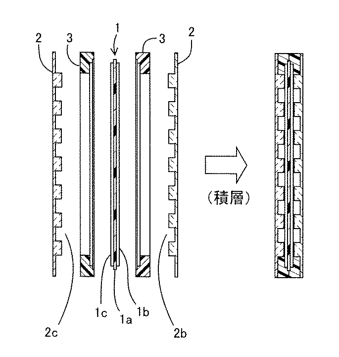
表1の「成膜温度」は、成膜終了時に放射温度計を用いて測定した導電性部材の温度であるが、成膜中の基材の表面温度と同等である。また、「成膜速度」は、得られた導電性部材の非晶質炭素膜の膜厚の実測値を成膜時間で割って算出した。膜厚は、導電性部材について走査型顕微鏡(SEM)による断面観察を行い、複数箇所の膜厚を測定し、その平均値とした。成膜時間は、成膜工程(二工程で行った場合は工程1および工程2)において成膜に要した時間の合計とした。
The “film formation temperature” in Table 1 is the temperature of the conductive member measured using a radiation thermometer at the end of film formation, and is equivalent to the surface temperature of the substrate during film formation. The “deposition rate” was calculated by dividing the measured value of the amorphous carbon film thickness of the obtained conductive member by the deposition time. The film thickness was averaged by conducting cross-sectional observation with a scanning microscope (SEM) on the conductive member and measuring the film thickness at a plurality of locations. The film formation time was defined as the total time required for film formation in the film formation step (step 1 and
<評価>
以下の手順で非晶質炭素膜の組成、接触抵抗および接触角を測定し、組成に対する導電性および親水性を評価した。
<Evaluation>
The composition, contact resistance and contact angle of the amorphous carbon film were measured by the following procedure, and the conductivity and hydrophilicity with respect to the composition were evaluated.
<組成分析>
各導電性部材の非晶質炭素膜の膜組成の測定結果を表2に示した。非晶質炭素膜全体のC、N及びO含有量は、ラザフォード後方散乱法(RBS)により定量した。また、非晶質炭素膜全体のH含有量は、弾性反跳粒子検出法(ERDA)により定量した。ERDAは、2MeVのヘリウムイオンビームを膜表面に照射して、膜からはじき出される水素を半導体検出器により検出し、膜中の水素濃度を測定する方法である。また、Csp2量およびCsp3量は、既に詳説したNMRスペクトルにより定量した。
<Composition analysis>
The measurement results of the film composition of the amorphous carbon film of each conductive member are shown in Table 2. The entire amorphous carbon film C, N and O content was determined by Rutherford backscattering spectroscopy (RBS). Further, the H content of the entire amorphous carbon film was quantified by elastic recoil detection method (ERDA). ERDA is a method of measuring the hydrogen concentration in the film by irradiating the surface of the film with a 2 MeV helium ion beam, detecting hydrogen ejected from the film with a semiconductor detector. Further, the amount of Csp 2 and the amount of Csp 3 were quantified by the NMR spectrum described in detail above.
また、非晶質炭素膜の表層の組成は、アルバック・ファイ株式会社製XPS装置“Quantera SXM”を用い、下記の条件で行った。この条件により、非晶質炭素膜の最表面から2nmまでの深さの表層の組成を測定した。 Further, the composition of the surface layer of the amorphous carbon film was performed using the XPS apparatus “Quantera SXM” manufactured by ULVAC-PHI Co., Ltd. under the following conditions. Under these conditions, the composition of the surface layer having a depth of 2 nm from the outermost surface of the amorphous carbon film was measured.
X線源 : 単色化AlKα
光電子取出角 : 45°
分析領域 : 約200μmφ
パスエネルギー : 26eV
エネルギーステップ: 0.1eV
なお、XPSによりHは検出されないが、C、NおよびO以外の元素はほとんど存在しないため、C量、N量およびO量の合計を100としたときの各元素の含有率が原子個数%(at%)で得られた。測定結果を表2に示した。
X-ray source: Monochromatic AlKα
Photoelectron extraction angle: 45 °
Analysis area: About 200μmφ
Pass energy: 26 eV
Energy step: 0.1 eV
Although H is not detected by XPS, there is almost no element other than C, N, and O. Therefore, the content of each element when the total amount of C, N, and O is 100 is the atomic number% ( at%). The measurement results are shown in Table 2.
<接触角の測定>
各導電性部材に形成された非晶質炭素膜に対して、濡れ性を示す指標である接触角を測定した。図3に、接触角θを示した。接触角の測定は、燃料電池セル内におけるガス拡散層からの水の排出を模擬するために、液滴を所定の高さから膜表面に落下させて動的な要素を加えて行った。具体的には、水平にした非晶質炭素膜の膜表面に対して鉛直上方から水滴を落下させた。落下距離を35mm、液量を2μLとした。水滴を落下させてから1秒後の接触角θ(図3)を接触角計(協和界面科学株式会社製Dropmaster700)を用いて測定した。結果を表2に示した。
<Measurement of contact angle>
A contact angle, which is an index indicating wettability, was measured for the amorphous carbon film formed on each conductive member. FIG. 3 shows the contact angle θ. The contact angle was measured by adding a dynamic element by dropping a droplet from a predetermined height onto the membrane surface in order to simulate the discharge of water from the gas diffusion layer in the fuel cell. Specifically, water droplets were dropped from vertically above the surface of the horizontal amorphous carbon film. The drop distance was 35 mm and the liquid volume was 2 μL. The contact angle θ (FIG. 3) 1 second after dropping the water droplet was measured using a contact angle meter (Dropmaster 700 manufactured by Kyowa Interface Science Co., Ltd.). The results are shown in Table 2.
<接触抵抗の測定>
各導電性部材と、燃料電池用セパレータにおいてガス拡散層を構成するカーボンペーパーと、の接触抵抗を測定した。
<Measurement of contact resistance>
The contact resistance between each conductive member and the carbon paper constituting the gas diffusion layer in the fuel cell separator was measured.
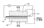
接触抵抗の測定は、図4に示すように、導電性部材10の非晶質炭素膜上にカーボンペーパー31を載置し、2枚の銅板32により挟持した。銅板32は、導電性部材10およびカーボンペーパー31に接触する接触面が金めっきされたものを用いた。このとき、導電性部材10の非晶質炭素膜とカーボンペーパー31とが接触する接触面の面積は、2cm×2cmであった。2枚の銅板32には、ロードセルにより1.47MPaの荷重が、接触面に対して垂直に負荷された。この状態で、2枚の銅板32の間に低電流DC電源により1Aの直流電流を流した。荷重負荷の開始から60秒後における導電性部材10とカーボンペーパー31との電位差を測定して電気抵抗値を算出し、これを接触抵抗値とした。測定結果を表2に示した。
As shown in FIG. 4, the contact resistance was measured by placing a
#C1〜#C3はピリジンガスに対する窒素ガスのガス流量比を変更せずに、#01〜#04は工程1と工程2とでピリジンガスに対する窒素ガスのガス流量比を変更させて、作製された導電性部材であった。いずれの導電性部材も、非晶質炭素膜の全体組成から,体積抵抗が低く導電性に優れていることが推測された。
# C1 to # C3 are manufactured by changing the gas flow rate ratio of nitrogen gas to pyridine gas in
#C1は、少ないガス流量(50sccm/m2)でガス流量比を変更せずに非晶質炭素膜を成膜して得られた導電性部材である。表層のO含有率が2at%であることから、表面の酸化はほとんど無かった。そのため、接触抵抗が非常に小さかったが、接触角θが非常に大きく親水性が不十分であった。なお、#C1において非晶質炭素膜の全体組成のO量が「0」であるのは、膜全体としてみたときのOの存在割合が0に極近かったからである。 # C1 is a conductive member obtained by forming an amorphous carbon film with a small gas flow rate (50 sccm / m 2 ) and without changing the gas flow rate ratio. Since the O content of the surface layer was 2 at%, the surface was hardly oxidized. Therefore, although the contact resistance was very small, the contact angle θ was very large and the hydrophilicity was insufficient. The reason why the amount of O in the entire composition of the amorphous carbon film in “# C1” is “0” is that the ratio of O in the whole film is very close to 0.
#C1の作製条件においてガス流量を多くして作製した導電性部材が、#C2および#C3である。非晶質炭素膜の全体組成のO量は4at%に収まったが、表層のO含有率は非常に高かった。これは、チャンバー内に多く存在する反応ガスの分解が不十分であったために膜表面が活性な状態で成膜が終了し、空気中で酸化されやすかったものと推測される。その結果、接触抵抗は非常に大きくなった。表層のO含有率が多くても接触角θが大きかったのは、表面のC−H結合(未分解の有機基に由来)に起因すると推測される。XPSでは表層のHを検出できないが、非晶質炭素膜の全体組成のH量が多いことから考えて、#C2および#C3の表層は、#C1よりも多くのC−H結合が存在すると推測される。このC−H結合が表面の親水性を低下させているものと思われる。また、#C3は、#C2よりも高い温度で成膜したため、H量が低減された。 The conductive members produced by increasing the gas flow rate under the production conditions of # C1 are # C2 and # C3. The amount of O in the total composition of the amorphous carbon film was within 4 at%, but the O content in the surface layer was very high. This is presumably because the reaction gas present in the chamber was not sufficiently decomposed, so that the film formation was completed while the film surface was active and the film was easily oxidized in the air. As a result, the contact resistance became very large. The reason why the contact angle θ is large even when the O content of the surface layer is large is presumed to be due to the surface C—H bonds (derived from undecomposed organic groups). Although XPS cannot detect H on the surface layer, considering that the amount of H in the entire composition of the amorphous carbon film is large, the surface layers of # C2 and # C3 have more C—H bonds than # C1. Guessed. This C—H bond seems to reduce the hydrophilicity of the surface. Moreover, since # C3 was formed at a temperature higher than # C2, the amount of H was reduced.
#C3の作製条件において成膜工程を二工程にして作製した導電性部材が、#01および#02である。工程2を行ったことで、表層のO含有率が16at%から10at%以下に低減された。これは、#01および#02の非晶質炭素膜にN量の多い表層が形成されたことで、空気中での膜表面の酸化が抑制されたものと推測される。#01および#02における表層のO含有率は、#C1と比較すると多かった。そのため、#01および#02の接触抵抗および接触角θは、セパレータの機能として十分な値を示した。表層の酸素含有率が5〜10at%であっても接触抵抗が小さかったのは、十分な量のNの存在によるものである。
# 01 and # 02 are conductive members produced by forming the film-forming process in two steps under the production conditions of # C3. By performing
#03および#04は、反応ガスのガス流量をさらに増大させて作製した導電性部材である。成膜時のガス流量が1000sccm/m2であっても、工程2において形成された非晶質炭素膜の表面部により、膜表面の酸化が抑制された。その結果、#03および#04は、低接触抵抗と親水性を両立した。
# 03 and # 04 are conductive members manufactured by further increasing the gas flow rate of the reaction gas. Even when the gas flow rate during film formation was 1000 sccm / m 2 , oxidation of the film surface was suppressed by the surface portion of the amorphous carbon film formed in
また、表1に記載の各導電性部材の接触角θより、酸素により非晶質炭素膜表面が終端されると、表面の親水性が高まる(θが小さくなる)傾向がわかった。しかし、非晶質炭素膜に水素を多く含む場合には、親水性が低減(θが大きく)された。親水性に対するC−H結合の影響も考慮すると、非晶質炭素膜全体に含まれるH量を15at%以下さらには13at%以下とすることで、非晶質炭素膜の表面の親水性を確保できることがわかった。 Further, from the contact angle θ of each conductive member shown in Table 1, it was found that when the surface of the amorphous carbon film was terminated by oxygen, the hydrophilicity of the surface increased (θ decreased). However, when the amorphous carbon film contains a large amount of hydrogen, the hydrophilicity is reduced (θ is increased). Considering the influence of C—H bond on the hydrophilicity, the hydrophilicity of the surface of the amorphous carbon film is ensured by setting the amount of H contained in the entire amorphous carbon film to 15 at% or less, further 13 at% or less. I knew it was possible.
さらに、成膜後の非晶質炭素膜の表面の酸化を抑制するためには、表層のN含有率を10at%以上とすることが、接触抵抗の低減の観点からも最適であることがわかった。 Furthermore, in order to suppress the oxidation of the surface of the amorphous carbon film after film formation, it is found that the N content of the surface layer is optimally 10 at% or more from the viewpoint of reducing contact resistance. It was.
つまり、非晶質炭素膜の表層に含まれるNおよびOの含有率を最適な範囲とすることで、非晶質炭素膜の表面に、燃料電池用セパレータに適した接触抵抗および濡れ性が付与されることがわかった。 In other words, by making the content of N and O contained in the surface layer of the amorphous carbon film within the optimum range, contact resistance and wettability suitable for a fuel cell separator are imparted to the surface of the amorphous carbon film. I found out that
Claims (13)
ラザフォード後方散乱法及び弾性反跳粒子検出法によって非晶質炭素膜全体を測定した時に検出される水素が30at%以下、窒素が20at%以下および酸素が3at%以下であり、
固体NMRによって非晶質炭素膜全体を測定した時に検出される炭素量につき、該炭素の全体量を100at%としたときに、sp2混成軌道をもつ炭素量が70at%以上100at%未満であり、
窒素および酸素が膜表面側に濃化して存在し、X線光電子分光法によって表層から検出される酸素の含有率が4at%以上15at%以下、窒素の含有率が10at%以上30at%以下であることを特徴とする非晶質炭素膜。 An amorphous carbon film containing carbon as a main component and containing hydrogen , nitrogen and oxygen,
When the entire amorphous carbon film is measured by Rutherford backscattering method and elastic recoil detection method, hydrogen is 30 at% or less, nitrogen is 20 at% or less, and oxygen is 3 at% or less,
Regarding the amount of carbon detected when the entire amorphous carbon film is measured by solid-state NMR, the amount of carbon having sp 2 hybrid orbital is 70 at% or more and less than 100 at% when the total amount of the carbon is 100 at%. The
Nitrogen and oxygen are concentrated on the film surface side, the oxygen content detected from the surface layer by X-ray photoelectron spectroscopy is 4 at% to 15 at%, and the nitrogen content is 10 at% to 30 at% An amorphous carbon film characterized by the above.
前記非晶質炭素膜は、第一成膜工程および該第一成膜工程後の第二成膜工程を経て成膜され、
前記第二成膜工程は、前記炭素含有ガスに対する前記窒素ガスのガス流量比が、前記第一成膜工程における該ガス流量比よりも大きくなるように前記反応容器に前記反応ガスを導入して行うことを特徴とする非晶質炭素膜の形成方法。 In a reaction vessel containing a substrate, selected and nitrogen gas from a nitrogen-containing heterocyclic compound gas containing carbon and N with gas and sp 2 hybridized carbon ring compounds containing carbon having sp 2 hybrid orbital A plasma CVD method for generating a plasma by introducing a reactive gas containing at least one carbon-containing gas and forming the amorphous carbon film according to any one of claims 1 to 5 on the surface of the substrate A method for forming an amorphous carbon film by:
The amorphous carbon film is formed through a first film formation step and a second film formation step after the first film formation step,
In the second film formation step, the reaction gas is introduced into the reaction vessel so that a gas flow rate ratio of the nitrogen gas to the carbon-containing gas is larger than the gas flow rate ratio in the first film formation step. A method for forming an amorphous carbon film, comprising:
前記非晶質炭素膜は、請求項1〜5のいずれかに記載の非晶質炭素膜であることを特徴とする燃料電池用セパレータ。 A fuel cell separator comprising a metal base material and an amorphous carbon film covering at least the surface of the base material facing the electrode,
The fuel cell separator according to claim 1, wherein the amorphous carbon film is the amorphous carbon film according to claim 1.
Priority Applications (5)
| Application Number | Priority Date | Filing Date | Title |
|---|---|---|---|
| JP2012016256A JP5378552B2 (en) | 2012-01-30 | 2012-01-30 | Amorphous carbon film, method for forming amorphous carbon film, conductive member provided with amorphous carbon film, and separator for fuel cell |
| CN201380007324.1A CN104080945B (en) | 2012-01-30 | 2013-01-25 | Amorphous carbon film, method of forming amorphous carbon film, conductive member provided with amorphous carbon film, and fuel cell separator |
| US14/374,725 US10283785B2 (en) | 2012-01-30 | 2013-01-25 | Amorphous carbon film, process for forming amorphous carbon film, electrically conductive member and fuel cell bipolar plate having amorphous carbon film |
| EP13743187.0A EP2811049B1 (en) | 2012-01-30 | 2013-01-25 | Amorphous carbon film, method for producing amorphous carbon film, conductive member provided with amorphous carbon film, and fuel cell separator |
| PCT/JP2013/000369 WO2013114836A1 (en) | 2012-01-30 | 2013-01-25 | Amorphous carbon film, method for producing amorphous carbon film, conductive member provided with amorphous carbon film, and fuel cell separator |
Applications Claiming Priority (1)
| Application Number | Priority Date | Filing Date | Title |
|---|---|---|---|
| JP2012016256A JP5378552B2 (en) | 2012-01-30 | 2012-01-30 | Amorphous carbon film, method for forming amorphous carbon film, conductive member provided with amorphous carbon film, and separator for fuel cell |
Publications (2)
| Publication Number | Publication Date |
|---|---|
| JP2013155406A JP2013155406A (en) | 2013-08-15 |
| JP5378552B2 true JP5378552B2 (en) | 2013-12-25 |
Family
ID=48904885
Family Applications (1)
| Application Number | Title | Priority Date | Filing Date |
|---|---|---|---|
| JP2012016256A Expired - Fee Related JP5378552B2 (en) | 2012-01-30 | 2012-01-30 | Amorphous carbon film, method for forming amorphous carbon film, conductive member provided with amorphous carbon film, and separator for fuel cell |
Country Status (5)
| Country | Link |
|---|---|
| US (1) | US10283785B2 (en) |
| EP (1) | EP2811049B1 (en) |
| JP (1) | JP5378552B2 (en) |
| CN (1) | CN104080945B (en) |
| WO (1) | WO2013114836A1 (en) |
Families Citing this family (21)
| Publication number | Priority date | Publication date | Assignee | Title |
|---|---|---|---|---|
| JP6160584B2 (en) * | 2014-09-19 | 2017-07-12 | トヨタ自動車株式会社 | Manufacturing method of fuel cell separator |
| KR20160039739A (en) * | 2014-10-01 | 2016-04-12 | 삼성전자주식회사 | Method for forming hard mask layer and method for manufacturing semiconductor device using the same |
| JP6160877B2 (en) | 2015-04-13 | 2017-07-12 | トヨタ自動車株式会社 | Manufacturing method of fuel cell separator and fuel cell separator |
| JP7017218B2 (en) * | 2016-09-21 | 2022-02-08 | 国立大学法人山口大学 | Amorphous carbon manufacturing method and amorphous carbon |
| DE102017202679A1 (en) * | 2017-02-20 | 2018-08-23 | Fraunhofer-Gesellschaft zur Förderung der angewandten Forschung e.V. | Bipolar plate for electrochemical cells and a manufacturing method |
| US11192788B2 (en) | 2017-02-24 | 2021-12-07 | National University Of Singapore | Two-dimensional amorphous carbon coating and methods of growing and differentiating stem cells |
| JP6856012B2 (en) | 2017-12-14 | 2021-04-07 | トヨタ自動車株式会社 | Separator for fuel cells |
| CN108390075B (en) * | 2018-01-24 | 2019-04-02 | 上海交通大学 | Anticorrosive conductive film and its pulsed bias alternating magnetron sputtering deposition method and application |
| JP6610842B1 (en) * | 2018-02-21 | 2019-11-27 | 日本製鉄株式会社 | Titanium material, separator, cell, and fuel cell |
| JP7217055B2 (en) * | 2018-07-30 | 2023-02-02 | ナショナル ユニバーシティー オブ シンガポール | Proton-conducting two-dimensional amorphous carbon films for gas membrane and fuel cell applications |
| CN109853085B (en) * | 2018-12-13 | 2021-08-06 | 大连理工大学 | A method for regulating the conductance of composite nanofibers of amorphous carbon-reduced graphene oxide-cobalt tetroxide-wrapped structure |
| CN109913850B (en) * | 2019-03-07 | 2021-07-23 | 浙江工业大学 | A kind of substrate coated with composite film and its preparation method and application |
| CN110747447A (en) * | 2019-09-11 | 2020-02-04 | 江苏菲沃泰纳米科技有限公司 | Electronic equipment outer cover enhanced nano film and preparation method and application thereof |
| KR20220167795A (en) | 2020-03-10 | 2022-12-21 | 내셔널 유니버시티 오브 싱가포르 | A seed layer, a heterostructure including the seed layer, and a method of forming a material layer using the seed layer |
| US12221690B2 (en) * | 2020-03-31 | 2025-02-11 | Toto Ltd. | Sanitary equipment part |
| JP2023012621A (en) * | 2021-07-14 | 2023-01-26 | 東京エレクトロン株式会社 | Film deposition method and plasma treatment apparatus |
| CN113640172B (en) * | 2021-08-25 | 2024-05-07 | 北京建筑大学 | Device and method for testing film forming rate of polymer emulsion |
| FR3126428B1 (en) * | 2021-08-31 | 2026-02-27 | Hydromecanique & Frottement | Carbon deposition process on a substrate |
| EP4191715A1 (en) | 2021-12-01 | 2023-06-07 | Federal-Mogul Burscheid GmbH | Bipolar plate for fuel cell |
| US20230203721A1 (en) * | 2021-12-28 | 2023-06-29 | NanoTubeTec Co., LTD | Conductive fabric and manufacturing method thereof |
| FR3146695A1 (en) | 2023-03-15 | 2024-09-20 | Hydromecanique Et Frottement | Part coated with a carbon-based layer |
Family Cites Families (15)
| Publication number | Priority date | Publication date | Assignee | Title |
|---|---|---|---|---|
| DE69322907T2 (en) * | 1992-07-24 | 1999-05-27 | Matsushita Electric Industrial Co., Ltd., Kadoma, Osaka | Magnetic recording medium and its manufacturing process |
| JP3208972B2 (en) * | 1993-04-13 | 2001-09-17 | 松下電器産業株式会社 | Magnetic recording media |
| JP3795145B2 (en) * | 1996-09-04 | 2006-07-12 | 松下電器産業株式会社 | Growth method of silicon carbide |
| JP2000067881A (en) | 1998-08-24 | 2000-03-03 | Honda Motor Co Ltd | Fuel cell separator |
| JP2002038268A (en) | 2000-05-19 | 2002-02-06 | Sanyo Electric Co Ltd | Carbon coating and manufacturing method |
| JP4929531B2 (en) | 2001-04-27 | 2012-05-09 | 住友電気工業株式会社 | Conductive hard carbon film |
| JP4409192B2 (en) | 2003-03-25 | 2010-02-03 | 独立行政法人科学技術振興機構 | Amorphous carbon film molded body and method for producing the same |
| JP2005093172A (en) | 2003-09-16 | 2005-04-07 | Nippon Steel Corp | Fuel cell separator and fuel cell |
| US8119242B2 (en) * | 2006-05-22 | 2012-02-21 | Kabushiki Kaisha Toyota Chuo Kenkyusho | Amorphous carbon film, process for forming amorphous carbon film, conductive member provided with amorphous carbon film, and fuel cell separator |
| JP5217243B2 (en) * | 2006-05-22 | 2013-06-19 | 株式会社豊田中央研究所 | Amorphous carbon film, method for forming amorphous carbon film, conductive member provided with amorphous carbon film, and separator for fuel cell |
| US8758957B2 (en) * | 2008-07-29 | 2014-06-24 | GM Global Technology Operations LLC | Graphene coated SS bipolar plates |
| JP2011108547A (en) | 2009-11-19 | 2011-06-02 | Toyota Motor Corp | Fuel cell |
| WO2011077755A1 (en) * | 2009-12-25 | 2011-06-30 | トヨタ自動車株式会社 | Separator for fuel cell and method for producing same |
| US8999604B2 (en) * | 2009-12-25 | 2015-04-07 | Kabushiki Kaisha Toyota Chuo Kenkyusho | Oriented amorphous carbon film and process for forming the same |
| JP5042343B2 (en) * | 2010-06-18 | 2012-10-03 | 株式会社豊田中央研究所 | Film forming method and film forming apparatus |
-
2012
- 2012-01-30 JP JP2012016256A patent/JP5378552B2/en not_active Expired - Fee Related
-
2013
- 2013-01-25 WO PCT/JP2013/000369 patent/WO2013114836A1/en not_active Ceased
- 2013-01-25 EP EP13743187.0A patent/EP2811049B1/en not_active Not-in-force
- 2013-01-25 US US14/374,725 patent/US10283785B2/en not_active Expired - Fee Related
- 2013-01-25 CN CN201380007324.1A patent/CN104080945B/en not_active Expired - Fee Related
Also Published As
| Publication number | Publication date |
|---|---|
| US10283785B2 (en) | 2019-05-07 |
| CN104080945B (en) | 2016-08-24 |
| EP2811049B1 (en) | 2016-11-23 |
| EP2811049A1 (en) | 2014-12-10 |
| EP2811049A4 (en) | 2015-12-16 |
| CN104080945A (en) | 2014-10-01 |
| US20140356764A1 (en) | 2014-12-04 |
| JP2013155406A (en) | 2013-08-15 |
| WO2013114836A1 (en) | 2013-08-08 |
Similar Documents
| Publication | Publication Date | Title |
|---|---|---|
| JP5378552B2 (en) | Amorphous carbon film, method for forming amorphous carbon film, conductive member provided with amorphous carbon film, and separator for fuel cell | |
| JP5217243B2 (en) | Amorphous carbon film, method for forming amorphous carbon film, conductive member provided with amorphous carbon film, and separator for fuel cell | |
| US8119242B2 (en) | Amorphous carbon film, process for forming amorphous carbon film, conductive member provided with amorphous carbon film, and fuel cell separator | |
| JP5420530B2 (en) | Fuel cell separator and method for producing the same | |
| JP5321576B2 (en) | Oriented amorphous carbon film and method for forming the same | |
| Son et al. | Enhanced electrochemical properties of the DLC films with an arc interlayer, nitrogen doping and annealing | |
| Anagri et al. | Nanocomposite coatings based on graphene and siloxane polymers deposited by atmospheric pressure plasma. Application to corrosion protection of steel | |
| Li et al. | Corrosion and conductivity behavior of titanium-doped amorphous carbon film coated SS316L in the environment of PEMFCs | |
| US20130341204A1 (en) | Carbon Electrode Devices for Use with Liquids and Associated Methods | |
| JP2010248572A (en) | Titanium-based material, method for producing the same, and fuel cell separator | |
| Han et al. | Corrosion Resistance of DLC Film‐Coated SUS316L Steel Prepared by Ion Beam Enhanced Deposition | |
| JP4150789B2 (en) | Amorphous carbon nitride film and manufacturing method thereof | |
| JP2012089460A (en) | Separator for fuel cell and plasma processing apparatus therefor | |
| Rashtchi et al. | Performance of a PEM fuel cell using electroplated Ni–Mo and Ni–Mo–P stainless steel bipolar plates | |
| Mori et al. | Amorphous carbon coated stainless separator for PEFCs | |
| An et al. | Effect of the energy of hydrocarbon ions on diamond-like carbon films deposited on alumina microparticles through repeated pulsed discharge in hollow cathode with methane gas | |
| JP2013004511A (en) | Fuel cell separator and method for manufacturing the same | |
| JP2012146616A (en) | Fuel cell separator and method for producing the same | |
| Yang et al. | Sputtering power-dependent microstructure and corrosion behavior of Ti-doped TiC/α-C coatings for PEMFC bipolar plates | |
| KR20100088346A (en) | Method for manufacturing chromium nitride hydrocarbon thin film for fuel cell metal separator and product | |
| JP2006152338A (en) | Diamond-coated electrode and manufacturing method thereof |
Legal Events
| Date | Code | Title | Description |
|---|---|---|---|
| A521 | Request for written amendment filed |
Free format text: JAPANESE INTERMEDIATE CODE: A523 Effective date: 20130620 |
|
| TRDD | Decision of grant or rejection written | ||
| A01 | Written decision to grant a patent or to grant a registration (utility model) |
Free format text: JAPANESE INTERMEDIATE CODE: A01 Effective date: 20130903 |
|
| A61 | First payment of annual fees (during grant procedure) |
Free format text: JAPANESE INTERMEDIATE CODE: A61 Effective date: 20130925 |
|
| R150 | Certificate of patent or registration of utility model |
Ref document number: 5378552 Country of ref document: JP Free format text: JAPANESE INTERMEDIATE CODE: R150 Free format text: JAPANESE INTERMEDIATE CODE: R150 |
|
| R250 | Receipt of annual fees |
Free format text: JAPANESE INTERMEDIATE CODE: R250 |
|
| R250 | Receipt of annual fees |
Free format text: JAPANESE INTERMEDIATE CODE: R250 |
|
| R250 | Receipt of annual fees |
Free format text: JAPANESE INTERMEDIATE CODE: R250 |
|
| R250 | Receipt of annual fees |
Free format text: JAPANESE INTERMEDIATE CODE: R250 |
|
| R250 | Receipt of annual fees |
Free format text: JAPANESE INTERMEDIATE CODE: R250 |
|
| R250 | Receipt of annual fees |
Free format text: JAPANESE INTERMEDIATE CODE: R250 |
|
| LAPS | Cancellation because of no payment of annual fees |