JP5376839B2 - Erase method for nonvolatile memory device - Google Patents
Erase method for nonvolatile memory device Download PDFInfo
- Publication number
- JP5376839B2 JP5376839B2 JP2008153152A JP2008153152A JP5376839B2 JP 5376839 B2 JP5376839 B2 JP 5376839B2 JP 2008153152 A JP2008153152 A JP 2008153152A JP 2008153152 A JP2008153152 A JP 2008153152A JP 5376839 B2 JP5376839 B2 JP 5376839B2
- Authority
- JP
- Japan
- Prior art keywords
- voltage
- memory cell
- post
- dummy
- normal
- Prior art date
- Legal status (The legal status is an assumption and is not a legal conclusion. Google has not performed a legal analysis and makes no representation as to the accuracy of the status listed.)
- Active
Links
Images


Classifications
-
- G—PHYSICS
- G11—INFORMATION STORAGE
- G11C—STATIC STORES
- G11C16/00—Erasable programmable read-only memories
- G11C16/02—Erasable programmable read-only memories electrically programmable
- G11C16/06—Auxiliary circuits, e.g. for writing into memory
- G11C16/10—Programming or data input circuits
- G11C16/14—Circuits for erasing electrically, e.g. erase voltage switching circuits
- G11C16/16—Circuits for erasing electrically, e.g. erase voltage switching circuits for erasing blocks, e.g. arrays, words, groups
-
- G—PHYSICS
- G11—INFORMATION STORAGE
- G11C—STATIC STORES
- G11C16/00—Erasable programmable read-only memories
- G11C16/02—Erasable programmable read-only memories electrically programmable
- G11C16/06—Auxiliary circuits, e.g. for writing into memory
- G11C16/10—Programming or data input circuits
- G11C16/14—Circuits for erasing electrically, e.g. erase voltage switching circuits
-
- G—PHYSICS
- G11—INFORMATION STORAGE
- G11C—STATIC STORES
- G11C16/00—Erasable programmable read-only memories
- G11C16/02—Erasable programmable read-only memories electrically programmable
- G11C16/06—Auxiliary circuits, e.g. for writing into memory
- G11C16/30—Power supply circuits
-
- G—PHYSICS
- G11—INFORMATION STORAGE
- G11C—STATIC STORES
- G11C16/00—Erasable programmable read-only memories
- G11C16/02—Erasable programmable read-only memories electrically programmable
- G11C16/06—Auxiliary circuits, e.g. for writing into memory
- G11C16/34—Determination of programming status, e.g. threshold voltage, overprogramming or underprogramming, retention
Abstract
Description
本発明は、半導体メモリ装置に係り、特に、不揮発性メモリ装置に関する。 The present invention relates to a semiconductor memory device, and more particularly to a nonvolatile memory device.
半導体メモリ装置は、DRAM(Dynamic Random Access Memory)及びSRAM(Static Random Access Memory)のように、電源が切れるとデータを失い、かつデータの入出力が速い揮発性メモリ装置と、一度データを入力すれば、その状態を維持し、データの入出力が揮発性メモリに比べて相対的に遅い不揮発性メモリ装置とに大別される。不揮発性メモリ装置は、ROM(Read Only Memory)、PROM(Programmable ROM)、EPROM(Erasable PROM)及びEEPROM(Electrically EPROM)に分類される。EEPROMまたは一括消去機能を有するフラッシュEEPROM(以下、フラッシュメモリという)は、フローティングゲートと制御ゲートとが積層されたスタック型ゲート構造を有する。 A semiconductor memory device, such as a DRAM (Dynamic Random Access Memory) and SRAM (Static Random Access Memory), loses data when the power is turned off, and inputs data once with a volatile memory device that inputs and outputs data quickly. For example, it is roughly classified into a non-volatile memory device that maintains this state and is relatively slow in data input / output compared to a volatile memory. Non-volatile memory devices are classified into ROM (Read Only Memory), PROM (Programmable ROM), EPROM (Erasable PROM), and EEPROM (Electrically EPROM). An EEPROM or a flash EEPROM having a batch erase function (hereinafter referred to as a flash memory) has a stacked gate structure in which a floating gate and a control gate are stacked.
フラッシュメモリ装置のメモリアレイは、ストリングを基本単位とし、多数のストリングを備える。このストリングは、セレクトトランジスタと多数のメモリセルとが直列に接続された構造よりなる。この場合、フラッシュメモリ装置は、ドレインセレクトラインに隣接したワードラインに連結されたメモリセル及びソースセレクトラインに隣接したワードラインに連結されたメモリセルでプログラム速度が落ちる問題が発生した。この問題点を解決するために、最近では、ストリングにダミーワードラインに連結されるメモリセルを追加する構造が使われている。ダミーワードラインを備えるフラッシュメモリ装置の実施形態については、特許文献1に開示されている。 A memory array of a flash memory device has a string as a basic unit and includes a large number of strings. This string has a structure in which a select transistor and a large number of memory cells are connected in series. In this case, the flash memory device has a problem that the program speed is reduced in the memory cells connected to the word line adjacent to the drain select line and the memory cells connected to the word line adjacent to the source select line. In order to solve this problem, recently, a structure in which a memory cell connected to a dummy word line is added to a string has been used. An embodiment of a flash memory device having a dummy word line is disclosed in Patent Document 1.
フラッシュメモリ装置の消去動作は、プレプログラム動作、メイン消去動作及びポストプログラム動作に大別される。プレプログラム動作は、次に行う消去動作時に過度に消去されるメモリセルの発生を防止するために、正常的なプログラム動作と同じバイアス条件を利用して行われる。消去されるメモリセルは、何れもプレプログラムされる。プレプログラム以後にセクタの全てのメモリセルがオン−セル状態を有するように、メイン消去動作が行われる。メイン消去動作が開始されれば、セクタ内の全てのメモリセルが同時に消去される。最後に、メイン消去動作によって過度に消去されたメモリセルを治癒するために、ポストプログラム動作が行われる。ポストプログラム動作は、バイアス条件を除外すれば、プレプログラム動作と同一に行われる。 The erase operation of the flash memory device is roughly divided into a pre-program operation, a main erase operation, and a post-program operation. The pre-program operation is performed using the same bias condition as the normal program operation in order to prevent generation of memory cells that are excessively erased during the next erase operation. Any memory cell to be erased is preprogrammed. The main erase operation is performed so that all the memory cells in the sector have an on-cell state after the pre-programming. When the main erase operation is started, all the memory cells in the sector are erased simultaneously. Finally, a post program operation is performed to cure memory cells that have been excessively erased by the main erase operation. The post program operation is performed in the same manner as the pre program operation except for the bias condition.
ダミーワードラインを備えたフラッシュメモリ装置でポストプログラム動作を行う場合、従来は、ダミーワードラインに連結されたダミーメモリセル及びノーマルワードラインに連結されたノーマルメモリセルに対して区別なしに一括的にポストプログラム動作を行った。すなわち、ポストプログラムを行った結果、ノーマルメモリセル及びダミーメモリセルは、同じしきい電圧を有する。この場合、消去動作が終了した後にプログラム動作を行うとき、ターンオフされねばならないダミーメモリセルがターンオンされる場合が発生して、ノーマルメモリセルのプログラムを妨害する場合が発生する。
本発明が解決しようとする技術的課題は、ノーマルワードラインに連結されたノーマルメモリセル及びダミーワードラインに連結されたダミーメモリセルに対して別途にポストプログラムを行う不揮発性メモリ装置の消去方法を提供することである。 The technical problem to be solved by the present invention is to provide a method of erasing a nonvolatile memory device in which post-programming is separately performed on a normal memory cell connected to a normal word line and a dummy memory cell connected to a dummy word line. Is to provide.
前記課題を達成するための本発明の実施形態による不揮発性メモリ装置の消去方法は、不揮発性メモリ装置でポストプログラムを行う消去方法において、ダミーメモリセルに対してポストプログラムを行うステップ、第1電圧を利用して前記ダミーメモリセルのしきい電圧を検証するステップ、ノーマルメモリセルに対して前記ポストプログラムを行うステップ及び第2電圧を利用して前記ノーマルメモリセルのしきい電圧を検証するステップを含み、前記第1電圧は、前記第2電圧とは相異なる電圧レベルを有しうる。 An erasing method of a non-volatile memory device according to an embodiment of the present invention for achieving the above object includes a step of performing a post program on a dummy memory cell in the erasing method of performing a post program in the non-volatile memory device, a first voltage Verifying the threshold voltage of the dummy memory cell using a step, performing the post-programming on the normal memory cell, and verifying the threshold voltage of the normal memory cell using a second voltage. The first voltage may have a voltage level different from that of the second voltage.
前記第1電圧は、前記第2電圧より高い電圧レベルを有することが望ましい。
前記不揮発性メモリ装置の消去方法は、前記ダミーメモリセルのしきい電圧が前記第1電圧より低い場合、前記ダミーメモリセルに対してポストプログラムを再び行うステップをさらに含むことが望ましい。
前記不揮発性メモリ装置の消去方法は、前記ノーマルメモリセルのしきい電圧が前記第2電圧より低い場合、前記ノーマルメモリセルに対してポストプログラムを再び行うステップをさらに含むことが望ましい。
The first voltage may have a higher voltage level than the second voltage.
The erasing method of the non-volatile memory device may further include a step of re-programming the dummy memory cell when the threshold voltage of the dummy memory cell is lower than the first voltage.
The erasing method of the non-volatile memory device may further include a step of re-programming the normal memory cell when the threshold voltage of the normal memory cell is lower than the second voltage.
前記ダミーメモリセルに対してポストプログラムを行うステップは、前記ダミーメモリセルに対して前記ポストプログラムを行うように、前記ダミーメモリセルに連結されたダミーワードラインにプログラム電圧を印加するステップ及び前記ノーマルメモリセルに対して前記ポストプログラムを行わないように、前記ノーマルメモリセルに連結されたノーマルワードラインにパス電圧を印加するステップを含むことが望ましい。 The step of performing a post program on the dummy memory cell includes applying a program voltage to a dummy word line connected to the dummy memory cell so as to perform the post program on the dummy memory cell and the normal. Preferably, the method includes a step of applying a pass voltage to a normal word line connected to the normal memory cell so that the post program is not performed on the memory cell.
前記ノーマルメモリセルに対してポストプログラムを行うステップは、前記ノーマルメモリセルに対して前記ポストプログラムを行うように、前記ノーマルメモリセルに連結されたノーマルワードラインにプログラム電圧を印加するステップ及び前記ダミーメモリセルに対して前記ポストプログラムを行わないように、前記ダミーメモリセルに連結されたダミーワードラインにパス電圧を印加するステップを含むことが望ましい。 The step of performing the post program on the normal memory cell includes the step of applying a program voltage to a normal word line connected to the normal memory cell and the dummy so as to perform the post program on the normal memory cell. Preferably, the method includes a step of applying a pass voltage to a dummy word line connected to the dummy memory cell so that the post program is not performed on the memory cell.
前記ノーマルメモリセルに対して前記ポストプログラムを行うステップ及び前記ノーマルメモリセルのしきい電圧を検証するステップは、前記ダミーメモリセルに対してポストプログラムを行うステップ及び前記ダミーメモリセルのしきい電圧を検証するステップ以前に行われることが望ましい。
前記ダミーメモリセルに対してポストプログラムを行うステップ及び前記ダミーメモリセルのしきい電圧を検証するステップは、前記ノーマルメモリセルに対して前記ポストプログラムを行うステップ及び前記ノーマルメモリセルのしきい電圧を検証するステップ以前に行われることが望ましい。
The step of performing the post program on the normal memory cell and the step of verifying the threshold voltage of the normal memory cell include the step of performing the post program on the dummy memory cell and the threshold voltage of the dummy memory cell. It should be done before the verification step.
The step of performing the post program on the dummy memory cell and the step of verifying the threshold voltage of the dummy memory cell include the step of performing the post program on the normal memory cell and the threshold voltage of the normal memory cell. It should be done before the verification step.
前記ダミーメモリセルに対してポストプログラムを行うステップ及び前記ノーマルメモリセルに対して前記ポストプログラムを行うステップは、前記ノーマルメモリセルのしきい電圧を検証するステップ及び前記ダミーメモリセルのしきい電圧を検証するステップ以前に行われることが望ましい。 The step of performing the post program on the dummy memory cell and the step of performing the post program on the normal memory cell include the step of verifying the threshold voltage of the normal memory cell and the threshold voltage of the dummy memory cell. It should be done before the verification step.
前記課題を達成するための本発明の他の実施形態による不揮発性メモリ装置の消去方法は、不揮発性メモリ装置でポストプログラムを行う消去方法において、第1ダミーメモリセルに対してポストプログラムを行うステップ、第1電圧を利用して前記第1ダミーメモリセルのしきい電圧を検証するステップ、第2ダミーメモリセルに対して前記ポストプログラムを行うステップ、第2電圧を利用して前記第2ダミーメモリセルのしきい電圧を検証するステップ、ノーマルメモリセルに対して前記ポストプログラムを行うステップ及び第3電圧を利用して前記ノーマルメモリセルのしきい電圧を検証するステップを含み、前記第3電圧は、前記第1電圧及び前記第2電圧とは相異なる電圧レベルを有しうる。 According to another embodiment of the present invention, there is provided a non-volatile memory device erasing method for performing post-programming on a first dummy memory cell in an erasing method for performing post-programming in the non-volatile memory device. Verifying a threshold voltage of the first dummy memory cell using a first voltage, performing post-programming on the second dummy memory cell, and using the second voltage to the second dummy memory Verifying a threshold voltage of a cell, performing the post-programming on a normal memory cell, and verifying a threshold voltage of the normal memory cell using a third voltage, wherein the third voltage is The first voltage and the second voltage may have different voltage levels.
前記課題を達成するための本発明のさらに他の実施形態による不揮発性メモリ装置の消去方法は、不揮発性メモリ装置でポストプログラムを行う消去方法において、ノーマルメモリセル及びダミーメモリセルに対してポストプログラムを行うステップ、第1電圧を利用して前記ダミーメモリセルのしきい電圧を検証するステップ、第2電圧を利用して前記ノーマルメモリセルのしきい電圧を検証するステップ及び前記しきい電圧が検証されないダミーメモリセル及び前記しきい電圧が検証されないノーマルメモリセルを含むメモリセルグループに対して前記ポストプログラムを行うステップを含み、前記第1電圧は、前記第2電圧とは相異なる電圧レベルを有しうる。 According to another aspect of the present invention, there is provided an erasing method of a non-volatile memory device, wherein the non-volatile memory device performs post-programming on a normal memory cell and a dummy memory cell. Performing a step of verifying a threshold voltage of the dummy memory cell using a first voltage, verifying a threshold voltage of the normal memory cell using a second voltage, and verifying the threshold voltage. Performing post-programming on a memory cell group including a dummy memory cell that is not tested and a normal memory cell whose threshold voltage is not verified, wherein the first voltage has a voltage level different from that of the second voltage. Yes.
前記課題を達成するための本発明のさらに他の実施形態による不揮発性メモリ装置の消去方法は、不揮発性メモリ装置でポストプログラムを行う消去方法において、ノーマルメモリセル、第1ダミーメモリセル及び第2ダミーメモリセルに対してポストプログラムを行うステップ、第1電圧を利用して前記第1ダミーメモリセルのしきい電圧を検証するステップ、第2電圧を利用して前記第2ダミーメモリセルのしきい電圧を検証するステップ、第3電圧を利用して前記ノーマルメモリセルのしきい電圧を検証するステップ及び前記しきい電圧が検証されない第1ダミーメモリセル、前記しきい電圧が検証されない第2ダミーメモリセル及び前記しきい電圧が検証されないノーマルメモリセルを含むメモリセルグループに対して前記ポストプログラムを行うステップを含み、前記第3電圧は、前記第1電圧及び前記第2電圧とは相異なる電圧レベルを有しうる。 According to another aspect of the present invention, there is provided an erasing method of a non-volatile memory device according to another embodiment of the present invention, wherein the non-volatile memory device performs post-programming in a normal memory cell, a first dummy memory cell, and a second memory cell. Performing a post program on the dummy memory cell; verifying a threshold voltage of the first dummy memory cell using a first voltage; and thresholding the second dummy memory cell using a second voltage. Verifying the voltage, verifying a threshold voltage of the normal memory cell using a third voltage, a first dummy memory cell in which the threshold voltage is not verified, and a second dummy memory in which the threshold voltage is not verified For the memory cell group including cells and normal memory cells whose threshold voltage is not verified. Includes a step of performing grams, the third voltage is said first voltage and said second voltage may have different voltage levels.
本発明による不揮発性メモリ装置の消去方法は、ノーマルメモリセル及びダミーメモリセルに対して別途にポストプログラムを行うことによって、接合ポテンシャルが増加してセルの信頼性を向上させ、ダミーメモリセルのターンオンによるノーマルメモリセルのプログラムを妨害する現象を防止しうる。 According to the non-volatile memory device erasing method of the present invention, by separately performing post-programming on a normal memory cell and a dummy memory cell, the junction potential is increased to improve the reliability of the cell, and the dummy memory cell is turned on. This can prevent a phenomenon that disturbs the programming of the normal memory cell.
本発明と本発明の動作上の利点及び本発明の実施によって達成される目的を十分に理解するためには、本発明の望ましい実施形態を例示する添付図面及び図面に記載された内容を参照しなければならない。
以下、添付した図面を参照して、本発明の望ましい実施形態を説明することによって、本発明を詳細に説明する。各図面に付された同一参照符号は、同一部材を表す。
For a full understanding of the invention and the operational advantages thereof and the objects achieved by the practice of the invention, reference should be made to the accompanying drawings that illustrate preferred embodiments of the invention and the contents described in the drawings. There must be.
Hereinafter, exemplary embodiments of the present invention will be described in detail with reference to the accompanying drawings. The same reference numerals attached to the drawings represent the same members.
図1は、不揮発性半導体メモリ装置の回路図である。
図1では、不揮発性半導体メモリ装置の一つのストリング100を示した。図1を参照すれば、不揮発性半導体メモリ装置、特に、フラッシュメモリ装置の一つのストリング100は、第1セレクトトランジスタGST、第2セレクトトランジスタSST、第1ダミーメモリセルDC1、第2ダミーメモリセルDC2及び複数のノーマルメモリセルC0,…,C30,C31を備える。図1では、32個のメモリセルが直列に連結された場合について示しているが、16個、64個のメモリセルを直列に連結した場合にも、本発明の方法による場合、同じ効果が得られるというのは、当業者に自明な事項である。
FIG. 1 is a circuit diagram of a nonvolatile semiconductor memory device.
FIG. 1 shows one
第1セレクトトランジスタGSTのゲートラインは、第1セレクトラインGSLとなり、第2セレクトトランジスタSSTのゲートラインは、第2セレクトラインSSLとなり、ノーマルメモリセルC0,…,C31のゲートラインは、ノーマルワードラインWL0,…,WL31となる。また、第1ダミーメモリセルDC1のゲートラインは、第1ダミーワードラインDWL1となり、第2ダミーメモリセルDC2のゲートラインは、第2ダミーワードラインDWL2となる。本発明の実施形態によるポストプログラム動作を行う方法については、以下で詳細に説明する。 The gate line of the first select transistor GST becomes the first select line GSL, the gate line of the second select transistor SST becomes the second select line SSL, and the gate lines of the normal memory cells C0,. WL0,..., WL31. In addition, the gate line of the first dummy memory cell DC1 becomes the first dummy word line DWL1, and the gate line of the second dummy memory cell DC2 becomes the second dummy word line DWL2. A method for performing a post program operation according to an embodiment of the present invention will be described in detail below.
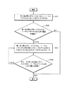
図2は、本発明の実施形態による不揮発性メモリ装置の消去方法を示すフローチャートである。
図2は、不揮発性メモリ装置の消去方法のうち、特にポストプログラム動作を行う方法について示している。図1及び図2を参照して、32個のノーマルメモリセル及び2個のダミーメモリセルが直列に連結されたストリングを有する不揮発性メモリ装置で前記ポストプログラムを行う場合について説明する。一旦、ノーマルワードラインWL0,…,WL31に連結されたノーマルメモリセルC0,…,C31については、ポストプログラムを行わず、ダミーワードラインDWL1,DW2に連結されたダミーメモリセルDC1,DC2に対してポストプログラムを行う(S210)。ダミーメモリセルDC1,DC2に対するポストプログラムが終了すれば、ダミーメモリセルDC1,DC2に対してポストプログラムが正常的に行われたか否かを検証する。すなわち、第1電圧を利用してダミーメモリセルDC1,DC2のしきい電圧を検証する(S220)。前記第1電圧は、ダミーメモリセルDC1,DC2に対して前記ポストプログラムを行って変更しようとするしきい電圧値である。
FIG. 2 is a flowchart illustrating a method for erasing a nonvolatile memory device according to an embodiment of the present invention.
FIG. 2 shows a method for performing a post program operation among the erasing methods of the nonvolatile memory device. Referring to FIGS. 1 and 2, a case where the post program is performed in a nonvolatile memory device having a string in which 32 normal memory cells and two dummy memory cells are connected in series will be described. Once the normal memory cells C0,..., C31 connected to the normal word lines WL0,..., WL31 are not post-programmed, the dummy memory cells DC1, DC2 connected to the dummy word lines DWL1, DW2 are not subjected to post-programming. A post program is performed (S210). When the post program for the dummy memory cells DC1, DC2 is completed, it is verified whether the post program is normally performed for the dummy memory cells DC1, DC2. That is, the threshold voltages of the dummy memory cells DC1 and DC2 are verified using the first voltage (S220). The first voltage is a threshold voltage value to be changed by performing the post program on the dummy memory cells DC1 and DC2.
検証の結果、ダミーメモリセルDC1,DC2のしきい電圧が前記第1電圧より低い場合、ダミーメモリセルDC1,DC2に対して再びポストプログラムを行う(S210)。
前記検証結果、ダミーメモリセルDC1,DC2のしきい電圧が前記第1電圧以上である場合、ノーマルメモリセルC0,…,C31に対してポストプログラムを行う(S230)。ノーマルメモリセルC0,…,C31に対してポストプログラムが終了すれば、ポストプログラムが正常的に行われたか否かを検証する。すなわち、第2電圧を利用してポストプログラムが行われたノーマルメモリセルのしきい電圧を検証する(S240)。第2電圧は、ノーマルメモリセルC0,…,C31に対してポストプログラムを行って変更しようとするしきい電圧値である。第1電圧は、第2電圧より高い電圧レベルを有することが望ましい。
検証の結果、ノーマルメモリセルのしきい電圧が第2電圧より低い場合、ノーマルメモリセルに対して再びポストプログラムを行う(S230)。
If the threshold voltage of the dummy memory cells DC1 and DC2 is lower than the first voltage as a result of the verification, the dummy memory cells DC1 and DC2 are post-programmed again (S210).
As a result of the verification, if the threshold voltages of the dummy memory cells DC1 and DC2 are equal to or higher than the first voltage, the normal memory cells C0,..., C31 are post-programmed (S230). When the post program is completed for the normal memory cells C0,..., C31, it is verified whether or not the post program is normally performed. That is, the threshold voltage of the normal memory cell that has been post-programmed using the second voltage is verified (S240). The second voltage is a threshold voltage value to be changed by performing a post program on the normal memory cells C0,. The first voltage preferably has a higher voltage level than the second voltage.
If the threshold voltage of the normal memory cell is lower than the second voltage as a result of the verification, the normal memory cell is post-programmed again (S230).
図3は、図2の実施形態によるポストプログラムを行う場合、電圧条件を示すテーブルである。
図1ないし図3を参照すれば、ダミーメモリセルDC1,DC2に対してポストプログラムを行うS210の場合、ダミーワードラインDWL1,DWL2には、プログラム電圧Vpgmを印加し、ノーマルワードラインWL0,…,WL31には、パス電圧Vpassを印加する。プログラム電圧Vpgmは、ポストプログラムを行うメモリセルのゲートに連結されたワードラインに印加される電圧であって、例えば、25Vの電圧を使用しうる。パス電圧Vpassは、ポストプログラムを行わないメモリセルのゲートに連結されたワードラインに印加される電圧であって、例えば、8Vの電圧を使用しうる。
FIG. 3 is a table showing voltage conditions when the post program according to the embodiment of FIG. 2 is performed.
1 to 3, in the case of S210 in which the dummy memory cells DC1 and DC2 are post-programmed, the program voltage Vpgm is applied to the dummy word lines DWL1 and DWL2, and the normal word lines WL0,. A pass voltage Vpass is applied to WL31. The program voltage Vpgm is a voltage applied to a word line connected to the gate of a memory cell that performs post-programming. For example, a voltage of 25 V can be used. The pass voltage Vpass is a voltage applied to a word line connected to the gate of a memory cell that is not subjected to post-programming, and may be, for example, a voltage of 8V.
第1電圧を利用してダミーメモリセルDC1,DC2のしきい電圧を検証するS220は、ダミーワードラインDWL1,DWL2に第1電圧Vr1を印加し、ノーマルワードラインWL0,…,WL31に第3電圧Vreadを印加する。第3電圧Vreadは、検証しないワードラインに印加される電圧であって、第1電圧Vr1より高い電圧レベルを有することが望ましい。例えば、第3電圧Vreadは、6.5Vでありうる。 In S220 for verifying the threshold voltages of the dummy memory cells DC1, DC2 using the first voltage, the first voltage Vr1 is applied to the dummy word lines DWL1, DWL2, and the third voltage is applied to the normal word lines WL0,. Vread is applied. The third voltage Vread is a voltage applied to an unverified word line, and preferably has a higher voltage level than the first voltage Vr1. For example, the third voltage Vread may be 6.5V.
ダミーメモリセルDC1,DC2に対する検証が完了して、ノーマルメモリセルC0,…,C31に対してポストプログラムを行うS230の場合、S210とは逆に、ノーマルメモリセルC0,…,C31に連結されたノーマルワードラインWL0,…,WL31に対しては、プログラム電圧Vpgmを印加し、ダミーワードラインDWL1,DWL2に対しては、パス電圧Vpassを印加する。第3電圧Vreadは、第2電圧Vr2より高い電圧レベルを有することが望ましい。 In the case of S230 in which the dummy memory cells DC1, DC2 are verified and the normal memory cells C0,..., C31 are post-programmed, they are connected to the normal memory cells C0,. Program voltage Vpgm is applied to normal word lines WL0,..., WL31, and pass voltage Vpass is applied to dummy word lines DWL1, DWL2. The third voltage Vread preferably has a higher voltage level than the second voltage Vr2.
図4は、本発明の他の実施形態による不揮発性メモリ装置の消去方法を示すフローチャートである。
図1、図2及び図4を参照すれば、図4の実施形態は、図2の実施形態と順序を異ならせている。すなわち、図2の実施形態は、ダミーメモリセルDC1,DC2に対して、まずポストプログラム(S210)及び検証(S220)を行った後、ノーマルメモリセルC0,…,C31に対してポストプログラム(S230)及び検証(S240を行った。しかし、図4の実施形態では、ノーマルメモリセルC0,…,C31に対して、まずポストプログラム(S410)を行い、第2電圧を利用してノーマルメモリセルC0,…,C31のしきい電圧を検証する(S420)。前記ノーマルメモリセルC0,…,C31に対してポストプログラム及び検証を完了した後、ダミーメモリセルDC1,DC2に対してポストプログラム(S430)を行い、第1電圧を利用してダミーメモリセルDC1,DC2のしきい電圧を検証する(S440)。前記各ステップでの動作は、図2の場合と同一であるので、以下では詳細な説明を省略する。
FIG. 4 is a flowchart illustrating a method for erasing a nonvolatile memory device according to another embodiment of the present invention.
Referring to FIGS. 1, 2 and 4, the embodiment of FIG. 4 differs in order from the embodiment of FIG. That is, in the embodiment shown in FIG. 2, first, post program (S210) and verification (S220) are performed on the dummy memory cells DC1 and DC2, and then post program (S230) is performed on the normal memory cells C0,. ) And verification (S240. However, in the embodiment of FIG. 4, the normal memory cells C0,..., C31 are first post-programmed (S410), and the normal memory cell C0 is utilized using the second voltage. ,..., C31 threshold voltage is verified (S420) After the completion of post-programming and verification for the normal memory cells C0, ..., C31, the dummy memory cells DC1 and DC2 are post-programmed (S430). And the threshold voltages of the dummy memory cells DC1 and DC2 are verified using the first voltage (S44). ). The operation in each step is omitted are the same as in FIG. 2, a detailed explanation will be omitted herein.
図5は、本発明のさらに他の実施形態による不揮発性メモリ装置の消去方法を示すフローチャートである。
図6は、図5の実施形態によるポストプログラムを行う場合、電圧条件を示すテーブルである。
FIG. 5 is a flowchart illustrating a method for erasing a nonvolatile memory device according to another embodiment of the present invention.
FIG. 6 is a table showing voltage conditions when the post program according to the embodiment of FIG. 5 is performed.
図1、図5及び図6を参照すれば、図5の実施形態は、ダミーメモリセルDC1,DC2のそれぞれが異なるしきい電圧を有するようにポストプログラムを行う。すなわち、第1ダミーワードラインDWL1に連結された第1ダミーメモリセルDC1に対して、まずポストプログラムを行う(S510)。第1ダミーワードラインDWL1には、プログラム電圧Vpgmを印加し、第2ダミーワードラインDWL2及びノーマルワードラインWL0,…,WL31には、パス電圧Vpassを印加する。このポストプログラム動作が完了すれば、第1電圧Vr1’を利用して第1ダミーメモリセルDC1のしきい電圧を検証する(S520)。すなわち、第1ダミーワードラインDWL1には、第1電圧Vr1’を印加し、第2ダミーワードラインDWL2及びノーマルワードラインWL0,…,WL31には、第4電圧Vreadを印加する。第4電圧Vreadは、図3の第3電圧Vreadと同じ電圧レベルを有する。 Referring to FIGS. 1, 5, and 6, the embodiment of FIG. 5 performs post-programming so that each of the dummy memory cells DC <b> 1 and DC <b> 2 has a different threshold voltage. That is, first, a post program is performed on the first dummy memory cell DC1 connected to the first dummy word line DWL1 (S510). The program voltage Vpgm is applied to the first dummy word line DWL1, and the pass voltage Vpass is applied to the second dummy word line DWL2 and the normal word lines WL0,. When the post program operation is completed, the threshold voltage of the first dummy memory cell DC1 is verified using the first voltage Vr1 '(S520). That is, the first voltage Vr1 'is applied to the first dummy word line DWL1, and the fourth voltage Vread is applied to the second dummy word line DWL2 and the normal word lines WL0,. The fourth voltage Vread has the same voltage level as the third voltage Vread of FIG.
検証の結果、第1ダミーメモリセルDC1のしきい電圧が第1電圧Vr1’より低い場合、第1ダミーメモリセルDC1に対して再びポストプログラムを行う(S510)。検証の結果、第1ダミーメモリセルDC1のしきい電圧が第1電圧Vr1以上である場合、第2ダミーメモリセルDC2に対してポストプログラムを行う(S530)。 As a result of the verification, if the threshold voltage of the first dummy memory cell DC1 is lower than the first voltage Vr1 ', the first dummy memory cell DC1 is post-programmed again (S510). As a result of the verification, if the threshold voltage of the first dummy memory cell DC1 is equal to or higher than the first voltage Vr1, post-program is performed on the second dummy memory cell DC2 (S530).
第2ダミーメモリセルDC1に対してポストプログラムを行う場合(S630)、第2ダミーワードラインDWL2には、プログラム電圧Vpgmを印加し、第1ダミーワードラインDWL1及びノーマルワードラインWL0,…,WL31には、パス電圧Vpassを印加する。このポストプログラム動作が完了すれば、第2電圧Vr2’を利用して第2ダミーメモリセルDC2のしきい電圧を検証する(S540)。第2電圧Vr2’は、第2ダミーメモリセルDC2に対してポストプログラムを行って変更しようとするしきい電圧値であって、第1電圧Vr1’と相異なる電圧レベルを有する。第2ダミーワードラインDWL2には、第2電圧Vr2’を印加し、第1ダミーワードラインDWL12及びノーマルワードラインWL0,…,WL31には、第4電圧Vreadを印加する。 When the post program is performed on the second dummy memory cell DC1 (S630), the program voltage Vpgm is applied to the second dummy word line DWL2, and the first dummy word line DWL1 and the normal word lines WL0,. Applies a pass voltage Vpass. When the post program operation is completed, the threshold voltage of the second dummy memory cell DC2 is verified using the second voltage Vr2 '(S540). The second voltage Vr2 'is a threshold voltage value to be changed by performing a post program on the second dummy memory cell DC2, and has a voltage level different from the first voltage Vr1'. A second voltage Vr2 'is applied to the second dummy word line DWL2, and a fourth voltage Vread is applied to the first dummy word line DWL12 and the normal word lines WL0,.
前記検証結果、第2ダミーメモリセルDC2のしきい電圧が第2電圧Vr2’より低い場合、第2ダミーメモリセルDC2に対して再びポストプログラムを行う(S530)。検証の結果、第2ダミーメモリセルDC2のしきい電圧が第2電圧Vr2’以上である場合、それぞれのノーマルメモリセルC0,…,C31に対してポストプログラムを行う(S550)。 As a result of the verification, if the threshold voltage of the second dummy memory cell DC2 is lower than the second voltage Vr2 ', the second dummy memory cell DC2 is post-programmed again (S530). As a result of the verification, if the threshold voltage of the second dummy memory cell DC2 is equal to or higher than the second voltage Vr2 ', post-programming is performed on each of the normal memory cells C0, ..., C31 (S550).
ノーマルメモリセルC0,…,C31に対してポストプログラム(S550)及び検証(S560)を行うステップは、図2の場合と同一であるので、以下では説明を省略する。図6の第3電圧Vr3’は、図2の第2電圧Vr2と同じ電圧レベルを有する。
但し、図5の実施形態では、第1ダミーメモリセルDC1、第2ダミーメモリセルDC2及びノーマルメモリセルの順序でポストプログラム及び検証を行っているが、順序が変わっても同じ効果が得られるということは、当業者に自明な事項である。
The steps for performing the post program (S550) and verification (S560) on the normal memory cells C0,..., C31 are the same as those in FIG. The third voltage Vr3 ′ in FIG. 6 has the same voltage level as the second voltage Vr2 in FIG.
However, in the embodiment of FIG. 5, post-programming and verification are performed in the order of the first dummy memory cell DC1, the second dummy memory cell DC2, and the normal memory cell, but the same effect can be obtained even if the order is changed. This is obvious to those skilled in the art.
図7は、本発明のさらに他の実施形態による不揮発性メモリ装置の消去方法を示すフローチャートである。
図1、図3及び図7を参照すれば、図7の実施形態は、ノーマルメモリセルC0,…,C31及びダミーメモリセルDC1,DC2に対して同時にポストプログラム動作を行う(S710)。すなわち、ダミーワードラインDWL1,DWL2及びノーマルワードラインWL0,…,WL31にプログラム電圧Vpgmを印加する。
FIG. 7 is a flowchart illustrating a method of erasing a nonvolatile memory device according to another embodiment of the present invention.
Referring to FIGS. 1, 3 and 7, the embodiment of FIG. 7 performs a post program operation on the normal memory cells C0,..., C31 and the dummy memory cells DC1 and DC2 simultaneously (S710). That is, the program voltage Vpgm is applied to the dummy word lines DWL1, DWL2 and the normal word lines WL0,.
ポストプログラム動作が完了した後、ダミーメモリセルDC1,DC2及びノーマルメモリセルC0,…,C31に対してポストプログラムが正常的に行われたか否かを検証する(S720)。すなわち、第1電圧Vr1を利用してダミーメモリセルDC1,DC2のしきい電圧を検証し、第2電圧Vr2を利用してノーマルメモリセルC0,…,C31のしきい電圧を検証する。ダミーワードラインDWL1,DWL2に対して検証を行うために、ダミーワードラインDWL1,DWL2には、第1電圧Vr1を印加し、ノーマルワードラインWL0,…,WL31には、第3電圧Vreadを印加する。また、ノーマルワードラインWL0,…,WL31に対して検証を行うために、ノーマルワードラインWL0,…,WL31には、第2電圧Vr2を印加し、ダミーワードラインDWL1,DWL2には、第3電圧Vreadを印加する。 After the post program operation is completed, it is verified whether the post program is normally performed on the dummy memory cells DC1, DC2 and the normal memory cells C0,..., C31 (S720). That is, the threshold voltages of the dummy memory cells DC1, DC2 are verified using the first voltage Vr1, and the threshold voltages of the normal memory cells C0,..., C31 are verified using the second voltage Vr2. In order to verify the dummy word lines DWL1 and DWL2, the first voltage Vr1 is applied to the dummy word lines DWL1 and DWL2, and the third voltage Vread is applied to the normal word lines WL0,. . In order to verify the normal word lines WL0,..., WL31, the second voltage Vr2 is applied to the normal word lines WL0,..., WL31, and the third voltage is applied to the dummy word lines DWL1, DWL2. Vread is applied.
検証の結果、それぞれのしきい電圧が対応する電圧レベルとならないメモリセルに対して再びポストプログラムを行い(S730)、ポストプログラムが正常的に行われたか否かを検証する(S740)。すなわち、第1メモリセルグループのメモリセルに対しては、ポストプログラムを行い、第2メモリセルグループのメモリセルに対しては、ポストプログラムを行わない。第1メモリセルグループは、しきい電圧が第1電圧Vr1より低いダミーメモリセル及びしきい電圧が第2電圧Vr2より低いノーマルメモリセルのうち少なくとも一つを含む。第2メモリセルグループは、しきい電圧が第1電圧Vr1以上であるダミーメモリセル及びしきい電圧が第2電圧Vr2以上であるノーマルメモリセルを含む。 As a result of the verification, the memory cell whose threshold voltage does not reach the corresponding voltage level is again post-programmed (S730), and it is verified whether the post-program has been normally performed (S740). That is, the post program is performed on the memory cells in the first memory cell group, and the post program is not performed on the memory cells in the second memory cell group. The first memory cell group includes at least one of a dummy memory cell having a threshold voltage lower than the first voltage Vr1 and a normal memory cell having a threshold voltage lower than the second voltage Vr2. The second memory cell group includes a dummy memory cell whose threshold voltage is equal to or higher than the first voltage Vr1 and a normal memory cell whose threshold voltage is equal to or higher than the second voltage Vr2.
例えば、検証の結果、ダミーメモリセルDC1,DC2のしきい電圧が第1電圧Vr1となったならば、第1メモリセルグループは、ノーマルメモリセルC0,…,C31を含み、第2メモリセルグループは、ダミーメモリセルDC1,DC2を含む。したがって、第2メモリセルグループのダミーメモリセルDC1,DC2に対しては、再びポストプログラムを行わず、第1メモリセルグループのノーマルメモリセルC0,…,C31に対してのみ、再びポストプログラムを行う。再びポストプログラムを行った第1メモリセルグループのノーマルメモリセルC0,…,C31に対して検証し、その結果、ノーマルメモリセルC0,…,C31のしきい電圧が第2電圧Vr2以上となったならば、ポストプログラム動作を完了する。 For example, if the threshold voltage of the dummy memory cells DC1 and DC2 becomes the first voltage Vr1 as a result of the verification, the first memory cell group includes the normal memory cells C0,. Includes dummy memory cells DC1, DC2. Therefore, the post program is not performed again on the dummy memory cells DC1 and DC2 of the second memory cell group, and the post program is performed again only on the normal memory cells C0,..., C31 of the first memory cell group. . The normal memory cells C0,..., C31 of the first memory cell group that has been post-programmed again are verified. As a result, the threshold voltage of the normal memory cells C0,. If so, the post program operation is completed.
図8は、本発明のさらに他の実施形態による不揮発性メモリ装置の消去方法を示すフローチャートである。
図1、図6、図7及び図8を参照すれば、図8の実施形態は、ダミーメモリセルDC1,DC2のそれぞれが異なるしきい電圧を有するようにポストプログラムを行う。すなわち、図7のように、ノーマルメモリセルC0,…,C31、第1ダミーメモリセルDC1及び第2ダミーメモリセルDC2に対して同時にポストプログラム動作を行う(S810)。
FIG. 8 is a flowchart illustrating a method for erasing a non-volatile memory device according to another embodiment of the present invention.
Referring to FIGS. 1, 6, 7, and 8, the embodiment of FIG. 8 performs post-programming so that each of the dummy memory cells DC <b> 1 and DC <b> 2 has a different threshold voltage. That is, as shown in FIG. 7, the post program operation is simultaneously performed on the normal memory cells C0,..., C31, the first dummy memory cell DC1, and the second dummy memory cell DC2 (S810).
ポストプログラム動作が完了した後、第1ダミーメモリセルDC1、第2ダミーメモリセルDC2及びノーマルメモリセルC0,…,C31に対してポストプログラムが正常的に行われたか否かを検証する(S820)。すなわち、第1電圧Vr1’を利用して第1ダミーメモリセルDC1のしきい電圧を検証し、第2電圧Vr2’を利用して第2ダミーメモリセルDC2のしきい電圧を検証し、第3電圧Vr3’を利用してノーマルメモリセルC0,…,C31のしきい電圧を検証する。第2電圧Vr2’は、第2ダミーメモリセルDC2に対してポストプログラムを行って変更しようとするしきい電圧値であって、第1電圧Vr1’とは相異なる電圧レベルを有する。第3電圧Vr3’は、図3の第2電圧Vr2と同じ電圧レベルを有する。 After the post program operation is completed, it is verified whether the post program is normally performed on the first dummy memory cell DC1, the second dummy memory cell DC2, and the normal memory cells C0,..., C31 (S820). . That is, the threshold voltage of the first dummy memory cell DC1 is verified using the first voltage Vr1 ′, the threshold voltage of the second dummy memory cell DC2 is verified using the second voltage Vr2 ′, and the third voltage Vr1 ′ is verified. The threshold voltage of the normal memory cells C0,..., C31 is verified using the voltage Vr3 ′. The second voltage Vr2 'is a threshold voltage value to be changed by performing a post program on the second dummy memory cell DC2, and has a voltage level different from that of the first voltage Vr1'. The third voltage Vr3 'has the same voltage level as the second voltage Vr2 of FIG.
第1ダミーメモリセルDC1に対して検証を行うために、第1ダミーワードラインDWL1には、第1電圧Vr1’を印加し、第2ダミーワードラインDWL2及びノーマルワードラインWL0,…,WL31には、第4電圧Vreadを印加する。第2ダミーメモリセルDC2に対して検証を行うために、第2ダミーワードラインDWL2には、第2電圧Vr2’を印加し、第1ダミーワードラインDWL1及びノーマルワードラインWL0,…,WL31には、第4電圧Vreadを印加する。また、ノーマルメモリセルC0,…,C31に対して検証を行うために、ノーマルワードラインWL0,…,WL31には、第3電圧Vr3’を印加し、第1ダミーワードライン及び第2ダミーワードラインDWL1,DWL2には、第4電圧Vreadを印加する。第4電圧Vreadは、図3の第3電圧Vreadと同じ電圧レベルを有する。 In order to verify the first dummy memory cell DC1, the first voltage Vr1 ′ is applied to the first dummy word line DWL1, and the second dummy word line DWL2 and the normal word lines WL0,. The fourth voltage Vread is applied. In order to verify the second dummy memory cell DC2, a second voltage Vr2 ′ is applied to the second dummy word line DWL2, and the first dummy word line DWL1 and the normal word lines WL0,. The fourth voltage Vread is applied. In order to verify the normal memory cells C0,..., C31, the third voltage Vr3 ′ is applied to the normal word lines WL0,..., WL31, and the first dummy word line and the second dummy word line are applied. A fourth voltage Vread is applied to DWL1 and DWL2. The fourth voltage Vread has the same voltage level as the third voltage Vread of FIG.
検証の結果、それぞれの対応する電圧より低いしきい電圧を有するメモリセルに対して、再びポストプログラムを行い(S830)、ポストプログラムが正常的に行われたか否かを検証する(S840)。すなわち、第1メモリセルグループのメモリセルに対してはポストプログラムを行い、第2メモリセルグループのメモリセル野に対しはポストプログラムを行わない。第1メモリセルグループは、しきい電圧が第1電圧Vr1’より低い第1ダミーメモリセルDC1、しきい電圧が第2電圧Vr2’より低い第2ダミーメモリセルDC2及びしきい電圧が第3電圧Vr3’より低いノーマルメモリセルを少なくとも一つ含む。第2メモリセルグループは、しきい電圧が第1電圧Vr1’以上となった第1ダミーメモリセルDC1、しきい電圧が第2電圧Vr2’以上となった第2ダミーメモリセルDC2及び前記しきい電圧が第3電圧Vr3’以上となった前記ノーマルメモリセルを含む。 As a result of the verification, the memory cell having a threshold voltage lower than the corresponding voltage is post-programmed again (S830), and it is verified whether the post-program is normally performed (S840). That is, the post program is performed on the memory cells in the first memory cell group, and the post program is not performed on the memory cells in the second memory cell group. The first memory cell group includes a first dummy memory cell DC1 having a threshold voltage lower than the first voltage Vr1 ′, a second dummy memory cell DC2 having a threshold voltage lower than the second voltage Vr2 ′, and a threshold voltage being a third voltage. At least one normal memory cell lower than Vr3 ′ is included. The second memory cell group includes a first dummy memory cell DC1 whose threshold voltage is equal to or higher than the first voltage Vr1 ′, a second dummy memory cell DC2 whose threshold voltage is equal to or higher than the second voltage Vr2 ′, and the threshold. The normal memory cell having a voltage equal to or higher than the third voltage Vr3 ′ is included.
例えば、検証の結果、ノーマルメモリセルC0,…,C31のしきい電圧が第3電圧レベルVr3’となったならば、第1メモリセルグループは、第1ダミーメモリセルDC1、第2ダミーメモリセルDC2を含む。第2メモリセルグループは、ノーマルメモリセルC0,…,C31を含む。したがって、第1メモリセルグループのメモリセルDC1,DC2に対して再びポストプログラムを行う。 For example, if the threshold voltage of the normal memory cells C0,..., C31 reaches the third voltage level Vr3 ′ as a result of the verification, the first memory cell group includes the first dummy memory cell DC1 and the second dummy memory cell. Includes DC2. The second memory cell group includes normal memory cells C0,. Therefore, the post program is performed again on the memory cells DC1 and DC2 of the first memory cell group.
再びポストプログラムを行って検証した結果、第1ダミーメモリセルDC1のしきい電圧が第1電圧レベルVr1’以上となったならば、第1メモリセルグループは、第2ダミーメモリセルDC2を含み、第2メモリセルグループは、第1ダミーメモリセルDC1及びノーマルメモリセルC0,…,C31を含む。したがって、前記第1メモリセルグループのメモリセルDC2に対して再びポストプログラムを行う。 When the threshold voltage of the first dummy memory cell DC1 is equal to or higher than the first voltage level Vr1 ′ as a result of performing the post program again and verifying, the first memory cell group includes the second dummy memory cell DC2. The second memory cell group includes a first dummy memory cell DC1 and normal memory cells C0,. Therefore, the post program is performed again on the memory cell DC2 of the first memory cell group.
図9Aは、従来の技術によるメモリセルのしきい電圧Vthの分布度を示すグラフである。
図1及び図9Aを参照すれば、メイン消去動作が完了した場合、ノーマルメモリセルC0,…,C31及びダミーメモリセルDC1,DC2のしきい電圧Vthは、(a)のような分布度を有する。従来は、ノーマルメモリセルC0,…,C31及びダミーメモリセルDC1,DC2に対して別途のポストプログラムを行わなかったので、ポストプログラムを行った以後には、ノーマルメモリセルC0,…,C31及びダミーメモリセルDC1,DC2のしきい電圧Vthは、(b)のような分布度を有する。
FIG. 9A is a graph showing the distribution of the threshold voltage Vth of the memory cell according to the conventional technique.
Referring to FIGS. 1 and 9A, when the main erase operation is completed, the threshold voltages Vth of the normal memory cells C0,..., C31 and the dummy memory cells DC1 and DC2 have a distribution as shown in (a). . Conventionally, no separate post program is performed on the normal memory cells C0,..., C31 and the dummy memory cells DC1, DC2, and therefore, after the post program is performed, the normal memory cells C0,. The threshold voltage Vth of the memory cells DC1, DC2 has a distribution as shown in (b).
図9Bは、図2、図4及び図7の実施形態によるメモリセルのしきい電圧Vthの分布度を示すグラフである。
図2、図4及び図7の実施形態による場合、図1及び図9Bを参照すれば、メイン消去動作が完了した後には、ノーマルメモリセルC0,…,C31及びダミーメモリセルDC1,DC2は、図9Aと同様に、(a)の分布度を有する。但し、前述の実施形態では、ノーマルメモリセルC0,…,C31及びダミーメモリセルDC1,DC2に対して別途にポストプログラムを行う。したがって、ポストプログラムを行った場合、ノーマルメモリセルC0,…,C31のしきい電圧Vthは、第2電圧Vr2を含む(b)の分布度に変更される。また、ダミーメモリセルDC1,DC2のしきい電圧Vthは、第1電圧Vr1を含む(c)の分布度に変更される。
FIG. 9B is a graph showing the distribution of the threshold voltage Vth of the memory cell according to the embodiment of FIGS.
In the embodiment of FIGS. 2, 4 and 7, referring to FIGS. 1 and 9B, after the main erase operation is completed, the normal memory cells C0,..., C31 and the dummy memory cells DC1 and DC2 are Similar to FIG. 9A, it has the distribution of (a). However, in the above-described embodiment, the post-program is separately performed on the normal memory cells C0,..., C31 and the dummy memory cells DC1 and DC2. Therefore, when the post program is performed, the threshold voltage Vth of the normal memory cells C0,..., C31 is changed to the distribution of (b) including the second voltage Vr2. Further, the threshold voltage Vth of the dummy memory cells DC1, DC2 is changed to the distribution degree of (c) including the first voltage Vr1.
図9Cは、図5及び図8の実施形態によるメモリセルのしきい電圧Vthの散布度を示すグラフである。
図5及び図8の実施形態による場合、図1及び図9Cを参照すれば、メイン消去動作が完了した後には、ノーマルメモリセルC0,…,C31及びダミーメモリセルDC1,DC2は、図9Aと同様に、(a)の分布度を有する。但し、前述の実施形態では、ノーマルメモリセルC0,…,C31、第1ダミーメモリセルDC1及び第2ダミーメモリセルDC2に対して別途にポストプログラムを行う。したがって、ポストプログラムを行った場合、ノーマルメモリセルC0,…,C31のしきい電圧Vthは、第3電圧Vr3’を含む(b)の分布度に変更される。また、第1ダミーメモリセルDC1のしきい電圧Vthは、第1電圧Vr1’を含む(c)の分布度に変更され、第2ダミーメモリセルDC2のしきい電圧Vthは、第2電圧Vr2’を含む(d)の分布度に変更される。
FIG. 9C is a graph showing the distribution of the threshold voltage Vth of the memory cell according to the embodiment of FIGS.
5 and FIG. 8, referring to FIGS. 1 and 9C, after the main erase operation is completed, the normal memory cells C0,..., C31 and the dummy memory cells DC1 and DC2 are changed as shown in FIG. Similarly, it has the distribution of (a). However, in the above-described embodiment, post-programming is separately performed on the normal memory cells C0,..., C31, the first dummy memory cell DC1, and the second dummy memory cell DC2. Therefore, when the post program is performed, the threshold voltage Vth of the normal memory cells C0,..., C31 is changed to the distribution of (b) including the third voltage Vr3 ′. Further, the threshold voltage Vth of the first dummy memory cell DC1 is changed to the distribution of (c) including the first voltage Vr1 ′, and the threshold voltage Vth of the second dummy memory cell DC2 is changed to the second voltage Vr2 ′. The distribution degree is changed to (d).
以上のように、図面及び明細書で最適の実施形態が開示された。ここで、特定の用語が使われたが、これは、単に本発明を説明するための目的で使われたものであり、意味限定や特許請求の範囲に記載された本発明の範囲を制限するために使われたものではない。したがって、当業者ならば、これから多様な変形及び均等な他の実施形態が可能であるということが分かるであろう。したがって、本発明の真の技術的保護範囲は、特許請求の範囲の技術的思想によって決定されねばならない。 As described above, the optimal embodiment has been disclosed in the drawings and specification. Although specific terms are used herein, they are merely used to describe the present invention and limit the scope of the invention as defined in the meaning and claims. It was not used for that purpose. Accordingly, those skilled in the art will appreciate from this that various modifications and other equivalent embodiments are possible. Therefore, the true technical protection scope of the present invention must be determined by the technical idea of the claims.
本発明は、メモリ関連の技術分野に適用可能である。 The present invention can be applied to technical fields related to memory.
Claims (16)
第1セレクトトランジスタに隣接する第1ダミーメモリセルに対してポストプログラムを行うステップと、
第1電圧を利用して前記第1ダミーメモリセルのしきい電圧を検証するステップと、
第2セレクトトランジスタに隣接する第2ダミーメモリセルに対してポストプログラムを行うステップと、
前記第1電圧とは異なる第2電圧を利用して前記第2ダミーメモリセルのしきい電圧を検証するステップと、
前記第1ダミーメモリセルと前記第2ダミーメモリセルとの間に配設された複数のノーマルメモリセルに対して前記ポストプログラムを行うステップと、を含み、
前記第1又は第2ダミーメモリセルに対してポストプログラムを行うステップは、
前記第1又は第2ダミーメモリセルに対して前記ポストプログラムを行うように、前記第1ダミーメモリセルに連結された第1ダミーワードライン又は前記第2ダミーメモリセルに連結された第2ダミーワードラインにプログラム電圧を印加するステップと、
前記複数のノーマルメモリセルに連結された複数のノーマルワードラインに、前記プログラム電圧より低い電圧レベルを有するパス電圧を印加するステップと、を含むことを特徴とするポストプログラム動作方法。 In a post-program operation method for a plurality of erased memory cells of a nonvolatile memory device having a NAND type memory cell array ,
Performing a post program on a first dummy memory cell adjacent to the first select transistor ;
Verifying a threshold voltage of the first dummy memory cell using a first voltage;
Performing a post program on a second dummy memory cell adjacent to the second select transistor;
Verifying a threshold voltage of the second dummy memory cell using a second voltage different from the first voltage;
Performing the post-programming on a plurality of normal memory cells disposed between the first dummy memory cell and the second dummy memory cell ,
Performing post-programming on the first or second dummy memory cell,
A first dummy word line connected to the first dummy memory cell or a second dummy word connected to the second dummy memory cell so as to perform the post program on the first or second dummy memory cell. Applying a program voltage to the line ;
Applying a pass voltage having a voltage level lower than the program voltage to a plurality of normal word lines connected to the plurality of normal memory cells.
前記第3電圧より高い電圧レベルを有することを特徴とする請求項3に記載のポストプログラム動作方法。 The first and second voltages are:
4. The post-program operation method according to claim 3, wherein the post-program operation method has a voltage level higher than the third voltage.
前記第1ダミーメモリセルのしきい電圧が前記第1電圧より低いと検証された場合、前記第1ダミーメモリセルに対してポストプログラムを再び行うステップと、
前記第2ダミーメモリセルのしきい電圧が前記第2電圧より低いと検証された場合、前記第2ダミーメモリセルに対してポストプログラムを再び行うステップと、
をさらに含むことを特徴とする請求項1に記載のポストプログラム動作方法。 The post program operation method is:
If the threshold voltage of the first dummy memory cell is verified to be lower than the first voltage, post-programming the first dummy memory cell again ;
If it is verified that the threshold voltage of the second dummy memory cell is lower than the second voltage, post-programming the second dummy memory cell again;
The post program operation method according to claim 1, further comprising:
前記複数のノーマルメモリセルのしきい電圧が前記第3電圧より低いと検証された場合、前記複数のノーマルメモリセルに対してポストプログラムを再び行うステップをさらに含むことを特徴とする請求項2に記載のポストプログラム動作方法。 The post program operation method is:
The method of claim 2, further comprising performing a post program again on the plurality of normal memory cells when it is verified that a threshold voltage of the plurality of normal memory cells is lower than the third voltage. The described post program operation method.
前記複数のノーマルメモリセルに対して前記ポストプログラムを行うように、前記複数のノーマルメモリセルに連結された複数のノーマルワードラインに前記プログラム電圧を印加するステップと、
前記第1及び第2ダミーワードラインに前記パス電圧を印加するステップと、を含むことを特徴とする請求項1に記載のポストプログラム動作方法。 Post-programming the plurality of normal memory cells includes:
To perform the post program to the plurality of normal memory cells, applying said program voltage to the plurality of normal word lines connected to said plurality of normal memory cells,
Post program operation method according to claim 1, characterized in that it comprises the steps of applying the pass voltage to said first and second dummy word lines.
前記第1ダミーメモリセルに連結された前記第1ダミーワードラインに前記第1電圧を印加するステップと、
前記複数のノーマルメモリセルに連結された複数のノーマルワードラインに第4電圧を印加するステップと、を含み、
前記第2ダミーメモリセルのしきい電圧を検証するステップは、
前記第2ダミーメモリセルに連結された前記第2ダミーワードラインに前記第2電圧を印加するステップと、
前記複数のノーマルメモリセルに連結された複数のノーマルワードラインに前記第4電圧を印加するステップと、を含み、
前記第4電圧は、
前記第1乃至第3電圧よりは高い電圧レベルを有することを特徴とする請求項2に記載のポストプログラム動作方法。 Verifying a threshold voltage of the first dummy memory cell comprises:
Applying the first voltage to the first dummy word line coupled to the first dummy memory cell;
Applying a fourth voltage to a plurality of normal word lines connected to the plurality of normal memory cells,
Verifying a threshold voltage of the second dummy memory cell comprises:
Applying the second voltage to the second dummy word line connected to the second dummy memory cell;
Applying the fourth voltage to a plurality of normal word lines connected to the plurality of normal memory cells;
The fourth voltage is
3. The post program operation method of claim 2, wherein the post program operation method has a voltage level higher than the first to third voltages.
前記複数のノーマルメモリセルに連結された複数のノーマルワードラインに前記第3電圧を印加するステップと、
前記第1及び第2ダミーワードラインに第4電圧を印加するステップと、を含み、
前記第4電圧は、
前記第1乃至第3電圧よりは高い電圧レベルを有することを特徴とする請求項2に記載のポストプログラム動作方法。 Verifying a threshold voltage of the plurality of normal memory cells comprises:
Applying the third voltage to a plurality of normal word lines connected to the plurality of normal memory cells;
Applying a fourth voltage to the first and second dummy word lines,
The fourth voltage is
3. The post program operation method of claim 2, wherein the post program operation method has a voltage level higher than the first to third voltages.
第1セレクトトランジスタに隣接する第1ダミーメモリセルと、第2セレクトトランジスタに隣接する第2ダミーメモリセルと、前記第1ダミーメモリセルと第2ダミーメモリセルとの間に配設された複数のノーマルメモリセルとに対してポストプログラムを行うステップと、A plurality of first dummy memory cells adjacent to the first select transistor; a second dummy memory cell adjacent to the second select transistor; and a plurality of dummy cells disposed between the first dummy memory cell and the second dummy memory cell. Performing post-programming on normal memory cells;
前記第1ダミーメモリセル、前記第2ダミーメモリセル、及び前記複数のノーマルメモリセルのしきい電圧を、それぞれ、第1電圧、前記第1電圧とは異なる第2電圧、及び第3電圧を利用して検証するステップと、を含み、The threshold voltages of the first dummy memory cell, the second dummy memory cell, and the plurality of normal memory cells are a first voltage, a second voltage different from the first voltage, and a third voltage, respectively. And verifying, and
前記第1又は第2ダミーメモリセルに対してポストプログラムを行うステップは、Performing post-programming on the first or second dummy memory cell,
前記第1又は第2ダミーメモリセルに対して前記ポストプログラムを行うように、前記第1ダミーメモリセルに連結された第1ダミーワードライン又は前記第2ダミーメモリセルに連結された第2ダミーワードラインにプログラム電圧を印加するステップと、A first dummy word line connected to the first dummy memory cell or a second dummy word connected to the second dummy memory cell so as to perform the post program on the first or second dummy memory cell. Applying a program voltage to the line;
前記複数のノーマルメモリセルに連結された複数のノーマルワードラインに、前記プログラム電圧より低い電圧レベルを有するパス電圧を印加するステップと、を含むことを特徴とするポストプログラム動作方法。Applying a pass voltage having a voltage level lower than the program voltage to a plurality of normal word lines connected to the plurality of normal memory cells.
しきい電圧が前記第1電圧より低い前記第1ダミーメモリセル、しきい電圧が前記第2電圧より低い前記第2ダミーメモリセル、及びしきい電圧が前記第3電圧より低い前記ノーマルメモリセルを、第1メモリセルグループとし、しきい電圧が前記第1電圧以上の前記第1ダミーメモリセル、しきい電圧が前記第2電圧以上の前記第2ダミーメモリセル、及びしきい電圧が前記第3電圧以上の前記ノーマルメモリセルを、第2メモリセルグループとしてグループ分けするステップを含むことを特徴とする請求項12に記載のポストプログラム動作方法。The first dummy memory cell having a threshold voltage lower than the first voltage, the second dummy memory cell having a threshold voltage lower than the second voltage, and the normal memory cell having a threshold voltage lower than the third voltage. A first memory cell group, a first dummy memory cell having a threshold voltage equal to or higher than the first voltage, a second dummy memory cell having a threshold voltage equal to or higher than the second voltage, and a threshold voltage equal to the third voltage. 13. The post program operation method according to claim 12, further comprising the step of grouping the normal memory cells having a voltage higher than the voltage into a second memory cell group.
前記第2メモリセルグループに対してはポストプログラムを再度行わないことを特徴とする請求項13に記載のポストプログラム動作方法。14. The post program operation method according to claim 13, wherein the post program is not performed again on the second memory cell group.
前記第3電圧より高い電圧レベルを有することを特徴とする請求項15に記載のポストプログラム動作方法。The post-program operation method of claim 15, wherein the post-program operation method has a voltage level higher than the third voltage.
Applications Claiming Priority (2)
| Application Number | Priority Date | Filing Date | Title |
|---|---|---|---|
| KR10-2007-0056792 | 2007-06-11 | ||
| KR1020070056792A KR100896190B1 (en) | 2007-06-11 | 2007-06-11 | Method for erasing of non-volatile memory device |
Publications (3)
| Publication Number | Publication Date |
|---|---|
| JP2008305536A JP2008305536A (en) | 2008-12-18 |
| JP2008305536A5 JP2008305536A5 (en) | 2011-09-08 |
| JP5376839B2 true JP5376839B2 (en) | 2013-12-25 |
Family
ID=40095747
Family Applications (1)
| Application Number | Title | Priority Date | Filing Date |
|---|---|---|---|
| JP2008153152A Active JP5376839B2 (en) | 2007-06-11 | 2008-06-11 | Erase method for nonvolatile memory device |
Country Status (4)
| Country | Link |
|---|---|
| US (3) | US7778085B2 (en) |
| JP (1) | JP5376839B2 (en) |
| KR (1) | KR100896190B1 (en) |
| CN (1) | CN101393774B (en) |
Families Citing this family (17)
| Publication number | Priority date | Publication date | Assignee | Title |
|---|---|---|---|---|
| KR100784862B1 (en) * | 2006-01-09 | 2007-12-14 | 삼성전자주식회사 | Flash memory device having dummy cell |
| KR100896190B1 (en) | 2007-06-11 | 2009-05-12 | 삼성전자주식회사 | Method for erasing of non-volatile memory device |
| KR100908562B1 (en) * | 2007-11-29 | 2009-07-21 | 주식회사 하이닉스반도체 | Erasing Method of Nonvolatile Memory Device |
| KR101468098B1 (en) * | 2008-06-23 | 2014-12-04 | 삼성전자주식회사 | Flash memory device and memory system including the same |
| KR101481575B1 (en) * | 2008-08-25 | 2015-01-13 | 삼성전자주식회사 | Non-volatile memory device and operation method of the same |
| JP5259481B2 (en) * | 2009-04-14 | 2013-08-07 | 株式会社東芝 | Nonvolatile semiconductor memory device |
| US8199579B2 (en) | 2009-09-16 | 2012-06-12 | Kabushiki Kaisha Toshiba | Nonvolatile semiconductor memory device |
| JP2011198435A (en) * | 2010-03-23 | 2011-10-06 | Toshiba Corp | Nonvolatile semiconductor memory device |
| KR101981798B1 (en) * | 2012-06-19 | 2019-05-23 | 에스케이하이닉스 주식회사 | Erasing method and soft programming method of non volatile memory device |
| US9305653B1 (en) * | 2014-12-05 | 2016-04-05 | Macronix International Co., Ltd. | Memory array and operating method of same |
| KR20160135055A (en) * | 2015-05-15 | 2016-11-24 | 에스케이하이닉스 주식회사 | Semiconductor memory device including dummy memory cells and method of operating thereof |
| KR102329800B1 (en) * | 2015-10-22 | 2021-11-22 | 삼성전자주식회사 | Memory device and method for managing edge word line in memory device |
| KR102444238B1 (en) | 2016-02-26 | 2022-09-16 | 삼성전자주식회사 | Method for programming memory device and memory system adopting the same |
| KR102400098B1 (en) * | 2017-01-25 | 2022-05-23 | 삼성전자주식회사 | Non-volatile memory device and method of programming the same |
| CN110910940B (en) * | 2018-09-18 | 2021-10-29 | 北京兆易创新科技股份有限公司 | Programming method and device of memory, storage equipment and storage medium |
| KR20200108713A (en) * | 2019-03-11 | 2020-09-21 | 에스케이하이닉스 주식회사 | Memory device and operating method thereof |
| US11894062B2 (en) * | 2021-08-10 | 2024-02-06 | Sandisk Technologies Llc | Semi-circle drain side select gate maintenance by selective semi-circle dummy word line program |
Family Cites Families (18)
| Publication number | Priority date | Publication date | Assignee | Title |
|---|---|---|---|---|
| JPH0750096A (en) | 1993-08-05 | 1995-02-21 | Mitsubishi Electric Corp | Semiconductor memory device |
| JP3346274B2 (en) | 1998-04-27 | 2002-11-18 | 日本電気株式会社 | Nonvolatile semiconductor memory device |
| US6584017B2 (en) * | 2001-04-05 | 2003-06-24 | Saifun Semiconductors Ltd. | Method for programming a reference cell |
| KR100463954B1 (en) * | 2002-05-17 | 2004-12-30 | 주식회사 하이닉스반도체 | Flash memory device and method of erasing the same |
| JP4005895B2 (en) | 2002-09-30 | 2007-11-14 | 株式会社東芝 | Nonvolatile semiconductor memory device |
| CN101023497B (en) * | 2004-08-30 | 2011-03-02 | 斯班逊有限公司 | Nonvolatile storage and erasing method for nonvolatile storage |
| DE102005058601A1 (en) * | 2004-12-27 | 2006-07-06 | Hynix Semiconductor Inc., Icheon | NAND type flash memory has dummy memory cells between main memory cells and source selection transistor |
| KR100739946B1 (en) | 2004-12-27 | 2007-07-16 | 주식회사 하이닉스반도체 | NAND flash memory apparatus having dummy word lines |
| DE102005004107A1 (en) * | 2005-01-28 | 2006-08-17 | Infineon Technologies Ag | Integrated semiconductor memory with an arrangement of nonvolatile memory cells and method |
| KR100754894B1 (en) * | 2005-04-20 | 2007-09-04 | 삼성전자주식회사 | Nand flash memory device having dummy memory cell |
| KR100704025B1 (en) * | 2005-09-09 | 2007-04-04 | 삼성전자주식회사 | Nonvolatile semiconductor memory device having dummy cell arranged in cell string |
| US9107798B2 (en) * | 2006-03-09 | 2015-08-18 | Slender Medical Ltd. | Method and system for lipolysis and body contouring |
| US7768835B2 (en) * | 2006-08-09 | 2010-08-03 | Micron Technology, Inc. | Non-volatile memory erase verify |
| JP2008084471A (en) * | 2006-09-28 | 2008-04-10 | Toshiba Corp | Semiconductor memory device |
| JP2008140488A (en) * | 2006-12-04 | 2008-06-19 | Toshiba Corp | Semiconductor storage device |
| JP2008146771A (en) * | 2006-12-12 | 2008-06-26 | Toshiba Corp | Semiconductor memory |
| US7535764B2 (en) * | 2007-03-21 | 2009-05-19 | Sandisk Corporation | Adjusting resistance of non-volatile memory using dummy memory cells |
| KR100896190B1 (en) * | 2007-06-11 | 2009-05-12 | 삼성전자주식회사 | Method for erasing of non-volatile memory device |
-
2007
- 2007-06-11 KR KR1020070056792A patent/KR100896190B1/en active IP Right Grant
-
2008
- 2008-06-11 JP JP2008153152A patent/JP5376839B2/en active Active
- 2008-06-11 US US12/136,968 patent/US7778085B2/en active Active
- 2008-06-11 CN CN2008101756171A patent/CN101393774B/en active Active
-
2010
- 2010-07-09 US US12/833,098 patent/US7957199B2/en active Active
-
2011
- 2011-06-03 US US13/153,285 patent/US8315105B2/en active Active
Also Published As
| Publication number | Publication date |
|---|---|
| JP2008305536A (en) | 2008-12-18 |
| US20080304326A1 (en) | 2008-12-11 |
| US7957199B2 (en) | 2011-06-07 |
| US8315105B2 (en) | 2012-11-20 |
| CN101393774B (en) | 2013-01-30 |
| KR100896190B1 (en) | 2009-05-12 |
| KR20080108791A (en) | 2008-12-16 |
| US20110235432A1 (en) | 2011-09-29 |
| CN101393774A (en) | 2009-03-25 |
| US20100271883A1 (en) | 2010-10-28 |
| US7778085B2 (en) | 2010-08-17 |
Similar Documents
| Publication | Publication Date | Title |
|---|---|---|
| JP5376839B2 (en) | Erase method for nonvolatile memory device | |
| US8508996B2 (en) | Method of programming non-volatile memory device and non-volatile memory device using the same | |
| KR100875538B1 (en) | Nonvolatile memory device and its program and erase method | |
| US7274596B2 (en) | Reduction of adjacent floating gate data pattern sensitivity | |
| KR101264019B1 (en) | Operating method of semiconductor device | |
| KR100890017B1 (en) | Flash memory device capable of decreasing program disturb and programming method thereof | |
| US7668019B2 (en) | Non-volatile memory device and erasing method thereof | |
| JP4931404B2 (en) | Nonvolatile memory device | |
| US8971109B2 (en) | Semiconductor memory device and method of operating the same | |
| US9053793B2 (en) | Semiconductor memory device and method of operating the same | |
| JP2011018397A (en) | Nand flash memory | |
| KR100908562B1 (en) | Erasing Method of Nonvolatile Memory Device | |
| US20110292734A1 (en) | Method of programming nonvolatile memory device | |
| KR20120059035A (en) | Program method of a semiconductor memory device | |
| JP4672673B2 (en) | Semiconductor device and method for controlling semiconductor device | |
| US8988943B2 (en) | Semiconductor memory device and operating method thereof | |
| JP5450538B2 (en) | Semiconductor memory device | |
| JP2001093287A (en) | Nonvolatile semiconductor memory | |
| KR20120069115A (en) | Semiconductor memory device and method for operating thereof | |
| JP2008047278A (en) | Memory device using selective self-boosted programming operation and its programming method | |
| JP2009301679A (en) | Nonvolatile semiconductor storage device and its data writing method | |
| KR100784864B1 (en) | Nand flash memory device performing pre-program operation after erease operation and erase method thereof | |
| US20120008408A1 (en) | Non-volatile memory device and operating method of the same | |
| KR20070034328A (en) | Programming method of flash memory device |
Legal Events
| Date | Code | Title | Description |
|---|---|---|---|
| A621 | Written request for application examination |
Free format text: JAPANESE INTERMEDIATE CODE: A621 Effective date: 20110610 |
|
| A521 | Request for written amendment filed |
Free format text: JAPANESE INTERMEDIATE CODE: A523 Effective date: 20110725 |
|
| A131 | Notification of reasons for refusal |
Free format text: JAPANESE INTERMEDIATE CODE: A131 Effective date: 20130108 |
|
| A521 | Request for written amendment filed |
Free format text: JAPANESE INTERMEDIATE CODE: A523 Effective date: 20130326 |
|
| TRDD | Decision of grant or rejection written | ||
| A01 | Written decision to grant a patent or to grant a registration (utility model) |
Free format text: JAPANESE INTERMEDIATE CODE: A01 Effective date: 20130827 |
|
| A61 | First payment of annual fees (during grant procedure) |
Free format text: JAPANESE INTERMEDIATE CODE: A61 Effective date: 20130924 |
|
| R150 | Certificate of patent or registration of utility model |
Ref document number: 5376839 Country of ref document: JP Free format text: JAPANESE INTERMEDIATE CODE: R150 Free format text: JAPANESE INTERMEDIATE CODE: R150 |
|
| R250 | Receipt of annual fees |
Free format text: JAPANESE INTERMEDIATE CODE: R250 |
|
| R250 | Receipt of annual fees |
Free format text: JAPANESE INTERMEDIATE CODE: R250 |
|
| R250 | Receipt of annual fees |
Free format text: JAPANESE INTERMEDIATE CODE: R250 |
|
| R250 | Receipt of annual fees |
Free format text: JAPANESE INTERMEDIATE CODE: R250 |
|
| R250 | Receipt of annual fees |
Free format text: JAPANESE INTERMEDIATE CODE: R250 |
|
| R250 | Receipt of annual fees |
Free format text: JAPANESE INTERMEDIATE CODE: R250 |
|
| R250 | Receipt of annual fees |
Free format text: JAPANESE INTERMEDIATE CODE: R250 |
|
| R250 | Receipt of annual fees |
Free format text: JAPANESE INTERMEDIATE CODE: R250 |