JP5359045B2 - 半導体装置およびその製造方法 - Google Patents
半導体装置およびその製造方法 Download PDFInfo
- Publication number
- JP5359045B2 JP5359045B2 JP2008158774A JP2008158774A JP5359045B2 JP 5359045 B2 JP5359045 B2 JP 5359045B2 JP 2008158774 A JP2008158774 A JP 2008158774A JP 2008158774 A JP2008158774 A JP 2008158774A JP 5359045 B2 JP5359045 B2 JP 5359045B2
- Authority
- JP
- Japan
- Prior art keywords
- wiring
- plating
- insulating substrate
- hole
- corner
- Prior art date
- Legal status (The legal status is an assumption and is not a legal conclusion. Google has not performed a legal analysis and makes no representation as to the accuracy of the status listed.)
- Active
Links
Images


Classifications
-
- H—ELECTRICITY
- H01—ELECTRIC ELEMENTS
- H01L—SEMICONDUCTOR DEVICES NOT COVERED BY CLASS H10
- H01L24/00—Arrangements for connecting or disconnecting semiconductor or solid-state bodies; Methods or apparatus related thereto
- H01L24/93—Batch processes
- H01L24/95—Batch processes at chip-level, i.e. with connecting carried out on a plurality of singulated devices, i.e. on diced chips
- H01L24/97—Batch processes at chip-level, i.e. with connecting carried out on a plurality of singulated devices, i.e. on diced chips the devices being connected to a common substrate, e.g. interposer, said common substrate being separable into individual assemblies after connecting
-
- H—ELECTRICITY
- H01—ELECTRIC ELEMENTS
- H01L—SEMICONDUCTOR DEVICES NOT COVERED BY CLASS H10
- H01L2224/00—Indexing scheme for arrangements for connecting or disconnecting semiconductor or solid-state bodies and methods related thereto as covered by H01L24/00
- H01L2224/01—Means for bonding being attached to, or being formed on, the surface to be connected, e.g. chip-to-package, die-attach, "first-level" interconnects; Manufacturing methods related thereto
- H01L2224/42—Wire connectors; Manufacturing methods related thereto
- H01L2224/47—Structure, shape, material or disposition of the wire connectors after the connecting process
- H01L2224/48—Structure, shape, material or disposition of the wire connectors after the connecting process of an individual wire connector
- H01L2224/4805—Shape
- H01L2224/4809—Loop shape
- H01L2224/48091—Arched
-
- H—ELECTRICITY
- H01—ELECTRIC ELEMENTS
- H01L—SEMICONDUCTOR DEVICES NOT COVERED BY CLASS H10
- H01L2224/00—Indexing scheme for arrangements for connecting or disconnecting semiconductor or solid-state bodies and methods related thereto as covered by H01L24/00
- H01L2224/01—Means for bonding being attached to, or being formed on, the surface to be connected, e.g. chip-to-package, die-attach, "first-level" interconnects; Manufacturing methods related thereto
- H01L2224/42—Wire connectors; Manufacturing methods related thereto
- H01L2224/47—Structure, shape, material or disposition of the wire connectors after the connecting process
- H01L2224/48—Structure, shape, material or disposition of the wire connectors after the connecting process of an individual wire connector
- H01L2224/481—Disposition
- H01L2224/48151—Connecting between a semiconductor or solid-state body and an item not being a semiconductor or solid-state body, e.g. chip-to-substrate, chip-to-passive
- H01L2224/48221—Connecting between a semiconductor or solid-state body and an item not being a semiconductor or solid-state body, e.g. chip-to-substrate, chip-to-passive the body and the item being stacked
- H01L2224/48225—Connecting between a semiconductor or solid-state body and an item not being a semiconductor or solid-state body, e.g. chip-to-substrate, chip-to-passive the body and the item being stacked the item being non-metallic, e.g. insulating substrate with or without metallisation
- H01L2224/48227—Connecting between a semiconductor or solid-state body and an item not being a semiconductor or solid-state body, e.g. chip-to-substrate, chip-to-passive the body and the item being stacked the item being non-metallic, e.g. insulating substrate with or without metallisation connecting the wire to a bond pad of the item
-
- H—ELECTRICITY
- H01—ELECTRIC ELEMENTS
- H01L—SEMICONDUCTOR DEVICES NOT COVERED BY CLASS H10
- H01L2924/00—Indexing scheme for arrangements or methods for connecting or disconnecting semiconductor or solid-state bodies as covered by H01L24/00
- H01L2924/013—Alloys
- H01L2924/0132—Binary Alloys
- H01L2924/01322—Eutectic Alloys, i.e. obtained by a liquid transforming into two solid phases
-
- H—ELECTRICITY
- H01—ELECTRIC ELEMENTS
- H01L—SEMICONDUCTOR DEVICES NOT COVERED BY CLASS H10
- H01L2924/00—Indexing scheme for arrangements or methods for connecting or disconnecting semiconductor or solid-state bodies as covered by H01L24/00
- H01L2924/15—Details of package parts other than the semiconductor or other solid state devices to be connected
- H01L2924/151—Die mounting substrate
- H01L2924/1517—Multilayer substrate
- H01L2924/15172—Fan-out arrangement of the internal vias
- H01L2924/15174—Fan-out arrangement of the internal vias in different layers of the multilayer substrate
Landscapes
- Engineering & Computer Science (AREA)
- Computer Hardware Design (AREA)
- Microelectronics & Electronic Packaging (AREA)
- Power Engineering (AREA)
- Led Device Packages (AREA)
- Semiconductor Lasers (AREA)
Description
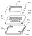
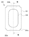
図1は、本形態の半導体装置を構成する支持体を、絶縁性基板の絶縁層ごとに分解して示す斜視図である。図2は、支持体として個片化する前の集合基板の状態を示す上面図である。図3は、本形態の半導体装置の上面図であり、図4は、その背面図である。また、図5および図6は、本形態の半導体装置をそれぞれ別の方向から見た側面図である。さらに、図7は、図3に示すVII−VII方向における半導体装置の断面図である。なお、図1、図4、図5および図6において、鍍金配線および導体配線を網目状の部分で示す。
本形態における半導体装置の製造方法は、絶縁性基板に導体配線が施された支持体を備えた半導体装置の製造方法にかかるものである。特に、支持体を形成する工程が、少なくとも以下に説明する工程1から工程4を有する。
200・・・集合基板
101・・・支持体
101a、101b、101c・・・絶縁層
104・・・凹部
201・・・第一の貫通孔
201a・・・絶縁層101aの角部
201b・・・絶縁層101bの角部
201c・・・絶縁層101cの角部
202・・・第二の貫通孔
202a、202b・・・第二の角部
203・・・半導体素子の搭載部
204・・・導体配線
301a、301b・・・縦方向の分割線
302a、302b・・・横方向の分割線
401・・・半導体素子
402・・・導電性ワイア
403・・・封止部材
404・・・反射部
Claims (3)
- 少なくとも第一のグリーンシートと第二のグリーンシートと第三のグリーンシートとからなる支持体を構成する絶縁性基板を製造する方法であって、
第一のグリーンシートに支持体の凹部の側壁となる貫通孔を形成する工程と、
第二のグリーンシートに半導体素子の搭載部を形成する工程と、
第三のグリーンシートに、第二のグリーンシートとともに支持体の第二の角部を形成するための貫通孔を形成する工程と、
第一のグリーンシートの貫通孔内面に、導電性材料を塗布する工程と、
第二のグリーンシートの上面に、半導体素子に接続する導体配線に対応したパターン形状に、導電性材料を印刷することで、第三の鍍金配線を形成する工程と、
第二のグリーンシートの上面から背面に至る厚さ方向に、第一の貫通孔を形成し、第一の貫通孔に導電性材料を充填することで導体配線を形成して、第二のグリーンシートの上面及び背面に塗布された導電性材料と接続させることで、第一の鍍金配線を形成する工程と、
第三のグリーンシートに、上面方向から見て二つの第一の貫通孔に挟まれた箇所に、第二の貫通孔を形成し、第二の貫通孔に導電性材料を充填して、第三のグリーンシートの上面に塗布された導電性材料と接続させることで、第二の鍍金配線を形成する工程と、
第一乃至第三のグリーンシートとを積み重ねて集合基板を形成することで、第一乃至第三の鍍金配線を、各グリーンシートに形成された導体配線により電気的に接続する工程と、
集合基板を電解液に浸漬した後、第一または第二の鍍金配線に通電することにより、電解鍍金を行う工程と、からなる絶縁性基板の製造方法。 - 集合基板を、第一の貫通孔の中心を結ぶ分割線と、第一の貫通孔と第二の貫通孔の長軸を通る分割線とに沿って分割することで支持体を形成する工程を含む請求項1に記載の絶縁性基板の製造方法。
- 第二の貫通孔は、第一の貫通孔よりも、分割線に沿った方向の内径が大きい請求項2に記載の絶縁性基板の製造方法。
Priority Applications (1)
| Application Number | Priority Date | Filing Date | Title |
|---|---|---|---|
| JP2008158774A JP5359045B2 (ja) | 2008-06-18 | 2008-06-18 | 半導体装置およびその製造方法 |
Applications Claiming Priority (1)
| Application Number | Priority Date | Filing Date | Title |
|---|---|---|---|
| JP2008158774A JP5359045B2 (ja) | 2008-06-18 | 2008-06-18 | 半導体装置およびその製造方法 |
Publications (3)
| Publication Number | Publication Date |
|---|---|
| JP2010003722A JP2010003722A (ja) | 2010-01-07 |
| JP2010003722A5 JP2010003722A5 (ja) | 2011-07-28 |
| JP5359045B2 true JP5359045B2 (ja) | 2013-12-04 |
Family
ID=41585228
Family Applications (1)
| Application Number | Title | Priority Date | Filing Date |
|---|---|---|---|
| JP2008158774A Active JP5359045B2 (ja) | 2008-06-18 | 2008-06-18 | 半導体装置およびその製造方法 |
Country Status (1)
| Country | Link |
|---|---|
| JP (1) | JP5359045B2 (ja) |
Families Citing this family (3)
| Publication number | Priority date | Publication date | Assignee | Title |
|---|---|---|---|---|
| JP5537385B2 (ja) * | 2010-11-04 | 2014-07-02 | スタンレー電気株式会社 | サイドビュー型半導体発光装置およびその製造方法 |
| JP6176302B2 (ja) * | 2015-01-30 | 2017-08-09 | 日亜化学工業株式会社 | 発光装置の製造方法 |
| US9755105B2 (en) | 2015-01-30 | 2017-09-05 | Nichia Corporation | Method for producing light emitting device |
Family Cites Families (5)
| Publication number | Priority date | Publication date | Assignee | Title |
|---|---|---|---|---|
| JP3475757B2 (ja) * | 1997-12-01 | 2003-12-08 | 松下電器産業株式会社 | 面実装型光電変換装置作製用基板 |
| US7244965B2 (en) * | 2002-09-04 | 2007-07-17 | Cree Inc, | Power surface mount light emitting die package |
| JP5073946B2 (ja) * | 2005-12-27 | 2012-11-14 | 新光電気工業株式会社 | 半導体装置および半導体装置の製造方法 |
| JP2007235003A (ja) * | 2006-03-03 | 2007-09-13 | Ngk Spark Plug Co Ltd | 発光素子収納用パッケージ |
| JP5103805B2 (ja) * | 2006-06-27 | 2012-12-19 | 日亜化学工業株式会社 | 発光装置及びその製造方法 |
-
2008
- 2008-06-18 JP JP2008158774A patent/JP5359045B2/ja active Active
Also Published As
| Publication number | Publication date |
|---|---|
| JP2010003722A (ja) | 2010-01-07 |
Similar Documents
| Publication | Publication Date | Title |
|---|---|---|
| RU2690165C2 (ru) | Светоизлучающее устройство | |
| JP5482098B2 (ja) | 発光装置 | |
| JP6747799B2 (ja) | 光素子搭載用パッケージ、光素子搭載用母基板および電子装置 | |
| JP2004253404A (ja) | 発光素子収納用パッケージおよび発光装置 | |
| JP2017117880A (ja) | 光素子搭載用パッケージ、光素子搭載用母基板および電子装置 | |
| JP2008198782A (ja) | 発光装置 | |
| JP4072084B2 (ja) | 発光素子収納用パッケージおよび発光装置 | |
| JP5708766B2 (ja) | 発光装置 | |
| JP4369738B2 (ja) | 発光素子収納用パッケージおよび発光装置 | |
| JP2004319939A (ja) | 発光素子収納用パッケージおよび発光装置 | |
| JP2004281994A (ja) | 発光素子収納用パッケージおよび発光装置 | |
| JP4387160B2 (ja) | 発光素子収納用パッケージの製造方法 | |
| JP5359045B2 (ja) | 半導体装置およびその製造方法 | |
| JP2007258619A (ja) | 発光素子収納用パッケージ | |
| JP2005191111A (ja) | 発光素子収納用パッケージおよび発光装置 | |
| JP4940669B2 (ja) | 半導体素子搭載用の支持体 | |
| JP4164006B2 (ja) | 発光素子収納用パッケージおよび発光装置 | |
| JP2005019688A (ja) | 発光素子収納用パッケージおよび発光装置 | |
| JP4129169B2 (ja) | 発光素子収納用パッケージおよび発光装置 | |
| JP2007273852A (ja) | 発光素子収納用パッケージ | |
| JP4336136B2 (ja) | 発光素子収納用パッケージおよび発光装置 | |
| JP4129173B2 (ja) | 発光素子収納用パッケージおよび発光装置 | |
| JP4132039B2 (ja) | 発光素子収納用パッケージおよび発光装置 | |
| JP2005159082A (ja) | 発光素子収納用パッケージおよび発光装置ならびに発光素子収納用パッケージの製造方法。 | |
| JP2010073734A (ja) | 半導体装置 |
Legal Events
| Date | Code | Title | Description |
|---|---|---|---|
| A521 | Request for written amendment filed |
Free format text: JAPANESE INTERMEDIATE CODE: A523 Effective date: 20110614 |
|
| A621 | Written request for application examination |
Free format text: JAPANESE INTERMEDIATE CODE: A621 Effective date: 20110614 |
|
| A977 | Report on retrieval |
Free format text: JAPANESE INTERMEDIATE CODE: A971007 Effective date: 20120718 |
|
| A131 | Notification of reasons for refusal |
Free format text: JAPANESE INTERMEDIATE CODE: A131 Effective date: 20120821 |
|
| A521 | Request for written amendment filed |
Free format text: JAPANESE INTERMEDIATE CODE: A523 Effective date: 20120913 |
|
| A131 | Notification of reasons for refusal |
Free format text: JAPANESE INTERMEDIATE CODE: A131 Effective date: 20130319 |
|
| A521 | Request for written amendment filed |
Free format text: JAPANESE INTERMEDIATE CODE: A523 Effective date: 20130402 |
|
| TRDD | Decision of grant or rejection written | ||
| A01 | Written decision to grant a patent or to grant a registration (utility model) |
Free format text: JAPANESE INTERMEDIATE CODE: A01 Effective date: 20130806 |
|
| A61 | First payment of annual fees (during grant procedure) |
Free format text: JAPANESE INTERMEDIATE CODE: A61 Effective date: 20130819 |
|
| R150 | Certificate of patent or registration of utility model |
Ref document number: 5359045 Country of ref document: JP Free format text: JAPANESE INTERMEDIATE CODE: R150 Free format text: JAPANESE INTERMEDIATE CODE: R150 |
|
| R250 | Receipt of annual fees |
Free format text: JAPANESE INTERMEDIATE CODE: R250 |
|
| R250 | Receipt of annual fees |
Free format text: JAPANESE INTERMEDIATE CODE: R250 |
|
| R250 | Receipt of annual fees |
Free format text: JAPANESE INTERMEDIATE CODE: R250 |
|
| R250 | Receipt of annual fees |
Free format text: JAPANESE INTERMEDIATE CODE: R250 |
|
| R250 | Receipt of annual fees |
Free format text: JAPANESE INTERMEDIATE CODE: R250 |
|
| R250 | Receipt of annual fees |
Free format text: JAPANESE INTERMEDIATE CODE: R250 |
|
| R250 | Receipt of annual fees |
Free format text: JAPANESE INTERMEDIATE CODE: R250 |