JP5349432B2 - Manufacturing method of electronic component device and resin composition sheet for sealing electronic component used therefor - Google Patents
Manufacturing method of electronic component device and resin composition sheet for sealing electronic component used therefor Download PDFInfo
- Publication number
- JP5349432B2 JP5349432B2 JP2010198623A JP2010198623A JP5349432B2 JP 5349432 B2 JP5349432 B2 JP 5349432B2 JP 2010198623 A JP2010198623 A JP 2010198623A JP 2010198623 A JP2010198623 A JP 2010198623A JP 5349432 B2 JP5349432 B2 JP 5349432B2
- Authority
- JP
- Japan
- Prior art keywords
- sheet
- electronic component
- length
- resin composition
- axis direction
- Prior art date
- Legal status (The legal status is an assumption and is not a legal conclusion. Google has not performed a legal analysis and makes no representation as to the accuracy of the status listed.)
- Expired - Fee Related
Links
Images


Classifications
-
- H—ELECTRICITY
- H01—ELECTRIC ELEMENTS
- H01L—SEMICONDUCTOR DEVICES NOT COVERED BY CLASS H10
- H01L21/00—Processes or apparatus adapted for the manufacture or treatment of semiconductor or solid state devices or of parts thereof
- H01L21/02—Manufacture or treatment of semiconductor devices or of parts thereof
- H01L21/04—Manufacture or treatment of semiconductor devices or of parts thereof the devices having at least one potential-jump barrier or surface barrier, e.g. PN junction, depletion layer or carrier concentration layer
- H01L21/50—Assembly of semiconductor devices using processes or apparatus not provided for in a single one of the subgroups H01L21/06 - H01L21/326, e.g. sealing of a cap to a base of a container
- H01L21/56—Encapsulations, e.g. encapsulation layers, coatings
- H01L21/561—Batch processing
-
- H—ELECTRICITY
- H01—ELECTRIC ELEMENTS
- H01L—SEMICONDUCTOR DEVICES NOT COVERED BY CLASS H10
- H01L21/00—Processes or apparatus adapted for the manufacture or treatment of semiconductor or solid state devices or of parts thereof
- H01L21/02—Manufacture or treatment of semiconductor devices or of parts thereof
- H01L21/04—Manufacture or treatment of semiconductor devices or of parts thereof the devices having at least one potential-jump barrier or surface barrier, e.g. PN junction, depletion layer or carrier concentration layer
- H01L21/50—Assembly of semiconductor devices using processes or apparatus not provided for in a single one of the subgroups H01L21/06 - H01L21/326, e.g. sealing of a cap to a base of a container
- H01L21/56—Encapsulations, e.g. encapsulation layers, coatings
- H01L21/563—Encapsulation of active face of flip-chip device, e.g. underfilling or underencapsulation of flip-chip, encapsulation preform on chip or mounting substrate
-
- H—ELECTRICITY
- H01—ELECTRIC ELEMENTS
- H01L—SEMICONDUCTOR DEVICES NOT COVERED BY CLASS H10
- H01L23/00—Details of semiconductor or other solid state devices
- H01L23/28—Encapsulations, e.g. encapsulating layers, coatings, e.g. for protection
-
- H—ELECTRICITY
- H01—ELECTRIC ELEMENTS
- H01L—SEMICONDUCTOR DEVICES NOT COVERED BY CLASS H10
- H01L23/00—Details of semiconductor or other solid state devices
- H01L23/28—Encapsulations, e.g. encapsulating layers, coatings, e.g. for protection
- H01L23/29—Encapsulations, e.g. encapsulating layers, coatings, e.g. for protection characterised by the material, e.g. carbon
- H01L23/293—Organic, e.g. plastic
- H01L23/295—Organic, e.g. plastic containing a filler
-
- H—ELECTRICITY
- H01—ELECTRIC ELEMENTS
- H01L—SEMICONDUCTOR DEVICES NOT COVERED BY CLASS H10
- H01L23/00—Details of semiconductor or other solid state devices
- H01L23/28—Encapsulations, e.g. encapsulating layers, coatings, e.g. for protection
- H01L23/31—Encapsulations, e.g. encapsulating layers, coatings, e.g. for protection characterised by the arrangement or shape
- H01L23/3107—Encapsulations, e.g. encapsulating layers, coatings, e.g. for protection characterised by the arrangement or shape the device being completely enclosed
- H01L23/3121—Encapsulations, e.g. encapsulating layers, coatings, e.g. for protection characterised by the arrangement or shape the device being completely enclosed a substrate forming part of the encapsulation
-
- H—ELECTRICITY
- H01—ELECTRIC ELEMENTS
- H01L—SEMICONDUCTOR DEVICES NOT COVERED BY CLASS H10
- H01L24/00—Arrangements for connecting or disconnecting semiconductor or solid-state bodies; Methods or apparatus related thereto
- H01L24/74—Apparatus for manufacturing arrangements for connecting or disconnecting semiconductor or solid-state bodies
- H01L24/75—Apparatus for connecting with bump connectors or layer connectors
-
- H—ELECTRICITY
- H01—ELECTRIC ELEMENTS
- H01L—SEMICONDUCTOR DEVICES NOT COVERED BY CLASS H10
- H01L2224/00—Indexing scheme for arrangements for connecting or disconnecting semiconductor or solid-state bodies and methods related thereto as covered by H01L24/00
- H01L2224/73—Means for bonding being of different types provided for in two or more of groups H01L2224/10, H01L2224/18, H01L2224/26, H01L2224/34, H01L2224/42, H01L2224/50, H01L2224/63, H01L2224/71
- H01L2224/732—Location after the connecting process
- H01L2224/73201—Location after the connecting process on the same surface
- H01L2224/73203—Bump and layer connectors
-
- H—ELECTRICITY
- H01—ELECTRIC ELEMENTS
- H01L—SEMICONDUCTOR DEVICES NOT COVERED BY CLASS H10
- H01L2924/00—Indexing scheme for arrangements or methods for connecting or disconnecting semiconductor or solid-state bodies as covered by H01L24/00
- H01L2924/10—Details of semiconductor or other solid state devices to be connected
- H01L2924/102—Material of the semiconductor or solid state bodies
- H01L2924/1025—Semiconducting materials
- H01L2924/10251—Elemental semiconductors, i.e. Group IV
- H01L2924/10253—Silicon [Si]
-
- H—ELECTRICITY
- H01—ELECTRIC ELEMENTS
- H01L—SEMICONDUCTOR DEVICES NOT COVERED BY CLASS H10
- H01L2924/00—Indexing scheme for arrangements or methods for connecting or disconnecting semiconductor or solid-state bodies as covered by H01L24/00
- H01L2924/10—Details of semiconductor or other solid state devices to be connected
- H01L2924/11—Device type
- H01L2924/12—Passive devices, e.g. 2 terminal devices
- H01L2924/1204—Optical Diode
- H01L2924/12042—LASER
-
- Y—GENERAL TAGGING OF NEW TECHNOLOGICAL DEVELOPMENTS; GENERAL TAGGING OF CROSS-SECTIONAL TECHNOLOGIES SPANNING OVER SEVERAL SECTIONS OF THE IPC; TECHNICAL SUBJECTS COVERED BY FORMER USPC CROSS-REFERENCE ART COLLECTIONS [XRACs] AND DIGESTS
- Y10—TECHNICAL SUBJECTS COVERED BY FORMER USPC
- Y10T—TECHNICAL SUBJECTS COVERED BY FORMER US CLASSIFICATION
- Y10T29/00—Metal working
- Y10T29/49—Method of mechanical manufacture
- Y10T29/49002—Electrical device making
- Y10T29/49117—Conductor or circuit manufacturing
- Y10T29/49124—On flat or curved insulated base, e.g., printed circuit, etc.
- Y10T29/4913—Assembling to base an electrical component, e.g., capacitor, etc.
- Y10T29/49146—Assembling to base an electrical component, e.g., capacitor, etc. with encapsulating, e.g., potting, etc.
-
- Y—GENERAL TAGGING OF NEW TECHNOLOGICAL DEVELOPMENTS; GENERAL TAGGING OF CROSS-SECTIONAL TECHNOLOGIES SPANNING OVER SEVERAL SECTIONS OF THE IPC; TECHNICAL SUBJECTS COVERED BY FORMER USPC CROSS-REFERENCE ART COLLECTIONS [XRACs] AND DIGESTS
- Y10—TECHNICAL SUBJECTS COVERED BY FORMER USPC
- Y10T—TECHNICAL SUBJECTS COVERED BY FORMER US CLASSIFICATION
- Y10T428/00—Stock material or miscellaneous articles
- Y10T428/31504—Composite [nonstructural laminate]
Description
本発明は、簡便にオーバーモールドおよびアンダーフィルが可能な電子部品装置の製法およびそれに用いる電子部品封止用樹脂組成物シートに関するものである。 The present invention relates to a method for producing an electronic component device that can be easily overmolded and underfilled, and an electronic component sealing resin composition sheet used therefor.
従来、実装基板上に設置した半導体素子、コンデンサおよび抵抗素子等の電子部品の封止は、粉末状エポキシ樹脂組成物によるトランスファー封止や、液状エポキシ樹脂組成物、シリコーン樹脂等によるポッティング、ディスペンス、印刷等によって行われている。また、近年、より安価で簡便な封止方法として、樹脂組成物シートを用いたシート封止も提案されている(特許文献1〜3参照)。
Conventionally, sealing of electronic components such as semiconductor elements, capacitors, and resistance elements installed on a mounting substrate is performed by transfer sealing with a powdered epoxy resin composition, potting with a liquid epoxy resin composition, silicone resin, etc., dispensing, This is done by printing. In recent years, sheet sealing using a resin composition sheet has also been proposed as a cheaper and simpler sealing method (see
これら樹脂組成物シートを用いた封止では、電子部品上にシート材を設置して加熱プレスすることにより、オーバーモールドおよびアンダーフィルを行う。しかし、封止条件によっては、溶融した樹脂組成物が漏れ出して、実装基板やプレス機等の汚染が生じたり、アンダーフィルの充填不良が起こることがある。このような場合の対処法として、例えば、漏れ出しを防ぐための治具を装着するといったことが行われる。しかしながら、この対処法では、電子部品のサイズや形状により治具を変更する必要があり、生産性に問題があった。 In sealing using these resin composition sheets, overmolding and underfilling are performed by placing a sheet material on an electronic component and heating and pressing. However, depending on the sealing conditions, the molten resin composition may leak out, causing contamination of the mounting substrate, press machine, etc., or underfill filling failure. As a countermeasure for such a case, for example, a jig for preventing leakage is attached. However, in this countermeasure, it is necessary to change the jig depending on the size and shape of the electronic component, and there is a problem in productivity.
本発明は、このような事情に鑑みなされたもので、溶融した樹脂組成物の漏れ出しを防ぐ治具を必要とすることなく、簡便にオーバーモールドおよびアンダーフィルが可能な電子部品装置の製法およびそれに用いる電子部品封止用樹脂組成物シートの提供をその目的とする。 The present invention has been made in view of such circumstances, and without requiring a jig for preventing leakage of a molten resin composition, a method for producing an electronic component device capable of easily overmolding and underfilling, and An object of the present invention is to provide a resin composition sheet for encapsulating electronic components used therefor.
上記の問題を解決するために、本発明は、実装基板上に複数の電子部品を並べて設置した後、上記実装基板における電子部品搭載エリア上に、下記(B)に示す熱硬化性樹脂組成物シート〔シートB〕、およびその上に下記(A)に示す熱硬化性樹脂組成物シート〔シートA〕を積載し、かつ上記電子部品搭載エリアの中心および平面XY方向と、両シートA,Bの中心および平面XY方向とが略合致するよう設置する工程と、この設置状態を保持した上記実装基板を、減圧状態のチャンバー内で70〜150℃から選ばれる成形温度に加熱し、上記シートAの全周の端部を軟化により実装基板に接するまで垂れ下がらせ、シートAの全周で囲われた空間を密閉する工程と、この垂れ下がり状態においてシートBおよび電子部品を被覆した上記シートAをプレスする工程と、上記チャンバー内の圧力を開放し、上記シートAと実装基板との間に形成された密閉空間内で、シートBの溶融物による電子部品のアンダーフィルを行う工程と、上記アンダーフィルを行った後、両シートA,Bの樹脂組成物を熱硬化させ、実装基板上の複数の電子部品が樹脂封止されてなる電子部品装置集合体を得る工程と、この電子部品装置集合体をダイシングし、個々の電子部品装置を得る工程とを備えた電子部品装置の製法を第1の要旨とする。
(A)上記成形温度における粘度が2000〜50000Pa・sであり、かつ、その寸法が下記の条件(1)を満たす熱硬化性樹脂組成物シート。
<条件(1)>
Ax>P+8
Ay>Q+8
〔Ax:シートAのX軸方向長さ(mm),Ay:シートAのY軸方向長さ(mm),P:電子部品搭載エリアのX方向の長さ(mm),Q:電子部品搭載エリアのY方向の長さ(mm)〕
(B)上記成形温度における粘度が20〜250Pa・sであり、かつ、その寸法が下記の条件(2)を満たす熱硬化性樹脂組成物シート。
<条件(2)>
Ax≧Bx>P×0.8
Ay≧By>Q×0.8
〔Bx:シートBのX軸方向長さ(mm),By:シートBのY軸方向長さ(mm),P:電子部品搭載エリアのX方向の長さ(mm),Q:電子部品搭載エリアのY方向の長さ(mm),Ax:シートAのX軸方向長さ(mm),Ay:シートAのY軸方向長さ(mm)〕
In order to solve the above problem, the present invention provides a thermosetting resin composition shown in (B) below on an electronic component mounting area of the mounting substrate after a plurality of electronic components are arranged side by side on the mounting substrate. A sheet [Sheet B] and a thermosetting resin composition sheet [Sheet A] shown below (A) are stacked thereon, and the center of the electronic component mounting area and the plane XY direction, and both sheets A and B The sheet A is heated to a molding temperature selected from 70 to 150 ° C. in a reduced-pressure chamber in a step of installing so that the center of the substrate and the plane XY direction substantially match each other, and the mounting substrate maintaining this installation state. The step of hanging the end of the entire circumference of the sheet A until it comes into contact with the mounting substrate by softening, sealing the space enclosed by the entire circumference of the sheet A, and covering the sheet B and the electronic component in the suspended state A step of pressing the sheet A, a step of releasing the pressure in the chamber, and underfilling the electronic component with a melt of the sheet B in a sealed space formed between the sheet A and the mounting substrate; After the underfill is performed, the resin composition of both sheets A and B is thermally cured to obtain an electronic component device assembly in which a plurality of electronic components on the mounting substrate are sealed with resin. A first gist is a method of manufacturing an electronic component device including a step of dicing a component device assembly to obtain individual electronic component devices.
(A) A thermosetting resin composition sheet having a viscosity of 2000 to 50000 Pa · s at the molding temperature and satisfying the following condition (1).
<Condition (1)>
Ax> P + 8
Ay> Q + 8
[Ax: Length of the sheet A in the X-axis direction (mm), Ay: Length of the sheet A in the Y-axis direction (mm), P: Length of the electronic component mounting area in the X direction (mm), Q: Electronic component mounting Area length in Y direction (mm)]
(B) A thermosetting resin composition sheet having a viscosity at the molding temperature of 20 to 250 Pa · s and a dimension satisfying the following condition (2).
<Condition (2)>
Ax ≧ Bx> P × 0.8
Ay ≧ By> Q × 0.8
[Bx: Length of the sheet B in the X-axis direction (mm), By: Length of the sheet B in the Y-axis direction (mm), P: Length of the electronic component mounting area in the X direction (mm), Q: Electronic component mounting Length of area in Y direction (mm), Ax: Length of sheet A in X axis direction (mm), Ay: Length of sheet A in Y axis direction (mm)]
また、本発明は、上記第1の要旨の製法に用いられる樹脂組成物シートであって、上記シートAとシートBとからなるシートセットである電子部品封止用樹脂組成物シートを第2の要旨とし、上記シートAとシートBとが積層一体化されてなる電子部品封止用樹脂組成物シートを第3の要旨とする。 In addition, the present invention provides a resin composition sheet used in the production method of the first aspect, wherein the second resin composition sheet for sealing an electronic component, which is a sheet set comprising the sheet A and the sheet B, is used. A third gist is a resin composition sheet for sealing an electronic component in which the sheet A and the sheet B are laminated and integrated.
すなわち、本発明者らは、前記課題を解決するため鋭意研究を重ねた。その結果、上記のように、電子部品封止用の熱硬化性樹脂組成物シートとして、70〜150℃から選ばれる成形温度(加熱温度)において、その粘度、および寸法が、互いに異なる二枚のシートA,B(もしくは、シートA,Bが積層一体化されたもの)を用いることを想起した。すなわち、実装基板上の電子部品搭載エリアに合わせ、上記エリアよりもやや小さいか、若干大きいシートBを積載し、さらにその上に、上記エリアよりも大きいシートAを積載し、減圧状態のチャンバー内で上記成形温度に加熱すると、シートAの全周の端部が軟化により実装基板に接するまで垂れ下がって、シートAがシートBおよび電子部品を被覆した状態となる(図3(iv)参照)。このとき、上記シートAは、その被覆により、実装基板との間に密閉空間を形成し、その密閉空間内で、シートBは低粘度のゲル状となっている。この状態で、上記シートAの上からプレス板でプレスし、さらにチャンバー内の圧力を開放すると、上記密閉空間内で、シートBが溶融物となって、実装基板と電子部品のギャップに入り込み、電子部品のアンダーフィルがなされるようになる。また、シートAは、上記被覆により、シートBの溶融物の漏れ出しを防ぐ治具の役割を果たしつつ、オーバーモールドとしての役割も果たす。これにより、樹脂組成物の漏れ出しを防ぐ治具を必要とすることなく、簡便にオーバーモールドおよびアンダーフィルが達成できることを見いだし、本発明に到達した。 That is, the present inventors have intensively studied to solve the above problems. As a result, as described above, as a thermosetting resin composition sheet for sealing electronic components, at a molding temperature (heating temperature) selected from 70 to 150 ° C., two viscosities and dimensions differ from each other. It was recalled that sheets A and B (or sheets A and B were laminated and integrated) were used. That is, in accordance with the electronic component mounting area on the mounting substrate, a sheet B slightly smaller than or slightly larger than the above area is stacked, and further, a sheet A larger than the above area is stacked thereon, When the sheet is heated to the above molding temperature, the end of the entire circumference of the sheet A hangs down until it comes into contact with the mounting substrate due to softening, so that the sheet A covers the sheet B and the electronic component (see FIG. 3 (iv)). At this time, the sheet A forms a sealed space with the mounting substrate by the coating, and the sheet B is in a low-viscosity gel form in the sealed space. In this state, pressing with a press plate from above the sheet A, and further releasing the pressure in the chamber, in the sealed space, the sheet B becomes a melt, and enters the gap between the mounting substrate and the electronic component, Underfill of electronic parts will be made. The sheet A also serves as an overmold while serving as a jig that prevents the melt of the sheet B from leaking out due to the coating. Thereby, it was found that overmolding and underfilling can be easily achieved without requiring a jig for preventing leakage of the resin composition, and the present invention has been achieved.
以上のように、本発明の電子部品装置の製法は、実装基板上の電子部品搭載エリアに合わせ、上記エリアよりもやや小さいか、若干大きい、成形温度(70〜150℃から選ばれる温度)における粘度が20〜250Pa・sのシートBを積載し、さらにその上に、上記エリアよりも大きく、上記成形温度における粘度が2000〜50000Pa・sのシートAを積載した後、減圧状態のチャンバー内で上記成形温度に加熱し、上記シートAがシートBおよび電子部品を被覆した状態となるまで垂れ下がらせ、その後、上記チャンバー内の圧力を開放し、上記シートAの被覆により実装基板との間に形成された密閉空間内で、シートBの溶融物による電子部品のアンダーフィルを行っている。そのため、樹脂組成物の漏れ出しを防ぐ治具を使用しなくとも、簡便にオーバーモールドおよびアンダーフィルを達成することができる。これにより、溶融した樹脂組成物の漏れ出しによる実装基板やプレス機等の汚染や、アンダーフィルの充填性不良を解消することができる。 As described above, the manufacturing method of the electronic component device according to the present invention is at a molding temperature (a temperature selected from 70 to 150 ° C.) that is slightly smaller or slightly larger than the area according to the electronic component mounting area on the mounting substrate. A sheet B having a viscosity of 20 to 250 Pa · s is stacked, and a sheet A having a viscosity larger than that of the area and having a viscosity of 2000 to 50000 Pa · s at the molding temperature is further stacked on the sheet B. Heat to the molding temperature and let the sheet A hang down until it is in a state of covering the sheet B and the electronic components, then release the pressure in the chamber and cover the mounting substrate with the sheet A. Underfilling of the electronic component with the melt of the sheet B is performed in the formed sealed space. Therefore, overmolding and underfilling can be easily achieved without using a jig for preventing leakage of the resin composition. As a result, it is possible to eliminate the contamination of the mounting substrate and the press machine due to the leakage of the molten resin composition and the underfill filling failure.
そして、電子部品封止用樹脂組成物シートが、上記シートAとシートBとが積層一体化されてなるものであると、取り扱い等の観点から、上記製法において、より好ましく用いることができる。 And it can use more preferably in the said manufacturing method from viewpoints of handling that the resin composition sheet | seat for electronic component sealing is what the said sheet | seat A and the sheet | seat B are laminated and integrated.
つぎに、本発明の実施の形態について詳しく説明する。 Next, embodiments of the present invention will be described in detail.
本発明の電子部品装置の製法は、先に述べたように、実装基板上に複数の電子部品を並べて設置した後、上記実装基板における電子部品搭載エリア上に、シートB、およびその上にシートAを積載し、かつ上記電子部品搭載エリアの中心および平面XY方向と、両シートA,Bの中心および平面XY方向とが略合致するよう設置する工程と、この設置状態を保持した上記実装基板を、減圧状態のチャンバー内で70〜150℃から選ばれる成形温度に加熱し、上記シートAの全周の端部を軟化により実装基板に接するまで垂れ下がらせ、シートAの全周で囲われた空間を密閉する工程と、この垂れ下がり状態においてシートBおよび電子部品を被覆した上記シートAをプレスする工程と、上記チャンバー内の圧力を開放し、上記シートAと実装基板との間に形成された密閉空間内で、シートBの溶融物による電子部品のアンダーフィルを行う工程と、上記アンダーフィルを行った後、両シートA,Bの樹脂組成物を熱硬化させ、実装基板上の複数の電子部品が樹脂封止されてなる電子部品装置集合体を得る工程と、この電子部品装置集合体をダイシングし、個々の電子部品装置を得る工程とを備えている。なお、上記電子部品搭載エリアの平面XY方向とは、電子部品搭載エリア平面上で任意に決められるX方向と、上記平面上でこれに直行するY方向とを示すものである。両シートA,Bの平面XY方向も、同様の趣旨である。また、「上記電子部品搭載エリアの中心および平面XY方向と、両シートA,Bの中心および平面XY方向とが略合致するよう設置」と規定されていることから、本発明はこの設置に関し、中心および平面XY方向の若干のずれも含める趣旨である。 As described above, according to the method of manufacturing the electronic component device of the present invention, after arranging a plurality of electronic components on the mounting board, the sheet B is placed on the electronic component mounting area of the mounting board, and the sheet is placed thereon. A mounting process in which the center of the electronic component mounting area and the plane XY direction and the center of both sheets A and B and the plane XY direction substantially coincide with each other, and the mounting substrate that maintains this installation state Is heated to a molding temperature selected from 70 to 150 ° C. in a reduced-pressure chamber, and the end of the entire circumference of the sheet A is allowed to hang down until it comes into contact with the mounting board by softening, and is surrounded by the entire circumference of the sheet A. A step of sealing the closed space, a step of pressing the sheet A covered with the sheet B and the electronic component in the hanging state, a pressure in the chamber is released, and In the sealed space formed between the substrate and the underfill of the electronic component by the melt of the sheet B, and after the underfill, the resin compositions of both sheets A and B are thermally cured. And a step of obtaining an electronic component device assembly in which a plurality of electronic components on the mounting substrate are sealed with resin, and a step of dicing the electronic component device assembly to obtain individual electronic component devices. The plane XY direction of the electronic component mounting area indicates an X direction arbitrarily determined on the electronic component mounting area plane and a Y direction orthogonal to the plane on the plane. The plane XY directions of both sheets A and B have the same purpose. In addition, since it is defined as “installation so that the center and plane XY direction of the electronic component mounting area and the center and plane XY direction of both sheets A and B substantially match”, the present invention relates to this installation. It is intended to include a slight shift in the center and plane XY directions.
そして、上記シートAとしては、先述のようにして選ばれた成形温度(70〜150℃)における粘度が、2000〜50000Pa・sであり、かつ、その寸法が下記の条件(1)を満たす熱硬化性樹脂組成物シートが用いられる。上記寸法条件は、生産性よく封止できるという観点から、好ましくは、下記の条件(1′)である。すなわち、このような特定の粘度およびサイズを有するシートAを、先に述べた本発明の電子部品装置の製法に示すように用いると、シートAが上記のように垂れ下がってシートBの溶融物の漏れ出しを防ぐ機能を果たし、それにより、漏れ出しを防ぐ治具を必要とすることなく、電子部品の封止が可能となる。なお、上記シートAの、上記成形温度における粘度が、2000Pa・s未満であると、シートA自体が溶融して樹脂漏れを起こすおそれがあり、50000Pa・sを超えると、シートBの溶融物の漏れ出しを防ぐ治具としての機能の果たせず、アンダーフィル充填不良の傾向がみられる。そのため、上記のように粘度を規定している。また、上記温度条件における粘度は、一般的なレオメーターを用いて測定すればよいが、例えば、回転型粘度計(HAKKE社製、レオストレスRS1)を用い、ギャップ100μm、回転コーン直径20mm、回転速度10s-1という条件で測定することにより導き出すことができる。 And as said sheet A, the viscosity in the molding temperature (70-150 degreeC) selected as mentioned above is 2000-50000 Pa.s, and the dimension satisfy | fills the following conditions (1). A curable resin composition sheet is used. The above dimensional condition is preferably the following condition (1 ′) from the viewpoint that sealing can be performed with high productivity. That is, when the sheet A having such a specific viscosity and size is used as shown in the above-described manufacturing method of the electronic component device of the present invention, the sheet A hangs down as described above and the melt of the sheet B The electronic component can be sealed without requiring a jig for preventing leakage, thereby preventing leakage. In addition, when the viscosity at the molding temperature of the sheet A is less than 2000 Pa · s, the sheet A itself may be melted to cause resin leakage. When the viscosity exceeds 50000 Pa · s, the melt of the sheet B It does not function as a jig to prevent leakage, and there is a tendency for poor underfill filling. Therefore, the viscosity is specified as described above. The viscosity under the above temperature conditions may be measured using a general rheometer. For example, using a rotary viscometer (manufactured by HAKKE, rheostress RS1), the gap is 100 μm, the rotating cone diameter is 20 mm, the rotating It can be derived by measuring at a speed of 10 s −1 .
<条件(1)>
Ax>P+8
Ay>Q+8
〔Ax:シートAのX軸方向長さ(mm),Ay:シートAのY軸方向長さ(mm),P:電子部品搭載エリアのX方向の長さ(mm),Q:電子部品搭載エリアのY方向の長さ(mm)〕
<Condition (1)>
Ax> P + 8
Ay> Q + 8
[Ax: Length of the sheet A in the X-axis direction (mm), Ay: Length of the sheet A in the Y-axis direction (mm), P: Length of the electronic component mounting area in the X direction (mm), Q: Electronic component mounting Area length in Y direction (mm)]
<条件(1′)>
t1+t2+40+P>Ax>t1+t2+8+P
t1+t2+40+Q>Ay>t1+t2+8+Q
(t1+0.5)−〔(n×Vc)/(P×Q)〕>Az>t1−〔(n×Vc)/(P×Q)〕
〔Ax:シートAのX軸方向長さ(mm),Ay:シートAのY軸方向長さ(mm),Az:シートAの厚み(mm),t1:電子部品の厚み(mm),t2:電子部品の接続用電極部高さ(mm),P:電子部品搭載エリアのX方向の長さ(mm),Q:電子部品搭載エリアのY方向の長さ(mm),Vc:電子部品1個あたりの体積(mm3),n:封止する電子部品の個数〕
<Condition (1 ')>
t1 + t2 + 40 + P>Ax> t1 + t2 + 8 + P
t1 + t2 + 40 + Q>Ay> t1 + t2 + 8 + Q
(T1 + 0.5)-[(n * Vc) / (P * Q)]>Az> t1-[(n * Vc) / (P * Q)]
[Ax: length of the sheet A in the X-axis direction (mm), Ay: length of the sheet A in the Y-axis direction (mm), Az: thickness of the sheet A (mm), t1: thickness of the electronic component (mm), t2 : Height of electrode part for connection of electronic component (mm), P: length of electronic component mounting area in X direction (mm), Q: length of electronic component mounting area in Y direction (mm), Vc: electronic component Volume per unit (mm 3 ), n: number of electronic components to be sealed]
また、上記シートBとしては、先述のようにして選ばれた成形温度(70〜150℃)における粘度が、20〜250Pa・sであり、かつ、その寸法が下記の条件(2)を満たす熱硬化性樹脂組成物シートが用いられる。上記寸法条件は、生産性よく封止できるという観点から、好ましくは、下記の条件(2′)である。すなわち、このような特定の粘度およびサイズを有するシートBを、先に述べた本発明の電子部品装置の製法に示すように用いると、実装基板と電子部品の狭ギャップにもシートBの溶融物が入り込み、アンダーフィルが容易となる。なお、上記シートBの、上記成形温度における粘度が、20Pa・s未満であると、シートBがタック性を有するようになるため取扱いが困難になる傾向がみられ、250Pa・sを超えると、アンダーフィル充填が因難となる傾向がみられる。そのため、上記のように粘度を規定している。また、上記温度条件における粘度は、シートAのときと同様にして測定することにより導き出すことができる。 Further, the sheet B has a viscosity at a molding temperature (70 to 150 ° C.) selected as described above of 20 to 250 Pa · s, and its dimensions satisfy the following condition (2). A curable resin composition sheet is used. The above dimensional condition is preferably the following condition (2 ′) from the viewpoint that sealing can be performed with high productivity. That is, when the sheet B having such a specific viscosity and size is used as shown in the above-described manufacturing method of the electronic component device of the present invention, the melt of the sheet B is also applied to the narrow gap between the mounting substrate and the electronic component. Enters and facilitates underfill. In addition, when the viscosity at the molding temperature of the sheet B is less than 20 Pa · s, the sheet B tends to be difficult to handle because it has tackiness, and when it exceeds 250 Pa · s, There is a tendency to underfill filling. Therefore, the viscosity is specified as described above. Moreover, the viscosity in the said temperature conditions can be derived by measuring similarly to the case of the sheet | seat A. FIG.
<条件(2)>
Ax≧Bx>P×0.8
Ay≧By>Q×0.8
〔Bx:シートBのX軸方向長さ(mm),By:シートBのY軸方向長さ(mm),P:電子部品搭載エリアのX方向の長さ(mm),Q:電子部品搭載エリアのY方向の長さ(mm),Ax:シートAのX軸方向長さ(mm),Ay:シートAのY軸方向長さ(mm)〕
<Condition (2)>
Ax ≧ Bx> P × 0.8
Ay ≧ By> Q × 0.8
[Bx: Length of the sheet B in the X-axis direction (mm), By: Length of the sheet B in the Y-axis direction (mm), P: Length of the electronic component mounting area in the X direction (mm), Q: Electronic component mounting Length of area in Y direction (mm), Ax: Length of sheet A in X axis direction (mm), Ay: Length of sheet A in Y axis direction (mm)]
<条件(2′)>
Ax≧Bx>P×0.8
Ay≧By>Q×0.8
{〔P×Q×(t1+t2)−n(Vc+Vb)〕/(P×Q)}+0.1>Bz>(t2×P×Q−Vb×n)/(P×Q)
〔Bx:シートBのX軸方向長さ(mm),By:シートBのY軸方向長さ(mm),Bz:シートBの厚み(mm),t1:電子部品の厚み(mm),t2:電子部品の接続用電極部高さ(mm),P:電子部品搭載エリアのX方向の長さ(mm),Q:電子部品搭載エリアのY方向の長さ(mm),Vb:電子部品1個に搭載されているバンプ(接続用電極部)の総体積(mm3),Vc:チップ1個あたりの体積(mm3),n:封止する電子部品の個数),Ax:シートAのX軸方向長さ(mm),Ay:シートAのY軸方向長さ(mm)〕
<Condition (2 ')>
Ax ≧ Bx> P × 0.8
Ay ≧ By> Q × 0.8
{[P * Q * (t1 + t2) -n (Vc + Vb)] / (P * Q)} + 0.1>Bz> (t2 * P * Q-Vb * n) / (P * Q)
[Bx: length of the sheet B in the X-axis direction (mm), By: length of the sheet B in the Y-axis direction (mm), Bz: thickness of the sheet B (mm), t1: thickness of the electronic component (mm), t2 : Height of connecting electrode part (mm) for electronic component, P: length of electronic component mounting area in X direction (mm), Q: length of electronic component mounting area in Y direction (mm), Vb: electronic component Total volume (mm 3 ) of bumps (electrodes for connection) mounted on one, Vc: Volume per chip (mm 3 ), n: Number of electronic components to be sealed, Ax: Sheet A X-axis direction length (mm), Ay: Y-axis direction length of sheet A (mm)]
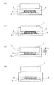
ここで、図1は、上記条件(1)〜(2′)において長さ等が規定された箇所を具体的に示すための説明図であり、(i)はシートAの斜視図、(ii)はシートBの斜視図、(iii)は電子部品の側面図、(iv)はn個の電子部品を並べて設置した実装基板の平面図である。なお、図における各符号は、上記条件(1)〜(2′)の記載に対応している。また、図において、3は実装基板、5は電子部品、6は電子部品の接続用電極部(バンプ)、7はシートA、8はシートBを示す。 Here, FIG. 1 is an explanatory view for specifically showing a portion where the length or the like is defined in the above conditions (1) to (2 ′), (i) is a perspective view of the sheet A, and (ii) ) Is a perspective view of the sheet B, (iii) is a side view of the electronic component, and (iv) is a plan view of a mounting substrate in which n electronic components are arranged side by side. In addition, each code | symbol in a figure respond | corresponds to description of the said conditions (1)-(2 '). In the figure, 3 is a mounting substrate, 5 is an electronic component, 6 is an electrode part (bump) for connection of the electronic component, 7 is a sheet A, and 8 is a sheet B.
ところで、上記シートAは、先に述べたように、70〜150℃から選ばれる成形温度
における粘度が特定の範囲であり、かつそのサイズが特定の条件を満たす熱硬化性樹脂組成物シートであれば、その材料は、特に限定はないが、好ましくは、下記(a)〜(d)成分を含有するエポキシ樹脂組成物が用いられる。
(a)25℃における粘度が1.0〜10.0Pa・sであるエポキシ樹脂。
(b)硬化剤。
(c)下記の(c1)〜(c3)成分からなり、(c2)および(c3)成分の合計含有量が、(c1)成分100重量部に対して2〜60重量部の範囲内である無機質充填剤。
(c1)平均粒径が5〜20μmの無機質充填剤。
(c2)平均粒径が1〜3μmの無機質充填剤。
(c3)平均粒径が0.3〜0.8μmの無機質充填剤。
(d)可撓性付与剤。
By the way, as described above, the sheet A is a thermosetting resin composition sheet whose viscosity at a molding temperature selected from 70 to 150 ° C. is in a specific range and whose size satisfies a specific condition. For example, the material is not particularly limited, but an epoxy resin composition containing the following components (a) to (d) is preferably used.
(A) An epoxy resin having a viscosity at 25 ° C. of 1.0 to 10.0 Pa · s.
(B) Curing agent.
(C) It consists of the following components (c1) to (c3), and the total content of components (c2) and (c3) is in the range of 2 to 60 parts by weight with respect to 100 parts by weight of component (c1). Inorganic filler.
(C1) An inorganic filler having an average particle diameter of 5 to 20 μm.
(C2) An inorganic filler having an average particle diameter of 1 to 3 μm.
(C3) An inorganic filler having an average particle size of 0.3 to 0.8 μm.
(D) Flexibility imparting agent.
上記(a)成分のエポキシ樹脂としては、25℃における粘度が1.0〜10.0Pa・sである、ビスフェノールA型エポキシ樹脂,ビスフェノールF型エポキシ樹脂,グリシジルアミン型エポキシ樹脂,グリシジルエステル型エポキシ樹脂等があげられる。なかでも、樹脂組成物の硬化性の観点から、上記粘度を有する、ビスフェノールA型エポキシ樹脂,ビスフェノールF型エポキシ樹脂が好ましい。なお、市販品では、EXA−850CRP(DIC社製)、EPON−827、YL−983U(以上、三菱化学社製)等が、上記(a)成分のエポキシ樹脂として入手可能である。また、上記(a)成分のエポキシ樹脂の粘度は、一般的なレオメーターを用いて測定すればよいが、例えば、回転型粘度計(HAKKE社製、レオストレスRS1)を用い、ギャップ100μm、回転コーン直径20mm、回転速度10s-1という条件で測定することにより導き出すことができる。 As the epoxy resin of component (a), the viscosity at 25 ° C. is 1.0 to 10.0 Pa · s, bisphenol A type epoxy resin, bisphenol F type epoxy resin, glycidylamine type epoxy resin, glycidyl ester type epoxy. Examples thereof include resins. Especially, the bisphenol A type epoxy resin and the bisphenol F type epoxy resin which have the said viscosity from a sclerosing | hardenable viewpoint of a resin composition are preferable. As commercial products, EXA-850CRP (manufactured by DIC), EPON-827, YL-983U (manufactured by Mitsubishi Chemical Co., Ltd.) and the like are available as the epoxy resin of the component (a). The viscosity of the epoxy resin as component (a) may be measured using a general rheometer. For example, a rotational viscometer (manufactured by HAKKE, rheostress RS1) is used, and a gap of 100 μm is rotated. It can be derived by measuring under conditions of a cone diameter of 20 mm and a rotational speed of 10 s −1 .
上記シートAを構成するエポキシ樹脂組成物中の(a)成分の含有量は、シートAの粘度調整およびその樹脂組成物硬化体の信頼性の観点から、上記樹脂組成物の8〜17重量%が好ましく、より好ましくは9〜12重量%である。 The content of the component (a) in the epoxy resin composition constituting the sheet A is 8 to 17% by weight of the resin composition from the viewpoint of adjusting the viscosity of the sheet A and the reliability of the cured resin composition. Is more preferable, and more preferably 9 to 12% by weight.
なお、(a)成分以外のエポキシ樹脂を併用する場合は、(a)成分が全エポキシ樹脂の80重量%以上となるようにすることが好ましい。 In addition, when using together epoxy resins other than (a) component, it is preferable that (a) component shall be 80 weight% or more of all the epoxy resins.
上記(b)成分の硬化剤には、(a)成分のエポキシ樹脂と硬化反応を生起する成分が用いられる。このような硬化剤としては、例えば、フェノール樹脂、酸無水物、アミン化合物があげられる。なかでも、(a)成分との反応性の観点から、フェノール樹脂が好ましく、シートAの粘度調整の観点から、軟化点が60〜130℃のフェノール樹脂がより好ましく、樹脂組成物硬化体の信頼性の観点から、フェノールノボラック樹脂、トリフェニルメタン型フェノール樹脂がさらに好ましい。 As the curing agent of the component (b), a component that causes a curing reaction with the epoxy resin of the component (a) is used. Examples of such curing agents include phenol resins, acid anhydrides, and amine compounds. Among these, from the viewpoint of reactivity with the component (a), a phenol resin is preferable. From the viewpoint of adjusting the viscosity of the sheet A, a phenol resin having a softening point of 60 to 130 ° C. is more preferable. From the viewpoint of properties, phenol novolac resins and triphenylmethane type phenol resins are more preferable.
上記(b)成分がフェノール樹脂の場合、その含有量は、樹脂組成物硬化体の信頼性の観点から、(a)成分中のエポキシ基1当量に対して、(b)成分中の水酸基の合計が0.8〜1.2当量となるように配合することが好ましく、0.9〜1.1当量がより好ましい。 In the case where the component (b) is a phenol resin, the content of the hydroxyl group in the component (b) with respect to 1 equivalent of the epoxy group in the component (a) from the viewpoint of the reliability of the cured resin composition. It is preferable to mix | blend so that a sum total may be 0.8-1.2 equivalent, and 0.9-1.1 equivalent is more preferable.
上記(a)および(b)成分とともに用いられる、(c)成分の無機質充填剤としては、先に述べたように、平均粒径が異なる無機質充填剤〔平均粒径が5〜20μmの無機質充填剤(c1),平均粒径が1〜3μmの無機質充填剤(c2),平均粒径が0.3〜0.8μmの無機質充填剤(c3)〕からなり、(c2)および(c3)成分の合計含有量が、(c1)成分100重量部に対して、2〜60重量部の範囲内であるものが用いられる。なお、無機質充填剤の平均粒径は、例えば、母集団から任意に抽出される試料を用い、レーザー回折散乱式粒度分布測定装置を用いて測定することにより導き出すことができる。 As described above, the inorganic filler of the component (c) used together with the components (a) and (b) is, as described above, an inorganic filler having a different average particle size [inorganic packing having an average particle size of 5 to 20 μm. Component (c1), inorganic filler (c2) having an average particle diameter of 1 to 3 μm, inorganic filler (c3) having an average particle diameter of 0.3 to 0.8 μm, and components (c2) and (c3) The total content of is within the range of 2 to 60 parts by weight with respect to 100 parts by weight of component (c1). The average particle size of the inorganic filler can be derived by, for example, using a sample arbitrarily extracted from the population and measuring it using a laser diffraction / scattering particle size distribution measuring apparatus.
そして、上記(c)成分の無機質充填剤には、その材質が、例えば、石英ガラス、タルク、シリカ(溶融シリカや結晶性シリカ等)、アルミナ、窒化アルミニウム、窒化珪素等の粉末からなるものが用いられる。なかでも、無機質充填剤の分散性およびシートAの成形性の観点から、シリカが好ましく、樹脂組成物の溶融流動性の観点から、球状溶融シリカがより好ましい。 The inorganic filler as the component (c) is made of a material such as quartz glass, talc, silica (fused silica, crystalline silica, etc.), alumina, aluminum nitride, silicon nitride or the like. Used. Among these, silica is preferable from the viewpoint of dispersibility of the inorganic filler and formability of the sheet A, and spherical fused silica is more preferable from the viewpoint of the melt fluidity of the resin composition.
上記シートAを構成するエポキシ樹脂組成物中における(c)成分の含有量は、樹脂組成物硬化体の耐湿性の観点から、上記樹脂組成物の70〜85重量%が好ましく、78〜83重量%がより好ましい。 The content of the component (c) in the epoxy resin composition constituting the sheet A is preferably 70 to 85% by weight of the resin composition, and 78 to 83% by weight from the viewpoint of moisture resistance of the cured resin composition. % Is more preferable.
上記(a)〜(c)成分とともに用いられる、(d)成分の可撓性付与剤としては、シートAに柔軟性および可撓性を付与するものが用いられる。このような作用を奏するものとして、例えば、ポリアクリル酸エステル等の各種アクリル系共重合体、スチレンアクリレート系共重合体、ブタジエンゴム、スチレン−ブタジエンゴム(SBR)、エチレン−酢酸ビニルコポリマー(EVA)、イソプレンゴム、アクリロニトリルゴム等のゴム質重合体を用いることができる。なかでも、(a)成分へ分散させやすく、また(a)成分との反応性も高いという観点から、アクリル系共重合体を用いることが好ましい。そして、これらの可撓性付与剤は、単独でもしくは二種以上併せて用いられる。 As the flexibility imparting agent of the component (d) used together with the components (a) to (c), those imparting flexibility and flexibility to the sheet A are used. Examples of such an effect include various acrylic copolymers such as polyacrylates, styrene acrylate copolymers, butadiene rubber, styrene-butadiene rubber (SBR), and ethylene-vinyl acetate copolymer (EVA). Rubber polymers such as isoprene rubber and acrylonitrile rubber can be used. Especially, it is preferable to use an acrylic copolymer from a viewpoint that it is easy to disperse | distribute to (a) component and the reactivity with (a) component is also high. These flexibility-imparting agents are used alone or in combination of two or more.
なお、上記アクリル系共重合体は、例えば、所定の混合比にしたアクリルモノマー混合物を、常法によってラジカル重合することにより合成することができる。ここで、ラジカル重合の方法としては、有機溶剤を溶媒に行う溶液重合法や、水中に原料モノマーを分散させながら重合を行う懸濁重合法が行われる。その際に用いる重合開始剤としては、例えば、2,2’−アゾビスイソブチロニトリル、2,2’−アゾビス−(2,4−ジメチルバレロニトリル)、2,2’−アソビス−4−メトキシ−2,4−ジメチルバレロニトリル、その他のアゾ系またはジアゾ系重合開始剤、ベンゾイルパーオキサイドおよびメチルエチルケトンパーオキサイド等の過酸化物系重合開始剤等が用いられる。なお、懸濁重合の場合は、例えばポリアクリルアミド、ポリビニルアルコールのような分散剤を加えることが望ましい。 The acrylic copolymer can be synthesized, for example, by radical polymerization of an acrylic monomer mixture having a predetermined mixing ratio by a conventional method. Here, as a method for radical polymerization, a solution polymerization method in which an organic solvent is used as a solvent, or a suspension polymerization method in which polymerization is performed while dispersing raw material monomers in water are performed. As a polymerization initiator used in that case, for example, 2,2′-azobisisobutyronitrile, 2,2′-azobis- (2,4-dimethylvaleronitrile), 2,2′-azobis-4- Methoxy-2,4-dimethylvaleronitrile, other azo or diazo polymerization initiators, peroxide polymerization initiators such as benzoyl peroxide and methyl ethyl ketone peroxide are used. In the case of suspension polymerization, it is desirable to add a dispersing agent such as polyacrylamide or polyvinyl alcohol.
上記シートAを構成するエポキシ樹脂組成物中における(d)成分の含有量は、シートAの柔軟性および可撓性ならびに溶融粘度の観点から、上記樹脂組成物の1〜10重量%であることが好ましい。なお、上記樹脂組成物には、(a)〜(d)成分のほか、必要に応じて、硬化促進剤、難燃剤、カーボンブラックをはじめとする顔料等、他の添加剤を適宜配合することができる。 The content of the component (d) in the epoxy resin composition constituting the sheet A is 1 to 10% by weight of the resin composition from the viewpoint of the flexibility and flexibility of the sheet A and the melt viscosity. Is preferred. In addition to the components (a) to (d), other additives such as curing accelerators, flame retardants, pigments such as carbon black, and the like are appropriately blended in the resin composition as necessary. Can do.
一方、上記シートAとともに用いられるシートBは、先に述べたように、70〜150℃から選ばれる成形温度における粘度が特定の範囲であり、かつそのサイズが特定の条件を満たす熱硬化性樹脂組成物シートであれば、その材料は、特に限定はないが、好ましくは、下記(e)〜(h)成分を含有するエポキシ樹脂組成物が用いられる。
(e)軟化点が60〜130℃のエポキシ樹脂および液状エポキシ樹脂の混合物。
(f)硬化剤。
(g)平均粒径が0.3〜3μmの無機質充填剤。
(h)可撓性付与剤。
On the other hand, as described above, the sheet B used together with the sheet A is a thermosetting resin whose viscosity at a molding temperature selected from 70 to 150 ° C. is in a specific range and whose size satisfies a specific condition. If it is a composition sheet, the material is not particularly limited, but preferably an epoxy resin composition containing the following components (e) to (h) is used.
(E) A mixture of an epoxy resin having a softening point of 60 to 130 ° C. and a liquid epoxy resin.
(F) Curing agent.
(G) An inorganic filler having an average particle size of 0.3 to 3 μm.
(H) Flexibility imparting agent.
上記(e)成分における、軟化点が60〜130℃のエポキシ樹脂としては、例えば、トリフェニルメタン型エポキシ樹脂、オルトクレゾールノボラック型エポキシ樹脂、臭素化エポキシ樹脂、ナフトールアラルキル型エポキシ樹脂、ジシクロペンタジエン型エポキシ樹脂、ビフェニル型エポキシ樹脂、ナフタレン型エポキシ樹脂であって、上記軟化点を有するものがあげられる。なお、市販品では、EPPN−501HY、EOCN−1020、BREN−105(以上、日本化薬社製)、KI−3000、KI−5000、ESN−175S(以上、新日鐵化学社製)、HP−7200、EXA−4700(以上、DIC社製)、YX−4000H、YX−4000K(以上、三菱化学社製)等が、軟化点が60〜130℃のエポキシ樹脂として入手可能である。 Examples of the epoxy resin having a softening point of 60 to 130 ° C. in the component (e) include triphenylmethane type epoxy resin, orthocresol novolac type epoxy resin, brominated epoxy resin, naphthol aralkyl type epoxy resin, dicyclopentadiene, and the like. Type epoxy resin, biphenyl type epoxy resin, naphthalene type epoxy resin having the above softening point. In addition, commercially available products include EPPN-501HY, EOCN-1020, BREN-105 (above, Nippon Kayaku Co., Ltd.), KI-3000, KI-5000, ESN-175S (above, made by Nippon Steel Chemical Co., Ltd.), HP -7200, EXA-4700 (above, manufactured by DIC Corporation), YX-4000H, YX-4000K (above, manufactured by Mitsubishi Chemical Corporation), etc. are available as epoxy resins having a softening point of 60-130 ° C.
また、上記(e)成分における液状エポキシ樹脂としては、例えば、ビスフェノールA型エポキシ樹脂、ビスフェノールF型エポキシ樹脂、グリシジルアミン型エポキシ樹脂、グリシジルエステル型エポキシ樹脂であって、25℃において液状のものがあげられる。なお、市販品では、YL−980、JER−827、JER−828、YX−8000(以上、三菱化学社製)、YD−8125、ZX−1059(以上、新日鐵化学社製)、EPICLON(登録商標)−830、EPICLON(登録商標)−850(以上、DIC社製)等が、上記液状エポキシ樹脂として入手可能である。 Examples of the liquid epoxy resin in the component (e) include bisphenol A type epoxy resin, bisphenol F type epoxy resin, glycidyl amine type epoxy resin, and glycidyl ester type epoxy resin, which are liquid at 25 ° C. can give. Commercially available products include YL-980, JER-827, JER-828, YX-8000 (manufactured by Mitsubishi Chemical Corporation), YD-8125, ZX-1059 (manufactured by Nippon Steel Chemical Co., Ltd.), EPICLON ( (Registered Trademark) -830, EPICLON (Registered Trademark) -850 (manufactured by DIC) and the like are available as the liquid epoxy resin.
そして、上記(e)成分における、軟化点が60〜130℃のエポキシ樹脂の含有量は、シートBのタック性の観点から、液状エポキシ樹脂100重量部に対して20〜100重量部が好ましく、より好ましくは、30〜60重量部の範囲である。 In the component (e), the content of the epoxy resin having a softening point of 60 to 130 ° C. is preferably 20 to 100 parts by weight with respect to 100 parts by weight of the liquid epoxy resin from the viewpoint of tackiness of the sheet B. More preferably, it is the range of 30-60 weight part.
そして、上記シートBを構成するエポキシ樹脂組成物中における(e)成分の含有量は、シートBの成形性の観点から、上記樹脂組成物の20〜35重量%が好ましく、より好ましくは25〜30重量%である。 And from the viewpoint of the moldability of the sheet B, the content of the component (e) in the epoxy resin composition constituting the sheet B is preferably 20 to 35% by weight of the resin composition, more preferably 25 to 25%. 30% by weight.
上記(f)成分の硬化剤には、(e)成分のエポキシ樹脂と硬化反応を生起する成分が用いられる。このような硬化剤としては、例えば、フェノール樹脂、酸無水物、アミン化合物があげられる。なかでも、(e)成分との反応性の観点から、フェノール樹脂が好ましく、シートBの成形性の観点から、フェノールノボラック樹脂、フェノールビフェニレン樹脂、フェノールアラルキル樹脂、フェノールナフトール樹脂等のフェノール樹脂がより好ましく、樹脂組成物硬化体の信頼性の観点から、フェノールノボラック樹脂またはフェノールアラルキル樹脂がさらに好ましい。 As the curing agent (f), a component that causes a curing reaction with the epoxy resin (e) is used. Examples of such curing agents include phenol resins, acid anhydrides, and amine compounds. Among these, from the viewpoint of reactivity with the component (e), a phenol resin is preferable, and from the viewpoint of moldability of the sheet B, phenol resins such as a phenol novolac resin, a phenol biphenylene resin, a phenol aralkyl resin, and a phenol naphthol resin are more preferable. Preferably, a phenol novolak resin or a phenol aralkyl resin is more preferable from the viewpoint of the reliability of the cured resin composition.
上記(f)成分がフェノール樹脂の場合、その含有量は、樹脂組成物硬化体の信頼性の観点から、(e)成分中のエポキシ基1当量に対して、(f)成分中の水酸基の合計が0.8〜1.2当量となるように配合することが好ましく、0.9〜1.1当量がより好ましい。 When the component (f) is a phenol resin, the content of the hydroxyl group in the component (f) with respect to 1 equivalent of the epoxy group in the component (e) from the viewpoint of the reliability of the cured resin composition. It is preferable to mix | blend so that a sum total may be 0.8-1.2 equivalent, and 0.9-1.1 equivalent is more preferable.
上記(e)および(f)成分とともに用いられる、(g)成分の無機質充填剤には、その平均粒径が0.3〜3μmのものが用いられる。なお、上記(g)成分の平均粒径は、前記(c)成分の無機質充填剤と同様にして導き出すことができる。上記無機質充填剤には、その材質が、例えば、石英ガラス、タルク、シリカ(溶融シリカや結晶性シリカ等)、アルミナ、窒化アルミニウム、窒化珪素等の粉末からなるものが用いられる。なかでも、無機質充填剤の分散性およびシートBの成形性の観点から、シリカが好ましく、樹脂組成物の溶融流動性の観点から、球状溶融シリカがより好ましい。また、無機質充填剤の分散性の観点から、あらかじめシランカップリング剤で表面処理したものを用いることがさらに好ましい。シリカカップリング剤は、通常用いられるものであれば、特に限定されるものではない。 As the inorganic filler of the component (g) used together with the components (e) and (f), those having an average particle size of 0.3 to 3 μm are used. The average particle size of the component (g) can be derived in the same manner as the inorganic filler of the component (c). As the inorganic filler, a material made of powder such as quartz glass, talc, silica (fused silica, crystalline silica, etc.), alumina, aluminum nitride, silicon nitride or the like is used. Among these, silica is preferable from the viewpoint of dispersibility of the inorganic filler and formability of the sheet B, and spherical fused silica is more preferable from the viewpoint of the melt fluidity of the resin composition. In addition, from the viewpoint of dispersibility of the inorganic filler, it is more preferable to use a surface treated with a silane coupling agent in advance. The silica coupling agent is not particularly limited as long as it is usually used.
上記シートBを構成するエポキシ樹脂組成物中における(g)成分の含有量は、樹脂組成物硬化体の信頼性の観点から、上記樹脂組成物の30〜80重量%が好ましく、シートBのタック性および樹脂組成物の流動性の観点から、上記樹脂組成物の50〜65重量%がより好ましい。 The content of the component (g) in the epoxy resin composition constituting the sheet B is preferably 30 to 80% by weight of the resin composition from the viewpoint of the reliability of the cured resin composition. From the viewpoints of the properties and the fluidity of the resin composition, 50 to 65% by weight of the resin composition is more preferable.
上記(e)〜(g)成分とともに用いられる、(h)成分の可撓性付与剤としては、シートBに柔軟性および可撓性を付与するものが用いられる。このような作用を奏するものとしては、前記(d)成分の可撓性付与剤と同様のものが用いられる。すなわち、ポリアクリル酸エステル等の各種アクリル系共重合体、スチレンアクリレート系共重合体、ブタジエンゴム、スチレン−ブタジエンゴム(SBR)、エチレン−酢酸ビニルコポリマー(EVA)、イソブレンゴム、アクリロニトリルゴム等のゴム質重合体を用いることができる。なかでも、(e)成分へ分散させやすく、また(e)成分との反応性も高いという観点から、アクリル系共重合体を用いることが好ましい。そして、これらの可撓性付与剤は、単独でもしくは二種以上併せて用いられる。 As the flexibility imparting agent of the component (h) used together with the components (e) to (g), those imparting flexibility and flexibility to the sheet B are used. As those having such an action, the same flexibility imparting agent as the component (d) is used. That is, various acrylic copolymers such as polyacrylic acid ester, styrene acrylate copolymers, butadiene rubber, styrene-butadiene rubber (SBR), ethylene-vinyl acetate copolymer (EVA), isobrene rubber, acrylonitrile rubber, and other rubber materials A polymer can be used. Especially, it is preferable to use an acrylic copolymer from a viewpoint that it is easy to disperse | distribute to (e) component and the reactivity with (e) component is also high. These flexibility-imparting agents are used alone or in combination of two or more.
上記シートBを構成するエポキシ樹脂組成物中における(h)成分の含有量は、シートBの柔軟性および可撓性ならびに溶融粘度の観点から、上記樹脂組成物の4〜9重量%であることが好ましい。なお、上記樹脂組成物には、(e)〜(h)成分のほか、必要に応じて、硬化促進剤、難燃剤、カーボンブラックをはじめとする顔料等、他の添加剤を適宜配合することができる。 The content of the component (h) in the epoxy resin composition constituting the sheet B is 4 to 9% by weight of the resin composition from the viewpoint of the flexibility and flexibility of the sheet B and the melt viscosity. Is preferred. In addition to the components (e) to (h), other additives such as curing accelerators, flame retardants, pigments such as carbon black, and the like are appropriately blended with the resin composition as necessary. Can do.
上記シートAおよびシートBは、例えば、以下のようにして製造することができる。 The sheet A and the sheet B can be manufactured as follows, for example.
すなわち、まず、シートAおよびシートBの材料である樹脂組成物を、それぞれ、その各配合成分が均一に分散混合されるまで混合し、調製する。そして、上記調製された樹脂組成物を、シート状に形成する。この形成方法としては、例えば、上記調製された樹脂組成物を押出成形してシート状に形成する方法や、上記調製された樹脂組成物を有機溶剤等に溶解または分散してワニスを調製し、このワニスを、ポリエステル等の基材上に塗工し乾燥させることにより樹脂組成物シートを得る方法等があげられる。なかでも、均一な厚みのシートを簡便に得ることができるという観点から、ワニスの塗工による形成方法が好ましい。なお、上記のように形成された樹脂組成物シートの表面には、必要に応じ、樹脂組成物シートの表面を保護するためにポリエステルフィルム等の剥離シートを貼り合わせ、封止時に剥離するようにしてもよい。 That is, first, the resin compositions that are the materials of the sheet A and the sheet B are mixed and prepared until the respective blending components are uniformly dispersed and mixed. Then, the prepared resin composition is formed into a sheet shape. As this formation method, for example, a method of forming the resin composition prepared above by extrusion molding into a sheet form, or preparing a varnish by dissolving or dispersing the prepared resin composition in an organic solvent or the like, A method of obtaining a resin composition sheet by coating the varnish on a substrate such as polyester and drying the varnish is exemplified. Among these, from the viewpoint that a sheet having a uniform thickness can be easily obtained, a forming method by varnish coating is preferable. In addition, on the surface of the resin composition sheet formed as described above, if necessary, a release sheet such as a polyester film is bonded to protect the surface of the resin composition sheet, and is peeled off at the time of sealing. May be.
上記ワニスを調製する際に用いる有機溶剤としては、例えば、メチルエチルケトン、アセトン、シクロヘキサノン、ジオキサン、ジエチルケトン、トルエン、酢酸エチル等を用いることができる。これらは単独でもしくは二種以上併せて用いられる。また、通常、ワニスの固形分濃度が30〜60重量%の範囲となるように有機溶剤を用いることが好ましい。 As an organic solvent used when preparing the varnish, for example, methyl ethyl ketone, acetone, cyclohexanone, dioxane, diethyl ketone, toluene, ethyl acetate and the like can be used. These may be used alone or in combination of two or more. Moreover, it is usually preferable to use an organic solvent so that the solid content concentration of the varnish is in the range of 30 to 60% by weight.
有機溶剤乾燥後のシートの厚みは、厚みの均一性と残存溶剤量の観点から、5〜100μmに設定することが好ましく、より好ましくは20〜70μmである。このようにして得られた樹脂組成物シートは、必要により所望の厚みとなるように積層して使用してもよい。すなわち、上記シートAおよびシートBには、単層構造の上記樹脂組成物シートを使用してもよいし、上記樹脂組成物シートを2層以上の多層構造に積層してなる積層体を使用してもよい。ただし、上記シートAは、そのサイズが、前記条件(1)(好ましくは、前記条件(1′))を満たす必要があり、上記シートBは、そのサイズが、前記条件(2)(好ましくは、前記条件(2′))を満たす必要があるため、そのサイズに調整する(図1の(i)および(ii)参照)。 The thickness of the sheet after drying the organic solvent is preferably set to 5 to 100 μm, more preferably 20 to 70 μm, from the viewpoints of thickness uniformity and residual solvent amount. The resin composition sheet thus obtained may be used by being laminated so as to have a desired thickness if necessary. That is, as the sheet A and the sheet B, the resin composition sheet having a single layer structure may be used, or a laminate formed by laminating the resin composition sheet in a multilayer structure of two or more layers is used. May be. However, the size of the sheet A needs to satisfy the condition (1) (preferably the condition (1 ′)), and the size of the sheet B is the condition (2) (preferably , The condition (2 ′)) must be satisfied, and the size is adjusted (see (i) and (ii) of FIG. 1).
そして、上記のように得られたシートAおよびシートBを用いた、本発明の電子部品装置の製法における樹脂封止工程は、例えば、図2および図3に示すようにして行われる。 And the resin sealing process in the manufacturing method of the electronic component apparatus of this invention using the sheet | seat A and the sheet | seat B obtained as mentioned above is performed as shown in FIG. 2 and FIG. 3, for example.
すなわち、まず、図2(i)に示すように、実装基板3上に、電子部品5を、実装基板の接続用電極部(図示せず)と電子部品の接続用電極部6とが接続するように設置する。なお、図において、1はプレス上板、2はチャンバー、4はプレス下板を示す。
That is, first, as shown in FIG. 2 (i), the
つぎに、図2(ii)に示すように、シートA(7),シートB(8)からなる電子部品封止用樹脂組成物シートを、電子部品5上に積載する。ここで、シートA,Bは、先に述べた本発明の電子部品装置の製法に示す条件に従い、図示のように、電子部品を覆うように設置する必要がある。このとき、電子部品を覆うようにシートBを設置した後に、シートBを覆うようにシートAを設置してもよいし、あらかじめシートBとシートAとを張り合わせた状態で設置してもよい。特に、本発明の製法に用いられる上記電子部品封止用樹脂組成物シートが、あらかじめ上記シートAとシートBとを張り合わせた状態で積層一体化されてなるものであると、取り扱い等の観点から、上記製法において、より好ましく用いることができる。
Next, as shown in FIG. 2 (ii), an electronic component sealing resin composition sheet composed of the sheet A (7) and the sheet B (8) is stacked on the
続いて、図2(iii)に示すように、プレス上板1の移動により成形装置のチャンバー2内を密閉した後、チャンバー2内を減圧状態にし(図示の矢印方向に脱気し)、70〜150℃から選ばれる成形温度に加熱する。これにより、上記シートA(7)の粘度が2000〜50000Pa・sとなって、図3(iv)に示すように、シートA(7)の端部が実装基板3に接するまで垂れ下がる。この垂れ下がりにより、シートA(7)がシートB(8)および電子部品5を被覆した状態となる。このとき、図示のように、上記シートA(7)は、その被覆により、実装基板3との間に密閉空間を形成し、その密閉空間内で、シートB(8)は低粘度(20〜250Pa・s)のゲル状となっている。なお、上記チャンバー2内の減圧を、0.01〜5kPaの範囲で行うことが、この工程を良好に進行させる観点から好ましい。
Subsequently, as shown in FIG. 2 (iii), after the inside of the
この状態で、図3(v)に示すように、上記シートAの上からプレス上板1でプレスする。上記プレスは、シートA(7)と電子部品5とを接着させる観点から、50〜1000kPaの圧力で行うことが好ましい。その際、温度は70〜150℃から選ばれる成形温度のままに設定し、プレス時間は1〜5分が好ましい。
In this state, as shown in FIG. 3 (v), the
ついで、図3(vi)に示すように、チャンバー2内の圧力を開放する(バルブの開放により図示の矢印方向に空気が流入する)と、上記シートA(7)と実装基板3との間の密閉空間内で、シートB(8)が溶融物となって、実装基板3と電子部品5のギャップに入り込み、接続用電極部(バンプ)6同士の間に中空を形成することなく、電子部品5のアンダーフィルがなされるようになる。このとき、シートA(7)は、上記被覆により、シートB(8)の溶融物の漏れ出しを防ぐ治具の役割を果たしつつ、オーバーモールドとしての役割も果たす。これにより、樹脂組成物の漏れ出しを防ぐ治具を必要とすることなく、簡便にオーバーモールドおよびアンダーフィルが達成できる。なお、上記アンダーフィルの際、図3(vi)に示すように、プレスした状態のままチャンバー2内の圧力を開放することが、電子部品5の反りを抑制する観点から好ましい。
Next, as shown in FIG. 3 (vi), when the pressure in the
そして、上記アンダーフィルを行った後、両シートA,Bが熱硬化する温度(150℃を超える温度。好ましくは、155〜185℃の熱硬化温度)に加熱し、封止用樹脂組成物(両シートA,Bの溶融物)を熱硬化させ、その硬化体からなる封止樹脂層9を形成する。これにより、実装基板3上の複数の電子部品5が樹脂封止されてなる電子部品装置集合体を得ることができる。なお、上記熱硬化は、図3(vii)に示すように、プレス上板1の圧力から開放した状態で行ってもよいが、図3(vi)のように、プレスした状態のまま熱硬化させると、電子部品装置集合体の反りが抑制されるため、好ましい。また、速やかに、かつ完全に熱硬化を進行させるため、加熱時問は1〜3時間であることが好ましい。
And after performing the said underfill, it heats to the temperature (temperature exceeding 150 degreeC. Preferably, the thermosetting temperature of 155-185 degreeC) of both the sheets A and B, The resin composition for sealing ( The melt of both sheets A and B) is thermally cured to form a sealing
このようにして、樹脂封止工程を経て得られた上記電子部品装置集合体は、最後に、その樹脂封止面にダイシングテープを適宜貼り、ダイシングすることにより、個々の電子部品装置を得ることができる(図示せず)。 Thus, the electronic component device assembly obtained through the resin sealing step finally obtains an individual electronic component device by appropriately attaching a dicing tape to the resin sealing surface and dicing. (Not shown).
つぎに、実施例について比較例と併せて説明する。ただし、本発明は、これら実施例に限定されるものではない。 Next, examples will be described together with comparative examples. However, the present invention is not limited to these examples.
まず、下記に示す各成分材料を準備した。 First, each component material shown below was prepared.
〔エポキシ樹脂I〕
ビスフェノールA型エポキシ樹脂(DIC社製、EXA−850CRP。25℃における粘度:4.4Pa・s、エポキシ当量:171)
[Epoxy resin I]
Bisphenol A type epoxy resin (manufactured by DIC, EXA-850CRP. Viscosity at 25 ° C .: 4.4 Pa · s, epoxy equivalent: 171)
〔エポキシ樹脂II〕
ビスフェノールA型エポキシ樹脂(三菱化学社製、YL−980。液状、エポキシ当量:186)
[Epoxy resin II]
Bisphenol A type epoxy resin (manufactured by Mitsubishi Chemical Corporation, YL-980. Liquid, epoxy equivalent: 186)
〔エポキシ樹脂III〕
トリフェニルメタン型エポキシ樹脂(日本化薬社製、EPPN−501HY。軟化点;60℃、エポキシ当量:169)
[Epoxy resin III]
Triphenylmethane type epoxy resin (manufactured by Nippon Kayaku Co., Ltd., EPPN-501HY. Softening point: 60 ° C., epoxy equivalent: 169)
〔硬化剤I〕
フェノールノボラック樹脂(明和化成社製、ND−564。水酸基当量:107、軟化点:65℃)
[Curing agent I]
Phenol novolac resin (Maywa Kasei Co., Ltd., ND-564. Hydroxyl equivalent: 107, softening point: 65 ° C.)
〔硬化剤II〕
フェノールノボラック樹脂(群栄化学工業社製、GS−180。水酸基当量:105、軟化点:83℃)
[Curing agent II]
Phenol novolac resin (manufactured by Gunei Chemical Industry Co., Ltd., GS-180, hydroxyl equivalent: 105, softening point: 83 ° C.)
〔硬化剤III〕
フェノールアラルキル樹脂(明和化成社製、MEHC−7800S。水酸基当量:174、軟化点:76℃)
[Curing agent III]
Phenol aralkyl resin (Maywa Kasei Co., Ltd., MEHC-7800S. Hydroxyl equivalent: 174, softening point: 76 ° C.)
〔無機質充填剤I〕
平均粒径5.8μm、最大粒径24μmの球状溶融シリカ(電気化学工業社製、FB−7SDC)
[Inorganic filler I]
Spherical fused silica with an average particle size of 5.8 μm and a maximum particle size of 24 μm (manufactured by Denki Kagaku Kogyo Co., Ltd., FB-7SDC)
〔無機質充填剤II〕
平均粒径1.5μm、最大粒径5.1μmの球状溶融シリカ(アドマテックス社製、SO−32R)
[Inorganic filler II]
Spherical fused silica with an average particle size of 1.5 μm and a maximum particle size of 5.1 μm (manufactured by Admatechs, SO-32R)
〔無機質充填剤III〕
平均粒径0.5μm、最大粒径1.5μmの球状溶融シリカ(アドマテックス社製、SO−25R)
[Inorganic filler III]
Spherical fused silica with average particle size of 0.5 μm and maximum particle size of 1.5 μm (manufactured by Admatechs, SO-25R)
〔無機質充填剤IV〕
3−グリシドキシプロピルトリメトキシシランで表面処理した無機質充填剤III。
[Inorganic filler IV]
Inorganic filler III surface-treated with 3-glycidoxypropyltrimethoxysilane.
〔硬化促進剤I〕
テトラフェニルホスホニウム・テトラフェニルボレート
[Curing Accelerator I]
Tetraphenylphosphonium ・ tetraphenylborate
〔硬化促進剤II〕
2−フェニル−4−メチル−5−ヒドロキシメチルイミダゾール(四国化成工業社製、2PHZ−PW)
[Curing Accelerator II]
2-Phenyl-4-methyl-5-hydroxymethylimidazole (manufactured by Shikoku Kasei Kogyo Co., Ltd., 2PHZ-PW)
〔可撓性付与剤〕
アクリル系共重合体(ブチルアクリレート:アクリロニトリル:グリシジルメタクリレート=85:8:7重量%からなる共重合体。重量平均分子量80万)
[Flexibility imparting agent]
Acrylic copolymer (copolymer composed of butyl acrylate: acrylonitrile: glycidyl methacrylate = 85: 8: 7 wt%. Weight average molecular weight 800,000)
なお、上記アクリル系共重合体は、次のように合成した。すなわち、ブチルアクリレート、アクリロニトリル、グリシジルメタクリレートを、85:8:7の仕込み重量比率で配合し、これに、重合開始剤として2,2’−アゾビスイソブチロニトリルを配合し、メチルエチルケトン中で窒素気流下、70℃で5時間と80℃で1時間のラジカル重合を行うことにより、上記アクリル系共重合体を得た。 The acrylic copolymer was synthesized as follows. That is, butyl acrylate, acrylonitrile, and glycidyl methacrylate were blended at a charging weight ratio of 85: 8: 7, and 2,2′-azobisisobutyronitrile was blended as a polymerization initiator, and nitrogen was added in methyl ethyl ketone. The above acrylic copolymer was obtained by performing radical polymerization at 70 ° C. for 5 hours and at 80 ° C. for 1 hour in an air stream.
〔樹脂シート1〜15の作製〕
上記各成分材料を、下記の表1および表2に示す割合で分散混合し、これに各成分材料の合計量と同量のメチルエチルケトンを加えて、塗工用ワニスを調整した。そして、上記ワニスを、厚み38μmのポリエステルフィルム(三菱樹脂社製、MRF−38)の剥離処理面上に、コンマコーターにより塗工し、乾燥することにより、厚みが50μmの樹脂組成物シートを得た。ついで、別途用意したポリエステルフィルムの剥離処理面を、上記樹脂組成物シートに貼り合わせて巻き取った。その後、ポリエステルフィルムを適宜剥離しながら、ロールラミネーターにより上記樹脂組成物シートを積層することにより、所望の厚みの樹脂組成物シート(樹脂シート1〜15)を得た。なお、上記のようにして得られた樹脂組成物シートの粘度を、回転型粘度計(HAKKE社製、レオストレスRS1)を用い、測定温度130℃、ギャップ100μm、回転コーン直径20mm、回転速度10s-1という条件で測定した。この測定結果も、下記の表1および表2に併せて示した。
[Production of
The above component materials were dispersed and mixed in the proportions shown in Tables 1 and 2 below, and methyl ethyl ketone in the same amount as the total amount of each component material was added thereto to prepare a coating varnish. And the resin composition sheet | seat with a thickness of 50 micrometers is obtained by apply | coating the said varnish on the peeling process surface of a polyester film (Mitsubishi resin company make, MRF-38) with a thickness of 38 micrometers by a comma coater, and drying. It was. Subsequently, the release treatment surface of the separately prepared polyester film was bonded to the resin composition sheet and wound up. Then, the resin composition sheet (resin sheets 1-15) of desired thickness was obtained by laminating | stacking the said resin composition sheet with a roll laminator, peeling a polyester film suitably. The viscosity of the resin composition sheet obtained as described above was measured using a rotational viscometer (manufactured by HAKKE, Rheostress RS1) at a measurement temperature of 130 ° C., a gap of 100 μm, a rotational cone diameter of 20 mm, and a rotational speed of 10 s. It was measured under the condition of -1 . The measurement results are also shown in Table 1 and Table 2 below.

〔実施例1〜14、比較例1〜9〕
電子部品であるSiチップ(縦10mm×横10mm×厚み(t1)0.2mm。電子部品1個あたりの体積(Vc)は20mm3)に、接続用電極部であるバンプ(直径0.5mm、高さ(t2)0.1mm)を52個設けた(電子部品1個に搭載されているバンプの総体積(Vb)は、1.0205mm3)。実装基板であるエポキシ基板上(縦70mm×横70mm)に、このバンプ付きSiチップを、1mm間隔の碁盤目状に4個配列設置した(封止する電子部品の個数(n)は4個であり、電子部品搭載エリアのX方向の長さ(P)は21mm、電子部品搭載エリアのY方向の長さ(Q)は21mmである)(図1(iii),(iv)参照)。
[Examples 1-14, Comparative Examples 1-9]
On the Si chip (10 mm long × 10 mm wide × thickness (t1) 0.2 mm. The volume per one electronic component (Vc) is 20 mm 3 ) on the bump (diameter 0.5 mm, 52 heights (t2) of 0.1 mm) were provided (the total volume (Vb) of the bumps mounted on one electronic component was 1.0205 mm 3 ). Four bumped Si chips are arranged in a grid pattern with a spacing of 1 mm on an epoxy substrate (70 mm x 70 mm) as a mounting board (the number of electronic components to be sealed (n) is four). Yes, the length (P) in the X direction of the electronic component mounting area is 21 mm, and the length (Q) in the Y direction of the electronic component mounting area is 21 mm) (see FIGS. 1 (iii) and (iv)).
続いて、シートAおよびシートBに該当する樹脂シートを準備した。なお、上記樹脂シートは、後記の表3〜5に記載のサイズおよび組成のシートであり、表3〜5の「組成」の欄に記載のシート番号は、表1,2に記載のシート番号を指す。また、シートAに該当する樹脂シートの寸法が、本発明に規定の<条件(1)>を満たすものは、表3〜5の「条件(1)」の欄に○、<条件(1)>を満たさないものは×と表記した。また、シートBに該当する樹脂シートの寸法が、本発明に規定の<条件(2)>を満たすものは、表3〜5の「条件(2)」の欄に○、<条件(2)>を満たさないものは×と表記した。 Subsequently, resin sheets corresponding to the sheet A and the sheet B were prepared. In addition, the said resin sheet is a sheet | seat of the size and composition as described in Table 3-5 of a postscript, and the sheet number as described in the column of "Composition" of Table 3-5 is the sheet number as described in Table 1,2. Point to. In addition, when the dimensions of the resin sheet corresponding to the sheet A satisfy <Condition (1)> defined in the present invention, ○ in the “Condition (1)” column of Tables 3 to 5 and <Condition (1) Those not satisfying> were marked with x. In addition, when the dimensions of the resin sheet corresponding to the sheet B satisfy <Condition (2)> defined in the present invention, ○ in the “Condition (2)” column of Tables 3 to 5 and <Condition (2) Those not satisfying> were marked with x.
そして、上記シートAおよびシートBに該当する樹脂シートの中心および平面XY方向と、電子部品搭載エリアの中心および平面XY方向とを合わせ、電子部品搭載エリアを覆うように電子部品上に配置した。上記配置の際、シートAおよびシートBが積層一体化したものを配置し、かつ、そのシートB側が電子部品に接するよう配置した。その後、成形装置内のチャンバーを、2kPaまで減圧し、さらに、プレス下板および上板に設置されたヒーターにより130℃に加熱した。ついで、チャンバーを減圧状態に保ったまま、プレス上板により、温度130℃、圧力98kPaで3分問プレスし、その後チャンバーの圧力を開放することにより、実装基板と電子部品のギャップに溶融樹脂を充填した(図2、図3(iv)〜(vi)参照)。 And the center and plane XY direction of the resin sheet applicable to the said sheet | seat A and the sheet | seat B were match | combined with the center and plane XY direction of the electronic component mounting area, and it arrange | positioned on the electronic component so that an electronic component mounting area might be covered. In the above arrangement, the sheets A and B were laminated and integrated, and the sheet B side was arranged so as to be in contact with the electronic component. Thereafter, the chamber in the molding apparatus was depressurized to 2 kPa, and further heated to 130 ° C. with a heater installed on the lower plate and the upper plate. Next, with the chamber kept in a reduced pressure state, the press upper plate is pressed for 3 minutes at a temperature of 130 ° C. and a pressure of 98 kPa, and then the pressure in the chamber is released, so that the molten resin is introduced into the gap between the mounting substrate and the electronic component. It filled (refer FIG. 2, FIG. 3 (iv)-(vi)).
その後、プレスの圧力を開放し、樹脂組成物を熱硬化(175℃、1時間)させて電子部品を封止(オーバーモールドおよびアンダーフィル)し、常温まで自然冷却させることにより電子部品装置集合体を得た(図3(vii)参照)。 Thereafter, the pressure of the press is released, the resin composition is thermally cured (175 ° C., 1 hour), the electronic component is sealed (overmolding and underfilling), and naturally cooled to room temperature, thereby the electronic component device assembly. Was obtained (see FIG. 3 (vii)).
最後に、樹脂封止面にダイシングテープを貼り、電子部品装置集合体をダイシングすることにより、電子部品装置を得た。 Finally, a dicing tape was applied to the resin sealing surface, and the electronic component device assembly was diced to obtain an electronic component device.
このようにして行われた電子部品装置の製造過程において、樹脂漏れ、およびアンダーフィル充填性が、本発明の基準を充分に満足し得るものであったか否かを、下記のようにして評価した。その結果を、後記の表3〜表5に併せて示した。 In the manufacturing process of the electronic component device performed as described above, whether or not the resin leakage and the underfill filling property could sufficiently satisfy the criteria of the present invention was evaluated as follows. The results are shown in Tables 3 to 5 below.
〔樹脂漏れ〕
得られた電子部品装置集合体について、封止樹脂がエポキシ基板の端まで流れていたものを×、エポキシ基板の端まで流れていなかったものを○とした。なお、封止樹脂がエポキシ基板の端まで流れた場合は、成形装置を汚染する可能性がある。
[Resin leakage]
Regarding the obtained electronic component device assembly, the case where the sealing resin had flowed to the end of the epoxy substrate was rated as x, and the case where the sealing resin did not flow to the end of the epoxy substrate was marked as ◯. In addition, when sealing resin flows to the end of an epoxy board | substrate, there exists a possibility of contaminating a shaping | molding apparatus.
〔アンダーフィル充填性〕
得られた電子部品装置について、実装基板側から光を透過させた状態でマイクロスコープを用いてアンダーフィル部分を観察し、ボイドが確認されたものを×、ボイドが確認されなかったものを○とした。
[Underfill filling]
For the obtained electronic component device, the underfill part was observed using a microscope in a state where light was transmitted from the mounting substrate side, x was confirmed to have voids, and ○ was not confirmed to be voids. did.
上記表の結果より、特定の粘度および特定のサイズ条件を満たすシートAおよびシートBを用いた実施例1〜14は、樹脂漏れがなくアンダーフィル充填性も良好な封止が可能であることがわかる。 From the result of the said table | surface, Examples 1-14 using the sheet | seat A and the sheet | seat B which satisfy | fill specific viscosity and specific size conditions have no resin leakage, and it can seal with favorable underfill filling property. Recognize.
これに対し、シートAの粘度が、本発明に規定の下限未満である比較例1は、シートA自体が樹脂漏れを起こした。シートAの粘度が、本発明に規定の上限を超える比較例2〜4は、シートAが加熱しても軟化しないために、樹脂漏れを防ぐための治具の役割を果たさず、シートBによるアンダーフィル充填性が不良となった。シートBの粘度が、本発明に規定の下限未満である比較例5は、シートBがタック性を有するために、電子部品上に設置する際にエアーを巻き込みやすく、このエアーが封止時にアンダーフィル部分に移動して不良となった。シートBの粘度が、本発明に規定の上限を超える比較例6および7は、アンダーフィル部分に樹脂が流れ込めず、アンダーフィル充填性不良であった。また、シートAおよびシートBが、本発明に規定の特定の粘度を満たしながらも、そのサイズ条件を満たさない比較例8および比較例9は、アンダーフィル充填性等が不良となった。 On the other hand, in Comparative Example 1 in which the viscosity of the sheet A is less than the lower limit defined in the present invention, the sheet A itself caused resin leakage. In Comparative Examples 2 to 4, in which the viscosity of the sheet A exceeds the upper limit prescribed in the present invention, the sheet A does not soften even when heated, and thus does not serve as a jig for preventing resin leakage. Underfill fillability was poor. In Comparative Example 5 in which the viscosity of the sheet B is less than the lower limit specified in the present invention, the sheet B has tackiness, so that it is easy to entrain air when it is installed on an electronic component. It moved to the fill part and became defective. In Comparative Examples 6 and 7, in which the viscosity of the sheet B exceeded the upper limit prescribed in the present invention, the resin did not flow into the underfill portion, and the underfill filling property was poor. In addition, Comparative Example 8 and Comparative Example 9 in which the sheet A and the sheet B satisfy the specific viscosity specified in the present invention but do not satisfy the size condition have poor underfill filling properties.
Ax シートAのX軸方向長さ(mm)
Ay シートAのY軸方向長さ(mm)
Az シートAの厚み(mm)
t1 電子部品の厚み(mm)
t2 電子部品の接続用電極部高さ(mm)
P 電子部品搭載エリアのX方向の長さ(mm)
Q 電子部品搭載エリアのY方向の長さ(mm)
n 封止する電子部品の個数
Vc 電子部品1個あたりの体積(mm3)
Bx シートBのX軸方向長さ(mm)
By シートBのY軸方向長さ(mm)
Bz シートBの厚み(mm)
Vb 電子部品1個に搭載されているバンプの総体積(mm3)
1 プレス上板
2 チャンバー
3 実装基板
4 プレス下板
5 電子部品
6 電子部品の接続用電極部(バンプ)
7 シートA
8 シートB
9 封止樹脂層
Ax X-axis length of sheet A (mm)
Ay Sheet A length in the Y-axis direction (mm)
Az Sheet A thickness (mm)
t1 Electronic component thickness (mm)
t2 Electronic component connection electrode height (mm)
P Length of electronic component mounting area in X direction (mm)
Q Length of electronic component mounting area in Y direction (mm)
n Number of electronic components to be sealed Vc Volume per electronic component (mm 3 )
Bx Length of sheet B in the X-axis direction (mm)
By Length of sheet B in the Y-axis direction (mm)
Bz Sheet B thickness (mm)
Vb Total volume of bumps mounted on one electronic component (mm 3 )
DESCRIPTION OF
7 Sheet A
8 Sheet B
9 Sealing resin layer
Claims (10)
(A)上記成形温度における粘度が2000〜50000Pa・sであり、かつ、その寸法が下記の条件(1)を満たす熱硬化性樹脂組成物シート。
<条件(1)>
Ax>P+8
Ay>Q+8
〔Ax:シートAのX軸方向長さ(mm),Ay:シートAのY軸方向長さ(mm),P:電子部品搭載エリアのX方向の長さ(mm),Q:電子部品搭載エリアのY方向の長さ(mm)〕
(B)上記成形温度における粘度が20〜250Pa・sであり、かつ、その寸法が下記の条件(2)を満たす熱硬化性樹脂組成物シート。
<条件(2)>
Ax≧Bx>P×0.8
Ay≧By>Q×0.8
〔Bx:シートBのX軸方向長さ(mm),By:シートBのY軸方向長さ(mm),P:電子部品搭載エリアのX方向の長さ(mm),Q:電子部品搭載エリアのY方向の長さ(mm),Ax:シートAのX軸方向長さ(mm),Ay:シートAのY軸方向長さ(mm)〕 After arranging a plurality of electronic components side by side on the mounting substrate, on the electronic component mounting area on the mounting substrate, the thermosetting resin composition sheet [sheet B] shown below (B), and the following (A ) And the center of the electronic component mounting area and the plane XY direction, and the center of both sheets A and B and the plane XY direction are substantially aligned. And the mounting substrate that maintains the installation state is heated to a molding temperature selected from 70 to 150 ° C. in a reduced-pressure chamber, and the entire peripheral edge of the sheet A is brought into contact with the mounting substrate by softening. And the step of sealing the space surrounded by the entire circumference of the sheet A, the step of pressing the sheet A covering the sheet B and the electronic components in the suspended state, and the cha After releasing the pressure in the bar, in the sealed space formed between the sheet A and the mounting substrate, underfilling the electronic component with the melt of the sheet B, and after performing the underfill, A step of thermosetting the resin compositions of both sheets A and B to obtain an electronic component device assembly in which a plurality of electronic components on the mounting substrate are sealed with resin, and dicing the electronic component device assembly; And a process for obtaining the electronic component device.
(A) A thermosetting resin composition sheet having a viscosity of 2000 to 50000 Pa · s at the molding temperature and satisfying the following condition (1).
<Condition (1)>
Ax> P + 8
Ay> Q + 8
[Ax: Length of the sheet A in the X-axis direction (mm), Ay: Length of the sheet A in the Y-axis direction (mm), P: Length of the electronic component mounting area in the X direction (mm), Q: Electronic component mounting Area length in Y direction (mm)]
(B) A thermosetting resin composition sheet having a viscosity at the molding temperature of 20 to 250 Pa · s and a dimension satisfying the following condition (2).
<Condition (2)>
Ax ≧ Bx> P × 0.8
Ay ≧ By> Q × 0.8
[Bx: Length of the sheet B in the X-axis direction (mm), By: Length of the sheet B in the Y-axis direction (mm), P: Length of the electronic component mounting area in the X direction (mm), Q: Electronic component mounting Length of area in Y direction (mm), Ax: Length of sheet A in X axis direction (mm), Ay: Length of sheet A in Y axis direction (mm)]
<条件(1′)>
t1+t2+40+P>Ax>t1+t2+8+P
t1+t2+40+Q>Ay>t1+t2+8+Q
(t1+0.5)−〔(n×Vc)/(P×Q)〕>Az>t1−〔(n×Vc)/(P×Q)〕
〔Ax:シートAのX軸方向長さ(mm),Ay:シートAのY軸方向長さ(mm),Az:シートAの厚み(mm),t1:電子部品の厚み(mm),t2:電子部品の接続用電極部高さ(mm),P:電子部品搭載エリアのX方向の長さ(mm),Q:電子部品搭載エリアのY方向の長さ(mm),Vc:電子部品1個あたりの体積(mm3),n:封止する電子部品の個数〕 The method for manufacturing an electronic component device according to claim 1, wherein the dimension of the sheet A satisfies the following condition (1 ').
<Condition (1 ')>
t1 + t2 + 40 + P>Ax> t1 + t2 + 8 + P
t1 + t2 + 40 + Q>Ay> t1 + t2 + 8 + Q
(T1 + 0.5)-[(n * Vc) / (P * Q)]>Az> t1-[(n * Vc) / (P * Q)]
[Ax: length of the sheet A in the X-axis direction (mm), Ay: length of the sheet A in the Y-axis direction (mm), Az: thickness of the sheet A (mm), t1: thickness of the electronic component (mm), t2 : Height of electrode part for connection of electronic component (mm), P: length of electronic component mounting area in X direction (mm), Q: length of electronic component mounting area in Y direction (mm), Vc: electronic component Volume per unit (mm 3 ), n: number of electronic components to be sealed]
<条件(2′)>
Ax≧Bx>P×0.8
Ay≧By>Q×0.8
{〔P×Q×(t1+t2)−n(Vc+Vb)〕/(P×Q)}+0.1>Bz>(t2×P×Q−Vb×n)/(P×Q)
〔Bx:シートBのX軸方向長さ(mm),By:シートBのY軸方向長さ(mm),Bz:シートBの厚み(mm),t1:電子部品の厚み(mm),t2:電子部品の接続用電極部高さ(mm),P:電子部品搭載エリアのX方向の長さ(mm),Q:電子部品搭載エリアのY方向の長さ(mm),Vb:電子部品1個に搭載されているバンプ(接続用電極部)の総体積(mm3),Vc:チップ1個あたりの体積(mm3),n:封止する電子部品の個数),Ax:シートAのX軸方向長さ(mm),Ay:シートAのY軸方向長さ(mm)〕 The method for manufacturing an electronic component device according to claim 1 or 2, wherein the dimension of the sheet B satisfies the following condition (2 ').
<Condition (2 ')>
Ax ≧ Bx> P × 0.8
Ay ≧ By> Q × 0.8
{[P * Q * (t1 + t2) -n (Vc + Vb)] / (P * Q)} + 0.1>Bz> (t2 * P * Q-Vb * n) / (P * Q)
[Bx: length of the sheet B in the X-axis direction (mm), By: length of the sheet B in the Y-axis direction (mm), Bz: thickness of the sheet B (mm), t1: thickness of the electronic component (mm), t2 : Height of connecting electrode part (mm) for electronic component, P: length of electronic component mounting area in X direction (mm), Q: length of electronic component mounting area in Y direction (mm), Vb: electronic component Total volume (mm 3 ) of bumps (electrodes for connection) mounted on one, Vc: Volume per chip (mm 3 ), n: Number of electronic components to be sealed, Ax: Sheet A X-axis direction length (mm), Ay: Y-axis direction length of sheet A (mm)]
(a)25℃における粘度が1.0〜10.0Pa・sであるエポキシ樹脂。
(b)硬化剤。
(c)下記の(c1)〜(c3)成分からなり、(c2)および(c3)成分の合計含有量が、(c1)成分100重量部に対して2〜60重量部の範囲内である無機質充填剤。
(c1)平均粒径が5〜20μmの無機質充填剤。
(c2)平均粒径が1〜3μmの無機質充填剤。
(c3)平均粒径が0.3〜0.8μmの無機質充填剤。
(d)可撓性付与剤。 The manufacturing method of the electronic component apparatus as described in any one of Claims 1-6 using the resin composition sheet | seat which consists of an epoxy resin composition containing the following (a)-(d) component as the said sheet | seat A.
(A) An epoxy resin having a viscosity at 25 ° C. of 1.0 to 10.0 Pa · s.
(B) Curing agent.
(C) It consists of the following components (c1) to (c3), and the total content of components (c2) and (c3) is in the range of 2 to 60 parts by weight with respect to 100 parts by weight of component (c1). Inorganic filler.
(C1) An inorganic filler having an average particle diameter of 5 to 20 μm.
(C2) An inorganic filler having an average particle diameter of 1 to 3 μm.
(C3) An inorganic filler having an average particle size of 0.3 to 0.8 μm.
(D) Flexibility imparting agent.
(e)軟化点が60〜130℃のエポキシ樹脂および液状エポキシ樹脂の混合物。
(f)硬化剤。
(g)平均粒径が0.3〜3μmの無機質充填剤。
(h)可撓性付与剤。 The manufacturing method of the electronic component apparatus as described in any one of Claims 1-7 using the resin composition sheet | seat which consists of an epoxy resin composition containing the following (e)-(h) component as the said sheet | seat B.
(E) A mixture of an epoxy resin having a softening point of 60 to 130 ° C. and a liquid epoxy resin.
(F) Curing agent.
(G) An inorganic filler having an average particle size of 0.3 to 3 μm.
(H) Flexibility imparting agent.
Priority Applications (6)
| Application Number | Priority Date | Filing Date | Title |
|---|---|---|---|
| JP2010198623A JP5349432B2 (en) | 2010-09-06 | 2010-09-06 | Manufacturing method of electronic component device and resin composition sheet for sealing electronic component used therefor |
| EP20110180025 EP2426707A1 (en) | 2010-09-06 | 2011-09-05 | Method for Manufacturing Electronic Parts Device and Resin Composition for Electronic Parts Encapsulation |
| CN201110270558.8A CN102386111B (en) | 2010-09-06 | 2011-09-06 | Method for manufacturing electronic parts device and resin composition for electronic parts encapsulation |
| US13/225,681 US8938878B2 (en) | 2010-09-06 | 2011-09-06 | Method for manufacturing electronic parts device and resin composition for electronic parts encapsulation |
| TW100132150A TW201218288A (en) | 2010-09-06 | 2011-09-06 | Method for manufacturing electronic parts device and resin composition for electronic parts encapsulation |
| KR20110090033A KR20120024507A (en) | 2010-09-06 | 2011-09-06 | Method for manufacturing electronic parts device and resin composition sheet for electronic parts encapsulation |
Applications Claiming Priority (1)
| Application Number | Priority Date | Filing Date | Title |
|---|---|---|---|
| JP2010198623A JP5349432B2 (en) | 2010-09-06 | 2010-09-06 | Manufacturing method of electronic component device and resin composition sheet for sealing electronic component used therefor |
Publications (2)
| Publication Number | Publication Date |
|---|---|
| JP2012059743A JP2012059743A (en) | 2012-03-22 |
| JP5349432B2 true JP5349432B2 (en) | 2013-11-20 |
Family
ID=44677611
Family Applications (1)
| Application Number | Title | Priority Date | Filing Date |
|---|---|---|---|
| JP2010198623A Expired - Fee Related JP5349432B2 (en) | 2010-09-06 | 2010-09-06 | Manufacturing method of electronic component device and resin composition sheet for sealing electronic component used therefor |
Country Status (6)
| Country | Link |
|---|---|
| US (1) | US8938878B2 (en) |
| EP (1) | EP2426707A1 (en) |
| JP (1) | JP5349432B2 (en) |
| KR (1) | KR20120024507A (en) |
| CN (1) | CN102386111B (en) |
| TW (1) | TW201218288A (en) |
Families Citing this family (24)
| Publication number | Priority date | Publication date | Assignee | Title |
|---|---|---|---|---|
| JP2013147589A (en) * | 2012-01-20 | 2013-08-01 | Nitto Denko Corp | Resin composition sheet for encapsulating electronic part and method of producing electronic part apparatus using the sheet |
| JP6362834B2 (en) * | 2012-07-17 | 2018-07-25 | 晶元光電股▲ふん▼有限公司Epistar Corporation | Manufacturing method of semiconductor device |
| JP2014103257A (en) * | 2012-11-20 | 2014-06-05 | Nitto Denko Corp | Method for manufacturing electronic component device and electronic component device |
| JP6050103B2 (en) * | 2012-11-29 | 2016-12-21 | ミカド機器販売株式会社 | Vacuum heating pressure sealing molding apparatus and vacuum heating pressure sealing molding method |
| CN105264675B (en) * | 2013-06-06 | 2019-03-08 | 亮锐控股有限公司 | It is laminated with the light emitting diode and its manufacturing method of phosphor sheet |
| JP6066856B2 (en) * | 2013-08-01 | 2017-01-25 | 日東電工株式会社 | Semiconductor device manufacturing method and sealing sheet |
| JP2015032648A (en) * | 2013-08-01 | 2015-02-16 | 日東電工株式会社 | Semiconductor device manufacturing method |
| KR20160102214A (en) * | 2013-12-26 | 2016-08-29 | 닛토덴코 가부시키가이샤 | Method for manufacturing semiconductor device |
| WO2015098838A1 (en) * | 2013-12-26 | 2015-07-02 | 日東電工株式会社 | Method for producing semiconductor device, and thermosetting resin sheet |
| JP6484061B2 (en) * | 2014-02-26 | 2019-03-13 | 日東電工株式会社 | Manufacturing method of electronic component package |
| US20160260142A1 (en) | 2015-03-06 | 2016-09-08 | Wal-Mart Stores, Inc. | Shopping facility assistance systems, devices and methods to support requesting in-person assistance |
| WO2016158760A1 (en) | 2015-03-31 | 2016-10-06 | 東レ株式会社 | Resin film for electronic component, resin film for electronic component provided with protective film, and semiconductor device and method for manufacturing same |
| JP7203481B2 (en) * | 2015-08-28 | 2023-01-13 | 株式会社レゾナック | Electronic component device manufacturing method |
| JP2018046230A (en) * | 2016-09-16 | 2018-03-22 | イビデン株式会社 | Printed Wiring Board |
| JP2018046231A (en) * | 2016-09-16 | 2018-03-22 | イビデン株式会社 | Printed Wiring Board |
| CN110383466A (en) * | 2017-03-03 | 2019-10-25 | 琳得科株式会社 | The manufacturing method of diaphragm seal and semiconductor device |
| TW201842008A (en) * | 2017-03-15 | 2018-12-01 | 日商住友電木股份有限公司 | Resin sheet, laminate resin sheet, and resin composition |
| JP6935687B2 (en) * | 2017-06-23 | 2021-09-15 | 株式会社村田製作所 | Manufacturing method of multilayer ceramic electronic components |
| KR102522785B1 (en) * | 2017-09-29 | 2023-04-18 | 나가세케무텍쿠스가부시키가이샤 | Manufacturing method of mounting structure and laminated sheet used therein |
| US20220310546A1 (en) * | 2019-08-09 | 2022-09-29 | Nagase Chemtex Corporation | Multi-layer sheet for mold underfill encapsulation, method for mold underfill encapsulation, electronic component mounting substrate, and production method for electronic component |
| JP6856787B1 (en) * | 2020-01-29 | 2021-04-14 | 住友化学株式会社 | Manufacturing method of electronic parts |
| JP7436240B2 (en) | 2020-02-21 | 2024-02-21 | デクセリアルズ株式会社 | Underfill material and method for manufacturing semiconductor devices using the same |
| WO2022163763A1 (en) * | 2021-02-01 | 2022-08-04 | ナガセケムテックス株式会社 | Method for sealing electronic component mounting substrate, and heat-curable sheet |
| TW202322301A (en) * | 2021-11-29 | 2023-06-01 | 日商東洋油墨Sc控股股份有限公司 | Protective sheet, electronic device package, and production method therefor |
Family Cites Families (15)
| Publication number | Priority date | Publication date | Assignee | Title |
|---|---|---|---|---|
| US5641997A (en) * | 1993-09-14 | 1997-06-24 | Kabushiki Kaisha Toshiba | Plastic-encapsulated semiconductor device |
| EP0771023A3 (en) * | 1995-10-27 | 1999-03-24 | Honeywell Inc. | Method of applying a protective coating on a semiconductor integrated circuit |
| JPH09260433A (en) * | 1996-03-22 | 1997-10-03 | Nitto Denko Corp | Manufacture of semiconductor device and semiconductor device provided thereby |
| AU8502798A (en) * | 1997-07-21 | 1999-02-10 | Aguila Technologies, Inc. | Semiconductor flip-chip package and method for the fabrication thereof |
| JP2001107009A (en) * | 1999-09-30 | 2001-04-17 | Three M Innovative Properties Co | Thermosetting adhesive composition and bonded structure using same |
| JP2004523893A (en) * | 2000-11-14 | 2004-08-05 | ヘンケル ロックタイト コーポレイション | Flux and underfill material for wafer coating, and laminated electronic assembly manufactured using the same |
| JP5035580B2 (en) | 2001-06-28 | 2012-09-26 | ナガセケムテックス株式会社 | Surface acoustic wave device and manufacturing method thereof |
| JP2003249509A (en) * | 2002-02-26 | 2003-09-05 | Asuriito Fa Kk | Method for sealing semiconductor and sealed semiconductor |
| JP4166997B2 (en) * | 2002-03-29 | 2008-10-15 | 富士通メディアデバイス株式会社 | Surface acoustic wave device mounting method and surface acoustic wave device having resin-sealed surface acoustic wave device |
| JP4383768B2 (en) * | 2003-04-23 | 2009-12-16 | スリーエム イノベイティブ プロパティズ カンパニー | Film adhesive for sealing, film laminate for sealing, and sealing method |
| US7495344B2 (en) * | 2004-03-18 | 2009-02-24 | Sanyo Electric Co., Ltd. | Semiconductor apparatus |
| JP4754185B2 (en) * | 2004-05-27 | 2011-08-24 | リンテック株式会社 | Semiconductor sealing resin sheet and semiconductor device manufacturing method using the same |
| JP4730652B2 (en) | 2004-06-02 | 2011-07-20 | ナガセケムテックス株式会社 | Manufacturing method of electronic parts |
| US7906860B2 (en) * | 2007-10-26 | 2011-03-15 | Infineon Technologies Ag | Semiconductor device |
| JP5047324B2 (en) | 2010-03-25 | 2012-10-10 | 京セラ株式会社 | Card fixing device and portable terminal |
-
2010
- 2010-09-06 JP JP2010198623A patent/JP5349432B2/en not_active Expired - Fee Related
-
2011
- 2011-09-05 EP EP20110180025 patent/EP2426707A1/en not_active Withdrawn
- 2011-09-06 TW TW100132150A patent/TW201218288A/en unknown
- 2011-09-06 KR KR20110090033A patent/KR20120024507A/en active IP Right Grant
- 2011-09-06 US US13/225,681 patent/US8938878B2/en not_active Expired - Fee Related
- 2011-09-06 CN CN201110270558.8A patent/CN102386111B/en not_active Expired - Fee Related
Also Published As
| Publication number | Publication date |
|---|---|
| US8938878B2 (en) | 2015-01-27 |
| EP2426707A1 (en) | 2012-03-07 |
| CN102386111B (en) | 2015-04-22 |
| US20120055015A1 (en) | 2012-03-08 |
| JP2012059743A (en) | 2012-03-22 |
| KR20120024507A (en) | 2012-03-14 |
| CN102386111A (en) | 2012-03-21 |
| TW201218288A (en) | 2012-05-01 |
Similar Documents
| Publication | Publication Date | Title |
|---|---|---|
| JP5349432B2 (en) | Manufacturing method of electronic component device and resin composition sheet for sealing electronic component used therefor | |
| JP5133598B2 (en) | Thermosetting adhesive sheet for sealing | |
| KR100781040B1 (en) | Liquid Epoxy Resin Compositions and Semiconductor Devices | |
| JP4989402B2 (en) | Hollow device sealing resin composition sheet and hollow device sealed using the same | |
| WO2011104996A1 (en) | Thermosetting resin composition, b-stage thermally conductive sheet, and power module | |
| JP5180162B2 (en) | Sheet-like epoxy resin composition for electronic component sealing, electronic component device assembly and electronic component device obtained thereby | |
| CN107210274B (en) | Sealing film and electronic component device using the same | |
| WO2014136720A1 (en) | Semiconductor device manufacturing method and thermosetting resin sheet | |
| JP4656269B2 (en) | Liquid epoxy resin composition and semiconductor device | |
| WO2011013326A1 (en) | Liquid resin composition and semiconductor device formed using same | |
| WO2017038941A1 (en) | Resin composition, cured product, sealing film, and sealing structure | |
| WO2014162951A1 (en) | Semiconductor device manufacturing method | |
| JP3695521B2 (en) | Liquid epoxy resin composition and semiconductor device | |
| TWI763877B (en) | Thermosetting epoxy resin sheet for semiconductor sealing, semiconductor device, and manufacturing method thereof | |
| JP3985148B2 (en) | Liquid epoxy resin composition and semiconductor device | |
| WO2018150779A1 (en) | Resin composition, resin sheet, semiconductor device and method for producing semiconductor device | |
| JP4737364B2 (en) | Liquid epoxy resin composition and semiconductor device | |
| JP2008260845A (en) | Thermosetting adhesive sheet for sealing | |
| JP2006316250A (en) | Liquid epoxy resin composition and semiconductor device | |
| TW201913918A (en) | Semiconductor device | |
| JP7070559B2 (en) | Encapsulating film and encapsulation structure, and methods for manufacturing these | |
| TWI824114B (en) | Sheet for sealing | |
| JP2006002138A (en) | Liquid epoxy resin composition and semiconductor device | |
| JP2006299247A (en) | Liquid epoxy resin composition and semiconductor device | |
| TW201430966A (en) | Method for production of sealed body, frame-shaped spacer for production of sealed body, sealed body and electronic instrument |
Legal Events
| Date | Code | Title | Description |
|---|---|---|---|
| A621 | Written request for application examination |
Free format text: JAPANESE INTERMEDIATE CODE: A621 Effective date: 20121126 |
|
| A977 | Report on retrieval |
Free format text: JAPANESE INTERMEDIATE CODE: A971007 Effective date: 20130711 |
|
| TRDD | Decision of grant or rejection written | ||
| A01 | Written decision to grant a patent or to grant a registration (utility model) |
Free format text: JAPANESE INTERMEDIATE CODE: A01 Effective date: 20130723 |
|
| A61 | First payment of annual fees (during grant procedure) |
Free format text: JAPANESE INTERMEDIATE CODE: A61 Effective date: 20130820 |
|
| R150 | Certificate of patent or registration of utility model |
Free format text: JAPANESE INTERMEDIATE CODE: R150 |
|
| R250 | Receipt of annual fees |
Free format text: JAPANESE INTERMEDIATE CODE: R250 |
|
| LAPS | Cancellation because of no payment of annual fees |