JP5343998B2 - シールド - Google Patents
シールド Download PDFInfo
- Publication number
- JP5343998B2 JP5343998B2 JP2011099506A JP2011099506A JP5343998B2 JP 5343998 B2 JP5343998 B2 JP 5343998B2 JP 2011099506 A JP2011099506 A JP 2011099506A JP 2011099506 A JP2011099506 A JP 2011099506A JP 5343998 B2 JP5343998 B2 JP 5343998B2
- Authority
- JP
- Japan
- Prior art keywords
- connector
- shield
- shield body
- substrate
- lock
- Prior art date
- Legal status (The legal status is an assumption and is not a legal conclusion. Google has not performed a legal analysis and makes no representation as to the accuracy of the status listed.)
- Expired - Fee Related
Links
- 239000000758 substrate Substances 0.000 claims description 62
- 238000003780 insertion Methods 0.000 claims description 15
- 230000037431 insertion Effects 0.000 claims description 15
- 238000003825 pressing Methods 0.000 claims description 15
- 239000004020 conductor Substances 0.000 claims description 7
- 239000002184 metal Substances 0.000 description 10
- 210000000078 claw Anatomy 0.000 description 7
- 238000000034 method Methods 0.000 description 3
- 230000000694 effects Effects 0.000 description 1
- 238000004519 manufacturing process Methods 0.000 description 1
- 239000011347 resin Substances 0.000 description 1
- 229920005989 resin Polymers 0.000 description 1
- 229910000679 solder Inorganic materials 0.000 description 1
Images


Classifications
-
- H—ELECTRICITY
- H01—ELECTRIC ELEMENTS
- H01R—ELECTRICALLY-CONDUCTIVE CONNECTIONS; STRUCTURAL ASSOCIATIONS OF A PLURALITY OF MUTUALLY-INSULATED ELECTRICAL CONNECTING ELEMENTS; COUPLING DEVICES; CURRENT COLLECTORS
- H01R13/00—Details of coupling devices of the kinds covered by groups H01R12/70 or H01R24/00 - H01R33/00
- H01R13/648—Protective earth or shield arrangements on coupling devices, e.g. anti-static shielding
- H01R13/658—High frequency shielding arrangements, e.g. against EMI [Electro-Magnetic Interference] or EMP [Electro-Magnetic Pulse]
- H01R13/6591—Specific features or arrangements of connection of shield to conductive members
- H01R13/6594—Specific features or arrangements of connection of shield to conductive members the shield being mounted on a PCB and connected to conductive members
-
- H—ELECTRICITY
- H01—ELECTRIC ELEMENTS
- H01R—ELECTRICALLY-CONDUCTIVE CONNECTIONS; STRUCTURAL ASSOCIATIONS OF A PLURALITY OF MUTUALLY-INSULATED ELECTRICAL CONNECTING ELEMENTS; COUPLING DEVICES; CURRENT COLLECTORS
- H01R12/00—Structural associations of a plurality of mutually-insulated electrical connecting elements, specially adapted for printed circuits, e.g. printed circuit boards [PCB], flat or ribbon cables, or like generally planar structures, e.g. terminal strips, terminal blocks; Coupling devices specially adapted for printed circuits, flat or ribbon cables, or like generally planar structures; Terminals specially adapted for contact with, or insertion into, printed circuits, flat or ribbon cables, or like generally planar structures
- H01R12/70—Coupling devices
- H01R12/71—Coupling devices for rigid printing circuits or like structures
- H01R12/72—Coupling devices for rigid printing circuits or like structures coupling with the edge of the rigid printed circuits or like structures
- H01R12/722—Coupling devices for rigid printing circuits or like structures coupling with the edge of the rigid printed circuits or like structures coupling devices mounted on the edge of the printed circuits
Landscapes
- Details Of Connecting Devices For Male And Female Coupling (AREA)
- Coupling Device And Connection With Printed Circuit (AREA)
Description
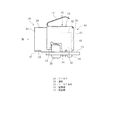
図1に示す一実施形態によるシールド10は、図2に示すナビゲーション装置などの回路基板モジュール11に適用される。この回路基板モジュール11は、金属製のフレーム12および基板13を備えている。基板13は、フレーム12に支持されている。フレーム12は、例えば金属などの導電性の材料で形成されている。フレーム12は、上枠部14、側枠部15および側枠部16を有している。側枠部15および側枠部16は、上枠部14の両端部にそれぞれ上枠部14と一体に設けられている。基板13は、これら一対の側枠部15と側枠部16との間に支持されている。以下、本実施形態中において便宜上、上枠部14側を上方とし、基板13側を下方として説明する。
シールド10は、導電性の金属によって形成されており、上述のように基板13に固定されたコネクタ20を覆う。シールド10は、図1および図5に示すようにシールド本体41、接触部42、ロック部43、ロック部44および突出部45を有している。シールド本体41は、コネクタ20の外側を覆う。本実施形態のように四角筒状のコネクタ20の場合、シールド本体41は、コネクタ20の外側において基板13側の端部、および挿入口21側の端部を除く部分を覆っている。具体的には、シールド本体41は、背面部51、側面部52、側面部53および天面部54を有している。背面部51は、シールド本体41の後壁部22の外側に位置する。すなわち、背面部51は、コネクタ20の挿入口21と反対側の端部の外側に位置する。側面部52および側面部53は、この背面部51からコネクタ20の側壁部25および側壁部26に沿ってその外側を挿入口21側へ延びている。天面部54は、背面部51からコネクタ20の基板13と反対側の面すなわち天壁部24に沿ってその外側を挿入口21側へ延びている。この天面部54は、幅方向の両端部がそれぞれ側壁部25および側壁部26と一体に接続している。側壁部25および側壁部26は、基板13側へ突出する爪部56を有している。爪部56は、基板13の保持穴57に挿入される。爪部56が保持穴57に挿入されることにより、シールド10は基板13に仮固定される。
まず、基板13にコネクタ20が取り付けられる。コネクタ20は、ねじ部材33によって基板13に固定される。ねじ部材33は、基板13側からコネクタ20のストッパ部31およびストッパ部32にねじ込まれる。基板13にコネクタ20が取り付けられると、コネクタ20の外側にシールド10が取り付けられる。シールド10は、コネクタ20の上方すなわち基板13と反対側から基板13側へ取り付けられる。シールド10の爪部56は、基板13の保持穴57に挿入される。ここで、図5に示すようにロック部43およびロック部44は、シールド本体41の側面部52および側面部53に対し傾斜している。そのため、シールド10とコネクタ20との干渉は低減される。また、ロック部43およびロック部44は、基板13側の端部から基板13までの間に距離が確保されている。そのため、シールド10と基板13との干渉も低減される。
以上説明した本発明は、上記実施形態に限定されるものではなく、その要旨を逸脱しない範囲で種々の実施形態に適用可能である。
上述の実施形態では、ロック部43およびロック部44をシールド本体41の側面部52および側面部53にそれぞれ設ける例について説明した。しかし、ロック部43、44は、シールド10とコネクタ20との相対的な移動を制限可能であれば、側面部52、53に限らず、天面部54や背面部51などに設けてもよい。また、ロック部43、44は、二つの側面部52、53の双方に限らず一方だけに設けてもよい。
Claims (6)
- 基板に固定されたコネクタを覆う導電性材料で形成されているシールドであって、
前記コネクタの外側を覆うシールド本体と、
前記シールド本体から内側へ弾性変形可能に突出して前記コネクタ側への押し付け力を有し、前記コネクタの接地端子に接する接触部と、
前記シールド本体から外側へ突出し、前記接触部が前記コネクタを押し付けることにより前記シールド本体に生じる反力で前記コネクタに接することで前記シールド本体と前記コネクタとの前記反力による相対的な移動を制限するロック部と、
前記シールド本体において前記基板と反対側の天面部に、前記シールド本体から前記基板と反対側へ弾性変形可能に突出する突出部と、
を備えるシールド。 - 基板に固定されたコネクタを覆う導電性材料で形成されているシールドであって、
前記コネクタの外側を覆うシールド本体と、
前記シールド本体から内側へ弾性変形可能に突出して前記コネクタ側への押し付け力を有し、前記コネクタの接地端子に接する接触部と、
前記シールド本体から外側へ突出し、前記接触部が前記コネクタを押し付けることにより前記シールド本体に生じる反力で前記コネクタに接することで前記シールド本体と前記コネクタとの前記反力による相対的な移動を制限するロック部と、を備え、
前記シールド本体は、前記コネクタの被挿入物が挿入される挿入口と反対側の端部に位置して前記接触部が設けられている背面部、前記背面部から前記コネクタの側方に沿って前記挿入口側へ延びている側面部、および前記背面部から前記コネクタの前記基板と反対側に沿って前記挿入口側へ延びている天面部を有し、
前記ロック部は、前記側面部にそれぞれ設けられているシールド。 - 前記ロック部は、前記基板側の端部ほど前記シールド本体との間の距離が拡大する隙間を形成している請求項1または2記載のシールド。
- 外側に突出するストッパ部によって基板に固定されたコネクタを覆う導電性材料で形成されているシールドであって、
前記コネクタの外側を覆うシールド本体と、
前記シールド本体から内側へ弾性変形可能に突出して前記コネクタ側への押し付け力を有し、前記コネクタの接地端子に接する接触部と、
前記接触部が前記コネクタを押し付けることにより前記シールド本体に生じる反力による相対的な移動を制限するために、前記接触部と対向する側に設けられ、かつ前記ストッパ部に接するように設けられているロック部と、
を備えるシールド。 - 前記シールド本体において前記基板と反対側の天面部に、前記シールド本体から前記基板と反対側へ弾性変形可能に突出する突出部をさらに備える請求項4記載のシールド。
- 前記シールド本体は、前記コネクタの被挿入物が挿入される挿入口と反対側の端部に位置して前記接触部が設けられている背面部、前記背面部から前記コネクタの側方に沿って前記挿入口側へ延びている側面部、および前記背面部から前記コネクタの前記基板と反対側に沿って前記挿入口側へ延びている天面部を有し、
前記ロック部は、前記側面部にそれぞれ設けられている請求項5記載のシールド。
Priority Applications (2)
| Application Number | Priority Date | Filing Date | Title |
|---|---|---|---|
| JP2011099506A JP5343998B2 (ja) | 2011-04-27 | 2011-04-27 | シールド |
| US13/450,569 US8672712B2 (en) | 2011-04-27 | 2012-04-19 | Shield and circuit board module having the same |
Applications Claiming Priority (1)
| Application Number | Priority Date | Filing Date | Title |
|---|---|---|---|
| JP2011099506A JP5343998B2 (ja) | 2011-04-27 | 2011-04-27 | シールド |
Publications (2)
| Publication Number | Publication Date |
|---|---|
| JP2012230857A JP2012230857A (ja) | 2012-11-22 |
| JP5343998B2 true JP5343998B2 (ja) | 2013-11-13 |
Family
ID=47068215
Family Applications (1)
| Application Number | Title | Priority Date | Filing Date |
|---|---|---|---|
| JP2011099506A Expired - Fee Related JP5343998B2 (ja) | 2011-04-27 | 2011-04-27 | シールド |
Country Status (2)
| Country | Link |
|---|---|
| US (1) | US8672712B2 (ja) |
| JP (1) | JP5343998B2 (ja) |
Families Citing this family (8)
| Publication number | Priority date | Publication date | Assignee | Title |
|---|---|---|---|---|
| US9197019B2 (en) * | 2013-03-14 | 2015-11-24 | Hubbell Incorporated | Grounding clip for electrical components |
| TWI681599B (zh) * | 2014-04-17 | 2020-01-01 | 法商內數位Ce專利控股公司 | 至少一電子配件之電氣接地配件及其電子板和電子裝置 |
| EP3134945B1 (en) | 2014-04-23 | 2019-06-12 | TE Connectivity Corporation | Electrical connector with shield cap and shielded terminals |
| JP6422815B2 (ja) * | 2015-04-21 | 2018-11-14 | 日本航空電子工業株式会社 | コネクタ |
| JP6871701B2 (ja) * | 2016-09-16 | 2021-05-12 | 日本航空電子工業株式会社 | コネクタ |
| JP6865597B2 (ja) * | 2017-02-09 | 2021-04-28 | 株式会社デンソーテン | 電子制御装置 |
| DE102020209544A1 (de) * | 2020-07-29 | 2022-02-03 | Robert Bosch Gesellschaft mit beschränkter Haftung | Elektrischer Steckverbinder, Schaltungsanordnung und Verfahren zum Ausbilden einer Schaltungsanordnung |
| CN217848378U (zh) * | 2022-07-20 | 2022-11-18 | 泰科电子(上海)有限公司 | 连接器模块和连接器 |
Family Cites Families (12)
| Publication number | Priority date | Publication date | Assignee | Title |
|---|---|---|---|---|
| JPH0626174A (ja) | 1992-07-09 | 1994-02-01 | Ig Tech Res Inc | 建築用金属板 |
| JP2596137Y2 (ja) * | 1992-09-01 | 1999-06-07 | ミツミ電機株式会社 | コネクタ |
| US6343956B2 (en) * | 2000-01-18 | 2002-02-05 | Laird Technologies Inc. | Circuit board mounted connector ground |
| JP4114867B2 (ja) * | 2003-06-10 | 2008-07-09 | 日本航空電子工業株式会社 | シールド型電気コネクタ |
| JP2006286216A (ja) | 2005-03-31 | 2006-10-19 | Auto Network Gijutsu Kenkyusho:Kk | シールドコネクタ |
| JP4184370B2 (ja) * | 2005-09-26 | 2008-11-19 | Smk株式会社 | 電気コネクタ |
| JP3122531U (ja) | 2006-04-04 | 2006-06-15 | アルプス電気株式会社 | 電子機器 |
| US7708600B2 (en) * | 2007-08-14 | 2010-05-04 | Hon Hai Precision Ind. Co., Ltd. | Compatible electrical connector |
| JP5038856B2 (ja) * | 2007-11-09 | 2012-10-03 | 日本航空電子工業株式会社 | アングル型同軸コネクタ |
| TWM354883U (en) * | 2008-04-14 | 2009-04-11 | Dragonstate Technology Co Ltd | Electrical connector |
| JP5128359B2 (ja) | 2008-04-23 | 2013-01-23 | 株式会社オートネットワーク技術研究所 | シールドコネクタ |
| US7901221B1 (en) * | 2009-01-09 | 2011-03-08 | Amazon Technologies, Inc. | Universal serial bus ground clip |
-
2011
- 2011-04-27 JP JP2011099506A patent/JP5343998B2/ja not_active Expired - Fee Related
-
2012
- 2012-04-19 US US13/450,569 patent/US8672712B2/en not_active Expired - Fee Related
Also Published As
| Publication number | Publication date |
|---|---|
| JP2012230857A (ja) | 2012-11-22 |
| US8672712B2 (en) | 2014-03-18 |
| US20120276757A1 (en) | 2012-11-01 |
Similar Documents
| Publication | Publication Date | Title |
|---|---|---|
| JP5343998B2 (ja) | シールド | |
| JP4522440B2 (ja) | 基板搭載用コネクタ及びその相手方コネクタ並びにそれらを備えた電子機器 | |
| KR101738337B1 (ko) | 커넥터 | |
| US7815467B2 (en) | Connector device | |
| JP6663565B2 (ja) | 基板用コネクタ | |
| US9583869B2 (en) | Connector and electrical connection device | |
| JP6325505B2 (ja) | コネクタ | |
| CN101911397A (zh) | 板对板连接器 | |
| CN110301021B (zh) | 蓄电单元 | |
| CN110582896B (zh) | 基板用连接器 | |
| JP7044736B2 (ja) | 電子部品ユニット | |
| JP5947640B2 (ja) | 端子金具と基板の接続構造 | |
| JP4651521B2 (ja) | コネクタ用シールドケース | |
| US20160104973A1 (en) | Shield case | |
| KR101588262B1 (ko) | 전기 커넥터 | |
| US20230063034A1 (en) | Electronic component | |
| JP6211030B2 (ja) | 電子制御装置および電子制御装置の製造方法 | |
| JP5122916B2 (ja) | 基板用コネクタ、コネクタ付回路基板及び基板収容ケース | |
| JP5923660B2 (ja) | 電子部品の組付構造及び電気接続箱 | |
| CN108370143B (zh) | 基板单元 | |
| JP2010033991A (ja) | 電子機器 | |
| US10044141B2 (en) | Connector and electrical connection device | |
| WO2014148134A1 (ja) | Usb規格準拠レセプタクルコネクタ | |
| KR102148179B1 (ko) | 커넥터 어셈블리 | |
| JP2008186734A (ja) | ジャック用ケース |
Legal Events
| Date | Code | Title | Description |
|---|---|---|---|
| A621 | Written request for application examination |
Free format text: JAPANESE INTERMEDIATE CODE: A621 Effective date: 20120824 |
|
| A131 | Notification of reasons for refusal |
Free format text: JAPANESE INTERMEDIATE CODE: A131 Effective date: 20130219 |
|
| A521 | Written amendment |
Free format text: JAPANESE INTERMEDIATE CODE: A523 Effective date: 20130409 |
|
| TRDD | Decision of grant or rejection written | ||
| A01 | Written decision to grant a patent or to grant a registration (utility model) |
Free format text: JAPANESE INTERMEDIATE CODE: A01 Effective date: 20130716 |
|
| A61 | First payment of annual fees (during grant procedure) |
Free format text: JAPANESE INTERMEDIATE CODE: A61 Effective date: 20130729 |
|
| R151 | Written notification of patent or utility model registration |
Ref document number: 5343998 Country of ref document: JP Free format text: JAPANESE INTERMEDIATE CODE: R151 |
|
| R250 | Receipt of annual fees |
Free format text: JAPANESE INTERMEDIATE CODE: R250 |
|
| R250 | Receipt of annual fees |
Free format text: JAPANESE INTERMEDIATE CODE: R250 |
|
| R250 | Receipt of annual fees |
Free format text: JAPANESE INTERMEDIATE CODE: R250 |
|
| R250 | Receipt of annual fees |
Free format text: JAPANESE INTERMEDIATE CODE: R250 |
|
| LAPS | Cancellation because of no payment of annual fees |