JP5298762B2 - Stacked semiconductor device, manufacturing method of stacked semiconductor device, and semiconductor substrate - Google Patents
Stacked semiconductor device, manufacturing method of stacked semiconductor device, and semiconductor substrate Download PDFInfo
- Publication number
- JP5298762B2 JP5298762B2 JP2008271360A JP2008271360A JP5298762B2 JP 5298762 B2 JP5298762 B2 JP 5298762B2 JP 2008271360 A JP2008271360 A JP 2008271360A JP 2008271360 A JP2008271360 A JP 2008271360A JP 5298762 B2 JP5298762 B2 JP 5298762B2
- Authority
- JP
- Japan
- Prior art keywords
- bump
- metal pattern
- bumps
- semiconductor chip
- semiconductor
- Prior art date
- Legal status (The legal status is an assumption and is not a legal conclusion. Google has not performed a legal analysis and makes no representation as to the accuracy of the status listed.)
- Active
Links
Images


Classifications
-
- H—ELECTRICITY
- H01—ELECTRIC ELEMENTS
- H01L—SEMICONDUCTOR DEVICES NOT COVERED BY CLASS H10
- H01L24/00—Arrangements for connecting or disconnecting semiconductor or solid-state bodies; Methods or apparatus related thereto
- H01L24/01—Means for bonding being attached to, or being formed on, the surface to be connected, e.g. chip-to-package, die-attach, "first-level" interconnects; Manufacturing methods related thereto
- H01L24/10—Bump connectors ; Manufacturing methods related thereto
- H01L24/12—Structure, shape, material or disposition of the bump connectors prior to the connecting process
- H01L24/14—Structure, shape, material or disposition of the bump connectors prior to the connecting process of a plurality of bump connectors
-
- H—ELECTRICITY
- H01—ELECTRIC ELEMENTS
- H01L—SEMICONDUCTOR DEVICES NOT COVERED BY CLASS H10
- H01L2224/00—Indexing scheme for arrangements for connecting or disconnecting semiconductor or solid-state bodies and methods related thereto as covered by H01L24/00
- H01L2224/01—Means for bonding being attached to, or being formed on, the surface to be connected, e.g. chip-to-package, die-attach, "first-level" interconnects; Manufacturing methods related thereto
- H01L2224/10—Bump connectors; Manufacturing methods related thereto
- H01L2224/12—Structure, shape, material or disposition of the bump connectors prior to the connecting process
- H01L2224/14—Structure, shape, material or disposition of the bump connectors prior to the connecting process of a plurality of bump connectors
-
- H—ELECTRICITY
- H01—ELECTRIC ELEMENTS
- H01L—SEMICONDUCTOR DEVICES NOT COVERED BY CLASS H10
- H01L2224/00—Indexing scheme for arrangements for connecting or disconnecting semiconductor or solid-state bodies and methods related thereto as covered by H01L24/00
- H01L2224/01—Means for bonding being attached to, or being formed on, the surface to be connected, e.g. chip-to-package, die-attach, "first-level" interconnects; Manufacturing methods related thereto
- H01L2224/10—Bump connectors; Manufacturing methods related thereto
- H01L2224/15—Structure, shape, material or disposition of the bump connectors after the connecting process
- H01L2224/16—Structure, shape, material or disposition of the bump connectors after the connecting process of an individual bump connector
Abstract
Description
本発明は、積層型半導体装置、積層型半導体装置の製造方法に関する。 The present invention relates to a stacked semiconductor device and a method for manufacturing the stacked semiconductor device.
各々に素子および回路が形成された半導体チップを複数積層した積層型の半導体装置がある(特許文献1参照)。積層型の半導体装置は、立体的な構造を採ることにより、実装面積を拡大することなく実効的な実装密度を向上させることができる。また、積層された半導体チップ相互の配線を短縮できるので、動作速度の向上にも寄与するといわれている。 There is a stacked semiconductor device in which a plurality of semiconductor chips each having an element and a circuit are stacked (see Patent Document 1). By adopting a three-dimensional structure, the stacked semiconductor device can improve the effective mounting density without increasing the mounting area. In addition, it is said that the wiring between the stacked semiconductor chips can be shortened, which contributes to an improvement in operation speed.
図19は、ウエハとウエハを積層するWafer-to-Wafer(W2W)プロセスの代表例を示す図である。なお、図19(a)〜(f)はウエハの一部の断面の様子を示すものであるが、全ての作業はウエハ全体に対して同時に行われる。 FIG. 19 is a diagram illustrating a typical example of a wafer-to-wafer (W2W) process for stacking wafers. FIGS. 19A to 19F show the state of a partial cross section of the wafer, but all operations are performed simultaneously on the entire wafer.
表面にSiO2、Si2N4,ポリイミド等の絶縁層1902が形成されたSi基板1901の内部に公知の方法によりトランジスタ回路1903を形成する。そして、絶縁層1902内に、Alパッド1904,1905を形成する(a)。次にRIE(Reactive-Ion-Etching)により絶縁層1902とSi基板1901とに穴あけを行い、その中に導電体(例えばCu)を充填する。この導電体は、後に積層されるウエハ同士の電気接続を行うためのものでありTSV(Through Si Via)と呼ばれる。なお、TSV1906の周りには、SiO2等からなる絶縁膜と、TiN等からなるバリアメタルが形成され、Si基板1901との絶縁を図るようになっているが、ここでは図示を省略している(b)。次に、TSV1906の露出部分にバンプ1907を形成する(c)。バンプ1907は例えばSnAgCu等で形成されている。
A
続いて、(c)のようにして形成されたウエハの表面同士が相対するようにして向き合わせ、バンプ1907同士を接合する(d)。接合されたバンプ1907の厚みは、1つのウエハに形成されたものの厚さの2倍となるはずであるが、接合に際して押圧されるので、一般にそれよりも少し薄くなる。次に、このように接合された2つのウエハの一方の裏面をCMP等により研磨し、TSV1906を露出させる(e)。この工程を薄化工程という。露出したTSV1906の表面に新たにバンプ1907を形成し、これに、(c)と同じ構造を有するウエハのバンプ1907を接合することにより、3枚のウエハ同士を接合する(f)。
Subsequently, the wafers formed as shown in (c) are faced to face each other, and the
以下、3枚目のウエハの裏面を研磨してTSV1906を露出させ、その表面に新たにバンプ1907を形成し、これに、(c)と同じ構造を有するウエハのバンプ1907を接合することにより、4枚のウエハ同士を接合する。これを繰り返して、多数層の積層を有する積層型半導体装置が形成される。
立体的な実装密度が高くなった場合、発熱源としての回路または素子の密度も高くなる。このため、積層構造の内部には熱分布が生じやすくなり、動作の安定性にも分布が生じがちになる。即ち、積層型半導体装置の安定した動作には、効率の高い放熱構造が求められる。 When the three-dimensional mounting density is increased, the density of a circuit or element as a heat source is also increased. For this reason, heat distribution tends to occur inside the laminated structure, and distribution tends to occur in operation stability. In other words, a highly efficient heat dissipation structure is required for stable operation of the stacked semiconductor device.
上記課題を解決するために、本発明の第1の態様においては、回路領域と、回路領域の素子と電気的に接続された第1のバンプ群と、回路領域を囲んだパターンを形成する、回路領域の素子とは電気的に接続されない第2のバンプ群とをそれぞれ備える複数の半導体チップを、第1のバンプ群の少なくとも対向しあう一部同士、および第2のバンプ群の少なくとも対向しあう一部同士を接合して積層した積層型半導体装置が提供される。 In order to solve the above problems, in the first aspect of the present invention, a circuit region, a first bump group electrically connected to an element in the circuit region, and a pattern surrounding the circuit region are formed. A plurality of semiconductor chips each including a second bump group that is not electrically connected to an element in the circuit region are arranged so that at least a part of the first bump group that faces each other and at least the second bump group faces each other. Provided is a stacked semiconductor device in which a part of each other is bonded and stacked.
また、第2の態様においては、回路領域を有する半導体チップに、回路領域の素子と電気的に接続された第1のバンプ群と、回路領域を囲んだパターンを形成する前記回路領域の素子とは電気的に接続されない第2のバンプ群とを設けるバンプ群形成ステップと、バンプ群形成ステップを経た複数の半導体チップを積み重ね、対向する第1のバンプ群同士、および対向する第2のバンプ群同士を接合する積層ステップとを備える積層型半導体装置の製造方法が提供される。 Further, in the second aspect, a first bump group electrically connected to the circuit region element and a circuit region element forming a pattern surrounding the circuit region on a semiconductor chip having the circuit region, Is a bump group forming step for providing a second bump group that is not electrically connected, and a plurality of semiconductor chips that have undergone the bump group forming step are stacked, and the first bump groups facing each other and the second bump group facing each other There is provided a manufacturing method of a stacked semiconductor device including a stacking step of bonding together.
なお、上記の発明の概要は、本発明の必要な特徴の全てを列挙したものではない。また、これらの特徴群のサブコンビネーションもまた、発明となりうる。 It should be noted that the above summary of the invention does not enumerate all the necessary features of the present invention. In addition, a sub-combination of these feature groups can also be an invention.
以下、発明の実施の形態を通じて本発明を説明するが、以下の実施形態は特許請求の範囲にかかる発明を限定するものではない。また、実施形態の中で説明されている特徴の組み合わせの全てが発明の解決手段に必須であるとは限らない。 Hereinafter, the present invention will be described through embodiments of the invention, but the following embodiments do not limit the invention according to the claims. In addition, not all the combinations of features described in the embodiments are essential for the solving means of the invention.
(第1の実施形態)
素子および回路が形成された半導体チップを3次元構造へと展開する3D−LSIは、およそ3つに分類される。一つはKGD(Known-Good-Die)のみを低精度のダイボンダで積層しワイヤボンドで半導体チップ間を接続する「簡易Chip積層」であり、一つはバーンイン・テストを行った良品パッケージを積層する「パッケージ型積層」である。そしてもう一つが、Siウエハ上に素子間の貫通電極を設けウエハもしくは半導体チップ同士を直接接続して形成する「貫通電極方積層(以下、TSV:Through Si Via積層と言う)」である。
(First embodiment)
There are roughly three types of 3D-LSIs that develop a semiconductor chip on which elements and circuits are formed into a three-dimensional structure. One is “simple chip stack” in which only KGD (Known-Good-Die) is stacked with a low-accuracy die bonder and the semiconductor chips are connected by wire bonding. This is a “package type stacking”. The other is “through electrode side lamination (hereinafter referred to as TSV: Through Si Via lamination)” in which a through electrode between elements is provided on a Si wafer and the wafer or semiconductor chips are directly connected to each other.
さらにTSV積層は以下の3つの方法に分類できる。すなわち、KGD同士を積層するChip-to-Chip(C2C)、ウエハ上にKGDを搭載するChip-to-Wafer(C2W)、およびウエハ同士を直接貼り合わせるWafer-to-Wafer(W2W)である。 Furthermore, TSV lamination can be classified into the following three methods. That is, a chip-to-chip (C2C) for stacking KGDs, a chip-to-wafer (C2W) for mounting KGD on a wafer, and a wafer-to-wafer (W2W) for directly bonding wafers together.
本実施形態では、C2CによるTSV積層のプロセスを用いることとし、以下図面を用いて説明する。 In the present embodiment, a process of TSV stacking by C2C is used and will be described below with reference to the drawings.
図1は、積層される半導体チップ100を模式的に示す正面図である。この半導体チップ100の内側には、回路を構成する素子および配線等が実質的に配置されている回路領域101を備える。そして、回路領域101の内側には、素子と電気的に接続された第1のバンプ群としての複数の回路バンプ102が形成されている。これらの回路バンプは、後述するTSV104の先端に設けられている。
FIG. 1 is a front view schematically showing
回路領域101の外側には、回路領域101に形成されている素子と電気的に接続されていない第2のバンプ群としての複数のダミーバンプ103が形成されている。本実施形態においては、ダミーバンプ103も回路バンプ102と同様に、TSV104の先端に設けられている。
A plurality of
図示の例では、回路バンプ102もダミーバンプ103も規則的なマトリックス状に配されているが、規則的に配される必要は無い。回路領域101内に形成される回路バンプは、回路に要求される機能によって配される素子および配線等に応じて形成されるので、その配置は規則的になるとは限らない。また、ダミーバンプ103は、後述するように、放熱の観点等から配されるので、特に整列していることが要求されるわけでは無い。ただし、図示の例からもわかるように、回路領域101の内側に配される回路バンプ102の単位面積当たりの分布密度と、外側に配されるダミーバンプ103の単位面積当たりの分布密度を比較すると、ダミーバンプ103のそれの方が大きいことが好ましい。これは、回路領域101で発生した熱をより効率的に逃がすためと、半導体チップ間の接合力を増強するために、このように構成することが好ましいからである。
In the illustrated example, both the
図2は、半導体チップ100の、図1に示すA−Aのうち、端部付近の断面図である。回路領域101内に形成されたTSV104は、アルミ薄膜配線203を介して、素子としてのトランジスタ回路204と接続され、回路の電気接続を行う役割を果たしている。TSV104は、RIE(Reactive-Ion-Etching)により空けられた穴に導電体(例えばCu)が充填されて形成される。TSV104の周りには、SiO2からなる絶縁膜201と、TiN等からなるバリアメタル202が形成され、Si基板との絶縁を図るように構成されている。なお、絶縁膜201は、Si基板の表面にも連続して形成されている。回路バンプ102は、TSV104の両端に設けられ、積層される他の半導体チップ等との接合に用いられ、電気接続配線としての役割を果たす。
2 is a cross-sectional view of the
回路領域101外に形成されたTSV104は、図示するようにトランジスタ回路204とは接続されておらず、電気的には回路領域101内の素子および配線等とは絶縁されている。なお、TSV104は回路領域101の内外に関わらず同一の工程で形成されるので、回路領域101外のTSV104も、その周りにSiO2からなる絶縁膜201と、TiN等からなるバリアメタル202が形成されている。
The TSV 104 formed outside the
ダミーバンプ103は、回路領域101外のTSV104の両端に設けられ、積層されれる他の半導体チップ等との接合に用いられ、半導体チップ間の熱伝導と接合力強化に寄与する。
The
回路バンプ102もダミーバンプ103も、同一工程によりTSV104の先端に形成される。そのため、回路バンプ102の直径R1とダミーバンプ103の直径R2は同じであることが好ましい。
Both the
また、回路バンプ102もダミーバンプ103も、相対する他の半導体チップに形成されたそれぞれのバンプに押圧されて接合されるので、互いに接触するときには、その接触面が同一平面であることが好ましい。もし、それぞれの高さが異なると、一部のバンプ同士は接触することがなく、また、一部のバンプ同士は過押圧されるという状況が生じる恐れがあるからである。回路バンプ102同士が接触しなければ、信号の寸断に繋がるため積層型半導体装置としての機能そのものが果たせない。ダミーバンプ103同士が接触しなければ、熱伝導が途切れるために放熱が効率的に行われない、もしくは製造工程において接合力不足により半導体チップ同士が剥がれるという不都合が生じる。逆にバンプ同士が過押圧されると、バンプの破壊に繋がる恐れがある。したがって、回路バンプ102もダミーバンプ103も、その先端の高さは半導体チップ100の表面からHであり、同一の高さである。ただし、同一の高さにすることが難しい場合には、信号線の確実な導通を得るために、回路バンプ102のほうを若干高くしておくことが好ましい。
In addition, since the circuit bumps 102 and the dummy bumps 103 are pressed and bonded to the respective bumps formed on other semiconductor chips facing each other, it is preferable that the contact surfaces are the same plane when contacting each other. If the heights are different, some bumps do not contact each other, and some bumps may be over-pressed. If the circuit bumps 102 are not in contact with each other, the signal will be cut off, and the function itself as a stacked semiconductor device cannot be performed. If the dummy bumps 103 are not in contact with each other, heat conduction is interrupted and heat dissipation is not performed efficiently, or semiconductor chips are peeled off due to insufficient bonding force in the manufacturing process. Conversely, if the bumps are over-pressed, there is a risk that the bumps will be destroyed. Therefore, the height of the tip of both the
なお、回路バンプ102もダミーバンプ103も、例えばSnAgCu等の同一材料により形成されている。 The circuit bumps 102 and the dummy bumps 103 are made of the same material such as SnAgCu.
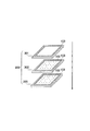
次に、図3を用いて、上記のように形成されている半導体チップを積層する工程について説明する。図3は、半導体チップの積層工程を説明する概念図である。 Next, the process of stacking the semiconductor chips formed as described above will be described with reference to FIG. FIG. 3 is a conceptual diagram illustrating a semiconductor chip stacking process.
積層される半導体チップ群300は、最上面の半導体チップ301、中間面の半導体チップ302、および最下面の半導体チップ303より構成される。中間面の半導体チップ302は、1枚とは限らず、2枚以上を積層しても良い。また、中間面の半導体チップ302と最下面の半導体チップ303は、図1および図2を用いて説明した半導体チップ100と同等に構成されている。
The stacked
最上面の半導体チップ301は、中間面の半導体チップ302と対向する面とは反対の面で、後述するように例えばCuから成るヒートスプレッタ401と接触する。ヒートスプレッタ401が導電体である場合、ヒートスプレッタ401と接触する面には、電気接続配線としての役割を果たす回路バンプ102を設けることができない。したがって、最上面の半導体チップ301については、トランジスタ回路204が形成されている面を、中間面の半導体チップ302側に向け、かつ、回路バンプ102をTSV104を用いることなく形成している。そのため、図示するように、ヒートスプレッタ401と接触する面には、回路バンプ102が存在しない。一方、ダミーバンプ103は、ヒートスプレッタ401と積極的に接触して放熱の効率を上げることが好ましいので、半導体チップ100のダミーバンプ103と同様にTSV104を用いて形成される。
The
そして、このように準備された最上面の半導体チップ301、中間面の半導体チップ302、および最下面の半導体チップ303を、対向する回路バンプ102同士、およびダミーバンプ103同士を矢印方向に接触させて押圧し、互いに接合する。
Then, the
なお、回路バンプ102同士の接合については、積層型半導体装置として機能させるために必要な電気的接続を行うものなので、一方の回路バンプ102に対向して、他方の回路バンプ102が存在しなければならないというものではない。すなわち、接続が必要な回路バンプ102同士が接続されるのであって、接続されていない回路バンプ102が存在しても良い。その意味では、対向する半導体チップのそれぞれに形成されている複数の回路バンプのうち、少なくとも一部の回路バンプ102同士が接合していれば良い。
Note that the circuit bumps 102 are joined to each other because electrical connection necessary for functioning as a stacked semiconductor device is performed, so that one
同様に、ダミーバンプ103同士の接合についても、予定される放熱効果と接合力強化の効果が得られれば良いので、必要な数のダミーバンプ103同士が接合していれば良い。その意味では、対向する半導体チップのそれぞれに形成されている複数のダミーバンプ103のうち、少なくとも一部のダミーバンプ103同士が接合していれば良い。 Similarly, the dummy bumps 103 may be bonded together as long as the expected heat dissipation effect and the effect of strengthening the bonding force can be obtained. In that sense, it is only necessary that at least some of the dummy bumps 103 are bonded to each other among the plurality of dummy bumps 103 formed on each of the opposing semiconductor chips.
また、最上面の半導体チップ301の、ヒートスプレッタ401と接触する面側に絶縁層を設けるなどして、TSV104が直接ヒートスプレッタ401と接触しないようにすれば、TSV104を用いることができる。このように構成すれば、中間面の半導体チップ302と対向する面の回路バンプ102を、TSV104の先端に形成することができる。
Further, the
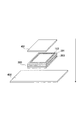
図4は、上記のように形成される半導体チップ群300と他の構成要素を積層する工程を説明する概念図である。
FIG. 4 is a conceptual diagram illustrating a process of stacking the
ヒートスプレッタ401は、ダミーバンプ103を経由して伝えられる熱を外部に放熱する。したがって、上述のように形成されている最上面の半導体チップ301に設けられたダミーバンプ103に、ヒートスプレッタ401を矢印方向に押しあてて接合する。ヒートスプレッタ401は、放熱特性が良い素材を用いる。例えばCuが好ましい。
The
そして、これら接合されたヒートスプレッタ401と半導体チップ群300を、ベース402へ接合する。具体的には、半導体チップ群300を構成する最下面の半導体チップ303の、ベース402との接合面には回路バンプ102およびダミーバンプ103が設けられており、これらをベース402へ矢印方向に押圧して接合する。なお、ベース402は絶縁体で形成されているので、回路バンプ102が接触しても問題は無い。
Then, the bonded
図5は、このようにして積層された積層型半導体装置の断面図である。上述のようにして接合・積層されたヒートスプレッタ401、半導体チップ群300、およびベース402のそれぞれの間には、わずかながら間隙を生じている。このような間隙を封止するため、有機物を材料とするアンダーフィル501を充填する。具体的には、間隙の側方から液状のアンダーフィル501を流入し、固化させる。そしてさらに、その側方をモールド部材502で密封する。
FIG. 5 is a cross-sectional view of the stacked semiconductor device stacked in this manner. A slight gap is generated between each of the
図示するように、アンダーフィル501は、ヒートスプレッタ401、半導体チップ群300、およびベース402のそれぞれが、回路バンプ102、ダミーバンプ103によって接合されるときに生じる間隙に充填されている。そして、その側方は、モールド部材502により密封されている。
As shown in the drawing, the
図6は、これまで説明してきた各工程をまとめた、本実施形態における積層型半導体装置の製造工程を示すフロー図である。 FIG. 6 is a flowchart showing manufacturing steps of the stacked semiconductor device according to the present embodiment, which summarizes the steps described so far.
まず、ステップS601で、TSV104が形成される。具体的には、RIEにより空けられた穴に導電体が充填されて形成される。TSV104の形成は、回路領域101の内外に関わらず、同一工程により行われる。次に、ステップS602で、回路バンプ102とダミーバンプ103が形成される。これらは、必要な個数に応じてそれぞれ複数個のバンプ群として形成される。また、回路バンプ102とダミーバンプ103は、共に一度の工程で同時に形成される。本実施形態においては、C2CのTSV積層として説明しているが、TSVの形成(ステップS601)およびバンプ群の形成(ステップS602)は、半導体チップに切断される前のウエハ単位で行っても良い。
First, in step S601, the
そして、ステップS603で、切断された半導体チップのそれぞれが重ねあわされて積層、接合される。具体的には、図3を用いて説明したように、それぞれ対向する面に形成されている、対応する回路バンプ102同士、および対応するダミーバンプ103同士が接合されることにより実現される。このようにして積層された半導体チップ群300にはさらに、ステップS604で、その端面のそれぞれに接触するように、ヒートスプレッタ401とベース402が接合される。その後、ステップS605で、アンダーフィル501により層間の間隙が封止され、そして側方がモールド部材502により密封されて、一連の工程を終了する。
In step S603, the cut semiconductor chips are stacked and bonded together. Specifically, as described with reference to FIG. 3, this is realized by bonding corresponding circuit bumps 102 and corresponding dummy bumps 103 formed on the opposing surfaces. In step S604, the
なお、半導体チップ群300とヒートスプレッタ401との接合については、最上面の半導体チップ301に設けられたダミーバンプ103に、ヒートスプレッタ401を押しあてて接合するものとして説明したが、これに限られない。Si基板はそれ自体熱伝導率が高いので、ヒートスプレッタ401との接合面をダミーバンプ103も形成せずにフラットとし、熱伝導率の高い接着剤等により接合するように構成しても良い。この場合は、比較的熱伝導率が低いアンダーフィルが、ヒートスプレッタ401と最上面の半導体チップ301の間に介在することがないので、ダミーバンプ103の個数を確保できない場合には好ましいといえる。
Note that the bonding between the
以上の本実施形態にでは、半導体チップ100、最上面の半導体チップ301、中間面の半導体チップ302、および最下面の半導体チップ303は、それぞれが元々比較的薄い基板にTSV104等の各要素が形成されていることを前提として説明した。すなわち、本実施形態の半導体チップに対しては、図19を用いて説明した薄化工程を必要としない。しかし、比較的厚い基板を用い、薄化工程を組み入れて半導体チップ群300を積層するようにしても良い。この場合、ステップS601からステップS603の工程を多少変更する。
In the above embodiment, the
具体的には、最上面の半導体チップ301の裏面側にトランジスタ回路204等の要素を形成し、TSV104を形成し、その上にバンプ群を形成する。一方、中間面の半導体チップ302のうち、最上面の半導体チップ301と接合される表面側に、トランジスタ回路204等の要素、TSV104およびバンプ群を形成する。そして、それぞれのバンプ群を接合して、最上面の半導体チップ301と中間面の半導体チップ302を積層する。この段階では、まだ互いに接合された面と反対側のそれぞれの面は、TSV104が露出しておらず、バンプ群も形成されていない状態である。
Specifically, an element such as a
そして、接合した後に中間面の半導体チップ302の裏面側をCMP等により研磨し、TSV104を露出させる。つまり、中間面の半導体チップ302に対して薄化工程を行う。そして、露出したTSV104に対してバンプ群を形成する。
Then, after bonding, the back surface side of the
一方、最下面の半導体チップ303のうち、中間面の半導体チップ302と接合される表面側に、トランジスタ回路204等の要素、TSV104およびバンプ群を形成する。そして、それぞれのバンプ群を接合して、すでに最上面の半導体チップ301と一体となっている中間面の半導体チップ302と、最下面の半導体チップ303を積層する。この段階では、最下面の半導体チップ303のうち、中間面の半導体チップ302と接合された面と反対側の面である裏面は、TSV104が露出しておらず、バンプ群も形成されていない状態である。
On the other hand, elements such as the
そして、接合した後に最下面の半導体チップ303の裏面側をCMP等により研磨し、TSV104を露出させる。つまり、最下面の半導体チップ303に対して薄化工程を行う。そして、露出したTSV104に対してバンプ群を形成する。
After bonding, the back surface side of the
次に、最上面の半導体チップ301の表面側をCMP等により研磨し、TSV104を露出させる。つまり、最上面の半導体チップ301に対して薄化工程を行う。そして、露出したTSV104に対してバンプ群を形成する。
Next, the surface side of the
このようにして、比較的厚い基板を用いて半導体チップ群300を積層することができる。もちろん、中間面の半導体チップ302は、上記のように薄化工程を繰り返して何層も積層することができる。さらに、薄化工程を組み入れる上記手法においても、C2CのTSV積層に限らず、半導体チップに切断される前のウエハ単位で行う、W2WのTSV積層であっても良い。
In this way, the
以上本実施形態によれば、積層構造の内部に発生した熱を、TSV104およびダミーバンプ103を放熱パスとしてヒートスプレッタ401に導き、外部へ逃がすことができるので、積層型半導体装置の安定した動作を期待できる。また、ダミーバンプ103をTSVの先端に点状に形成したので、層間の接合後には側方からみて間隙が生じる。この側方の間隙を利用すると、アンダーフィル501の充填を、作業が比較的容易である流入により行える。
As described above, according to the present embodiment, the heat generated in the stacked structure can be guided to the
以下、第1の実施形態の変形例としていくつかの実施形態を説明する。共通する符号については第1の実施形態の構成と同一であるためその説明を省略し、それぞれの実施形態において特徴をなす異なる部分を説明する。 Hereinafter, some embodiments will be described as modifications of the first embodiment. Since the common reference numerals are the same as those of the first embodiment, the description thereof will be omitted, and different parts that characterize the respective embodiments will be described.
(第2の実施形態)
図7は、第2の実施形態に係る、半導体チップ100の端部付近の断面図である。本実施形態における半導体チップ100の正面図は、図1を用いて説明した第1の実施形態の半導体チップ100の正面図と同じである。
(Second Embodiment)
FIG. 7 is a cross-sectional view of the vicinity of the end of the
図示するように、本実施形態においては、ダミーバンプ103は、TSVの先端に形成されるのではなく、絶縁膜201の上、もしくは直接Si基板の上に設けられたバッファメタル701の上に形成される。このように構成することにより、Si基板はそれ自体熱伝導率が高いのでTSVに準じた放熱特性を期待でき、また、RIEによる穴の形成時間を短縮できるという効果を得る。
As shown in the figure, in this embodiment, the
(第3の実施形態)
図8は、第3の実施形態に係る、半導体チップ800を模式的に示す正面図である。回路領域101、複数の回路バンプ102(第1のバンプ群)、複数のダミーバンプ103(第2のバンプ群)の配置については第1の実施形態と同等であるが、メタルパターン801を設けた点が第1の実施形態とは異なる。具体的には、回路領域101を閉じて囲むように外側にメタルパターン801が配され、その上にダミーバンプ103が存在するように構成されている。
(Third embodiment)
FIG. 8 is a front view schematically showing a
図9は、半導体チップ800の、図8に示すB−Bのうち、端部付近の断面図である。ダミーバンプ103をTSV104の先端に設ける点は、図2を用いて説明した第1の実施形態と同様である。本実施形態においては、図2の構成に加えて、上下面のそれぞれで、複数のダミーバンプ103が共に載置されるようにメタルパターン801が更に設けられている。なお、メタルパターンは、例えば、PVD(Physical Vapor Deposition)によりTiNを蒸着させて形成される。
FIG. 9 is a cross-sectional view of the
このように構成すると、ダミーバンプ103の大きさをコントロールすることにより、接合時の押圧によって、層間の対向するダミーバンプ103同士のみならず、隣接するダミーバンプ103同士も接合させることができる。その結果、対向する2枚の半導体チップ800のそれぞれに設けられたメタルパターン801の間には、複数のダミーバンプが押圧されて一体となった壁が形成されることになる。つまり、接合後には、メタルパターン801上で隙間の無い接合層が形成されると言える。この接合層は、回路領域101を内包して外部空間と遮断する。したがって、回路領域101の保護の観点から好ましいと言える。
With this configuration, by controlling the size of the dummy bumps 103, not only the dummy bumps 103 facing each other but also the adjacent dummy bumps 103 can be bonded together by pressing during bonding. As a result, a plurality of dummy bumps are pressed to form an integral wall between the
なお、本実施形態においては、すべてのダミーバンプ103がメタルパターン801上に配される構成を説明したが、これに限らない。即ち、一部のダミーバンプ103がメタルパターン801上に無くても、メタルパターン801上のダミーバンプ103で接合層が形成されれば、回路領域101の保護は達成されるからである。
In the present embodiment, the configuration in which all the dummy bumps 103 are arranged on the
また、この場合には、予めシート状に加工されたアンダーフィル501を、メタルパターン801の内部に配置しておくことで、層間の接合時に充填を行うことができる。もしくは、インクジェット方式により、アンダーフィル501を予めメタルパターン801の内部に滴下しておくことでも、層間の接合時に充填を行うことができる。
In this case, the
本実施形態におけるメタルパターン801は、半導体チップ800の外周部より離間させて配置されているが、このように配置することで、メタルパターン801は、ウエハ状態から半導体チップ状態へ切断されるときの切断しろに影響を受けることが無い。したがって、接合層の一定の幅を常に確保できることから、予定される放熱効果を確実に得ることが期待できる。
The
(第4の実施形態)
図10は、第4の実施形態に係る、半導体チップ800の端部付近の断面図である。本実施形態における半導体チップ800の正面図は、図8を用いて説明した第3の実施形態の半導体チップ800の正面図と同じである。
(Fourth embodiment)
FIG. 10 is a cross-sectional view of the vicinity of the end portion of the
図示するように、本実施形態においては、ダミーバンプ103は、TSVの先端に形成されるのではなく、絶縁膜201の上、もしくは直接Si基板の上に設けられたメタルパターン801の上に形成される。このように構成することにより、Si基板はそれ自体熱伝導率が高いのでTSVに準じた放熱特性を期待でき、また、RIEによる穴の形成時間を短縮できるという効果を得る。
As shown in the figure, in this embodiment, the
(第5の実施形態)
図11は、第5の実施形態に係る、半導体チップ1100を模式的に示す正面図である。回路領域101、回路バンプ102(第1のバンプ群)の配置については第3の実施形態と同等であるが、メタルパターン1101の上にダミーバンプ群(第2のバンプ群)として一体的にダミーバンプ層1103を設けた点が第3の実施形態とは異なる。回路領域101を閉じて囲むように外側にメタルパターン1101が配されている点は、第3の実施形態におけるメタルパターン801と同様である。
(Fifth embodiment)
FIG. 11 is a front view schematically showing a
図12は、半導体チップ1100の、図11に示すC−Cのうち、端部付近の断面図である。図示するように、本実施形態においては、ダミーバンプ層1103は、TSVを用いることなく、絶縁膜201の上、もしくは直接Si基板の上に設けられたメタルパターン1101の上に形成される。このように構成することにより、接合前からメタルパターン1101上で隙間の無い接合層が確実に形成されることが期待できる。
FIG. 12 is a cross-sectional view of the
また、本実施形態におけるメタルパターン1101は、半導体チップ1100の外周部より離間させて配置されているが、このように配置することで、メタルパターン1101は、ウエハ状態から半導体チップ状態へ切断されるときの切断しろに影響を受けることが無い。したがって、ダミーバンプ層1103の一定の幅を常に確保できることから、予定される放熱効果を確実に得ることが期待できる。
In addition, the
(第6の実施形態)
図13は、第6の実施形態に係る、半導体チップ1100を模式的に示す正面図である。回路領域101、回路バンプ102(第1のバンプ群)の配置については第5の実施形態と同等である。また、メタルパターン1301の上にダミーバンプ群(第2のバンプ群)として一体的にダミーバンプ層1303を設けた点も第5の実施形態と同等であるが、本実施形態におけるメタルパターン1301の形状が第5の実施形態のそれと異なる。具体的には、回路領域101を完全に閉じて囲むのではなく、数箇所(図では4箇所)でパターンが寸断されている。このように構成することで、半導体チップを接合した後には寸断箇所が回路領域と連通する空隙となり、アンダーフィル501の充填を、作業が比較的容易である流入により行える。同時に、回路領域101の大部分はダミーバンプ層1303で囲まれるので、完全に囲まれた構成に準じた回路領域101の保護が期待できる。
(Sixth embodiment)
FIG. 13 is a front view schematically showing a
(第7の実施形態)
図14は、第7の実施形態に係る、半導体チップ1400を模式的に示す正面図である。メタルパターン1401の上にダミーバンプ群(第2のバンプ群)として一体的にダミーバンプ層1403を設けた点は第5の実施形態と同等であるが、本実施形態におけるメタルパターン1401の位置が第5の実施形態のそれと異なる。第5の実施形態においては、メタルパターン1101を半導体チップ1100の外周部から離間させて配置しているが、本実施形態においては外周部に接するように配置されている。
(Seventh embodiment)
FIG. 14 is a front view schematically showing a
図15は、半導体チップ1400の、図14に示すD−Dのうち、端部付近の断面図である。図示するように、本実施形態においては、ダミーバンプ層1403は、TSVの先端と、メタルパターン1401の上に形成される。このように構成することにより、接合前からメタルパターン1401上で隙間の無い接合層が確実に形成されることが期待できると同時に、より効率的な放熱が可能となる。なお、図示するように、TSV104は、外周部に接しないようにすることが好ましい。
15 is a cross-sectional view of the
また、本実施形態におけるメタルパターン1401は、半導体チップ1400の外周部と接して配置されているが、このように配置することで、回路領域101を広く確保することができ、ひいては回路バンプ102の配置の自由度も増す。
In addition, the
(第8の実施形態)
図16は、第8の実施形態に係る、半導体チップ1600を模式的に示す正面図である。回路領域101の配置については第5の実施形態と同等である。また、メタルパターン1601の上にダミーバンプ群(第2のバンプ群)として一体的にダミーバンプ層1603を設けた点も第5の実施形態と同等であるが、本実施形態におけるメタルパターン1601の形状および回路バンプ1602の配置が第5の実施形態のそれと異なる。
(Eighth embodiment)
FIG. 16 is a front view schematically showing a
これまでの実施形態においては、回路バンプ102は、規則的なマトリックス状に配されているものとして説明してきたが、実際には回路に要求される機能によって配される素子および配線等に応じて形成されるので、その配置は規則的になるとは限らない。本実施形態においては、回路バンプ1602が、回路領域101内で偏って配置された場合を説明する。
In the embodiments so far, the circuit bumps 102 have been described as being arranged in a regular matrix. However, in actuality, depending on the elements and wirings arranged depending on the functions required for the circuit, etc. Since it is formed, its arrangement is not always regular. In the present embodiment, a case where the circuit bumps 1602 are arranged in a biased manner in the
回路バンプ1602が偏って配置されると、積層型半導体装置の動作時には、熱の発生やその後の分布にも偏りが生じる。そこで本実施形態においては、回路領域101内で発熱の大きい領域に隣接するメタルパターン1601の幅を、他の領域に隣接するメタルパターン1601の幅よりも大きくする。具体的には、図示するように、回路領域101内で回路バンプ1602の密度が高い領域を発熱の大きい領域と想定し、この領域付近のメタルパターン1601の幅を大きくしている。このように構成することで、より効率的な放熱パスを形成することが可能となる。
If the circuit bumps 1602 are arranged in a biased manner, the generation of heat and the subsequent distribution are also biased during the operation of the stacked semiconductor device. Therefore, in the present embodiment, the width of the
(第9の実施形態)
図6を用いて説明した半導体チップの積層についてはC2Cとして説明したが、上述のように、積層型半導体装置の製造工程としては、W2Wも考えられる。本実施形態においては、W2Wにより積層する工程の一例について説明する。
(Ninth embodiment)
Although the semiconductor chip stacking described with reference to FIG. 6 has been described as C2C, as described above, W2W is also conceivable as a manufacturing process of the stacked semiconductor device. In this embodiment, an example of the process of laminating by W2W will be described.
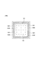
図17は、本実施形態における、半導体チップ領域1700が複数形成された1枚のウエハ1701の概要を示す図である。半導体チップ領域1700は、ウエハ1701の切断線すなわち、スクライブラインによって切断された後には、個別の半導体チップとなる。また、ウエハ1701には、すでに複数の回路バンプおよび複数のダミーバンプであるバンプ群が形成されている。なお、本実施形態においては、第7の実施形態として説明したような、メタルパターンが半導体チップの外周部に接するものを想定する。
FIG. 17 is a view showing an outline of one
このように形成されるウエハ1701のある領域Eに着目すると、半導体チップ領域1700としての、4つの半導体チップ領域1711、1712、1713および1714が、互いに隣接している。
When attention is paid to an area E of the
図18は、図17の領域Eの拡大図である。本実施形態においては、メタルパターンが半導体チップの外周部に接しているので、それぞれの半導体チップ領域の境界部はメタルパターンである。そして、このメタルパターン上に想定されるスクライブライン1721とスクライブライン1722で切断されることにより、個々の半導体チップとして分割される。そして、その交点には、指標としてアライメントマーク1730が設けられており、ウエハとウエハを積層するときの位置合せの基準となる。ウエハ積層装置は、このアライメントマーク1730をターゲットとして対向するウエハ同士を接合する。このように構成することにより、メタルパターンを位置合せのためのアライメントマークとしても利用することができる。なお、アライメントマーク1730は、メタルパターンが蒸着されないよう、十字にマスクされることにより設けられる。なお、アライメントマーク1730は、十字に限らず、その他の図形であっても良い。
FIG. 18 is an enlarged view of a region E in FIG. In the present embodiment, since the metal pattern is in contact with the outer peripheral portion of the semiconductor chip, the boundary portion of each semiconductor chip region is a metal pattern. And it cut | disconnects by the
以上、本発明を実施の形態を用いて説明したが、本発明の技術的範囲は上記実施の形態に記載の範囲には限定されない。上記実施の形態に、多様な変更または改良を加えることが可能であることが当業者に明らかである。その様な変更または改良を加えた形態も本発明の技術的範囲に含まれ得ることが、特許請求の範囲の記載から明らかである。 As mentioned above, although this invention was demonstrated using embodiment, the technical scope of this invention is not limited to the range as described in the said embodiment. It will be apparent to those skilled in the art that various modifications or improvements can be added to the above-described embodiment. It is apparent from the scope of the claims that the embodiments added with such changes or improvements can be included in the technical scope of the present invention.
特許請求の範囲、明細書、および図面中において示した装置、システム、プログラム、および方法における動作、手順、ステップ、および段階等の各処理の実行順序は、特段「より前に」、「先立って」等と明示しておらず、また、前の処理の出力を後の処理で用いるのでない限り、任意の順序で実現しうることに留意すべきである。特許請求の範囲、明細書、および図面中の動作フローに関して、便宜上「まず、」、「次に、」等を用いて説明したとしても、この順で実施することが必須であることを意味するものではない。 The order of execution of each process such as operations, procedures, steps, and stages in the apparatus, system, program, and method shown in the claims, the description, and the drawings is particularly “before” or “prior to”. It should be noted that the output can be realized in any order unless the output of the previous process is used in the subsequent process. Regarding the operation flow in the claims, the description, and the drawings, even if it is described using “first”, “next”, etc. for convenience, it means that it is essential to carry out in this order. It is not a thing.
100 半導体チップ、101 回路領域、102 回路バンプ、103 ダミーバンプ、104 TSV、201 絶縁膜、202 バリアメタル、203 アルミ薄膜配線、204 トランジスタ回路、300 半導体チップ群、301 最上面の半導体チップ、302 中間面の半導体チップ、303 最下面の半導体チップ、401 ヒートスプレッタ、402 ベース、501 アンダーフィル、502 モールド部材、701 バッファメタル、800 半導体チップ、801 メタルパターン、1100 半導体チップ、1101 メタルパターン、1103 ダミーバンプ層、1301 メタルパターン、1303 ダミーバンプ層、1400 半導体チップ、1401 メタルパターン、1403 ダミーバンプ層、1600 半導体チップ、1601 メタルパターン、1602 回路バンプ、1603 ダミーバンプ層、1700 半導体チップ領域、1701 ウエハ、1711,1712,1713,1714 半導体チップ領域、1721,1722 スクライブライン、1730 アライメントマーク、1901 Si基板、1902 絶縁層、1903 トランジスタ回路、1904,1905 Alパッド、1906 TSV、1907 バンプ 100 semiconductor chip, 101 circuit area, 102 circuit bump, 103 dummy bump, 104 TSV, 201 insulating film, 202 barrier metal, 203 aluminum thin film wiring, 204 transistor circuit, 300 semiconductor chip group, 301 uppermost semiconductor chip, 302 intermediate surface Semiconductor chip, 303 lowermost semiconductor chip, 401 heat spreader, 402 base, 501 underfill, 502 mold member, 701 buffer metal, 800 semiconductor chip, 801 metal pattern, 1100 semiconductor chip, 1101 metal pattern, 1103 dummy bump layer, 1301 Metal pattern, 1303 dummy bump layer, 1400 semiconductor chip, 1401 Metal pattern, 1403 dummy bump layer, 1600 semiconductor chip, 1601 Metal pattern, 1602 Circuit bump, 1603 Dummy bump layer, 1700 Semiconductor chip area, 1701 Wafer, 1711, 1712, 1713, 1714 Semiconductor chip area, 1721, 1722 Scribe line, 1730 Alignment mark, 1901 Si substrate, 1902 Insulating layer, 1903 Transistor circuit, 1904, 1905 Al pad, 1906 TSV, 1907 bump
Claims (50)
前記複数の半導体チップは、回路領域と、前記回路領域の素子と電気的に接続された第1のバンプと、前記回路領域の素子に電気的に接続されない第2のバンプと、複数のTSV(Through Si Via)と、前記複数の半導体チップ上に設けられたメタルパターンと、
をそれぞれ有し、
重なり合う前記複数の半導体チップ間で対向する前記第1のバンプ同士、および、重なり合う前記複数の半導体チップ間で対向する前記第2のバンプ同士が接合され、
前記第1のバンプは、前記複数のTSVの先端に形成され、
前記第2のバンプは、前記複数のTSVの先端と前記メタルパターン上とに形成され、
前記複数の半導体チップのうち最外の半導体チップの少なくとも一面に接合されたヒートスプレッタを備え、
前記最外の半導体チップの前記第1のバンプは前記ヒートスプレッタに接触せず、前記第2のバンプが前記ヒートスプレッタに接合され、
前記メタルパターン上には、複数の前記第2のバンプが形成されており、
前記複数の第2のバンプは、少なくとも接合後において一体となり前記メタルパターン上で隙間の無い接合層を形成する積層型半導体装置。 A stacked semiconductor device comprising a plurality of stacked semiconductor chips,
The plurality of semiconductor chips include a circuit region, a first bump electrically connected to an element in the circuit region, a second bump not electrically connected to an element in the circuit region, and a plurality of TSVs ( Through Si Via), a metal pattern provided on the plurality of semiconductor chips,
Each with
The first bumps facing each other between the plurality of semiconductor chips overlapping each other, and the second bumps facing each other between the plurality of semiconductor chips overlapping each other are bonded together,
The first bump is formed at the tip of the plurality of TSVs,
The second bump is formed on the tip of the plurality of TSVs and the metal pattern,
A heat spreader joined to at least one surface of the outermost semiconductor chip among the plurality of semiconductor chips;
The first bump of the outermost semiconductor chip does not contact the heat spreader, and the second bump is bonded to the heat spreader ,
A plurality of the second bumps are formed on the metal pattern,
The plurality of second bumps are integrated with each other at least after bonding to form a bonding layer having no gap on the metal pattern .
前記複数の半導体チップは、回路領域と、前記回路領域の素子と電気的に接続された第1のバンプと、前記回路領域の素子に電気的に接続されない第2のバンプと、複数のTSV(Through Si Via)と、前記複数の半導体チップ上に設けられたメタルパターンと、
をそれぞれ有し、
重なり合う前記複数の半導体チップ間で対向する前記第1のバンプ同士、および、重なり合う前記複数の半導体チップ間で対向する前記第2のバンプ同士が接合され、
前記第1のバンプは、前記複数のTSVの先端に形成され、
前記第2のバンプの何れかは前記メタルパターン上に形成され、他は前記複数のTSVの先端に形成され、
前記複数の半導体チップのうち最外の半導体チップの少なくとも一面に接合されたヒートスプレッタを備え、
前記最外の半導体チップの前記第1のバンプは前記ヒートスプレッタに接触せず、前記第2のバンプが前記ヒートスプレッタに接合され、
前記メタルパターン上には、複数の前記第2のバンプが形成されており、
前記複数の第2のバンプは、少なくとも接合後において一体となり前記メタルパターン上で隙間の無い接合層を形成する積層型半導体装置。 A stacked semiconductor device comprising a plurality of stacked semiconductor chips,
The plurality of semiconductor chips include a circuit region, a first bump electrically connected to an element in the circuit region, a second bump not electrically connected to an element in the circuit region, and a plurality of TSVs ( Through Si Via), a metal pattern provided on the plurality of semiconductor chips,
Each with
The first bumps facing each other between the plurality of semiconductor chips overlapping each other, and the second bumps facing each other between the plurality of semiconductor chips overlapping each other are bonded together,
The first bump is formed at the tip of the plurality of TSVs,
One of the second bumps is formed on the metal pattern, and the other is formed at the tip of the plurality of TSVs,
A heat spreader joined to at least one surface of the outermost semiconductor chip among the plurality of semiconductor chips;
The first bump of the outermost semiconductor chip does not contact the heat spreader, and the second bump is bonded to the heat spreader ,
A plurality of the second bumps are formed on the metal pattern,
The plurality of second bumps are integrated with each other at least after bonding to form a bonding layer having no gap on the metal pattern .
前記複数の半導体チップは、回路領域と、前記回路領域の素子と電気的に接続された第1のバンプと、前記回路領域の素子に電気的に接続されない第2のバンプと、複数のTSV(Through Si Via)と、前記複数の半導体チップ上に設けられたメタルパターンと、
をそれぞれ有し、
重なり合う前記複数の半導体チップ間で対向する前記第1のバンプ同士、および、重なり合う前記複数の半導体チップ間で対向する前記第2のバンプ同士が接合され、
前記第1のバンプは、前記複数のTSVの先端に形成され、
前記複数のTSVの上に前記メタルパターンが形成され、前記メタルパターン上に前記第2のバンプが形成され、
前記複数の半導体チップのうち最外の半導体チップの少なくとも一面に接合されたヒートスプレッタを備え、
前記最外の半導体チップの前記第1のバンプは前記ヒートスプレッタに接触せず、前記第2のバンプが前記ヒートスプレッタに接合され、
前記メタルパターン上には、複数の前記第2のバンプが形成されており、
前記複数の第2のバンプは、少なくとも接合後において一体となり前記メタルパターン上で隙間の無い接合層を形成する積層型半導体装置。 A stacked semiconductor device comprising a plurality of stacked semiconductor chips,
The plurality of semiconductor chips include a circuit region, a first bump electrically connected to an element in the circuit region, a second bump not electrically connected to an element in the circuit region, and a plurality of TSVs ( Through Si Via), a metal pattern provided on the plurality of semiconductor chips,
Each with
The first bumps facing each other between the plurality of semiconductor chips overlapping each other, and the second bumps facing each other between the plurality of semiconductor chips overlapping each other are bonded together,
The first bump is formed at the tip of the plurality of TSVs,
The metal pattern is formed on the plurality of TSVs, and the second bump is formed on the metal pattern.
A heat spreader joined to at least one surface of the outermost semiconductor chip among the plurality of semiconductor chips;
The first bump of the outermost semiconductor chip does not contact the heat spreader, and the second bump is bonded to the heat spreader ,
A plurality of the second bumps are formed on the metal pattern,
The plurality of second bumps are integrated with each other at least after bonding to form a bonding layer having no gap on the metal pattern .
複数のTSV(Through Si Via)を形成するTSV形成ステップと、
半導体チップ上にメタルパターンを形成するメタルパターン形成ステップと、
前記バンプ形成ステップを経た複数の前記半導体チップを積み重ね、対向する第1のバンプ同士、および対向する第2のバンプ同士を接合する積層ステップと、
積層した半導体チップの最外面の少なくとも一面にヒートスプレッタを接合するヒートスプレッタ接合ステップと
を備え、
前記バンプ形成ステップでは、前記第1のバンプを前記TSVの先端に形成し、前記第2のバンプを前記TSVの先端と前記メタルパターン上とに形成し、
前記ヒートスプレッタ接合ステップにおいて、最外面の前記第1のバンプを前記ヒートスプレッタに接触させず、第2のバンプを前記ヒートスプレッタに接合し、
前記バンプ形成ステップでは、複数の前記第2のバンプを形成し、
前記複数の第2のバンプは、前記積層ステップにより一体となり、前記メタルパターン上で隙間の無い接合層を形成する積層型半導体装置の製造方法。 A bump forming step of forming, on a semiconductor chip having a circuit area, a first bump electrically connected to an element in the circuit area and a second bump not electrically connected to an element in the circuit area; ,
A TSV forming step for forming a plurality of TSVs (Through Si Vias);
A metal pattern forming step for forming a metal pattern on the semiconductor chip;
Stacking the plurality of semiconductor chips that have undergone the bump forming step, and laminating the first bumps facing each other, and the second bumps facing each other,
A heat spreader bonding step for bonding a heat spreader to at least one of the outermost surfaces of the laminated semiconductor chips,
In the bump forming step, the first bump is formed on the tip of the TSV, and the second bump is formed on the tip of the TSV and the metal pattern.
In the heat spreader bonding step, the first bump on the outermost surface is not brought into contact with the heat spreader, and the second bump is bonded to the heat spreader ,
In the bump forming step, a plurality of the second bumps are formed,
The manufacturing method of a stacked semiconductor device, wherein the plurality of second bumps are integrated by the stacking step and a bonding layer having no gap is formed on the metal pattern .
複数のTSV(Through Si Via)を形成するTSV形成ステップと、
半導体チップ上にメタルパターンを形成するメタルパターン形成ステップと、
前記バンプ形成ステップを経た複数の前記半導体チップを積み重ね、対向する第1のバンプ同士、および対向する第2のバンプ同士を接合する積層ステップと、
積層した半導体チップの最外面の少なくとも一面にヒートスプレッタを接合するヒートスプレッタ接合ステップと
を備え、
前記バンプ形成ステップでは、前記第1のバンプを前記TSVの先端に形成し、前記第2のバンプの何れかを前記メタルパターン上に形成し、他を前記複数のTSVの先端に形成し、
前記ヒートスプレッタ接合ステップにおいて、前記最外面の前記第1のバンプを前記ヒートスプレッタに接触させず、第2のバンプを前記ヒートスプレッタに接合し、
前記バンプ形成ステップでは、複数の前記第2のバンプを形成し、
前記複数の第2のバンプは、前記積層ステップにより一体となり、前記メタルパターン上で隙間の無い接合層を形成する積層型半導体装置の製造方法。 A bump forming step of forming, on a semiconductor chip having a circuit area, a first bump electrically connected to an element in the circuit area and a second bump not electrically connected to an element in the circuit area; ,
A TSV forming step for forming a plurality of TSVs (Through Si Vias);
A metal pattern forming step for forming a metal pattern on the semiconductor chip;
Stacking the plurality of semiconductor chips that have undergone the bump forming step, and laminating the first bumps facing each other, and the second bumps facing each other,
A heat spreader bonding step for bonding a heat spreader to at least one of the outermost surfaces of the laminated semiconductor chips,
In the bump forming step, the first bump is formed on the tip of the TSV, one of the second bumps is formed on the metal pattern, and the other is formed on the tip of the plurality of TSVs.
In the heat spreader bonding step, the second bump is bonded to the heat spreader without bringing the first bump on the outermost surface into contact with the heat spreader ;
In the bump forming step, a plurality of the second bumps are formed,
The manufacturing method of a stacked semiconductor device, wherein the plurality of second bumps are integrated by the stacking step and a bonding layer having no gap is formed on the metal pattern .
複数のTSV(Through Si Via)を形成するTSV形成ステップと、
半導体チップ上にメタルパターンを形成するメタルパターン形成ステップと、
前記バンプ形成ステップを経た複数の前記半導体チップを積み重ね、対向する第1のバンプ同士、および対向する第2のバンプ同士を接合する積層ステップと、
積層した半導体チップの最外面の少なくとも一面にヒートスプレッタを接合するヒートスプレッタ接合ステップと
を備え、
前記バンプ形成ステップでは、前記第1のバンプを前記TSVの先端に形成し、前記複数のTSVの上に前記メタルパターンを形成し、前記メタルパターン上に前記第2のバンプを形成し、
前記ヒートスプレッタ接合ステップにおいて、前記最外面の前記第1のバンプを前記ヒートスプレッタに接触させず、第2のバンプを前記ヒートスプレッタに接合し、
前記バンプ形成ステップでは、複数の前記第2のバンプを形成し、
前記複数の第2のバンプは、前記積層ステップにより一体となり、前記メタルパターン上で隙間の無い接合層を形成する積層型半導体装置の製造方法。 A bump forming step of forming, on a semiconductor chip having a circuit area, a first bump electrically connected to an element in the circuit area and a second bump not electrically connected to an element in the circuit area; ,
A TSV forming step for forming a plurality of TSVs (Through Si Vias);
A metal pattern forming step for forming a metal pattern on the semiconductor chip;
Stacking the plurality of semiconductor chips that have undergone the bump forming step, and laminating the first bumps facing each other, and the second bumps facing each other,
A heat spreader bonding step for bonding a heat spreader to at least one of the outermost surfaces of the laminated semiconductor chips,
In the bump forming step, the first bump is formed at a tip of the TSV, the metal pattern is formed on the plurality of TSVs, and the second bump is formed on the metal pattern,
In the heat spreader bonding step, the second bump is bonded to the heat spreader without bringing the first bump on the outermost surface into contact with the heat spreader ;
In the bump forming step, a plurality of the second bumps are formed,
The manufacturing method of a stacked semiconductor device, wherein the plurality of second bumps are integrated by the stacking step and a bonding layer having no gap is formed on the metal pattern .
前記バンプ形成ステップにより形成する前記複数の第2のバンプの単位面積あたりの密度は、前記複数の第1のバンプの単位あたりの密度より大きい請求項17から23の何れか1項に記載の積層型半導体装置の製造方法。 In the bump forming step, a plurality of the first bumps and a plurality of the second bumps are formed,
The lamination according to any one of claims 17 to 23 , wherein a density per unit area of the plurality of second bumps formed by the bump forming step is larger than a density per unit of the plurality of first bumps. Type semiconductor device manufacturing method.
前記回路領域の素子と電気的に接続された第1のバンプと、
前記回路領域の素子に電気的に接続されない第2のバンプと、
複数のTSV(Through Si Via)と、
メタルパターンと、をそれぞれ有する半導体基板であって、
他の半導体基板と積層されるときに、前記第1のバンプは、前記他の半導体基板に設けられた、前記他の半導体基板の前記回路領域の素子と電気的に接続された第1のバンプと接合され、前記第2のバンプは、前記他の半導体基板に設けられた、前記他の半導体基板の前記回路領域の素子と電気的に接続されない第2のバンプと接合され、
前記第1のバンプは、前記複数のTSVの先端に形成され、
前記第2のバンプは、前記複数のTSVの先端と前記メタルパターン上とに形成され、
前記半導体基板は、複数の半導体チップを含み、
積層された前記複数の半導体チップのうち最外の半導体チップの少なくとも一面に接合されたヒートスプレッタを備え、
前記最外の半導体チップの前記第1のバンプは、前記ヒートスプレッタに接触せず、前記第2のバンプが前記ヒートスプレッタに接合され、
前記メタルパターン上には、複数の前記第2のバンプが形成されており、
前記複数の第2のバンプは、少なくとも接合後において一体となり前記メタルパターン上で隙間の無い接合層を形成する半導体基板。 Circuit area,
A first bump electrically connected to an element in the circuit area;
A second bump that is not electrically connected to an element in the circuit region;
Multiple TSV (Through Si Via),
A semiconductor substrate each having a metal pattern,
When stacked with another semiconductor substrate, the first bump is provided on the other semiconductor substrate and electrically connected to an element in the circuit region of the other semiconductor substrate. And the second bump is bonded to a second bump provided on the other semiconductor substrate and not electrically connected to an element in the circuit region of the other semiconductor substrate,
The first bump is formed at the tip of the plurality of TSVs,
The second bump is formed on the tip of the plurality of TSVs and the metal pattern,
The semiconductor substrate includes a plurality of semiconductor chips,
A heat spreader bonded to at least one surface of the outermost semiconductor chip among the plurality of stacked semiconductor chips;
The first bump of the outermost semiconductor chip does not contact the heat spreader, and the second bump is bonded to the heat spreader ,
A plurality of the second bumps are formed on the metal pattern,
The plurality of second bumps are integrated with each other at least after bonding to form a bonding layer having no gap on the metal pattern .
前記回路領域の素子と電気的に接続された第1のバンプと、
前記回路領域の素子に電気的に接続されない第2のバンプと、
複数のTSV(Through Si Via)と、
メタルパターンと、をそれぞれ有する半導体基板であって、
他の半導体基板と積層されるときに、前記第1のバンプは、前記他の半導体基板に設けられた、前記他の半導体基板の前記回路領域の素子と電気的に接続された第1のバンプと接合され、前記第2のバンプは、前記他の半導体基板に設けられた、前記他の半導体基板の前記回路領域の素子と電気的に接続されない第2のバンプと接合され、
前記第1のバンプは、前記複数のTSVの先端に形成され、
前記第2のバンプの何れかは前記メタルパターン上に形成され、他は前記複数のTSVの先端に形成され、
前記半導体基板は、複数の半導体チップを含み、
積層された前記複数の半導体チップのうち最外の半導体チップの少なくとも一面に接合されたヒートスプレッタを備え、
前記最外の半導体チップの前記第1のバンプは、前記ヒートスプレッタに接触せず、前記第2のバンプが前記ヒートスプレッタに接合され、
前記メタルパターン上には、複数の前記第2のバンプが形成されており、
前記複数の第2のバンプは、少なくとも接合後において一体となり前記メタルパターン上で隙間の無い接合層を形成する半導体基板。 Circuit area,
A first bump electrically connected to an element in the circuit area;
A second bump that is not electrically connected to an element in the circuit region;
Multiple TSV (Through Si Via),
A semiconductor substrate each having a metal pattern,
When stacked with another semiconductor substrate, the first bump is provided on the other semiconductor substrate and electrically connected to an element in the circuit region of the other semiconductor substrate. And the second bump is bonded to a second bump provided on the other semiconductor substrate and not electrically connected to an element in the circuit region of the other semiconductor substrate,
The first bump is formed at the tip of the plurality of TSVs,
One of the second bumps is formed on the metal pattern, and the other is formed at the tip of the plurality of TSVs,
The semiconductor substrate includes a plurality of semiconductor chips,
A heat spreader bonded to at least one surface of the outermost semiconductor chip among the plurality of stacked semiconductor chips;
The first bump of the outermost semiconductor chip does not contact the heat spreader, and the second bump is bonded to the heat spreader ,
A plurality of the second bumps are formed on the metal pattern,
The plurality of second bumps are integrated with each other at least after bonding to form a bonding layer having no gap on the metal pattern .
前記回路領域の素子と電気的に接続された第1のバンプと、
前記回路領域の素子に電気的に接続されない第2のバンプと、
複数のTSV(Through Si Via)と、
メタルパターンと、をそれぞれ有する半導体基板であって、
他の半導体基板と積層されるときに、前記第1のバンプは、前記他の半導体基板に設けられた、前記他の半導体基板の前記回路領域の素子と電気的に接続された第1のバンプと接合され、前記第2のバンプは、前記他の半導体基板に設けられた、前記他の半導体基板の前記回路領域の素子と電気的に接続されない第2のバンプと接合され、
前記第1のバンプは、前記複数のTSVの先端に形成され、
前記複数のTSVの上に前記メタルパターンが形成され、前記メタルパターン上に前記第2のバンプが形成され、
前記半導体基板は、複数の半導体チップを含み、
積層された前記複数の半導体チップのうち最外の半導体チップの少なくとも一面に接合されたヒートスプレッタを備え、
前記最外の半導体チップの前記第1のバンプは、前記ヒートスプレッタに接触せず、前記第2のバンプが前記ヒートスプレッタに接合され、
前記メタルパターン上には、複数の前記第2のバンプが形成されており、
前記複数の第2のバンプは、少なくとも接合後において一体となり前記メタルパターン上で隙間の無い接合層を形成する半導体基板。 Circuit area,
A first bump electrically connected to an element in the circuit area;
A second bump that is not electrically connected to an element in the circuit region;
Multiple TSV (Through Si Via),
A semiconductor substrate each having a metal pattern,
When stacked with another semiconductor substrate, the first bump is provided on the other semiconductor substrate and electrically connected to an element in the circuit region of the other semiconductor substrate. And the second bump is bonded to a second bump provided on the other semiconductor substrate and not electrically connected to an element in the circuit region of the other semiconductor substrate,
The first bump is formed at the tip of the plurality of TSVs,
The metal pattern is formed on the plurality of TSVs, and the second bump is formed on the metal pattern.
The semiconductor substrate includes a plurality of semiconductor chips,
A heat spreader bonded to at least one surface of the outermost semiconductor chip among the plurality of stacked semiconductor chips;
The first bump of the outermost semiconductor chip does not contact the heat spreader, and the second bump is bonded to the heat spreader ,
A plurality of the second bumps are formed on the metal pattern,
The plurality of second bumps are integrated with each other at least after bonding to form a bonding layer having no gap on the metal pattern .
Priority Applications (1)
| Application Number | Priority Date | Filing Date | Title |
|---|---|---|---|
| JP2008271360A JP5298762B2 (en) | 2008-10-21 | 2008-10-21 | Stacked semiconductor device, manufacturing method of stacked semiconductor device, and semiconductor substrate |
Applications Claiming Priority (1)
| Application Number | Priority Date | Filing Date | Title |
|---|---|---|---|
| JP2008271360A JP5298762B2 (en) | 2008-10-21 | 2008-10-21 | Stacked semiconductor device, manufacturing method of stacked semiconductor device, and semiconductor substrate |
Related Child Applications (1)
| Application Number | Title | Priority Date | Filing Date |
|---|---|---|---|
| JP2013129644A Division JP2013179373A (en) | 2013-06-20 | 2013-06-20 | Layered semiconductor device |
Publications (3)
| Publication Number | Publication Date |
|---|---|
| JP2010103195A JP2010103195A (en) | 2010-05-06 |
| JP2010103195A5 JP2010103195A5 (en) | 2012-06-28 |
| JP5298762B2 true JP5298762B2 (en) | 2013-09-25 |
Family
ID=42293615
Family Applications (1)
| Application Number | Title | Priority Date | Filing Date |
|---|---|---|---|
| JP2008271360A Active JP5298762B2 (en) | 2008-10-21 | 2008-10-21 | Stacked semiconductor device, manufacturing method of stacked semiconductor device, and semiconductor substrate |
Country Status (1)
| Country | Link |
|---|---|
| JP (1) | JP5298762B2 (en) |
Families Citing this family (12)
| Publication number | Priority date | Publication date | Assignee | Title |
|---|---|---|---|---|
| CN102299133B (en) | 2010-06-22 | 2014-02-19 | 中国科学院微电子研究所 | Semiconductor structure and manufacturing method thereof |
| KR101690487B1 (en) * | 2010-11-08 | 2016-12-28 | 삼성전자주식회사 | Semiconductor device and fabrication method thereof |
| JP5813495B2 (en) | 2011-04-15 | 2015-11-17 | 東京エレクトロン株式会社 | Liquid processing method, liquid processing apparatus, and storage medium |
| JP5600642B2 (en) * | 2011-06-16 | 2014-10-01 | 株式会社日立製作所 | Manufacturing method of semiconductor device |
| US8552567B2 (en) * | 2011-07-27 | 2013-10-08 | Micron Technology, Inc. | Semiconductor die assemblies, semiconductor devices including same, and methods of fabrication |
| US8937309B2 (en) | 2011-08-08 | 2015-01-20 | Micron Technology, Inc. | Semiconductor die assemblies, semiconductor devices including same, and methods of fabrication |
| JP5678840B2 (en) * | 2011-08-18 | 2015-03-04 | 富士通セミコンダクター株式会社 | Semiconductor device |
| US9269646B2 (en) * | 2011-11-14 | 2016-02-23 | Micron Technology, Inc. | Semiconductor die assemblies with enhanced thermal management and semiconductor devices including same |
| JP2013110151A (en) * | 2011-11-17 | 2013-06-06 | Elpida Memory Inc | Semiconductor chip and semiconductor device |
| KR102032907B1 (en) * | 2013-04-22 | 2019-10-16 | 삼성전자주식회사 | Semiconductor device, semiconductor package and electronic system |
| JP6380946B2 (en) * | 2013-11-18 | 2018-08-29 | ローム株式会社 | Semiconductor device and manufacturing method of semiconductor device |
| US10355039B2 (en) | 2015-05-18 | 2019-07-16 | Sony Corporation | Semiconductor device and imaging device |
Family Cites Families (5)
| Publication number | Priority date | Publication date | Assignee | Title |
|---|---|---|---|---|
| JP4011695B2 (en) * | 1996-12-02 | 2007-11-21 | 株式会社東芝 | Chip for multi-chip semiconductor device and method for forming the same |
| JP4205613B2 (en) * | 2004-03-01 | 2009-01-07 | エルピーダメモリ株式会社 | Semiconductor device |
| JP4688526B2 (en) * | 2005-03-03 | 2011-05-25 | Okiセミコンダクタ株式会社 | Semiconductor device and manufacturing method thereof |
| WO2008108334A1 (en) * | 2007-03-06 | 2008-09-12 | Nikon Corporation | Semiconductor device and method for manufacturing the semiconductor device |
| JP4700642B2 (en) * | 2007-03-16 | 2011-06-15 | Okiセミコンダクタ株式会社 | Semiconductor device and manufacturing method thereof |
-
2008
- 2008-10-21 JP JP2008271360A patent/JP5298762B2/en active Active
Also Published As
| Publication number | Publication date |
|---|---|
| JP2010103195A (en) | 2010-05-06 |
Similar Documents
| Publication | Publication Date | Title |
|---|---|---|
| JP5298762B2 (en) | Stacked semiconductor device, manufacturing method of stacked semiconductor device, and semiconductor substrate | |
| TWI664685B (en) | Packages with si-substrate-free interposer and method forming same | |
| KR102527409B1 (en) | Semiconductor package including heat transferring block between chips and methods for manufacturing the same | |
| TWI445152B (en) | Semiconductor structure and method for manufacturing the same | |
| US10083919B2 (en) | Packaging for high speed chip to chip communication | |
| CN104377170B (en) | Semiconductor package and fabrication method thereof | |
| CN107845628A (en) | IC-components and its assemble method | |
| US8193625B2 (en) | Stacked-chip packaging structure and fabrication method thereof | |
| JP2008109046A (en) | Semiconductor package and stacked semiconductor package | |
| JP2005340389A (en) | Semiconductor device and manufacturing method thereof | |
| CN202384323U (en) | Semiconductor packaging structure | |
| JP2015176958A (en) | Semiconductor device and manufacturing method of the same | |
| KR20120035719A (en) | Semiconductor package and method for manufacturing same | |
| JP2015188052A (en) | Semiconductor device and manufacturing method thereof | |
| JP2012253392A (en) | Stack package manufactured using molded reconfigured wafer, and method for manufacturing the same | |
| KR20120010616A (en) | Stack package, semiconductor package and method of manufacturing the stack package | |
| CN102299143A (en) | Semiconductor element | |
| CN104051354A (en) | Semiconductor package and fabrication method thereof | |
| TW201222721A (en) | Method of manufacturing semiconductor device | |
| JP2010278334A (en) | Semiconductor device | |
| JP2010103195A5 (en) | ||
| JP2011071441A (en) | Method of manufacturing semiconductor device, semiconductor device and wafer lamination structure | |
| JP2012212786A (en) | Manufacturing method of semiconductor device | |
| CN104347528A (en) | Semiconductor package and fabrication method thereof | |
| TW201533882A (en) | Stacked flip chip package |
Legal Events
| Date | Code | Title | Description |
|---|---|---|---|
| A621 | Written request for application examination |
Free format text: JAPANESE INTERMEDIATE CODE: A621 Effective date: 20111020 |
|
| A521 | Request for written amendment filed |
Free format text: JAPANESE INTERMEDIATE CODE: A523 Effective date: 20111220 |
|
| A521 | Request for written amendment filed |
Free format text: JAPANESE INTERMEDIATE CODE: A523 Effective date: 20120508 |
|
| A977 | Report on retrieval |
Free format text: JAPANESE INTERMEDIATE CODE: A971007 Effective date: 20121116 |
|
| A131 | Notification of reasons for refusal |
Free format text: JAPANESE INTERMEDIATE CODE: A131 Effective date: 20121120 |
|
| A521 | Request for written amendment filed |
Free format text: JAPANESE INTERMEDIATE CODE: A523 Effective date: 20130121 |
|
| A131 | Notification of reasons for refusal |
Free format text: JAPANESE INTERMEDIATE CODE: A131 Effective date: 20130212 |
|
| A521 | Request for written amendment filed |
Free format text: JAPANESE INTERMEDIATE CODE: A523 Effective date: 20130411 |
|
| TRDD | Decision of grant or rejection written | ||
| A01 | Written decision to grant a patent or to grant a registration (utility model) |
Free format text: JAPANESE INTERMEDIATE CODE: A01 Effective date: 20130521 |
|
| A61 | First payment of annual fees (during grant procedure) |
Free format text: JAPANESE INTERMEDIATE CODE: A61 Effective date: 20130603 |
|
| R150 | Certificate of patent or registration of utility model |
Ref document number: 5298762 Country of ref document: JP Free format text: JAPANESE INTERMEDIATE CODE: R150 Free format text: JAPANESE INTERMEDIATE CODE: R150 |
|
| R250 | Receipt of annual fees |
Free format text: JAPANESE INTERMEDIATE CODE: R250 |
|
| R250 | Receipt of annual fees |
Free format text: JAPANESE INTERMEDIATE CODE: R250 |
|
| R250 | Receipt of annual fees |
Free format text: JAPANESE INTERMEDIATE CODE: R250 |
|
| R250 | Receipt of annual fees |
Free format text: JAPANESE INTERMEDIATE CODE: R250 |
|
| R250 | Receipt of annual fees |
Free format text: JAPANESE INTERMEDIATE CODE: R250 |
|
| R250 | Receipt of annual fees |
Free format text: JAPANESE INTERMEDIATE CODE: R250 |
|
| R250 | Receipt of annual fees |
Free format text: JAPANESE INTERMEDIATE CODE: R250 |
|
| R250 | Receipt of annual fees |
Free format text: JAPANESE INTERMEDIATE CODE: R250 |