JP5291157B2 - Probe card for power devices - Google Patents
Probe card for power devices Download PDFInfo
- Publication number
- JP5291157B2 JP5291157B2 JP2011168425A JP2011168425A JP5291157B2 JP 5291157 B2 JP5291157 B2 JP 5291157B2 JP 2011168425 A JP2011168425 A JP 2011168425A JP 2011168425 A JP2011168425 A JP 2011168425A JP 5291157 B2 JP5291157 B2 JP 5291157B2
- Authority
- JP
- Japan
- Prior art keywords
- probe
- probe card
- power device
- tester
- contact
- Prior art date
- Legal status (The legal status is an assumption and is not a legal conclusion. Google has not performed a legal analysis and makes no representation as to the accuracy of the status listed.)
- Active
Links
- 239000000523 sample Substances 0.000 title claims description 140
- 239000000758 substrate Substances 0.000 claims description 18
- 239000004065 semiconductor Substances 0.000 claims description 13
- 239000004020 conductor Substances 0.000 description 15
- 238000005259 measurement Methods 0.000 description 8
- 238000011156 evaluation Methods 0.000 description 5
- RYGMFSIKBFXOCR-UHFFFAOYSA-N Copper Chemical compound [Cu] RYGMFSIKBFXOCR-UHFFFAOYSA-N 0.000 description 2
- 229910052802 copper Inorganic materials 0.000 description 2
- 239000010949 copper Substances 0.000 description 2
- 238000011084 recovery Methods 0.000 description 2
- 240000005561 Musa balbisiana Species 0.000 description 1
- 235000018290 Musa x paradisiaca Nutrition 0.000 description 1
- 230000002159 abnormal effect Effects 0.000 description 1
- 230000002950 deficient Effects 0.000 description 1
- 238000010586 diagram Methods 0.000 description 1
- 230000000694 effects Effects 0.000 description 1
- PCHJSUWPFVWCPO-UHFFFAOYSA-N gold Chemical compound [Au] PCHJSUWPFVWCPO-UHFFFAOYSA-N 0.000 description 1
- 239000010931 gold Substances 0.000 description 1
- 229910052737 gold Inorganic materials 0.000 description 1
- 239000002184 metal Substances 0.000 description 1
- 229910052751 metal Inorganic materials 0.000 description 1
- 238000000034 method Methods 0.000 description 1
- 230000002093 peripheral effect Effects 0.000 description 1
- 229910000679 solder Inorganic materials 0.000 description 1
- 125000006850 spacer group Chemical group 0.000 description 1
- 230000003068 static effect Effects 0.000 description 1
- 239000002699 waste material Substances 0.000 description 1
Images


Classifications
-
- G—PHYSICS
- G01—MEASURING; TESTING
- G01R—MEASURING ELECTRIC VARIABLES; MEASURING MAGNETIC VARIABLES
- G01R1/00—Details of instruments or arrangements of the types included in groups G01R5/00 - G01R13/00 and G01R31/00
- G01R1/02—General constructional details
- G01R1/06—Measuring leads; Measuring probes
- G01R1/067—Measuring probes
- G01R1/06711—Probe needles; Cantilever beams; "Bump" contacts; Replaceable probe pins
-
- G—PHYSICS
- G01—MEASURING; TESTING
- G01R—MEASURING ELECTRIC VARIABLES; MEASURING MAGNETIC VARIABLES
- G01R31/00—Arrangements for testing electric properties; Arrangements for locating electric faults; Arrangements for electrical testing characterised by what is being tested not provided for elsewhere
- G01R31/26—Testing of individual semiconductor devices
- G01R31/2601—Apparatus or methods therefor
-
- G—PHYSICS
- G01—MEASURING; TESTING
- G01R—MEASURING ELECTRIC VARIABLES; MEASURING MAGNETIC VARIABLES
- G01R1/00—Details of instruments or arrangements of the types included in groups G01R5/00 - G01R13/00 and G01R31/00
- G01R1/02—General constructional details
- G01R1/06—Measuring leads; Measuring probes
- G01R1/067—Measuring probes
- G01R1/06711—Probe needles; Cantilever beams; "Bump" contacts; Replaceable probe pins
- G01R1/06716—Elastic
- G01R1/06722—Spring-loaded
-
- G—PHYSICS
- G01—MEASURING; TESTING
- G01R—MEASURING ELECTRIC VARIABLES; MEASURING MAGNETIC VARIABLES
- G01R31/00—Arrangements for testing electric properties; Arrangements for locating electric faults; Arrangements for electrical testing characterised by what is being tested not provided for elsewhere
- G01R31/26—Testing of individual semiconductor devices
- G01R31/2607—Circuits therefor
- G01R31/2608—Circuits therefor for testing bipolar transistors
-
- G—PHYSICS
- G01—MEASURING; TESTING
- G01R—MEASURING ELECTRIC VARIABLES; MEASURING MAGNETIC VARIABLES
- G01R31/00—Arrangements for testing electric properties; Arrangements for locating electric faults; Arrangements for electrical testing characterised by what is being tested not provided for elsewhere
- G01R31/26—Testing of individual semiconductor devices
- G01R31/2607—Circuits therefor
- G01R31/263—Circuits therefor for testing thyristors
-
- G—PHYSICS
- G01—MEASURING; TESTING
- G01R—MEASURING ELECTRIC VARIABLES; MEASURING MAGNETIC VARIABLES
- G01R1/00—Details of instruments or arrangements of the types included in groups G01R5/00 - G01R13/00 and G01R31/00
- G01R1/02—General constructional details
- G01R1/06—Measuring leads; Measuring probes
- G01R1/067—Measuring probes
- G01R1/06777—High voltage probes
-
- G—PHYSICS
- G01—MEASURING; TESTING
- G01R—MEASURING ELECTRIC VARIABLES; MEASURING MAGNETIC VARIABLES
- G01R31/00—Arrangements for testing electric properties; Arrangements for locating electric faults; Arrangements for electrical testing characterised by what is being tested not provided for elsewhere
- G01R31/26—Testing of individual semiconductor devices
- G01R31/2607—Circuits therefor
- G01R31/2621—Circuits therefor for testing field effect transistors, i.e. FET's
-
- G—PHYSICS
- G01—MEASURING; TESTING
- G01R—MEASURING ELECTRIC VARIABLES; MEASURING MAGNETIC VARIABLES
- G01R31/00—Arrangements for testing electric properties; Arrangements for locating electric faults; Arrangements for electrical testing characterised by what is being tested not provided for elsewhere
- G01R31/26—Testing of individual semiconductor devices
- G01R31/2607—Circuits therefor
- G01R31/2632—Circuits therefor for testing diodes
Landscapes
- Physics & Mathematics (AREA)
- General Physics & Mathematics (AREA)
- Engineering & Computer Science (AREA)
- Microelectronics & Electronic Packaging (AREA)
- Testing Or Measuring Of Semiconductors Or The Like (AREA)
- Measuring Leads Or Probes (AREA)
- Testing Of Individual Semiconductor Devices (AREA)
Description
本発明は、例えば絶縁ゲートバイポーラトランジスタ(IGBT)で代表されるパワーデバイスの電気的な動特性をウエハレベルで測定することができるプローブ装置に用いられるプローブカードに関する。 The present invention relates to a probe card used in a probe apparatus that can measure electrical dynamic characteristics of a power device represented by, for example, an insulated gate bipolar transistor (IGBT) at a wafer level.
パワーデバイスは、種々の電源や自動車の電装関連用のスイッチング素子等として、あるいは産業機器の電装関連のスイッチング素子等としての汎用性が高まっている。パワーデバイスは、通常の半導体素子と比べて高圧化、大電流化及び高速、高周波数化されている。パワーデバイスとしては、IGBT、ダイオード、パワートランジスタ、パワーMOS−FET、サイリスタなどがある。これらのパワーデバイスは、それぞれの静特性や動特性(例えば、スイッチング特性)を評価した後、それぞれの用途に応じて電子部品として市場に出される。 Power devices are becoming increasingly versatile as switching elements for various power supplies, automotive electrical components, or as electrical switching elements for industrial equipment. Power devices have higher voltages, higher currents, higher speeds, and higher frequencies than ordinary semiconductor elements. Examples of the power device include an IGBT, a diode, a power transistor, a power MOS-FET, and a thyristor. After evaluating each static characteristic and dynamic characteristic (for example, switching characteristic), these power devices are put on the market as electronic components according to each application.
ダイオードは、例えばパワーMOS−FETと並列接続してモータ等のスイッチング素子として用いられる。ダイオードのスイッチング特性は、逆回復時間が短い方が好ましく、逆回復時間が長い場合には使用条件によってダイオードが破壊されることがある。また、逆電流の電流変化(di/dt)が急峻なほど電流も大きくなり、ダイオードが破壊されやすい。パワーデバイスのスイッチング特性(動特性)は、パワーデバイスのパッケージ品一つひとつが専用の測定器によって測定され、個々のパワーデバイスとしての信頼性が評価されている。 The diode is used as a switching element such as a motor by being connected in parallel with a power MOS-FET, for example. The diode switching characteristics preferably have a short reverse recovery time. If the reverse recovery time is long, the diode may be destroyed depending on the use conditions. Further, the steep change of the reverse current (di / dt) increases the current, and the diode is easily destroyed. The switching characteristics (dynamic characteristics) of a power device are measured by a dedicated measuring instrument for each power device package product, and the reliability of each power device is evaluated.
しかしながら、パッケージ品が不良品として評価されると、そのまま廃棄されるなどされるため、その分だけ良品のコスト高を招くことになる。そこで、本出願人は、このような無駄をなくするために、プローブ装置を用いてパワーデバイスをウエハレベルで評価する手法について種々検討した。パワーデバイスの評価に用いられるプローブ装置は、半導体ウエハを載置する移動可能な載置台と、載置台の上方に配置されたプローブカードと、載置台と協働して半導体ウエハとプローブカードとのアライメントを行なうアライメント機構(図示せず)と、プローブカード上に配置されてプローブカードと電気的に接続されるテスタ(図示せず)と、を備え、テスタからの信号に基づいてアライメント後の半導体ウエハの電極とプローブカードのプローブとを電気的に接触させてパワーデバイスの電流変化等を測定し、スイッチング特性等の動特性を評価できるように構成されている。 However, if a packaged product is evaluated as a defective product, it is discarded as it is, resulting in an increase in the cost of a good product. In order to eliminate such waste, the present applicant has studied various methods for evaluating a power device at a wafer level using a probe apparatus. A probe apparatus used for power device evaluation includes a movable mounting table for mounting a semiconductor wafer, a probe card disposed above the mounting table, and a semiconductor wafer and a probe card in cooperation with the mounting table. An alignment mechanism (not shown) for performing alignment and a tester (not shown) disposed on the probe card and electrically connected to the probe card, and a semiconductor after alignment based on a signal from the tester The configuration is such that dynamic characteristics such as switching characteristics can be evaluated by measuring the current change or the like of the power device by electrically contacting the electrode of the wafer and the probe of the probe card.
例えば、パワーデバイスが複数形成された半導体ウエハの上面にはゲート電極とエミッタ電極が形成され、下面にはコレクタ電極が形成されている。 For example, a gate electrode and an emitter electrode are formed on the upper surface of a semiconductor wafer on which a plurality of power devices are formed, and a collector electrode is formed on the lower surface.
パワーデバイスの動特性評価をするプローブ装置の場合、載置台の上面にはパワーデバイスのコレクタ電極と接触する導体膜からなるコレクタ電極膜が形成されており、通常はコレクタ電極膜とテスタとがケーブルを介して接続されている。 In the case of a probe device that evaluates the dynamic characteristics of a power device, a collector electrode film made of a conductor film in contact with the collector electrode of the power device is formed on the upper surface of the mounting table. Usually, the collector electrode film and the tester are connected by a cable. Connected through.
ところが、従来のプローブ装置は、載置台のコレクタ電極膜とテスタとを接続するケーブルが長いため、ケーブルでのインダクタンスが大きくなり、例えばケーブル10cm当たりのインダクタンスが100nHほど増加してしまうことが判った。このようなプローブ装置を用いて電流変化(di/dt)をマイクロ秒単位で測定すると動特性を評価するための電流変化が小さく理想値から大きく外れ、本来の電流変化(di/dt)を正確に測定することが難しく、場合によっては破損することすらある。そのため、従来のプローブ装置ではパワーデバイスのスイッチング特性等の動特性を評価することができないことが判った。また、パワーデバイスのターンオフ時にコレクタ電極とエミッタ電極間に異常なサージ電圧がかかり、パワーデバイスを破損することもある。 However, in the conventional probe device, since the cable connecting the collector electrode film of the mounting table and the tester is long, the inductance in the cable increases, and for example, the inductance per 10 cm of the cable increases by about 100 nH. . When the current change (di / dt) is measured in microseconds using such a probe device, the current change for evaluating the dynamic characteristics is small and far from the ideal value, and the original current change (di / dt) is accurately determined. It is difficult to measure and sometimes even breaks. For this reason, it has been found that the conventional probe apparatus cannot evaluate the dynamic characteristics such as the switching characteristics of the power device. Further, when the power device is turned off, an abnormal surge voltage is applied between the collector electrode and the emitter electrode, and the power device may be damaged.
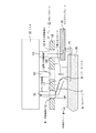
そこで、本出願人は、ケーブルでのインダクタンス増加を抑制するために種々検討した結果、その解決手法の一つを特許文献1において図7に示すプローブ装置を提案している。このプローブ装置では載置台とテスタを接続するケーブルに代えて特殊な導通機構が設けられている。そこで、このプローブ装置について図7に基づいて概説する。このプローブ装置は、図7の(a)に示すようにプローブ室1内に載置台2、プローブカード3及び導通機構4を備えている。載置台2の少なくとも上面には金等の導電性金属からなる導体膜がコレクタ電極として形成されている。載置台2の上方には複数のプローブ3Aを有するプローブカード3がカードホルダ5(同図の(b)参照)を介してプローバ室1のヘッドプレート(図示せず)に固定されている。プローブカード3の上面には複数のプローブ3Aに対応する端子電極が所定のパターンで形成され、複数のプローブ3Aがそれぞれの端子電極を介してテスタ(図示せず)と電気的に接続される。例えば、左側のプローブ3Aがパワーデバイスのゲート電極と接触し、右側のプローブ3Aがパワーデバイスのエミッタ電極と接触する。ゲート電極に電圧を印加することにより、コレクタ電極からエミッタ電極に電流が流れ、この時の電流変化(di/dt)が測定される。
Therefore, as a result of various studies to suppress an increase in inductance in the cable, the present applicant has proposed a probe apparatus shown in FIG. In this probe apparatus, a special conduction mechanism is provided in place of the cable connecting the mounting table and the tester. This probe apparatus will be outlined with reference to FIG. As shown in FIG. 7A, the probe device includes a mounting table 2, a
また、図7に示すように載置台2、プローブカード3及びカードホルダ5には載置台2の導体膜電極とテスタとを電気的に接続する導通機構4が設けられている。この導通機構4は、図7の(a)、(b)に示すように、載置台2の周面の互いに対向する位置に設けられた一対の接続端子4Bと、一対の接続端子4Bに対応して載置台2とプローブカード3の間に介在させて設けられた一対の分割導体(コンタクトプレート)4Cと、を備えている。一対の接続端子4Bは、各パワーデバイスの電気的特性を測定するために載置台2が如何なる場所へ移動してもそれぞれが対応するいずれかのコンタクトプレート4Cと弾力的に接触してコレクタ電極膜とテスタ(図示せず)とを電気的に接続する。
As shown in FIG. 7, the mounting table 2, the
図7に示すプローブ装置は上述のように導通機構4が設けられているため、パワーデバイスのスイッチング特性等の動特性を評価定する時には、載置台2のコレクタ電極膜とテスタ間の線路長が格段に短く、インダクタンスが小さいため、パワーデバイスでの電流変化を確実に測定することができる。
Since the probe device shown in FIG. 7 is provided with the
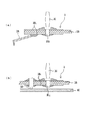
しかしながら、特許文献1には記載されていないが、現状のプローブカード3では、プローブ3Aが例えば図8の(a)に示すように回路基板3Bの配線パターン3B1、ビア導体3B2、バナナ端子等の接続プラグ3Cからなる測定用ラインを介してテスタと接続されるため、測定ライン上の抵抗が大きく抵抗にもバラツキがあり、また耐熱性も十分でないため、このようなプローブカード3をプローブ装置の実機で使用しても十分な性能を発揮できない虞がある。また、導通機構4の測定ラインも接続プラグ3C、回路基板3Bの配線パターン3B1、ビア導体3B2、ポゴピン3Dからなるため、プローブ3Aとテスタ間の測定ラインと同様の課題がある。更に、プローブカード3が複数の接続プラグ3Cを介してテスタに接続されるため、プローブカード3の着脱に大きな力を要し、例えばプローブカード3の自動交換が難しくなることもある。
However, although not described in
本発明は、上記課題を解決するためになされたもので、プローブとテスタ間の測定ラインと載置台とテスタ間の測定ラインそれぞれの抵抗を格段に低減し、プローブ装置の実機として使用しても信頼性を十分に確保することができ、容易に自動交換することができるパワーデバイス用のプローブカードを提供することを目的としている。 The present invention has been made in order to solve the above-described problems. The resistance of each of the measurement line between the probe and the tester and the measurement line between the mounting table and the tester can be greatly reduced and used as an actual device of the probe apparatus. the reliability can be sufficiently secured, and its object is to provide a probe card for a power device capable of automatically changing the easily.
本発明の請求項1に記載のプローブカードは、半導体ウエハに複数形成されたパワーデバイスの動特性を検査する際に用いられるプローブカードであって、上記パワーデバイスのエミッタ電極に電気的に接触する第1のプローブと、上記第1のプローブが接続されたブロック状の第1の接続端子と、上記パワーデバイスのゲート電極に電気的に接触する第2のプローブと、上記第2のプローブに接続されたブロック状の第2の接続端子と、上記パワーデバイスのコレクタ電極側に電気的に接触し得るコンタクトプレートと、上記コンタクトプレートに固定されたブロック状の第3の接続端子と、を備え、上記第1、第2、第3の接続端子は、それぞれが対応するテスタ側の接続端子に電気的に直に接触することを特徴とするものである。
The probe card according to
また、本発明の請求項2に記載のプローブカードは、請求項1に記載の発明において、上記第1、第2の接続端子はそれぞれ支持基板を貫通し且つ上記支持基板の両面から露出するように上記支持基板に固定され、上記コンタクトプレートは上記支持基板の上記第1、第2のプローブ側の面に固定され、上記第3の接続端子は上記支持基板に形成された孔を貫通していることを特徴とするものである。
In the probe card according to
また、本発明の請求項3に記載のプローブカードは、請求項1または請求項2に記載の発明において、上記第1、第2、第3の接続端子の上記テスタ側の面にはそれぞれ中央部が膨らむ板ばね部が形成されていることを特徴とするものである。 A probe card according to a third aspect of the present invention is the probe card according to the first or second aspect, wherein each of the first, second, and third connection terminals has a center on the tester side surface. A leaf spring part is formed, which is swelled.
また、本発明の請求項4に記載のプローブカードは、請求項3に記載の発明において、上記板ばね部は、複数の帯状部からなることを特徴とする請求項3に記載のものである。
The probe card according to
また、本発明の請求項5に記載のプローブカードは、発明において、請求項1〜請求項4のいずれか1項に記載の上記第1、第2、第3の接続端子は、それぞれ接続子を有することを特徴とするものである。
In the probe card according to
また、本発明の請求項6に記載のプローブカードは、半導体ウエハに複数形成されたパワーデバイスの動特性を検査する際に用いられるプローブカードであって、上記パワーデバイスのエミッタ電極に電気的に接触する第1のプローブと、上記パワーデバイスのゲート電極に電気的に接触する第2のプローブと、上記第1、第2のプローブがそれぞれが接続された配線パターンを有する回路基板と、上記回路基板の上記第1、第2のプローブ側の面に上記パワーデバイスのコレクタ電極側に電気的に接触し得るコンタクトプレートと、テスタに設けられ且つ上記第1、第2のプローブの配線パターンにそれぞれ電気的に接触するブロック状の第1、第2の接続端子と、上記テスタに設けられ且つ上記回路基板に形成された孔を貫通して上記コンタクトプレートに電気的に接触するブロック状の第3の接続端子と、を備えていることを特徴とするものである。 A probe card according to claim 6 of the present invention is a probe card used when inspecting dynamic characteristics of a plurality of power devices formed on a semiconductor wafer, and electrically connected to an emitter electrode of the power device. A first probe that makes contact, a second probe that makes electrical contact with the gate electrode of the power device, a circuit board having a wiring pattern to which the first and second probes are connected, and the circuit A contact plate capable of being in electrical contact with the collector electrode side of the power device on the first and second probe side surfaces of the substrate, and a wiring pattern of the first and second probes provided on the tester, respectively The block-shaped first and second connection terminals that are in electrical contact with each other and through the holes provided in the tester and formed in the circuit board. And it is characterized in that it comprises a third connection terminal block-shaped electrically contacting the tact plate, a.
本発明の請求項7に記載のプローブカードは、請求項6に記載の発明において、上記第1、第2の接続端子の上記配線パターンと接触する面にはそれぞれ中央部が膨らむ板ばね部が形成されていることを特徴とするものである。 A probe card according to a seventh aspect of the present invention is the probe card according to the sixth aspect, wherein the first and second connection terminals of the probe card have a leaf spring portion whose center portion swells on the surface in contact with the wiring pattern. It is characterized by being formed.
また、本発明の請求項8に記載のプローブカードは、請求項7に記載の発明において、上記板ばね部は、複数の帯状部からなることを特徴とするものである。 The probe card according to an eighth aspect of the present invention is the probe card according to the seventh aspect, wherein the leaf spring portion is composed of a plurality of strip-shaped portions.
また、本発明の請求項9に記載のプローブカードは、発明において、請求項6〜請求項8のいずれか1項に記載の上記第1、第2、第3の接続端子は、それぞれ接続子を有することを特徴とするものである。 In the probe card according to claim 9 of the present invention, in the invention, the first, second, and third connection terminals according to any one of claims 6 to 8 are each a connector. It is characterized by having.
本発明によれば、プローブとテスタ間の測定ラインと載置台とテスタ間の測定ラインそれぞれの抵抗を格段に低減し、プローブ装置の実機として使用しても信頼性を十分に確保することができ、容易に自動交換することができるパワーデバイス用のプローブカードを提供することができる。
According to the present invention, the resistance of the measurement line between the probe and the tester and the measurement line between the mounting table and the tester can be greatly reduced, and sufficient reliability can be secured even when used as an actual device of the probe device. , it is possible to provide a probe card for a power device capable of automatically changing the easily.
以下、図1〜図6に示す実施形態に基づいて本発明を説明する。
本実施形態のプローブカード10は、例えば図1に示すように、移動可能な載置台20の上方に配置され、載置台20上の半導体ウエハWと電気的に接触してパワーデバイスDのスイッチング特性(動特性)を評価するように構成されている。
Hereinafter, the present invention will be described based on the embodiment shown in FIGS.
For example, as shown in FIG. 1, the
本実施形態のプローブカード10は、同図に示すように、パワーデバイスDのエミッタ電極に接触する第1のプローブ11と、第1のプローブ11が接続されたブロック状の第1の接続端子12と、パワーデバイスDのゲート電極に接触する第2のプローブ13と、第2のプローブ13が接続されたブロック状の第2の接続端子14と、パワーデバイスのコレクタ電極側に接続されるコンタクトプレート15と、コンタクトプレート15の上面に固定されたブロック状の第3の接続端子16と、第1、第2のプローブ11、13を片持ち支持するプローブ支持体17と、を備え、カードホルダ30(図2の(a)、図3の(a)参照)を介してプローブ装置に装着され、第1、第2、第3の接続端子12、14、16を介してテスタ50に接続される。
As shown in the figure, the
第1のプローブ11は、図1、図2の(b)に示すように基端が第1の接続端子12の下面に接続され、先端が斜め下方に延びてプローブ支持体17によって片持ち支持され、先端がパワーデバイスDのエミッタ電極に接触するように構成されている。第1の接続端子12は、図1に示すように支持基板18に形成された第1の孔18Aを貫通した状態で支持基板18に装着され、上端面がテスタ50のエミッタ端子51と直に接触するように構成されている。
As shown in FIGS. 1 and 2B, the
第2のプローブ13及び第2の接続端子14は、いずれも図2の(b)に示すように第1のプローブ11及び第1の接続端子12と同様に構成されている。即ち、第2のプローブ13は、図1、図2の(b)に示すように基端が第2の接続端子14の下面に接続され、先端が斜め下方に延びてプローブ支持体17によって片持ち支持され、先端がパワーデバイスDのゲート電極に接触するように構成されている。第2の接続端子14は、第1の接続端子12と同様に支持基板18に形成された第2の孔18Bを貫通した状態で支持基板18に装着され、上端面がテスタ50のゲート端子52と直に接触するように構成されている。
Each of the
コンタクトプレート15は、図1に示すように載置台20の側面に付設されたコンタクトブロック21を介して載置台20の表面に形成された導体膜電極(コレクタ電極)(図示せず)に接続されるように構成されている。コンタクトブロック21は、先端部が上下方向に弾力的に揺動するように構成されている。そのため、コンタクトブロック21は、パワーデバイスDの評価時に載置台20が移動してコンタクトプレート15と弾力的に接触することにより、両者16、21間、延いてはパワーデバイスDのコレク電極とテスタ50のコレクタ端子53間で大電流が流れるように構成されている。コンタクトプレート15は、図2の(a)に示すように上下に長短の二辺を有する六角形状に形成され、支持基板18の互いに対向する両側縁部に被さるようにカードホルダ30に複数箇所で固定されている。コンタクトプレート15は、複数箇所でネジ部材を介してカードホルダ30に固定され、両者15、30の固定部にはスペーサ(図示せず)が介在し、これら両者15、30間に隙間が形成されている。コンタクトプレート15には図3の(a)に示すように支持基板18を被覆する短辺近傍に第3の接続端子16が固定されている。第3の接続端子16は、図1、図3の(b)に示すように支持基板18に形成された第3の孔18Cを貫通し、テスタ50のコレクタ端子53と直に接触するように構成されている。
The
このように第1、第2、第3の接続端子12、14、16は、ブロック状に形成されており、しかも、いずれもテスタ50のエミッタ端子51、ゲート端子52、コレクタ端子53と直に接触するため、複数の導体を経由してテスタの各端子と接続する図8のプローブカードと比較して測定ラインの抵抗が格段に小さく、大電流が流れても発熱が少ないため、大電流が流れても耐熱性が問題になることはなく、パワーデバイスDの評価の信頼性を格段に高めることができる。
As described above, the first, second, and
また、第1、第2、第3の接続端子12、14、16は、それぞれ図4、図5に示すように接続子12A、14A、16Aを有し、接続子12A、14A、16Aを介して大電流を確実に流すように構成されている。第1、第2、第3の接続端子12、14、16は、例えば銅等の良導体によって形成され、接続子12A、14A、16Aは、第1、第2、第3の接続端子12、14、16と同様に、例えば銅等の良導体によって形成されている。
Further, the first, second, and
また、第1、第2、第3の接続端子12、14、16の上面には図2の(b)、図3の(b)に示すように板ばね部12B、14B、16Bが形成され、これらの接続端子12、14、16は、板ばね部12B、14B、16Bでテスタ50のエミッタ端子51、ゲート端子52、コレクタ端子53と弾力的に接触するようになっている。そのため、第1、第2、第3の接続端子12、14、16は、テスタ50のエミッタ端子51、ゲート端子52、コレクタ端子53と電気的に確実に接続され、大電流を安定的に流すことができ、デバイス評価の信頼性を高めることができる。
Further,
これらの板ばね部12B、14B、16Bには図4の(a)、図5の(a)に示すように一定幅で複数のスリットSが切り込まれている。これらのスリットSは、板ばね部12B、14B、16Bを複数の帯状部に分割し、各帯状部に一定値の許容電流が流れるようになっている。従って、第1、第2、第3の接続端子12、14、16を流れる電流は、帯状部の本数によって所望の許容電流値に設定される。
As shown in FIGS. 4A and 5A, a plurality of slits S having a constant width are cut into the
次いで、プローブカード10の動作について説明する。本実施形態のプローブカード10は、図1に示すようにプローブ装置にカードホルダ30を介して装着して使用されると、第1、第2、第3のブロック状の接続端子12、14、16がそれぞれの板ばね部12B、14B、16Bを介してテスタ50のエミッタ端子51、ゲート端子52及びコレクタ端子53とそれぞれ弾力的且つ導通自在に接触する。
Next, the operation of the
次いで、図1に示すように複数のパワーデバイスDが形成された半導体ウエハWが載置された載置台20が移動し、アライメント機構を介してパワーデバイスDのエミッタ電極、ゲート電極と第1、第2のプローブ11、13とのアライメントが行なわれる。その後、載置台20が移動し、最初に評価すべきパワーデバイスDのエミッタ電極、ゲート電極と第1、第2のプローブ11、13とが接触する。この時、載置台20に付設されたコンタクトブロック21とコンタクトプレート15が弾力的に接触する。更に、載置台20がオーバードライブしてパワーデバイスDとテスタ50とが電気的に接続される。これにより、パワーデバイスDのエミッタ電極、ゲート電極及びコレクタ電極がテスタ50のエミッタ端子51、ゲート端子52及びコレクタ端子53との間で導通可能になる。
Next, as shown in FIG. 1, the mounting table 20 on which the semiconductor wafer W on which the plurality of power devices D are formed is moved, and the emitter electrode, the gate electrode, and the first, Alignment with the
然る後、テスタ50のゲート端子52からプローブカード10のブロック状の第2の接続端子14及び第2のプローブ13を介してパワーデバイスDのゲート電極にゲート電流を印加してターンオンすると、図1に矢印で示すようにテスタ50のコレクタ端子53からブロック状の第3の接続端子16、コンタクトプレート15、コンタクトブロック21及び載置台20の導体膜電極(コレクタ電極)を介してパワーデバイスDのコレクタ電極へ大電流(例えば、600A)が流れる。この大電流はパワーデバイスDのエミッタ電極から第1のプローブ11、ブロック状の第1の接続端子12及びエミッタ端子51を介してテスタ50へ流れ、テスタ50において測定される。このようにテスタ50からパワーデバイスDのゲート電極にゲート電圧を印加することにより、コレクタ電極からエミッタ電極に大電流を流し、電流変化を測定した後、ターンオフする。この電流変化の測定により、パワーデバイスDの動特性を確実に評価することができる。
Thereafter, when a gate current is applied to the gate electrode of the power device D from the
以上説明したように本実施形態によれば、第1、第2のプローブ11、13が接続されたブロック状の第1、第2の接続端子12、14、及びブロック状の第3の接続端子16がテスタ50のエミッタ端子51、ゲート端子52及びコレクタ端子53と直に接触するため、測定ラインの抵抗が格段に小さく、しかも耐熱性に優れており、プローブ装置のプローブカード10として十分に信頼性の高いデバイス評価を行うことができる。しかも、第1、第2、第3の接続端子12、14、16がテスタ50のエミッタ端子51、ゲート端子52及びコレクタ端子53と直に接触するため、プローブカード10の自動交換を容易に行うことができ、実用性に優れたプローブカード10を得ることができる。
As described above, according to the present embodiment, the block-shaped first and
また、本実施形態によれば、第1、第2、第3の接続端子12、14、16はそれぞれ板バネ部12B,14B、16Bを介してテスタ50と弾力的に接触するため、プローブカード10とテスタ50との間の導通性を十分に確保することができる。また、板ばね部12B,14B、16Bが複数のスリットSを介して複数の帯状部に分割されているため、帯状部の本数によって所望の電流値に設定することができる。更に、第1、第2、第3の接続端子12、14、16はそれぞれ接続子12A、14A、16Aを有するため、接続子12A、14A、16Aを介して大電流をより確実に通電することができる。
In addition, according to the present embodiment, the first, second, and
また、本発明のプローブカードは、図6に示すように構成することもできる。本実施形態のプローブカード10Aは、上記実施形態における支持基板18に代えて回路基板18’を用い、ブロック状の第1、第2、第3の接続端子12’、14’ 、16’をテスタ(図示せず)に設けた点に特徴があり、その他は上記実施形態に準じて構成されている。従って、以下では、本実施形態の特徴部分のみを説明する。
The probe card of the present invention can also be configured as shown in FIG. The
本実施形態のプローブカード10Aに用いられる回路基板18’には、図6の(a)に示すように第1、第2のプローブ11、13が接続される配線パターン18’Aが形成されている。この配線パターン18’Aは、回路基板18’の両面それぞれに所定のパターンで形成された第1、第2の配線導体18’A1、18’A2と、第1、第2の配線導体18’A1、18’A2を連結するビア導体18’A3と、で構成されている。第1、第2のプローブ11、13は、それぞれ回路基板18’の下面の第1の配線導体18’A1に例えば半田を介して接続されている。
A
また、図6の(b)に示すように回路基板18’にはテスタのコレクタ端子に対応して設けられた第3の接続端子16’が貫通するための孔18’Bが形成されている。テスタをプローブカード10Aに接続する時に、同図に示すように第3の接続端子16’が回路基板18’の孔18’Bを貫通して回路基板18’に固定されたコンタクトプレート15と板バネ部16’Aを介して弾力的に接触するようになっている。
As shown in FIG. 6B, the
本実施形態では、プローブ装置に装着されたプローブカード10Aとテスタとを接続する時には、テスタがプローブカード10Aに向けて降下すると、テスタに設けられた第1、第2の接続端子が回路基板の第1、第2のプローブ11、13に対応する配線パターの第2の配線導体に対して弾力的に接触する。第3の接続端子は、回路基板の孔を貫通してコンタクトプレート15に対して弾力的に接触する。この状態で半導体ウエハに形成された複数のパワーデバイスが評価される。本実施形態においても上記実施形態と同様の作用効果を期することができる。
In this embodiment, when connecting the
本発明は、上記実施形態に何ら制限されるものではなく、必要に応じて各構成要素を設計変更することができる。 The present invention is not limited to the above-described embodiment, and the design of each component can be changed as necessary.
10、10A プローブカード
11 第1のプローブ
12、12’ 第1のプ接続端子
12A、12’A 板ばね部
13 第2のプローブ
14、14’ 第2の接続端子
14A、14’A 板ばね部
15 コンタクトプレート
16、16’ 第3の接続端子
16A、16’A 板ばね部
18 支持基板
18’ 回路基板
18’B 孔
W 半導体ウエハ
D パワーデバイス
10,
Claims (9)
The probe card according to any one of claims 6 to 8, wherein each of the first, second, and third connection terminals has a connector.
Priority Applications (7)
| Application Number | Priority Date | Filing Date | Title |
|---|---|---|---|
| JP2011168425A JP5291157B2 (en) | 2011-08-01 | 2011-08-01 | Probe card for power devices |
| PCT/JP2012/069925 WO2013018910A1 (en) | 2011-08-01 | 2012-07-30 | Probe card for power device |
| US14/234,679 US9322844B2 (en) | 2011-08-01 | 2012-07-30 | Probe card for power device |
| EP12819684.7A EP2762897A4 (en) | 2011-08-01 | 2012-07-30 | Probe card for power device |
| KR1020147005362A KR101835680B1 (en) | 2011-08-01 | 2012-07-30 | Probe card for power device |
| CN201280037370.1A CN103703381B (en) | 2011-08-01 | 2012-07-30 | The probe card of power device |
| TW101127540A TWI541514B (en) | 2011-08-01 | 2012-07-31 | Power element with probe card |
Applications Claiming Priority (1)
| Application Number | Priority Date | Filing Date | Title |
|---|---|---|---|
| JP2011168425A JP5291157B2 (en) | 2011-08-01 | 2011-08-01 | Probe card for power devices |
Publications (3)
| Publication Number | Publication Date |
|---|---|
| JP2013032938A JP2013032938A (en) | 2013-02-14 |
| JP2013032938A5 JP2013032938A5 (en) | 2013-03-28 |
| JP5291157B2 true JP5291157B2 (en) | 2013-09-18 |
Family
ID=47629422
Family Applications (1)
| Application Number | Title | Priority Date | Filing Date |
|---|---|---|---|
| JP2011168425A Active JP5291157B2 (en) | 2011-08-01 | 2011-08-01 | Probe card for power devices |
Country Status (7)
| Country | Link |
|---|---|
| US (1) | US9322844B2 (en) |
| EP (1) | EP2762897A4 (en) |
| JP (1) | JP5291157B2 (en) |
| KR (1) | KR101835680B1 (en) |
| CN (1) | CN103703381B (en) |
| TW (1) | TWI541514B (en) |
| WO (1) | WO2013018910A1 (en) |
Families Citing this family (15)
| Publication number | Priority date | Publication date | Assignee | Title |
|---|---|---|---|---|
| JP6042760B2 (en) * | 2013-03-28 | 2016-12-14 | 東京エレクトロン株式会社 | Probe device |
| JP6042761B2 (en) * | 2013-03-28 | 2016-12-14 | 東京エレクトロン株式会社 | Probe device |
| JP5936579B2 (en) * | 2013-05-08 | 2016-06-22 | 本田技研工業株式会社 | Current application device |
| JP6045993B2 (en) * | 2013-07-08 | 2016-12-14 | 東京エレクトロン株式会社 | Probe device |
| US10527647B2 (en) * | 2013-07-09 | 2020-01-07 | Formfactor, Inc. | Probe head with inductance reducing structure |
| JP6289962B2 (en) | 2013-07-11 | 2018-03-07 | 東京エレクトロン株式会社 | Probe device |
| US10281518B2 (en) * | 2014-02-25 | 2019-05-07 | Formfactor Beaverton, Inc. | Systems and methods for on-wafer dynamic testing of electronic devices |
| US10161990B2 (en) * | 2014-03-11 | 2018-12-25 | Sintokogio, Ltd. | Inspection system for device to be tested, and method for operating inspection system for device to be tested |
| JP6218718B2 (en) * | 2014-10-22 | 2017-10-25 | 三菱電機株式会社 | Semiconductor evaluation apparatus and evaluation method thereof |
| TWI580969B (en) * | 2015-04-14 | 2017-05-01 | Mpi Corp | Probe card |
| CN106707130B (en) * | 2017-01-04 | 2019-05-03 | 株洲中车时代电气股份有限公司 | A kind of IGBT module test device |
| KR101845652B1 (en) * | 2017-01-17 | 2018-04-04 | 주식회사 텝스 | Hybrid probe card for component mounted wafer test |
| CN109298305B (en) * | 2017-07-24 | 2020-12-11 | 株洲中车时代半导体有限公司 | Testing device and method for crimping type IGBT module sub-module |
| KR102243839B1 (en) * | 2018-07-13 | 2021-04-22 | 도쿄엘렉트론가부시키가이샤 | Intermediate connection member and inspection apparatus |
| AT525517A1 (en) * | 2021-10-13 | 2023-04-15 | Gaggl Dipl Ing Dr Rainer | Test device and arrangement with this |
Family Cites Families (15)
| Publication number | Priority date | Publication date | Assignee | Title |
|---|---|---|---|---|
| JPH08184639A (en) * | 1994-12-28 | 1996-07-16 | Sony Tektronix Corp | Contactor structure |
| US7250779B2 (en) * | 2002-11-25 | 2007-07-31 | Cascade Microtech, Inc. | Probe station with low inductance path |
| JP4387125B2 (en) * | 2003-06-09 | 2009-12-16 | 東京エレクトロン株式会社 | Inspection method and inspection apparatus |
| JP4784158B2 (en) * | 2005-06-07 | 2011-10-05 | 三菱電機株式会社 | Probe card and DC characteristic measuring method using the same |
| JP2007040926A (en) | 2005-08-05 | 2007-02-15 | Tokyo Seimitsu Co Ltd | Prober |
| JP4979214B2 (en) * | 2005-08-31 | 2012-07-18 | 日本発條株式会社 | Probe card |
| JP2007123430A (en) * | 2005-10-26 | 2007-05-17 | Tokyo Seimitsu Co Ltd | Semiconductor wafer and semiconductor inspecting method |
| US7521947B2 (en) * | 2006-05-23 | 2009-04-21 | Integrated Technology Corporation | Probe needle protection method for high current probe testing of power devices |
| JP2009538428A (en) * | 2006-05-23 | 2009-11-05 | インテグレーテッド テクノロジー コーポレーション | Protecting probe needles for high current probe testing of power devices |
| US7498824B2 (en) * | 2006-08-22 | 2009-03-03 | Formfactor, Inc. | Method and apparatus for making a determination relating to resistance of probes |
| JP5016892B2 (en) * | 2006-10-17 | 2012-09-05 | 東京エレクトロン株式会社 | Inspection apparatus and inspection method |
| JP2011047782A (en) * | 2009-08-27 | 2011-03-10 | Tokyo Electron Ltd | Method for evaluating semiconductor device |
| JP5432700B2 (en) * | 2009-12-28 | 2014-03-05 | 株式会社日本マイクロニクス | Semiconductor device inspection equipment |
| JP5296117B2 (en) | 2010-03-12 | 2013-09-25 | 東京エレクトロン株式会社 | Probe device |
| CN102072974A (en) * | 2010-11-11 | 2011-05-25 | 嘉兴斯达微电子有限公司 | Clamp for power module reliability experiment |
-
2011
- 2011-08-01 JP JP2011168425A patent/JP5291157B2/en active Active
-
2012
- 2012-07-30 EP EP12819684.7A patent/EP2762897A4/en not_active Withdrawn
- 2012-07-30 CN CN201280037370.1A patent/CN103703381B/en active Active
- 2012-07-30 KR KR1020147005362A patent/KR101835680B1/en active IP Right Grant
- 2012-07-30 US US14/234,679 patent/US9322844B2/en active Active
- 2012-07-30 WO PCT/JP2012/069925 patent/WO2013018910A1/en active Application Filing
- 2012-07-31 TW TW101127540A patent/TWI541514B/en active
Also Published As
| Publication number | Publication date |
|---|---|
| TWI541514B (en) | 2016-07-11 |
| KR101835680B1 (en) | 2018-03-07 |
| KR20140057571A (en) | 2014-05-13 |
| CN103703381B (en) | 2016-12-21 |
| US9322844B2 (en) | 2016-04-26 |
| WO2013018910A1 (en) | 2013-02-07 |
| EP2762897A4 (en) | 2015-04-01 |
| JP2013032938A (en) | 2013-02-14 |
| EP2762897A1 (en) | 2014-08-06 |
| TW201326827A (en) | 2013-07-01 |
| US20140176173A1 (en) | 2014-06-26 |
| CN103703381A (en) | 2014-04-02 |
Similar Documents
| Publication | Publication Date | Title |
|---|---|---|
| JP5291157B2 (en) | Probe card for power devices | |
| JP2013032938A5 (en) | ||
| KR101389251B1 (en) | Probe apparatus | |
| US7521947B2 (en) | Probe needle protection method for high current probe testing of power devices | |
| US20020050832A1 (en) | Probe contact system having planarity adjustment mechanism | |
| EP1788401B1 (en) | Method and apparatus for testing electrical characteristics of object under test | |
| JP5432700B2 (en) | Semiconductor device inspection equipment | |
| KR101095902B1 (en) | Socket for kelvin testing | |
| JPH0955273A (en) | Ic socket for bga package ic | |
| JP2010025765A (en) | Contact structure for inspection | |
| KR102195561B1 (en) | Electrical connection device | |
| JP6000046B2 (en) | Probe unit and inspection device | |
| JP4018010B2 (en) | Semiconductor device characteristic evaluation system | |
| JP2006510026A (en) | Adapter for testing one or more conductor assemblies | |
| CN108735618A (en) | The method that device is tested and is encapsulated | |
| KR101426031B1 (en) | Apparatus of probe for kelvin test | |
| KR101183167B1 (en) | Socket for kelvin testing | |
| JP2018054401A (en) | Evaluation device and method of evaluating semiconductor device | |
| JP3172305B2 (en) | Method for manufacturing semiconductor device | |
| KR100784197B1 (en) | Probe unit | |
| JPH0618559A (en) | Probe card | |
| KR20070042612A (en) | Probe card | |
| JPH08115777A (en) | Connection apparatus | |
| JP2013105920A (en) | Measurement method of semiconductor element and probe card | |
| JPH01265531A (en) | Probe card |
Legal Events
| Date | Code | Title | Description |
|---|---|---|---|
| A521 | Request for written amendment filed |
Free format text: JAPANESE INTERMEDIATE CODE: A523 Effective date: 20121227 |
|
| A621 | Written request for application examination |
Free format text: JAPANESE INTERMEDIATE CODE: A621 Effective date: 20121227 |
|
| A871 | Explanation of circumstances concerning accelerated examination |
Free format text: JAPANESE INTERMEDIATE CODE: A871 Effective date: 20121227 |
|
| A975 | Report on accelerated examination |
Free format text: JAPANESE INTERMEDIATE CODE: A971005 Effective date: 20130208 |
|
| A131 | Notification of reasons for refusal |
Free format text: JAPANESE INTERMEDIATE CODE: A131 Effective date: 20130219 |
|
| A521 | Request for written amendment filed |
Free format text: JAPANESE INTERMEDIATE CODE: A523 Effective date: 20130419 |
|
| TRDD | Decision of grant or rejection written | ||
| A01 | Written decision to grant a patent or to grant a registration (utility model) |
Free format text: JAPANESE INTERMEDIATE CODE: A01 Effective date: 20130521 |
|
| A61 | First payment of annual fees (during grant procedure) |
Free format text: JAPANESE INTERMEDIATE CODE: A61 Effective date: 20130606 |
|
| R150 | Certificate of patent or registration of utility model |
Ref document number: 5291157 Country of ref document: JP Free format text: JAPANESE INTERMEDIATE CODE: R150 |
|
| R250 | Receipt of annual fees |
Free format text: JAPANESE INTERMEDIATE CODE: R250 |
|
| R250 | Receipt of annual fees |
Free format text: JAPANESE INTERMEDIATE CODE: R250 |
|
| R250 | Receipt of annual fees |
Free format text: JAPANESE INTERMEDIATE CODE: R250 |
|
| R250 | Receipt of annual fees |
Free format text: JAPANESE INTERMEDIATE CODE: R250 |
|
| R250 | Receipt of annual fees |
Free format text: JAPANESE INTERMEDIATE CODE: R250 |
|
| R250 | Receipt of annual fees |
Free format text: JAPANESE INTERMEDIATE CODE: R250 |
|
| R250 | Receipt of annual fees |
Free format text: JAPANESE INTERMEDIATE CODE: R250 |