JP5284412B2 - 情報記録媒体および情報記録媒体の製造方法 - Google Patents
情報記録媒体および情報記録媒体の製造方法 Download PDFInfo
- Publication number
- JP5284412B2 JP5284412B2 JP2011102950A JP2011102950A JP5284412B2 JP 5284412 B2 JP5284412 B2 JP 5284412B2 JP 2011102950 A JP2011102950 A JP 2011102950A JP 2011102950 A JP2011102950 A JP 2011102950A JP 5284412 B2 JP5284412 B2 JP 5284412B2
- Authority
- JP
- Japan
- Prior art keywords
- layer
- information
- recording medium
- recording
- information recording
- Prior art date
- Legal status (The legal status is an assumption and is not a legal conclusion. Google has not performed a legal analysis and makes no representation as to the accuracy of the status listed.)
- Expired - Fee Related
Links
Images


Classifications
-
- C—CHEMISTRY; METALLURGY
- C23—COATING METALLIC MATERIAL; COATING MATERIAL WITH METALLIC MATERIAL; CHEMICAL SURFACE TREATMENT; DIFFUSION TREATMENT OF METALLIC MATERIAL; COATING BY VACUUM EVAPORATION, BY SPUTTERING, BY ION IMPLANTATION OR BY CHEMICAL VAPOUR DEPOSITION, IN GENERAL; INHIBITING CORROSION OF METALLIC MATERIAL OR INCRUSTATION IN GENERAL
- C23C—COATING METALLIC MATERIAL; COATING MATERIAL WITH METALLIC MATERIAL; SURFACE TREATMENT OF METALLIC MATERIAL BY DIFFUSION INTO THE SURFACE, BY CHEMICAL CONVERSION OR SUBSTITUTION; COATING BY VACUUM EVAPORATION, BY SPUTTERING, BY ION IMPLANTATION OR BY CHEMICAL VAPOUR DEPOSITION, IN GENERAL
- C23C14/00—Coating by vacuum evaporation, by sputtering or by ion implantation of the coating forming material
- C23C14/22—Coating by vacuum evaporation, by sputtering or by ion implantation of the coating forming material characterised by the process of coating
- C23C14/34—Sputtering
- C23C14/3407—Cathode assembly for sputtering apparatus, e.g. Target
- C23C14/3414—Metallurgical or chemical aspects of target preparation, e.g. casting, powder metallurgy
-
- C—CHEMISTRY; METALLURGY
- C23—COATING METALLIC MATERIAL; COATING MATERIAL WITH METALLIC MATERIAL; CHEMICAL SURFACE TREATMENT; DIFFUSION TREATMENT OF METALLIC MATERIAL; COATING BY VACUUM EVAPORATION, BY SPUTTERING, BY ION IMPLANTATION OR BY CHEMICAL VAPOUR DEPOSITION, IN GENERAL; INHIBITING CORROSION OF METALLIC MATERIAL OR INCRUSTATION IN GENERAL
- C23C—COATING METALLIC MATERIAL; COATING MATERIAL WITH METALLIC MATERIAL; SURFACE TREATMENT OF METALLIC MATERIAL BY DIFFUSION INTO THE SURFACE, BY CHEMICAL CONVERSION OR SUBSTITUTION; COATING BY VACUUM EVAPORATION, BY SPUTTERING, BY ION IMPLANTATION OR BY CHEMICAL VAPOUR DEPOSITION, IN GENERAL
- C23C14/00—Coating by vacuum evaporation, by sputtering or by ion implantation of the coating forming material
- C23C14/06—Coating by vacuum evaporation, by sputtering or by ion implantation of the coating forming material characterised by the coating material
- C23C14/0623—Sulfides, selenides or tellurides
-
- G—PHYSICS
- G11—INFORMATION STORAGE
- G11B—INFORMATION STORAGE BASED ON RELATIVE MOVEMENT BETWEEN RECORD CARRIER AND TRANSDUCER
- G11B7/00—Recording or reproducing by optical means, e.g. recording using a thermal beam of optical radiation by modifying optical properties or the physical structure, reproducing using an optical beam at lower power by sensing optical properties; Record carriers therefor
- G11B7/24—Record carriers characterised by shape, structure or physical properties, or by the selection of the material
- G11B7/2403—Layers; Shape, structure or physical properties thereof
- G11B7/24035—Recording layers
- G11B7/24038—Multiple laminated recording layers
-
- G—PHYSICS
- G11—INFORMATION STORAGE
- G11B—INFORMATION STORAGE BASED ON RELATIVE MOVEMENT BETWEEN RECORD CARRIER AND TRANSDUCER
- G11B7/00—Recording or reproducing by optical means, e.g. recording using a thermal beam of optical radiation by modifying optical properties or the physical structure, reproducing using an optical beam at lower power by sensing optical properties; Record carriers therefor
- G11B7/24—Record carriers characterised by shape, structure or physical properties, or by the selection of the material
- G11B7/241—Record carriers characterised by shape, structure or physical properties, or by the selection of the material characterised by the selection of the material
- G11B7/242—Record carriers characterised by shape, structure or physical properties, or by the selection of the material characterised by the selection of the material of recording layers
- G11B7/243—Record carriers characterised by shape, structure or physical properties, or by the selection of the material characterised by the selection of the material of recording layers comprising inorganic materials only, e.g. ablative layers
- G11B7/2433—Metals or elements of Groups 13, 14, 15 or 16 of the Periodic Table, e.g. B, Si, Ge, As, Sb, Bi, Se or Te
-
- H—ELECTRICITY
- H10—SEMICONDUCTOR DEVICES; ELECTRIC SOLID-STATE DEVICES NOT OTHERWISE PROVIDED FOR
- H10N—ELECTRIC SOLID-STATE DEVICES NOT OTHERWISE PROVIDED FOR
- H10N70/00—Solid-state devices having no potential barriers, and specially adapted for rectifying, amplifying, oscillating or switching
- H10N70/011—Manufacture or treatment of multistable switching devices
- H10N70/021—Formation of switching materials, e.g. deposition of layers
- H10N70/026—Formation of switching materials, e.g. deposition of layers by physical vapor deposition, e.g. sputtering
-
- H—ELECTRICITY
- H10—SEMICONDUCTOR DEVICES; ELECTRIC SOLID-STATE DEVICES NOT OTHERWISE PROVIDED FOR
- H10N—ELECTRIC SOLID-STATE DEVICES NOT OTHERWISE PROVIDED FOR
- H10N70/00—Solid-state devices having no potential barriers, and specially adapted for rectifying, amplifying, oscillating or switching
- H10N70/20—Multistable switching devices, e.g. memristors
- H10N70/231—Multistable switching devices, e.g. memristors based on solid-state phase change, e.g. between amorphous and crystalline phases, Ovshinsky effect
-
- H—ELECTRICITY
- H10—SEMICONDUCTOR DEVICES; ELECTRIC SOLID-STATE DEVICES NOT OTHERWISE PROVIDED FOR
- H10N—ELECTRIC SOLID-STATE DEVICES NOT OTHERWISE PROVIDED FOR
- H10N70/00—Solid-state devices having no potential barriers, and specially adapted for rectifying, amplifying, oscillating or switching
- H10N70/801—Constructional details of multistable switching devices
- H10N70/821—Device geometry
- H10N70/826—Device geometry adapted for essentially vertical current flow, e.g. sandwich or pillar type devices
-
- H—ELECTRICITY
- H10—SEMICONDUCTOR DEVICES; ELECTRIC SOLID-STATE DEVICES NOT OTHERWISE PROVIDED FOR
- H10N—ELECTRIC SOLID-STATE DEVICES NOT OTHERWISE PROVIDED FOR
- H10N70/00—Solid-state devices having no potential barriers, and specially adapted for rectifying, amplifying, oscillating or switching
- H10N70/801—Constructional details of multistable switching devices
- H10N70/881—Switching materials
- H10N70/882—Compounds of sulfur, selenium or tellurium, e.g. chalcogenides
- H10N70/8828—Tellurides, e.g. GeSbTe
-
- H—ELECTRICITY
- H10—SEMICONDUCTOR DEVICES; ELECTRIC SOLID-STATE DEVICES NOT OTHERWISE PROVIDED FOR
- H10N—ELECTRIC SOLID-STATE DEVICES NOT OTHERWISE PROVIDED FOR
- H10N70/00—Solid-state devices having no potential barriers, and specially adapted for rectifying, amplifying, oscillating or switching
- H10N70/801—Constructional details of multistable switching devices
- H10N70/881—Switching materials
- H10N70/884—Switching materials based on at least one element of group IIIA, IVA or VA, e.g. elemental or compound semiconductors
-
- G—PHYSICS
- G11—INFORMATION STORAGE
- G11B—INFORMATION STORAGE BASED ON RELATIVE MOVEMENT BETWEEN RECORD CARRIER AND TRANSDUCER
- G11B11/00—Recording on or reproducing from the same record carrier wherein for these two operations the methods are covered by different main groups of groups G11B3/00 - G11B7/00 or by different subgroups of group G11B9/00; Record carriers therefor
- G11B11/002—Recording on or reproducing from the same record carrier wherein for these two operations the methods are covered by different main groups of groups G11B3/00 - G11B7/00 or by different subgroups of group G11B9/00; Record carriers therefor using recording by perturbation of the physical or electrical structure
-
- G—PHYSICS
- G11—INFORMATION STORAGE
- G11B—INFORMATION STORAGE BASED ON RELATIVE MOVEMENT BETWEEN RECORD CARRIER AND TRANSDUCER
- G11B7/00—Recording or reproducing by optical means, e.g. recording using a thermal beam of optical radiation by modifying optical properties or the physical structure, reproducing using an optical beam at lower power by sensing optical properties; Record carriers therefor
- G11B7/24—Record carriers characterised by shape, structure or physical properties, or by the selection of the material
- G11B7/241—Record carriers characterised by shape, structure or physical properties, or by the selection of the material characterised by the selection of the material
- G11B7/242—Record carriers characterised by shape, structure or physical properties, or by the selection of the material characterised by the selection of the material of recording layers
- G11B7/243—Record carriers characterised by shape, structure or physical properties, or by the selection of the material characterised by the selection of the material of recording layers comprising inorganic materials only, e.g. ablative layers
- G11B2007/24302—Metals or metalloids
- G11B2007/24312—Metals or metalloids group 14 elements (e.g. Si, Ge, Sn)
-
- G—PHYSICS
- G11—INFORMATION STORAGE
- G11B—INFORMATION STORAGE BASED ON RELATIVE MOVEMENT BETWEEN RECORD CARRIER AND TRANSDUCER
- G11B7/00—Recording or reproducing by optical means, e.g. recording using a thermal beam of optical radiation by modifying optical properties or the physical structure, reproducing using an optical beam at lower power by sensing optical properties; Record carriers therefor
- G11B7/24—Record carriers characterised by shape, structure or physical properties, or by the selection of the material
- G11B7/241—Record carriers characterised by shape, structure or physical properties, or by the selection of the material characterised by the selection of the material
- G11B7/242—Record carriers characterised by shape, structure or physical properties, or by the selection of the material characterised by the selection of the material of recording layers
- G11B7/243—Record carriers characterised by shape, structure or physical properties, or by the selection of the material characterised by the selection of the material of recording layers comprising inorganic materials only, e.g. ablative layers
- G11B2007/24302—Metals or metalloids
- G11B2007/24314—Metals or metalloids group 15 elements (e.g. Sb, Bi)
-
- G—PHYSICS
- G11—INFORMATION STORAGE
- G11B—INFORMATION STORAGE BASED ON RELATIVE MOVEMENT BETWEEN RECORD CARRIER AND TRANSDUCER
- G11B7/00—Recording or reproducing by optical means, e.g. recording using a thermal beam of optical radiation by modifying optical properties or the physical structure, reproducing using an optical beam at lower power by sensing optical properties; Record carriers therefor
- G11B7/24—Record carriers characterised by shape, structure or physical properties, or by the selection of the material
- G11B7/241—Record carriers characterised by shape, structure or physical properties, or by the selection of the material characterised by the selection of the material
- G11B7/242—Record carriers characterised by shape, structure or physical properties, or by the selection of the material characterised by the selection of the material of recording layers
- G11B7/243—Record carriers characterised by shape, structure or physical properties, or by the selection of the material characterised by the selection of the material of recording layers comprising inorganic materials only, e.g. ablative layers
- G11B2007/24302—Metals or metalloids
- G11B2007/24316—Metals or metalloids group 16 elements (i.e. chalcogenides, Se, Te)
-
- G—PHYSICS
- G11—INFORMATION STORAGE
- G11B—INFORMATION STORAGE BASED ON RELATIVE MOVEMENT BETWEEN RECORD CARRIER AND TRANSDUCER
- G11B7/00—Recording or reproducing by optical means, e.g. recording using a thermal beam of optical radiation by modifying optical properties or the physical structure, reproducing using an optical beam at lower power by sensing optical properties; Record carriers therefor
- G11B7/24—Record carriers characterised by shape, structure or physical properties, or by the selection of the material
- G11B7/241—Record carriers characterised by shape, structure or physical properties, or by the selection of the material characterised by the selection of the material
- G11B7/252—Record carriers characterised by shape, structure or physical properties, or by the selection of the material characterised by the selection of the material of layers other than recording layers
- G11B7/253—Record carriers characterised by shape, structure or physical properties, or by the selection of the material characterised by the selection of the material of layers other than recording layers of substrates
- G11B7/2533—Record carriers characterised by shape, structure or physical properties, or by the selection of the material characterised by the selection of the material of layers other than recording layers of substrates comprising resins
-
- G—PHYSICS
- G11—INFORMATION STORAGE
- G11B—INFORMATION STORAGE BASED ON RELATIVE MOVEMENT BETWEEN RECORD CARRIER AND TRANSDUCER
- G11B7/00—Recording or reproducing by optical means, e.g. recording using a thermal beam of optical radiation by modifying optical properties or the physical structure, reproducing using an optical beam at lower power by sensing optical properties; Record carriers therefor
- G11B7/24—Record carriers characterised by shape, structure or physical properties, or by the selection of the material
- G11B7/241—Record carriers characterised by shape, structure or physical properties, or by the selection of the material characterised by the selection of the material
- G11B7/252—Record carriers characterised by shape, structure or physical properties, or by the selection of the material characterised by the selection of the material of layers other than recording layers
- G11B7/257—Record carriers characterised by shape, structure or physical properties, or by the selection of the material characterised by the selection of the material of layers other than recording layers of layers having properties involved in recording or reproduction, e.g. optical interference layers or sensitising layers or dielectric layers, which are protecting the recording layers
- G11B7/2578—Record carriers characterised by shape, structure or physical properties, or by the selection of the material characterised by the selection of the material of layers other than recording layers of layers having properties involved in recording or reproduction, e.g. optical interference layers or sensitising layers or dielectric layers, which are protecting the recording layers consisting essentially of inorganic materials
-
- G—PHYSICS
- G11—INFORMATION STORAGE
- G11B—INFORMATION STORAGE BASED ON RELATIVE MOVEMENT BETWEEN RECORD CARRIER AND TRANSDUCER
- G11B7/00—Recording or reproducing by optical means, e.g. recording using a thermal beam of optical radiation by modifying optical properties or the physical structure, reproducing using an optical beam at lower power by sensing optical properties; Record carriers therefor
- G11B7/24—Record carriers characterised by shape, structure or physical properties, or by the selection of the material
- G11B7/241—Record carriers characterised by shape, structure or physical properties, or by the selection of the material characterised by the selection of the material
- G11B7/252—Record carriers characterised by shape, structure or physical properties, or by the selection of the material characterised by the selection of the material of layers other than recording layers
- G11B7/258—Record carriers characterised by shape, structure or physical properties, or by the selection of the material characterised by the selection of the material of layers other than recording layers of reflective layers
-
- G—PHYSICS
- G11—INFORMATION STORAGE
- G11C—STATIC STORES
- G11C13/00—Digital stores characterised by the use of storage elements not covered by groups G11C11/00, G11C23/00, or G11C25/00
- G11C13/0002—Digital stores characterised by the use of storage elements not covered by groups G11C11/00, G11C23/00, or G11C25/00 using resistive RAM [RRAM] elements
- G11C13/0004—Digital stores characterised by the use of storage elements not covered by groups G11C11/00, G11C23/00, or G11C25/00 using resistive RAM [RRAM] elements comprising amorphous/crystalline phase transition cells
-
- Y—GENERAL TAGGING OF NEW TECHNOLOGICAL DEVELOPMENTS; GENERAL TAGGING OF CROSS-SECTIONAL TECHNOLOGIES SPANNING OVER SEVERAL SECTIONS OF THE IPC; TECHNICAL SUBJECTS COVERED BY FORMER USPC CROSS-REFERENCE ART COLLECTIONS [XRACs] AND DIGESTS
- Y10—TECHNICAL SUBJECTS COVERED BY FORMER USPC
- Y10T—TECHNICAL SUBJECTS COVERED BY FORMER US CLASSIFICATION
- Y10T428/00—Stock material or miscellaneous articles
- Y10T428/21—Circular sheet or circular blank
Landscapes
- Chemical & Material Sciences (AREA)
- Engineering & Computer Science (AREA)
- Chemical Kinetics & Catalysis (AREA)
- Materials Engineering (AREA)
- Mechanical Engineering (AREA)
- Metallurgy (AREA)
- Organic Chemistry (AREA)
- Inorganic Chemistry (AREA)
- Manufacturing & Machinery (AREA)
- Optical Record Carriers And Manufacture Thereof (AREA)
- Thermal Transfer Or Thermal Recording In General (AREA)
- Manufacturing Optical Record Carriers (AREA)
Description
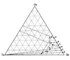
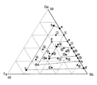
点(a)(35,65,0)、
点(b)(36.9,60,3.1)、
点(c)(3.2,60,36.8)および
点(d)(5,95,0)
で囲まれる領域内(但し、点(b)はGe60Te40−Ge35Sb65上のSb=60の点、点(c)はTe−Ge5Sb95上のSb=60の点に相当し、点(a)−点(b)、点(b)−点(c)、点(c)−点(d)および点(d)−点(a)の各ライン上を含む。)の組成を有する。
点(a)(35,65,0)、
点(b)(36.9,60,3.1)、
点(c)(3.2,60,36.8)および
点(d)(5,95,0)
で囲まれる領域内(但し、点(b)はGe60Te40−Ge35Sb65上のSb=60の点、点(c)はTe−Ge5Sb95上のSb=60の点に相当し、点(a)−点(b)、点(b)−点(c)、点(c)−点(d)および点(d)−点(a)の各ライン上を含む。)の組成を有する組成物を主成分として含む前記記録層を、前記本発明のターゲットを用いて成膜する工程を含む。
点(a)(35,65,0)、
点(b)(36.9,60,3.1)、
点(c)(3.2,60,36.8)および
点(d)(5,95,0)
で囲まれる領域内(但し、点(b)はGe60Te40−Ge35Sb65上のSb=60の点、点(c)はTe−Ge5Sb95上のSb=60の点に相当し、点(a)−点(b)、点(b)−点(c)、点(c)−点(d)および点(d)−点(a)の各ライン上を含む。)の組成を有する。
点(e)(25,75,0)、
点(f)(25,65,10)、
点(g)(7.2,65,27.8)および
点(h)(10,90,0)
で囲まれる領域内(但し、点(g)はTe−Ge10Sb90上のSb=65の点に相当し、点(e)−点(f)、点(f)−点(g)、点(g)−点(h)および点(h)−点(e)の各ライン上を含む。)の組成を有することが好ましい。このような組成物を記録層に適用することで、より高速記録に適し、再生信号品質も良好となる。
点(j)(20.9,70,9.1)、
点(k)(11.8,70,18.2)、
点(m)(14.5,85.5,0)および
点(n)(20,80,0)
で囲まれる領域内(但し、点(j)はGe50Te50−Ge14.5Sb85.5上のSb=70の点、点(k)はTe−Ge14.5Sb85.5上のSb=70の点に相当し、点(j)−点(k)、点(k)−点(m)、点(m)−点(n)および点(n)−点(j)の各ライン上を含む。)の組成を有することが、より好ましい。このような組成物を記録層に適用することで、より高速記録に適し、再生信号品質も良好となる。
点(a)(35,65,0)、
点(b)(36.9,60,3.1)、
点(c)(3.2,60,36.8)および
点(d)(5,95,0)
で囲まれる領域内(但し、点(b)はGe60Te40−Ge35Sb65上のSb=60の点、点(c)はTe−Ge5Sb95上のSb=60の点に相当し、点(a)−点(b)、点(b)−点(c)、点(c)−点(d)および点(d)−点(a)の各ライン上を含む。)の組成を有する組成物を主成分として含む。
点(a)(35,65,0)、
点(b)(36.9,60,3.1)、
点(c)(3.2,60,36.8)および
点(d)(5,95,0)
で囲まれる領域内(但し、点(b)はGe60Te40−Ge35Sb65上のSb=60の点、点(c)はTe−Ge5Sb95上のSb=60の点に相当し、点(a)−点(b)、点(b)−点(c)、点(c)−点(d)および点(d)−点(a)の各ライン上を含む。)の組成を有する組成物を主成分として含む前記記録層を、前記本発明のターゲットを用いて成膜する工程を含む。
点(e)(25,75,0)、
点(f)(25,65,10)、
点(g)(7.2,65,27.8)および
点(h)(10,90,0)
で囲まれる領域内(但し、点(g)はTe−Ge10Sb90上のSb=65の点に相当し、点(e)−点(f)、点(f)−点(g)、点(g)−点(h)および点(h)−点(e)の各ライン上を含む。)の組成を有する組成物を主成分として含む前記記録層を、前記ターゲットを用いて成膜してもよい。
点(j)(20.9,70,9.1)、
点(k)(11.8,70,18.2)、
点(m)(14.5,85.5,0)および
点(n)(20,80,0)
で囲まれる領域内(但し、点(j)はGe50Te50−Ge14.5Sb85.5上のSb=70の点、点(k)はTe−Ge14.5Sb85.5上のSb=70の点に相当し、点(j)−点(k)、点(k)−点(m)、点(m)−点(n)および点(n)−点(j)の各ライン上を含む。)の組成を有する組成物を主成分として含む前記記録層を、前記ターゲットを用いて成膜してもよい。
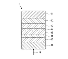
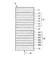
本発明の実施の形態1として、レーザ光を用いて情報の記録および再生を行う情報記録媒体の一例(本発明の第1の情報記録媒体の一例)を説明する。図2に、その光学的情報記録媒体の一部断面を示す。
点(a)(35,65,0)、
点(b)(36.9,60,3.1)、
点(c)(3.2,60,36.8)および
点(d)(5,95,0)
で囲まれる領域内(但し、点(b)はGe60Te40−Ge35Sb65上のSb=60の点、点(c)はTe−Ge5Sb95上のSb=60の点に相当し、点(a)−点(b)、点(b)−点(c)、点(c)−点(d)および点(d)−点(a)の各ライン上を含む。)の組成を有する。この範囲内の組成を適用することで、結晶化温度が高く熱的安定性があり、結晶部と非晶質部(記録部と未記録部)の間の光学変化も大きく、且つ高線速度で書換え可能な情報記録媒体を得ることができる。本実施の形態では、記録層15が実質的に上記組成物からなる場合について説明する。
点(e)(25,75,0)、
点(f)(25,65,10)、
点(g)(7.2,65,27.8)および
点(h)(10,90,0)
で囲まれる領域内(但し、点(g)はTe−Ge10Sb90上のSb=65の点に相当し、点(e)−点(f)、点(f)−点(g)、点(g)−点(h)および点(h)−点(e)の各ライン上を含む。)の組成を有することが好ましく、さらに、
点(j)(20.9,70,9.1)、
点(k)(11.8,70,18.2)、
点(m)(14.5,85.5,0)および
点(n)(20,80,0)
で囲まれる領域内(但し、点(j)はGe50Te50−Ge14.5Sb85.5上のSb=70の点、点(k)はTe−Ge14.5Sb85.5上のSb=70の点に相当し、点(j)−点(k)、点(k)−点(m)、点(m)−点(n)および点(n)−点(j)の各ライン上を含む。)の組成を有することがより好ましい。
点(a)(35,65,0)、
点(b)(36.9,60,3.1)、
点(c)(3.2,60,36.8)および
点(d)(5,95,0)
で囲まれる領域内(但し、点(b)はGe60Te40−Ge35Sb65上のSb=60の点、点(c)はTe−Ge5Sb95上のSb=60の点に相当し、点(a)−点(b)、点(b)−点(c)、点(c)−点(d)および点(d)−点(a)の各ライン上を含む。)の組成を有する組成物を主成分として含むターゲットを用いることができる。
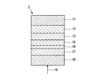
本発明の実施の形態2として、レーザ光を用いて情報の記録および再生を行う情報記録媒体のさらに別の一例(本発明の第1の情報記録媒体の別の例)を説明する。図3に、その光学的情報記録媒体の一部断面を示す。
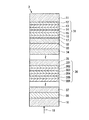
本発明の実施の形態3として、レーザ光を用いて情報の記録および再生を行う情報記録媒体のさらに別の一例(本発明の第1の情報記録媒体の別の例)を説明する。図4に、その光学的情報記録媒体の一部断面を示す。本実施の形態の情報記録媒体3は、情報を記録再生する情報層をN層(Nは2以上の整数)含んでおり、片面からのエネルギービーム(一般的には、レーザ光)19の照射により、各情報層に対して情報を記録再生できる多層光学的情報記録媒体である。情報記録媒体3には、光学分離層32、34、35、37などを介して順次情報層が積層されることによって、第1情報層31〜第N情報層38が設けられている。
本発明の実施の形態4として、レーザ光を用いて情報の記録および再生を行う情報記録媒体のさらに別の一例(本発明の第1の情報記録媒体の別の例)を説明する。図5に、その光学的情報記録媒体の一部断面を示す。本実施の形態の情報記録媒体4は、情報を記録再生する情報層を2つ(第1情報層31および第2情報層42)含んでおり、片面からのエネルギービーム(一般的には、レーザ光)19の照射により、各情報層に対して情報を記録再生できる情報記録媒体である。
本発明の実施の形態5として、レーザ光を用いて情報の記録および再生を行う情報記録媒体のさらに別の一例(本発明の第1の情報記録媒体の別の例)を説明する。図6に、その光学的情報記録媒体の一部断面を示す。
本発明の実施の形態6として、実施の形態1および2で示した情報記録媒体1または2の記録層15の異なる構成(本発明の第2の情報記録媒体の一例)について説明する。なお、便宜上、図2または図3を参照しながら、本実施の形態の情報記録媒体を説明する。
本発明の実施の形態7として、実施の形態3で示した情報記録媒体3の記録層15および304の異なる構成(本発明の第2の情報記録媒体の別の例)について説明する。なお、便宜上、図4を参照しながら、本実施の形態の情報記録媒体を説明する。
本発明の実施の形態8として、実施の形態4で示した情報記録媒体4の記録層15および404の異なる構成(本発明の第2の情報記録媒体の別の例)について説明する。なお、便宜上、図5を参照しながら、本実施の形態の情報記録媒体を説明する。
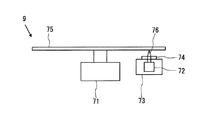
本発明の実施の形態9として、実施の形態1、2、3、4、6、7および8で説明した情報記録媒体1、2、3および4に対して、情報の記録再生を行う方法について説明する。図7に、本実施の形態の記録再生方法に用いられる記録再生装置9の一部の構成を模式的に示している。記録再生装置9は、情報記録媒体75を回転させるスピンドルモータ71と、半導体レーザ72を備える光学ヘッド73と、半導体レーザ72から出射されるレーザ光76を集光する対物レンズ74とを備える。
本発明の実施の形態10として、実施の形態5で説明した情報記録媒体5に対して、情報の記録再生を行う方法について説明する。本発明の記録再生方法に用いられる記録再生装置5の一部の構成は実施の形態9と同様であり図7に示す。ここで、実施の形態9と重複する箇所についてはその説明を省略する。
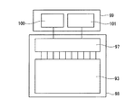
本発明の実施の形態11として、電気的エネルギーの印加による情報の記録および再生を実施する情報記録媒体の一例を示す。図8に、その電気的情報記録媒体(メモリ)86の一部断面を示す。
本発明の実施の形態12として、実施の形態11で説明した電気的情報記録媒体(メモリ)86を使用するシステムの一例を示す。図8にそのシステムの模式図を示す。
以下に、実施例を用いて本発明をさらに詳細に説明する。

本実施例では図3に示す情報記録媒体2の一例を説明する。以下、本実施例の情報記録媒体2の製造方法である。
本実施例では図4に示す情報記録媒体3の一例を説明する。本実施例では、4つの情報層を有し、第3情報層の記録層に本発明における記録層材料を適用した例(N=4、n=3)を示す。以下、本実施例の情報記録媒体3の製造方法である。
本実施例では図4に示す情報記録媒体3の一例を説明する。本実施例では、4つの情報層を有し、第4情報層の記録層に本発明における記録層材料を適用した例(N=4、n=4)を示す。以下、本実施例の情報記録媒体3の製造方法である。
本実施例では図5に示す情報記録媒体4の一例を説明する。本実施例では、第1情報層31の記録層15に本発明における記録層材料を適用した例を示す。以下、本実施例の情報記録媒体4の製造方法である。
本実施例では図5に示す情報記録媒体4の一例を説明する。本実施例では、第2情報層42の記録層404に本発明における記録層材料を適用した例を示す。以下、本実施例の情報記録媒体4の製造方法である。
本実施例では実施例6に記述の情報記録媒体4において、第2情報層42の記録層404として、Ge16Sb79Te5に対しさらに元素M(但し、MはN、Bi、C、Si、Sn、Ga、In、Zn、Cu、Ag、Au、Ni、Pd、Pt、Co、Rh、Ru、Mn、Cr、Mo、W、V、Nb、Ta、Ti、Zr、Hf、Y、La、Ce、Pr、Nd、Gd、TbおよびDyより選ばれる少なくとも1つの元素)を添加した例を示す。本実施例の情報記録媒体4の製造方法は実施例6と同様であり、記録層404の膜厚は6nmである。
本実施例では実施例6に記述の情報記録媒体4において、第2情報層42の記録層404として、Ge16Sb79Te5を適用し、第1の界面層405および第2の誘電体層403のいくつかの誘電体材料を適用した例を示す。本実施例の情報記録媒体4の製造方法は実施例6と同様である。
本実施例では図6に示す情報記録媒体5の一例を説明する。
本実施例では実施の形態6で説明した情報記録媒体(図2、3参照)の一例を説明する。以下、本実施例の情報記録媒体の製造方法について説明する。
6−103(3,4.8nm,0.5nm):Ge17Sb83(4.8nm)/Te(0.5nm)/Ge17Sb83(4.8nm)、
6−105(5,3.2nm,0.25nm):Ge17Sb83(3.2nm)/Te(0.25nm)/Ge17Sb83(3.2nm)/Te(0.25nm)/Ge17Sb83(3.2nm)。
本実施例では実施の形態7で説明した情報記録媒体(図4参照)の一例を説明する。本実施例では、4つの情報層を有する情報記録媒体において、第4情報層の記録層を実施の形態7に記載の方法で形成した例を示す。以下、本実施例の情報記録媒体の製造方法を説明する。
本実施例では実施の形態8で説明した情報記録媒体(図5参照)の一例を説明する。本実施例では、実施の形態8の情報記録媒体において、第2情報層42の記録層404を実施の形態8に記載の方法で形成した例を示す。以下、本実施例の情報記録媒体の製造方法について説明する。
本実施例では実施の形態8で説明した情報記録媒体(図5参照)の一例を説明する。本実施例では、第2情報層42の記録層404の第3構成層が、元素M(但し、MはN、Bi、C、Si、Sn、Ga、In、Zn、Cu、Ag、Au、Ni、Pd、Pt、Co、Rh、Ru、Mn、Cr、Mo、W、V、Nb、Ta、Ti、Zr、Hf、Y、La、Ce、Pr、Nd、Gd、TbおよびDyより選ばれる少なくとも1つの元素)を含む情報記録媒体を、実施の形態8に記載の方法で作製した。以下、本実施例の情報記録媒体の製造方法について説明する。
本実施例では図8に示す電気的情報記録媒体(メモリ)86の一例を説明する。
11、53、81 基板
12、302、402 反射層
13、303、403 第2の誘電体層
14、802 第2の界面層
15、304、404 記録層
16、305、405、801 第1の界面層
17、306、406 第1の誘電体層
18 カバー層
19 エネルギービーム(レーザ光)
31、33、36、38 情報層
32、34、35、37 光学分離層
301、401 透過率調整層
51 ダミー基板
52 接着層
9 記録再生装置
71 スピンドルモータ
72 半導体レーザ
73 光学ヘッド
74 対物レンズ
76 レーザ光
82 下部電極
83 第1の記録層
84 第2の記録層
85 上部電極
801 第1の界面層
802 第2の界面層
803 第3の界面層
804 第4の界面層
86、93 電気的情報記録媒体
87 印加部
88、101 抵抗測定器
89、91 スイッチ
90、100 パルス電源
92 電気的情報記録再生装置
94 ワード線
95 ビット線
96 メモリセル
97 アドレス指定回路
98 記憶装置
99 外部回路
Claims (15)
- レーザビームの照射または電流の印加によって、相変化を起こす記録層を有する情報記録媒体において、
前記記録層は、互いに接して前記記録層の厚み方向にこの順に積層された第1構成層〜第X構成層(Xは2以上の整数)によって形成されており、
前記第1構成層〜前記第X構成層には、Ge−Sbを含む層と、前記Ge−Sbを含む層とは異なる組成を有するTeを含む層とが含まれている、情報記録媒体。 - 前記第1構成層〜前記第X構成層の各膜厚dm(nm)が、0.05≦dm≦25を満たす、請求項1に記載の情報記録媒体。
- 前記第1構成層〜前記第X構成層のうち少なくとも何れか1つの構成層である第m構成層(mは1≦m≦Xを満たす正数)が、元素M(但し、Mは、N、Si、Zn、Cu、Ni、Pd、Pt、Co、Rh、Ru、Cr、Mo、W、Nb、Ta、Ti、Zr、Hf、Y、La、Ce、Pr、Nd、Gd、TbおよびDyより選ばれる少なくとも何れか1つの元素)をさらに含む、請求項1に記載の情報記録媒体。
- 前記m構成層における前記元素Mの含有量が15原子%以下である、請求項3に記載の情報記録媒体。
- 前記元素Mが、Siである、請求項3に記載の情報記録媒体。
- 前記Ge−Sbを含む層が、GepSb100-p(原子%)(pは、0<p<100を満たす)の組成式で表される材料を含む、または、前記Teを含む層が、GeqTe100-q(原子%)(qは、0≦q<100を満たす)の組成式で表される材料を含む、請求項1に記載の情報記録媒体。
- pが5≦p≦35を満たす、または、qが0≦q≦60を満たす、請求項6に記載の情報記録媒体。
- pが10≦p≦20を満たす、または、qが0≦q≦60を満たす、請求項6に記載の情報記録媒体。
- レーザビーム入射側と反対側から順に配置された第1情報層〜第N情報層を備えており、前記第1情報層〜前記第N情報層のうち少なくとも何れか1つの情報層が前記記録層を含む、請求項1に記載の情報記録媒体。
- 前記記録層に隣接して配置される第1の隣接層および第2の隣接層をさらに含み、
前記第1の隣接層および第2の隣接層の少なくとも何れか一方が、Si、Zr、Hf、Cr、In、Ga、Al、Ti、Nb、YおよびDyより選ばれる少なくとも何れか1つの元素の酸化物を含む、請求項1に記載の情報記録媒体。 - レーザビームの照射または電流の印加によって、相変化を起こす記録層を有する情報記録媒体の製造方法であって、
前記記録層は、互いに接して前記記録層の厚み方向にこの順に積層された第1構成層〜第X構成層(Xは2以上の整数)によって形成されており、前記第1構成層〜前記第X構成層には、Ge−Sbを含む層と、前記Ge−Sbを含む層とは異なる組成を有するTeを含む層とが含まれており、
前記Ge−Sbを含む層をGe−Sbを含むターゲットを用いて成膜し、前記Teを含む層を前記Ge−Sbを含むターゲットとは異なる組成を有するTeを含むターゲットを用いて成膜する工程を含む、情報記録媒体の製造方法。 - 前記ターゲットが、さらに元素M(但し、Mは、N、Si、Zn、Cu、Ni、Pd、Pt、Co、Rh、Ru、Cr、Mo、W、Nb、Ta、Ti、Zr、Hf、Y、La、Ce、Pr、Nd、Gd、TbおよびDyより選ばれる少なくとも何れか1つの元素)を含み、
前記工程において、前記ターゲットを用いて前記Ge−Sbを含む層または前記Teを含む層を成膜する、請求項11に記載の情報記録媒体の製造方法。 - 前記工程において、
前記Ge−Sbを含むターゲットを用いて、GepSb100-p(原子%)(pは、0<p<100を満たす))の組成式で表される材料を含む前記Ge−Sbを含む層を成膜する、または、前記Teを含むターゲットを用いて、GeqTe100-q(原子%)(qは、0≦q<100を満たす)の組成式で表される材料を含む前記Teを含む層を成膜する、請求項11に記載の情報記録媒体の製造方法。 - 前記情報記録媒体は、レーザビーム入射側と反対側から順に配置された第1情報層〜第N情報層を備えており、前記第1情報層〜前記第N情報層のうち少なくとも何れか1つの情報層が前記記録層を含み、
前記工程において、前記ターゲットを用いて前記記録層における前記Ge−Sbを含む層または前記Teを含む層を成膜する、請求項11に記載の情報記録媒体の製造方法。 - 前記情報記録媒体は、前記記録層に隣接して配置される第1の隣接層および第2の隣接層をさらに含んでおり、
前記第1の隣接層および前記第2の隣接層の少なくとも何れか一方を、Si、Zr、Hf、Cr、In、Ga、Al、Ti、Nb、YおよびDyより選ばれる少なくとも何れか1つの元素の酸化物を含むターゲットを用いて成膜する工程をさらに含む、請求項11に記載の情報記録媒体の製造方法。
Priority Applications (1)
| Application Number | Priority Date | Filing Date | Title |
|---|---|---|---|
| JP2011102950A JP5284412B2 (ja) | 2006-11-01 | 2011-05-02 | 情報記録媒体および情報記録媒体の製造方法 |
Applications Claiming Priority (3)
| Application Number | Priority Date | Filing Date | Title |
|---|---|---|---|
| JP2006297387 | 2006-11-01 | ||
| JP2006297387 | 2006-11-01 | ||
| JP2011102950A JP5284412B2 (ja) | 2006-11-01 | 2011-05-02 | 情報記録媒体および情報記録媒体の製造方法 |
Related Parent Applications (1)
| Application Number | Title | Priority Date | Filing Date |
|---|---|---|---|
| JP2007284401A Division JP4964093B2 (ja) | 2006-11-01 | 2007-10-31 | 情報記録媒体、並びに、ターゲットおよびそれを用いた情報記録媒体の製造方法 |
Publications (2)
| Publication Number | Publication Date |
|---|---|
| JP2011154781A JP2011154781A (ja) | 2011-08-11 |
| JP5284412B2 true JP5284412B2 (ja) | 2013-09-11 |
Family
ID=41316449
Family Applications (1)
| Application Number | Title | Priority Date | Filing Date |
|---|---|---|---|
| JP2011102950A Expired - Fee Related JP5284412B2 (ja) | 2006-11-01 | 2011-05-02 | 情報記録媒体および情報記録媒体の製造方法 |
Country Status (2)
| Country | Link |
|---|---|
| US (1) | US8017208B2 (ja) |
| JP (1) | JP5284412B2 (ja) |
Families Citing this family (9)
| Publication number | Priority date | Publication date | Assignee | Title |
|---|---|---|---|---|
| JPWO2006112165A1 (ja) * | 2005-04-07 | 2008-12-04 | 松下電器産業株式会社 | 光学的情報記録媒体とその製造方法 |
| JPWO2010041373A1 (ja) * | 2008-10-06 | 2012-03-01 | パナソニック株式会社 | 情報記録媒体とその製造方法、及びスパッタリングターゲット |
| CN101981620A (zh) * | 2008-11-26 | 2011-02-23 | 松下电器产业株式会社 | 信息记录介质、记录装置、再现装置以及再现方法 |
| US8437235B2 (en) * | 2008-12-16 | 2013-05-07 | Panasonic Corporation | Optical information recording medium and recording/reproducing method therefor |
| TWI402829B (zh) * | 2010-10-29 | 2013-07-21 | Nat Univ Tsing Hua | 多階記錄方法及其系統 |
| TWI426511B (zh) * | 2011-03-31 | 2014-02-11 | Cmc Magnetics Corp | 可寫錄光記錄媒體 |
| US9770688B2 (en) * | 2015-10-22 | 2017-09-26 | King Fahd University Of Petroleum And Minerals | Si—Y nanocomposite membrane and methods of making and use thereof |
| CN109585649B (zh) * | 2018-10-30 | 2019-12-27 | 同济大学 | 类超晶格锗锑/锌锑纳米相变薄膜及其制备和应用 |
| FR3092200B1 (fr) * | 2019-01-28 | 2021-10-22 | Commissariat Energie Atomique | Memoire resistive a changement de phase |
Family Cites Families (11)
| Publication number | Priority date | Publication date | Assignee | Title |
|---|---|---|---|---|
| JPH0832482B2 (ja) | 1986-09-22 | 1996-03-29 | 松下電器産業株式会社 | 光学的情報記録媒体 |
| JP3365653B2 (ja) | 1993-07-13 | 2003-01-14 | 住友ゴム工業株式会社 | 空気入りタイヤ |
| JP2001028148A (ja) * | 1999-05-12 | 2001-01-30 | Matsushita Electric Ind Co Ltd | 光学的情報記録媒体とその製造方法、記録再生方法及び記録再生装置 |
| US6365256B1 (en) * | 2000-02-29 | 2002-04-02 | Eastman Kodak Company | Erasable phase change optical recording elements |
| WO2004008447A1 (en) * | 2002-07-15 | 2004-01-22 | Koninklijke Philips Electronics N.V. | Multi-stack optical data storage medium and use of such medium |
| JP4252867B2 (ja) | 2002-09-06 | 2009-04-08 | 三菱化学メディア株式会社 | 光学的情報記録媒体 |
| US7439007B2 (en) * | 2002-12-20 | 2008-10-21 | Ricoh Company, Ltd. | Phase change information recording medium having multiple layers and recording and playback method for the medium |
| JP4181490B2 (ja) * | 2003-03-25 | 2008-11-12 | 松下電器産業株式会社 | 情報記録媒体とその製造方法 |
| DE602004031775D1 (de) * | 2004-02-05 | 2011-04-21 | Ricoh Co Ltd | Phasenänderungsinformationsaufzeichnungsmedium, verfahren zu dessen herstellung und sputtertarget. |
| US7485356B2 (en) * | 2004-07-15 | 2009-02-03 | Tdk Corporation | Optical recording medium |
| CN101194310B (zh) * | 2005-06-07 | 2011-03-02 | 松下电器产业株式会社 | 信息记录介质及其制造方法 |
-
2007
- 2007-10-31 US US11/931,160 patent/US8017208B2/en not_active Expired - Fee Related
-
2011
- 2011-05-02 JP JP2011102950A patent/JP5284412B2/ja not_active Expired - Fee Related
Also Published As
| Publication number | Publication date |
|---|---|
| JP2011154781A (ja) | 2011-08-11 |
| US20090286037A1 (en) | 2009-11-19 |
| US8017208B2 (en) | 2011-09-13 |
Similar Documents
| Publication | Publication Date | Title |
|---|---|---|
| JP5284412B2 (ja) | 情報記録媒体および情報記録媒体の製造方法 | |
| KR101011581B1 (ko) | 정보 기록 매체와 그 제조 방법 | |
| KR100671253B1 (ko) | 정보 기록 매체와 그 제조 방법 | |
| JP4217213B2 (ja) | 情報記録媒体とその製造方法 | |
| JP5100846B2 (ja) | 情報記録媒体とその製造方法、およびスパッタリングターゲット | |
| KR20060043831A (ko) | 정보 기록 매체 및 이를 제조하기 위한 방법 | |
| KR100634138B1 (ko) | 정보 기록 매체 및 그 제조 방법 | |
| JP4567750B2 (ja) | 情報記録媒体とその製造方法 | |
| KR20050120639A (ko) | 정보기록 매체 및 그 제조 방법 | |
| JPWO2011024381A1 (ja) | 情報記録媒体とその製造方法 | |
| JP2005056545A (ja) | 情報記録媒体とその製造方法 | |
| JP4964093B2 (ja) | 情報記録媒体、並びに、ターゲットおよびそれを用いた情報記録媒体の製造方法 | |
| JP4593617B2 (ja) | 情報記録媒体とその製造方法 | |
| JP4308160B2 (ja) | 情報記録媒体とその製造方法 | |
| JP4871733B2 (ja) | 情報記録媒体とその製造方法 | |
| JP4308741B2 (ja) | 情報記録媒体及びその製造方法 | |
| JP5226537B2 (ja) | 情報記録媒体およびその製造方法、スパッタリングターゲットならびに成膜装置 | |
| US8580368B2 (en) | Information recording medium and method for manufacturing the same | |
| JPWO2007063672A1 (ja) | 情報記録媒体とその製造方法 | |
| JPWO2006109534A1 (ja) | 情報記録媒体とその製造方法 | |
| JPWO2006057116A1 (ja) | 情報記録媒体とその製造方法 |
Legal Events
| Date | Code | Title | Description |
|---|---|---|---|
| A621 | Written request for application examination |
Free format text: JAPANESE INTERMEDIATE CODE: A621 Effective date: 20110502 |
|
| A977 | Report on retrieval |
Free format text: JAPANESE INTERMEDIATE CODE: A971007 Effective date: 20120614 |
|
| A131 | Notification of reasons for refusal |
Free format text: JAPANESE INTERMEDIATE CODE: A131 Effective date: 20120710 |
|
| A521 | Request for written amendment filed |
Free format text: JAPANESE INTERMEDIATE CODE: A523 Effective date: 20120906 |
|
| TRDD | Decision of grant or rejection written | ||
| A01 | Written decision to grant a patent or to grant a registration (utility model) |
Free format text: JAPANESE INTERMEDIATE CODE: A01 Effective date: 20130507 |
|
| A61 | First payment of annual fees (during grant procedure) |
Free format text: JAPANESE INTERMEDIATE CODE: A61 Effective date: 20130529 |
|
| R150 | Certificate of patent or registration of utility model |
Ref document number: 5284412 Country of ref document: JP Free format text: JAPANESE INTERMEDIATE CODE: R150 |
|
| LAPS | Cancellation because of no payment of annual fees |