JP5269741B2 - Electronic component package and detection device - Google Patents
Electronic component package and detection device Download PDFInfo
- Publication number
- JP5269741B2 JP5269741B2 JP2009240077A JP2009240077A JP5269741B2 JP 5269741 B2 JP5269741 B2 JP 5269741B2 JP 2009240077 A JP2009240077 A JP 2009240077A JP 2009240077 A JP2009240077 A JP 2009240077A JP 5269741 B2 JP5269741 B2 JP 5269741B2
- Authority
- JP
- Japan
- Prior art keywords
- pad
- mounting
- electronic component
- notch
- package
- Prior art date
- Legal status (The legal status is an assumption and is not a legal conclusion. Google has not performed a legal analysis and makes no representation as to the accuracy of the status listed.)
- Active
Links
Images


Classifications
-
- G—PHYSICS
- G01—MEASURING; TESTING
- G01P—MEASURING LINEAR OR ANGULAR SPEED, ACCELERATION, DECELERATION, OR SHOCK; INDICATING PRESENCE, ABSENCE, OR DIRECTION, OF MOVEMENT
- G01P1/00—Details of instruments
- G01P1/02—Housings
- G01P1/023—Housings for acceleration measuring devices
-
- B—PERFORMING OPERATIONS; TRANSPORTING
- B81—MICROSTRUCTURAL TECHNOLOGY
- B81B—MICROSTRUCTURAL DEVICES OR SYSTEMS, e.g. MICROMECHANICAL DEVICES
- B81B7/00—Microstructural systems; Auxiliary parts of microstructural devices or systems
- B81B7/0032—Packages or encapsulation
- B81B7/0074—3D packaging, i.e. encapsulation containing one or several MEMS devices arranged in planes non-parallel to the mounting board
-
- G—PHYSICS
- G01—MEASURING; TESTING
- G01D—MEASURING NOT SPECIALLY ADAPTED FOR A SPECIFIC VARIABLE; ARRANGEMENTS FOR MEASURING TWO OR MORE VARIABLES NOT COVERED IN A SINGLE OTHER SUBCLASS; TARIFF METERING APPARATUS; MEASURING OR TESTING NOT OTHERWISE PROVIDED FOR
- G01D11/00—Component parts of measuring arrangements not specially adapted for a specific variable
- G01D11/24—Housings ; Casings for instruments
- G01D11/245—Housings for sensors
-
- B—PERFORMING OPERATIONS; TRANSPORTING
- B81—MICROSTRUCTURAL TECHNOLOGY
- B81B—MICROSTRUCTURAL DEVICES OR SYSTEMS, e.g. MICROMECHANICAL DEVICES
- B81B2201/00—Specific applications of microelectromechanical systems
- B81B2201/02—Sensors
- B81B2201/0228—Inertial sensors
- B81B2201/0235—Accelerometers
-
- H—ELECTRICITY
- H01—ELECTRIC ELEMENTS
- H01L—SEMICONDUCTOR DEVICES NOT COVERED BY CLASS H10
- H01L2224/00—Indexing scheme for arrangements for connecting or disconnecting semiconductor or solid-state bodies and methods related thereto as covered by H01L24/00
- H01L2224/01—Means for bonding being attached to, or being formed on, the surface to be connected, e.g. chip-to-package, die-attach, "first-level" interconnects; Manufacturing methods related thereto
- H01L2224/02—Bonding areas; Manufacturing methods related thereto
- H01L2224/04—Structure, shape, material or disposition of the bonding areas prior to the connecting process
- H01L2224/05—Structure, shape, material or disposition of the bonding areas prior to the connecting process of an individual bonding area
- H01L2224/05001—Internal layers
- H01L2224/05005—Structure
- H01L2224/05009—Bonding area integrally formed with a via connection of the semiconductor or solid-state body
-
- H—ELECTRICITY
- H01—ELECTRIC ELEMENTS
- H01L—SEMICONDUCTOR DEVICES NOT COVERED BY CLASS H10
- H01L2224/00—Indexing scheme for arrangements for connecting or disconnecting semiconductor or solid-state bodies and methods related thereto as covered by H01L24/00
- H01L2224/01—Means for bonding being attached to, or being formed on, the surface to be connected, e.g. chip-to-package, die-attach, "first-level" interconnects; Manufacturing methods related thereto
- H01L2224/02—Bonding areas; Manufacturing methods related thereto
- H01L2224/04—Structure, shape, material or disposition of the bonding areas prior to the connecting process
- H01L2224/05—Structure, shape, material or disposition of the bonding areas prior to the connecting process of an individual bonding area
- H01L2224/0554—External layer
- H01L2224/05541—Structure
- H01L2224/05548—Bonding area integrally formed with a redistribution layer on the semiconductor or solid-state body
-
- H—ELECTRICITY
- H01—ELECTRIC ELEMENTS
- H01L—SEMICONDUCTOR DEVICES NOT COVERED BY CLASS H10
- H01L2224/00—Indexing scheme for arrangements for connecting or disconnecting semiconductor or solid-state bodies and methods related thereto as covered by H01L24/00
- H01L2224/01—Means for bonding being attached to, or being formed on, the surface to be connected, e.g. chip-to-package, die-attach, "first-level" interconnects; Manufacturing methods related thereto
- H01L2224/02—Bonding areas; Manufacturing methods related thereto
- H01L2224/04—Structure, shape, material or disposition of the bonding areas prior to the connecting process
- H01L2224/05—Structure, shape, material or disposition of the bonding areas prior to the connecting process of an individual bonding area
- H01L2224/0554—External layer
- H01L2224/0556—Disposition
- H01L2224/05568—Disposition the whole external layer protruding from the surface
-
- H—ELECTRICITY
- H01—ELECTRIC ELEMENTS
- H01L—SEMICONDUCTOR DEVICES NOT COVERED BY CLASS H10
- H01L2224/00—Indexing scheme for arrangements for connecting or disconnecting semiconductor or solid-state bodies and methods related thereto as covered by H01L24/00
- H01L2224/01—Means for bonding being attached to, or being formed on, the surface to be connected, e.g. chip-to-package, die-attach, "first-level" interconnects; Manufacturing methods related thereto
- H01L2224/02—Bonding areas; Manufacturing methods related thereto
- H01L2224/04—Structure, shape, material or disposition of the bonding areas prior to the connecting process
- H01L2224/05—Structure, shape, material or disposition of the bonding areas prior to the connecting process of an individual bonding area
- H01L2224/0554—External layer
- H01L2224/0556—Disposition
- H01L2224/0557—Disposition the external layer being disposed on a via connection of the semiconductor or solid-state body
-
- H—ELECTRICITY
- H01—ELECTRIC ELEMENTS
- H01L—SEMICONDUCTOR DEVICES NOT COVERED BY CLASS H10
- H01L2224/00—Indexing scheme for arrangements for connecting or disconnecting semiconductor or solid-state bodies and methods related thereto as covered by H01L24/00
- H01L2224/01—Means for bonding being attached to, or being formed on, the surface to be connected, e.g. chip-to-package, die-attach, "first-level" interconnects; Manufacturing methods related thereto
- H01L2224/10—Bump connectors; Manufacturing methods related thereto
- H01L2224/15—Structure, shape, material or disposition of the bump connectors after the connecting process
- H01L2224/16—Structure, shape, material or disposition of the bump connectors after the connecting process of an individual bump connector
- H01L2224/161—Disposition
- H01L2224/16151—Disposition the bump connector connecting between a semiconductor or solid-state body and an item not being a semiconductor or solid-state body, e.g. chip-to-substrate, chip-to-passive
- H01L2224/16221—Disposition the bump connector connecting between a semiconductor or solid-state body and an item not being a semiconductor or solid-state body, e.g. chip-to-substrate, chip-to-passive the body and the item being stacked
- H01L2224/16225—Disposition the bump connector connecting between a semiconductor or solid-state body and an item not being a semiconductor or solid-state body, e.g. chip-to-substrate, chip-to-passive the body and the item being stacked the item being non-metallic, e.g. insulating substrate with or without metallisation
- H01L2224/16235—Disposition the bump connector connecting between a semiconductor or solid-state body and an item not being a semiconductor or solid-state body, e.g. chip-to-substrate, chip-to-passive the body and the item being stacked the item being non-metallic, e.g. insulating substrate with or without metallisation the bump connector connecting to a via metallisation of the item
-
- H—ELECTRICITY
- H01—ELECTRIC ELEMENTS
- H01L—SEMICONDUCTOR DEVICES NOT COVERED BY CLASS H10
- H01L2924/00—Indexing scheme for arrangements or methods for connecting or disconnecting semiconductor or solid-state bodies as covered by H01L24/00
- H01L2924/0001—Technical content checked by a classifier
- H01L2924/00014—Technical content checked by a classifier the subject-matter covered by the group, the symbol of which is combined with the symbol of this group, being disclosed without further technical details
-
- H—ELECTRICITY
- H01—ELECTRIC ELEMENTS
- H01L—SEMICONDUCTOR DEVICES NOT COVERED BY CLASS H10
- H01L2924/00—Indexing scheme for arrangements or methods for connecting or disconnecting semiconductor or solid-state bodies as covered by H01L24/00
- H01L2924/01—Chemical elements
- H01L2924/01078—Platinum [Pt]
-
- H—ELECTRICITY
- H01—ELECTRIC ELEMENTS
- H01L—SEMICONDUCTOR DEVICES NOT COVERED BY CLASS H10
- H01L2924/00—Indexing scheme for arrangements or methods for connecting or disconnecting semiconductor or solid-state bodies as covered by H01L24/00
- H01L2924/01—Chemical elements
- H01L2924/01079—Gold [Au]
-
- H—ELECTRICITY
- H01—ELECTRIC ELEMENTS
- H01L—SEMICONDUCTOR DEVICES NOT COVERED BY CLASS H10
- H01L2924/00—Indexing scheme for arrangements or methods for connecting or disconnecting semiconductor or solid-state bodies as covered by H01L24/00
- H01L2924/095—Indexing scheme for arrangements or methods for connecting or disconnecting semiconductor or solid-state bodies as covered by H01L24/00 with a principal constituent of the material being a combination of two or more materials provided in the groups H01L2924/013 - H01L2924/0715
- H01L2924/097—Glass-ceramics, e.g. devitrified glass
- H01L2924/09701—Low temperature co-fired ceramic [LTCC]
-
- H—ELECTRICITY
- H01—ELECTRIC ELEMENTS
- H01L—SEMICONDUCTOR DEVICES NOT COVERED BY CLASS H10
- H01L2924/00—Indexing scheme for arrangements or methods for connecting or disconnecting semiconductor or solid-state bodies as covered by H01L24/00
- H01L2924/10—Details of semiconductor or other solid state devices to be connected
- H01L2924/146—Mixed devices
- H01L2924/1461—MEMS
-
- H—ELECTRICITY
- H01—ELECTRIC ELEMENTS
- H01L—SEMICONDUCTOR DEVICES NOT COVERED BY CLASS H10
- H01L2924/00—Indexing scheme for arrangements or methods for connecting or disconnecting semiconductor or solid-state bodies as covered by H01L24/00
- H01L2924/15—Details of package parts other than the semiconductor or other solid state devices to be connected
- H01L2924/151—Die mounting substrate
- H01L2924/1515—Shape
- H01L2924/15153—Shape the die mounting substrate comprising a recess for hosting the device
- H01L2924/15155—Shape the die mounting substrate comprising a recess for hosting the device the shape of the recess being other than a cuboid
- H01L2924/15156—Side view
-
- H—ELECTRICITY
- H01—ELECTRIC ELEMENTS
- H01L—SEMICONDUCTOR DEVICES NOT COVERED BY CLASS H10
- H01L2924/00—Indexing scheme for arrangements or methods for connecting or disconnecting semiconductor or solid-state bodies as covered by H01L24/00
- H01L2924/15—Details of package parts other than the semiconductor or other solid state devices to be connected
- H01L2924/151—Die mounting substrate
- H01L2924/153—Connection portion
-
- H—ELECTRICITY
- H01—ELECTRIC ELEMENTS
- H01L—SEMICONDUCTOR DEVICES NOT COVERED BY CLASS H10
- H01L2924/00—Indexing scheme for arrangements or methods for connecting or disconnecting semiconductor or solid-state bodies as covered by H01L24/00
- H01L2924/19—Details of hybrid assemblies other than the semiconductor or other solid state devices to be connected
- H01L2924/1901—Structure
- H01L2924/1904—Component type
- H01L2924/19041—Component type being a capacitor
Abstract
Description
本発明は電子部品用パッケージ及び検出装置に関する。 The present invention relates to an electronic component package及beauty detection apparatus.
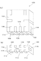
加速度等を検出する検出素子等の電子部品が搭載された基板状のパッケージが、その端面が実装基板側の実装面に直角に当接して実装される電子部品用パッケージについては、例えば下記特許文献1に記載されている。
特許文献1に記載されている電子部品用パッケージを構成するパッケージ本体の概略を図10(a)(b)に示す。図10に示す基板状のパッケージ本体100は、複数のセラミック板を積層して形成されたパッケージであって、電子部品としてMEMS(Micro Electro Mechanical System)が搭載されている。
このパッケージ本体100が垂直実装される端面102は、図10(a)に示す様に、端面102と交差する第1側面104に形成されたリード端子106,106・・の各々から延出されたリード端子108が形成されている。
更に、図10(b)に示す様に、第1側面104に対して反対面となる第2側面110に形成されたリード端子112,112・・の各々からも、端面102にリード端子114が延出されている。
また、図10に示すパッケージ本体100のリード端子106,112が形成された側面と異なる側面には、端面102を実装基板の実装面に当接してパッケージ本体100を直角に実装する際に、パッケージ本体100の実装基板に対する固着強度を補強すべく、はんだ接続される金属層116,116が形成されている。
For a package for an electronic component in which an electronic component such as a detection element for detecting acceleration or the like is mounted and the end surface of the package is mounted at right angles to the mounting surface on the mounting substrate side, for example, the following
The outline of the package main body which comprises the package for electronic components described in
The
Further, as shown in FIG. 10B,
Further, when the
図10に示すパッケージ本体100を実装基板の実装面に直角に実装する際には、端面102を実装基板の実装面に当接して、端面102に形成されたリード端子108,114の各々を実装基板の実装面に形成された対応するパッドに当接すると共に、パッケージ本体100の金属層116,116の各々を実装基板の対応するパッドに当接する。次いで、リード端子108,114の各々と対応する実装基板のパッド、及び金属層116,116の各々と対応する実装基板のパッドとをはんだ接続する。
しかし、図10に示すパッケージ本体100は、複数のセラミック板を積層し焼成して形成されたパッケージであるため、幅狭の端面102を平坦面に形成することは困難である。このため、実装基板の実装面に端面102を当接したとき、パッケージ本体100と実装基板の実装面との角度が不確定である。
この様に、パッケージ本体100と実装基板の実装面との角度が不確定な加速度等の検知装置では、搭載されたMEMSによる検知精度が著しく低下し、検知装置として使用できないおそれがある。
従って、パッケージ本体100と実装基板の実装面との角度が一定角度で立設されているように特別な配慮を払う必要がある。
そこで、本発明の課題は、実装基板に実装したとき、実装基板の実装面との角度が不確定状態となるおそれのある従来の電子部品用パッケージの課題を解決し、実装基板の実装面に、実装面との角度を所定角度で確実に実装できる電子部品用パッケージ及び検知装置を提供することを目的とする。
When the
However, since the
As described above, in a detection device such as an acceleration in which the angle between the
Therefore, it is necessary to pay special attention so that the angle between the
Therefore, the problem of the present invention is to solve the problem of the conventional electronic component package, in which the angle with the mounting surface of the mounting substrate may be indeterminate when mounted on the mounting substrate. , and to provide an electronic component package及beauty biopsy known apparatus that can reliably implement a predetermined angle the angle between the mounting surface.
本発明者等は、前記課題を解決すべく検討した結果、実装基板の平坦な実装面に当接する基板状のパッケージ本体の端面を平坦な切断面に形成し、且つパッケージ本体の切断面と側面との境界部に形成した切欠部の内壁面に、パッケージ本体に搭載した電子部品の電極端子と電気的に接続されたパッドを形成し、この切欠部内にはんだを充填することによって、切欠部内のパッドと実装基板の実装面に形成したパッドとを電気的に接合できると共に、パッケージ本体を実装基板の実装面に容易に所定角度で実装できることを知った。
すなわち、本発明者等は、前記課題を解決する手段として、第1側面およびこの反対面となる第2側面と前記第1および第2側面に交差する端面とを含む基板状のパッケージ本体に、電子部品が搭載された電子部品用パッケージであって、前記端面が実装基板側の平坦な実装面に当接して、前記パッケージ本体が前記実装面に対して直角に固着して実装されるように、前記端面が平坦な切断面に形成され、前記端面と前記第1側面との境界部には、第1切欠部が形成され、前記端面と前記第2側面との境界部には、第2切欠部が形成され、前記第1切欠部の内壁面には、前記第1側面との交差角が鈍角となる傾斜面が前記第1切欠部の側壁面の全てに形成され、前記第2切欠部の内壁面には、前記第2側面との交差角が鈍角となる傾斜面が前記第2切欠部の側壁面の全てに形成され、前記第1切欠部の傾斜面には、前記実装面に対する固着用の第1パッドが形成され、前記第2切欠部の傾斜面には、前記実装面に対する固着用の第2パッドが形成され、前記第1および第2パッドのうち、一方が前記電子部品と電気的に接続されている接続パッドであり、他方が前記電子部品と電気的に接続されていないダミーパッドである電子部品用パッケージを提供できる。
As a result of studying to solve the above problems, the present inventors have formed the end surface of the substrate-like package body that contacts the flat mounting surface of the mounting substrate into a flat cutting surface, and the cutting surface and side surfaces of the package body. A pad electrically connected to the electrode terminal of the electronic component mounted on the package body is formed on the inner wall surface of the notch formed at the boundary with the solder, and the inside of the notch is filled with solder. It has been found that the pad and the pad formed on the mounting surface of the mounting substrate can be electrically bonded, and the package body can be easily mounted on the mounting surface of the mounting substrate at a predetermined angle.
That is, the present inventors, as means for solving the above problems, in a substrate-like package body including a first side surface and a second side surface opposite to the first side surface and an end surface intersecting the first and second side surfaces, An electronic component package on which an electronic component is mounted, wherein the end surface is in contact with a flat mounting surface on the mounting substrate side, and the package body is fixed and mounted at a right angle to the mounting surface. The end surface is formed as a flat cut surface, a first notch is formed at a boundary portion between the end surface and the first side surface, and a second portion is formed at a boundary portion between the end surface and the second side surface. A notch portion is formed, and an inclined surface having an obtuse angle with the first side surface is formed on the inner wall surface of the first notch portion on all side wall surfaces of the first notch portion, and the second notch The inner wall surface of the part has an inclined surface with an obtuse angle with the second side surface. A first pad for fixing to the mounting surface is formed on the inclined surface of the first notch, and the inclined surface of the second notch is formed on the inclined surface of the second notch. A second pad for fixing to the mounting surface is formed, and one of the first and second pads is a connection pad electrically connected to the electronic component, and the other is electrically connected to the electronic component. It is possible to provide an electronic component package that is a dummy pad that is not connected .
パッケージ本体の端面を、実装基板側の平坦な実装面に直角に当接して実装することによって、電子部品用パッケージを実装基板側の実装面に確実に直角に実装できる。
また、切欠部の内壁面に形成した傾斜面にパッドを形成することによって、パッドを容易に形成でき、電子部品の電極端子から延出された配線パターンとも容易に接続できる。
更に、パッケージ本体に、切断面と交差する第1側面との境界部に第1切欠部と、前記第1側面に対して反対面となる第2側面と切断面との境界部に第2切欠部とを形成し、前記第1切欠部と第2切欠部との一方に形成したパッドを電子部品と電気的に接続することによって、第1切欠部と第2切欠部との各々にはんだを充填したとき、各切欠部内に充填した溶融はんだの収縮に起因して発生する電子部品用パッケージの傾斜を防止できる。
かかる第1切欠部及び第2切欠部の各々の内壁面に形成した傾斜面にパッドを形成することによって、内壁面にパッドが形成された第1切欠部と同程度の溶融はんだとの濡れ性を呈する。このため、第1切欠部及び第2切欠部内に充填された溶融はんだの表面張力によるメニスカスも同程度のものが形成される。このパッドも、第2切欠部の傾斜面に形成することによって、容易に形成できる。
The end surface of the package body, by implementing in right angle contact with the flat mounting surface of the mounting substrate, an electronic component package reliably perpendicularly mounted on a mounting surface of the mounting substrate side.
Moreover, by forming a pad on the inclined surface formed on the inner wall surface of the notch, the pad can be easily formed and can be easily connected to a wiring pattern extended from the electrode terminal of the electronic component.
Furthermore, the package body has a first notch at a boundary portion between the first side surface intersecting the cut surface, and a second notch at a boundary portion between the second side surface and the cut surface opposite to the first side surface. And electrically connecting a pad formed on one of the first notch and the second notch to an electronic component, thereby soldering each of the first notch and the second notch. When filled, it is possible to prevent the electronic component package from being inclined due to the shrinkage of the molten solder filled in each notch.
By forming a pad on the inclined surface formed on the inner wall surface of each of the first notch part and the second notch part, the wettability with the molten solder equivalent to the first notch part on which the pad is formed on the inner wall surface. Presents. For this reason, the same meniscus is formed by the surface tension of the molten solder filled in the first notch and the second notch. This pad can also be easily formed by forming it on the inclined surface of the second notch.
かかる本発明者等が提供した課題を解決する手段において、下記の好ましい態様を上げることができる。In the means for solving the problems provided by the present inventors, the following preferred embodiments can be raised.
前記第2側面には、電子部品搭載用の凹部が形成され、前記凹部内には、前記電子部品が接合される接合パッドが形成され、前記接合パッドが、前記接続パッドと電気的に接続され、前記電子部品が、前記接合パッドと接合して該接合パッドを介して前記接続パッドと電気的に接続され、前記凹部内で搭載されている。A concave portion for mounting an electronic component is formed on the second side surface, a bonding pad to which the electronic component is bonded is formed in the concave portion, and the bonding pad is electrically connected to the connection pad. The electronic component is bonded to the bonding pad, electrically connected to the connection pad via the bonding pad, and mounted in the recess.
また、前記凹部内には、該凹部の底面から突出する突出部が形成され、前記接合パッドが、前記突出部の先端面に形成され、前記電子部品が、前記突出部の先端面で搭載されて、前記凹部の底面から離間している。In addition, a protrusion that protrudes from the bottom surface of the recess is formed in the recess, the bonding pad is formed on the tip surface of the protrusion, and the electronic component is mounted on the tip surface of the protrusion. And spaced from the bottom surface of the recess.
また、前記第1切欠部内から前記第1側面上に引き出されるように前記第1パッドを含む第1配線が形成され、前記第2切欠部内から前記第2側面上に引き出されるように前記第2パッドを含む第2配線が形成されている。Also, a first wiring including the first pad is formed so as to be drawn out from the first cutout portion onto the first side surface, and the second wiring is drawn out from the second cutout portion onto the second side surface. A second wiring including a pad is formed.
また、前記第2配線が、前記第2切欠部内から前記第2側面上に引き出されて、更に、前記凹部の内壁面に沿って形成されている。The second wiring is formed on the second side surface from the second notch and further along the inner wall surface of the recess.
また、前記パッケージ本体には、前記第1側面から前記第2側面にかけて貫通するヴィアが形成され、前記ヴィアが、前記接続パッドと電気的に接続されている。The package main body is formed with a via penetrating from the first side surface to the second side surface, and the via is electrically connected to the connection pad.
また、前記第1パッドが、前記第1切欠部の内壁面のうち、前記端面側を除いた領域の全面に形成され、前記第2パッドが、前記第2切欠部の内壁面のうち、前記端面側を除いた領域の全面に形成されている。The first pad is formed on the entire surface of the inner wall surface of the first cutout portion except for the end face side, and the second pad is formed of the inner wall surface of the second cutout portion. It is formed on the entire surface excluding the end face side.
また、前記第1側面上には、前記第1パッドを露出して第1ソルダーレジストが形成され、前記第2側面上には、前記第2パッドを露出して第2ソルダーレジストが形成されている。Further, a first solder resist is formed on the first side surface by exposing the first pad, and a second solder resist is formed on the second side surface by exposing the second pad. Yes.
更に、本発明者等は、前記課題を解決する手段として、前記電子部品用パッケージが、前記実装面に実装されている検出装置において、前記電子部品が、検出素子であり、前記実装面には、前記パッケージ本体に対する固着用の第3および第4パッドが形成され、前記第1切欠部に充填された第1はんだによって前記第1パッドと前記第3パッドとが電気的に接続され、かつ、前記第2切欠部に充填された第2はんだによって前記第2パッドと前記第4パッドとが電気的に接続されて、前記端面が前記実装面に当接して、前記実装面に前記パッケージ本体が固着されている検出装置を提供できる。
パッケージ本体の端面を、実装基板側の平坦な実装面に直角に当接して実装することによって、電子部品用パッケージを実装基板側の実装面に確実に直角に実装でき、検出素子の検出精度の向上を図ることができる。
また、パッケージ本体の切欠部の内壁面に形成された傾斜面にパッドを形成することによって、切欠部の内壁面にパッドを容易に形成でき、検知素子の電極端子から延出された配線パターンとも容易に接続できる。
更に、パッケージ本体に、切断面と交差する第1側面との境界部に第1切欠部と、前記第1側面に対して反対面となる第2側面と切断面との境界部に第2切欠部とを形成すると共に、前記第1切欠部及び第2切欠部の一方に形成したパッドを検出素子と電気的に接続し、且つ前記切断面が実装基板側の実装面に当接して、前記実装面に対して装着したパッケージ本体を固着するように、前記第1切欠部及び第2切欠部内にはんだを充填することによって、各切欠部内に充填した溶融はんだの収縮に起因して発生するパッケージ本体の傾斜を防止できる。この第1切欠部及び第2切欠部の各々の内壁面に形成したパッドによって、第1切欠部及び第2切欠部の内壁面は溶融はんだに対して良好な濡れ性を呈する。このため、第1切欠部及び第2切欠部内に充填された溶融はんだの表面張力によって良好なメニスカスを形成できる。このパッドも、第1切欠部及び第2切欠部の各々に形成した傾斜面に形成することによって、容易に形成できる。
かかる本発明者等が提供した課題を解決する手段では、実装基板側に設けた実装面を、実装基板の一面側に配設した中継基板に形成することによって、実装基板の表面が凹凸面に形成されていても、パッケージ本体を搭載する中継基板の搭載面を平坦面に形成できる。この中継基板としては、シリコン基板又はセラミック基板によって形成することが好ましい。
Furthermore, the present inventors have, as means for solving the above-mentioned problems, in the detection device in which the electronic component package is mounted on the mounting surface, the electronic component is a detection element, and the mounting surface has Third and fourth pads for fixing to the package body are formed, and the first pad and the third pad are electrically connected by the first solder filled in the first notch, and The second pad and the fourth pad are electrically connected by the second solder filled in the second notch, the end surface abuts the mounting surface, and the package body is on the mounting surface. A fixed detection device can be provided .
The end surface of the package body, by implementing in right angle contact with the flat mounting surface of the mounting board side, can be reliably right angle mounting electronic component package on a mounting surface of the mounting board side, the detection accuracy of the detection element Can be improved.
Further, by forming a pad on the inclined surface formed on the inner wall surface of the cutout portion of the package body, the pad can be easily formed on the inner wall surface of the cutout portion, and a wiring pattern extending from the electrode terminal of the detection element Easy to connect.
Furthermore, the package body has a first notch at a boundary portion between the first side surface intersecting the cut surface, and a second notch at a boundary portion between the second side surface and the cut surface opposite to the first side surface. A pad formed on one of the first notch and the second notch is electrically connected to the detection element, and the cut surface is in contact with the mounting surface on the mounting substrate side, A package generated due to shrinkage of the molten solder filled in each notch by filling the first notch and the second notch with solder so that the package body attached to the mounting surface is fixed. The inclination of the main body can be prevented. Due to the pads formed on the inner wall surfaces of the first notch portion and the second notch portion, the inner wall surfaces of the first notch portion and the second notch portion exhibit good wettability with respect to the molten solder. For this reason, a favorable meniscus can be formed by the surface tension of the molten solder filled in the first notch and the second notch. This pad can also be easily formed by forming it on the inclined surface formed in each of the first notch and the second notch.
In the means for solving the problems provided by the present inventors, the mounting surface provided on the mounting substrate side is formed on a relay substrate disposed on one surface side of the mounting substrate, so that the surface of the mounting substrate becomes an uneven surface. Even if formed, the mounting surface of the relay substrate on which the package body is mounted can be formed as a flat surface. The relay substrate is preferably formed of a silicon substrate or a ceramic substrate.
本発明者等が提供した電子部品用パッケージでは、実装基板側の実装面に当接する、基板状のパッケージ本体の端面が、平坦な切断面によって形成されている。
更に、パッケージ本体の切断面と交差する第1側面との境界部に形成した切欠部の内壁面に、電子部品の電極端子と電気的に接続されたパッドが形成され、実装基板側の実装面と当接する切断面にパッドを形成することを要しない。
このため、電子部品用パッケージを形成するパッケージ本体の切断面を実装基板側の実装面に当接することによって、電子部品用パッケージを実施基板側の実装面に容易に所定角度で確実に装着できる。
また、実装基板側の実装面に所定角度で装着した電子部品用パッケージの切欠部内にはんだを充填することによって、実装基板側の実装面に装着された電子部品用パッケージを固着すると共に、実装基板側の実装面に形成したパッドとパッケージ本体に搭載した電子部品と電気的に接続されたパッドとを電気的に接続できる。
その結果、実装基板側の実装面に電子部品用パッケージを実装する際に、電子部品用パッケージを実装基板側の実装面に対して容易に所定角度で確実に装着でき、切欠部に充填するはんだによって電子部品用パッケージと実装基板とを電気的に接続し且つ固着できる。
In the electronic component package provided by the present inventors, the end surface of the substrate-like package body that comes into contact with the mounting surface on the mounting substrate side is formed by a flat cut surface.
Furthermore, a pad electrically connected to the electrode terminal of the electronic component is formed on the inner wall surface of the notch formed at the boundary between the cut surface of the package body and the first side surface intersecting the mounting surface on the mounting substrate side. It is not necessary to form a pad on the cut surface that comes into contact with.
For this reason, the electronic component package can be easily and surely attached to the mounting surface on the implementation substrate side at a predetermined angle by bringing the cut surface of the package body forming the electronic component package into contact with the mounting surface on the mounting substrate side.
In addition, the electronic component package mounted on the mounting surface on the mounting substrate side is fixed by filling the notch portion of the electronic component package mounted on the mounting surface on the mounting substrate side at a predetermined angle. The pads formed on the side mounting surface and the pads electrically connected to the electronic components mounted on the package body can be electrically connected.
As a result, when mounting the electronic component package on the mounting surface on the mounting board side, the electronic component package can be easily and securely attached to the mounting surface on the mounting board side at a predetermined angle, and the solder filling the notch Thus, the electronic component package and the mounting substrate can be electrically connected and fixed.
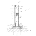
本発明者等が提供した検知装置の一例を図1に示す。図1に示す検知装置では、電子部品としての加速度等を検知する検知素子が、電子部品用パッケージであるセンサ用パッケージPに搭載されている。
かかるセンサ用パッケージPは、実装基板12の一面側に中継基板14を介して搭載されている。この中継基板14は、一面側がセンサ用パッケージPの実装面14aに形成されていると共に、他面側が実装基板12と接続される接続面に形成されている。かかる中継基板14の実装面14aは、平坦な水平面に形成されている。
この様な、中継基板14の実装面14aには、センサ用パッケージPを形成する基板状のパッケージ本体10の端面10cが当接し、センサ用パッケージPが中継基板14の実装面14aに対して直角に実装(垂直実装)されている。
かかるパッケージ本体10の端面10cは、平坦な切断面に形成されており、センサ用パッケージPは中継基板14にはんだ16,16によって固着されている。
この中継基板14は、図2に示す様に、平板状のシリコン基板18の一面側(実装面14a)に形成されたパッド20,20が、シリコン基板18の一面側に形成された配線パターン22,22及びシリコン基板18を貫通するヴィア24を経由してシリコン基板18の他面側(接続面)に形成されたパッド26,26に電気的に接続されている。これらの配線パターン22,22及びパッド20,20が、パッケージ本体10との接続に必要な個所を除いてソルダーレジスト23によって覆われている。
かかるシリコン基板18の他面側に形成されたパッド26,26は、図1に示す様に、実装基板12の表面に形成されたパッド28,28にはんだ30,30によって接続されている。
この様に、実装基板12の一面側に中継基板14を配設することによって、実装基板12の表面が凹凸面に形成されていても、パッケージ本体10を搭載する中継基板14の実装面14aを平坦面に形成できる。
尚、シリコン基板18には、シリコン基板18の一面側に研磨を施して平坦面とした後に、パッド20や配線パターン22を形成することが好ましい。
An example of a detection device provided by the present inventors is shown in FIG. In the detection apparatus shown in FIG. 1, a detection element that detects acceleration or the like as an electronic component is mounted on a sensor package P that is an electronic component package.
The sensor package P is mounted on one surface side of the mounting substrate 12 via the
The end surface 10c of the substrate-
The end surface 10c of the
As shown in FIG. 2, the
The
In this manner, by disposing the
In addition, it is preferable to form the
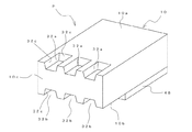
図1に示すセンサ用パッケージPの斜視図を図3に示す。図3に示すパッケージ本体10は、略長方形状であって、平板状のシリコン基板34によって形成されている。シリコン基板34には、第1側面10aと第1側面10aに対向する第2側面10b(図1に示すセンサ用パッケージPにおいて、蓋体48が装着された面に相当)とが形成されていると共に、この第1側面10a及び第2側面10bと直交する端面10cが形成されている。端面10cは、第1側面10a及び第2側面10bよりも小面積である。
かかる端面10cは、中継基板14の実装面14aに当接する当接面であって、端面10cと直交する第1側面10aとの境界部には、図3に示す様に、第1切欠部32a,32a,32aが形成されている。かかる第1切欠部32aは、第1側面10aと端面10cとに開口され、第1切欠部32aの側壁面は第1側面10aとの交差角が鈍角となる傾斜面32c,32c,32cに形成されている。
更に、図3に示す様に、第1側面10aに対して反対側面には、端面10cと直交する第2側面10bが形成されている。この第2側面10bと端面10cとの境界部にも、第2切欠部32b,32b,32bが形成されている。この第2切欠部32bは、第2側面10bと端面10cとに開口され、第2切欠部32bの側壁面は第2側面10bとの交差角が鈍角となる傾斜面32c,32c,32cに形成されている。
このため、パッケージ本体10の端面10cの外周は、図3に示す様に、第1切欠部32a,32a,32a及び第2切欠部32b,32b,32bによって、凹凸形状となっているが、端面10cは平坦面である。
尚、図3においては、パッケージ本体10の形状を説明するため、配線パターン等については図示を省略した。
A perspective view of the sensor package P shown in FIG. 1 is shown in FIG. The
The end surface 10c is an abutting surface that abuts on the mounting surface 14a of the
Further, as shown in FIG. 3, a
For this reason, as shown in FIG. 3, the outer periphery of the end surface 10c of the
In FIG. 3, the wiring pattern and the like are not shown in order to explain the shape of the
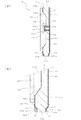
図3に示すセンサ用パッケージPの縦断面図を図4(a)に示し、その部分拡大図を図4(b)に示す。
センサ用パッケージPを形成するパッケージ本体10のシリコン基板34の図3に示す第2側面10bには、図4に示す様に、搭載用凹部36が形成されている。この搭載用凹部36の底面から突出する突出部39の先端面は、MEMS等の検知素子38が搭載される搭載面に形成されている。
かかるシリコン基板34の第1側面10a及び第2側面10bの全表面には、SiO2から成る絶縁層34aによって被覆されている。この「全表面」には、搭載用凹部36の内壁面、突出部39の表面、第1切欠部32a,32a,32a及び第2切欠部32b,32b,32bの内壁面、及び後述するヴィア40を形成するヴィア穴41の内壁面を含む。
FIG. 4A shows a longitudinal sectional view of the sensor package P shown in FIG. 3, and FIG. 4B shows a partially enlarged view thereof.
As shown in FIG. 4, a mounting
The entire surface of the first side surface 10a and the
搭載用凹部36の底面から突出する突出部39の先端面には、検知素子38の各電極端子と接続されるパッド40a,40aが絶縁層34a上に形成されている。かかるパッド40a,40aは、シリコン基板34を貫通するヴィア40,40及びシリコン基板34の第1側面10a(図3)の絶縁層34a上に形成された配線パターン42を経由して、第1切欠部32aの内壁面の絶縁層34a上に形成されたパッド44に電気的に接続されている。このため、パッケージ本体10の端面10cには、パッド等を形成することがなく、平坦面を保持できる。
かかるパッド44は、端面10cとの交差縁近傍を除く第1切欠部32aの内壁面の全面に形成することが好ましいが、少なくとも第1切欠部32aの傾斜面32cに形成されていればよい。特に、第1切欠部32aの端面10cに開口する開口部に対向する傾斜面32cにパッド44が形成されていることが好ましい。このパッド44は、第1側面10a上に延出されていてもよい。
パッケージ本体10の第1側面10aに形成された配線パターン42・・は、パッド44を除いてソルダーレジスト50によって被覆されている。このパッド44も、その端面10cとの交差縁近傍の部分は、ソルダーレジスト50によって被覆されている。
シリコン基板34の搭載用凹部36内に搭載された検知素子38は、搭載用凹部36の開口部を覆う蓋体48によって封止されている。この蓋体48は、シリコン基板34に接着剤48aによって貼着されている。
また、パッケージ本体10に形成された第2切欠部32b,32b,32bの各内壁面にも、図4に示す様に、銅等の金属から成るダミーパッド46が形成されている。かかるダミーパッド46は、端面10cとの交差縁近傍を除く第2切欠部32bの内壁面の全面に形成することが好ましいが、少なくとも第2切欠部32bの傾斜面32cに形成されていればよい。特に、第2切欠部32bの端面10cに開口する開口部に対向する傾斜面32cにダミーパッド46が形成されていることが好ましい。このダミーパッド46は、第2側面10b上に延出されていてもよい。
パッケージ本体10の第2側面10bに形成されたダミーパッド46のうち、第2側面10bに形成された部分は、ソルダーレジスト50によって被覆され、ダミーパッド46の端面10cとの交差縁近傍の部分も、ソルダーレジスト50によって被覆されている。
尚、搭載用凹部36内には、MEMS等の検知素子38と共に、半導体素子やキャパシタ等の受動部品を同時に搭載してもよい。
Pads 40a, 40a connected to the respective electrode terminals of the
The pad 44 is preferably formed on the entire inner wall surface of the first cutout portion 32a except for the vicinity of the crossing edge with the end face 10c, but may be formed at least on the inclined surface 32c of the first cutout portion 32a. In particular, it is preferable that the pad 44 is formed on the inclined surface 32c that faces the opening that opens in the end surface 10c of the first notch 32a. The pad 44 may extend on the first side surface 10a.
The
The
Further, as shown in FIG. 4,
Of the
In the mounting
かかるセンサ用パッケージPは、図5に示す方法によって製造できる。図5では、図1に示すパッケージ本体10の第2側面10b側を上方に向けた状態で示している。
先ず、図5(a)に示す様に、板状体としての平板状のシリコン板52の両面側にケミカルエッチングを施して、シリコン板52の一面側に、検知素子38を搭載する複数の搭載用凹部36,36を所定間隔で形成し、且つシリコン基板52の他面側で搭載用凹部36,36の中間部に相当する部分に第1切欠部用凹部31aを形成すると共に、第1切欠部用凹部31aに対応して搭載用凹部36,36の中間部に第2切欠凹部31bを形成する。搭載用凹部36,第1切欠部用凹部31a及び第2切欠用凹部31bの形状は、シリコン板52の一面側又は他面側に開口される開口部が底面よりも幅広となる逆台形状である。
尚、このケミカルエッチングは、シリコン板52の両面側の所定箇所がエッチングされるように、シリコン基板52の両面側にエッチング用レジストによるマスクを被着して施す。
Such a sensor package P can be manufactured by the method shown in FIG. FIG. 5 shows the
First, as shown in FIG. 5A, chemical etching is performed on both sides of a
The chemical etching is performed by applying a mask made of an etching resist on both sides of the
更に、図5(b)に示す様に、ドライエッチングによって、各搭載用凹部36,36の検知素子38を搭載する搭載面にヴィア穴41,41を形成する。かかるドライエッチングも、シリコン板52の所定箇所がエッチングされるように、シリコン基板52の両面側にエッチング用レジストによるマスクを被着して施す。
このドライエッチングの際に、ヴィア穴41,41を形成した部分を除く搭載用凹部36の底面を掘り込み、ヴィア穴41,41を形成した部分を搭載用凹部36の底面から突出した突出部39に形成する。
この突出部39に、後述する様に、検知素子38を搭載することによって、検知素子38を搭載用凹部36の底面から離間状態にでき、検知素子38による検出精度を向上できる。
かかる搭載用凹部36,36及びヴィア穴41,41を形成したシリコン板52に熱酸化処理を施して、図5(c)に示す様に、ヴィア穴41,41の内壁面を含むシリコン板52の全表面にSiO2から成る絶縁層34aを形成する。
尚、ヴィア穴41,41の内壁面を含むシリコン板52の全表面に、CVDやスパッタによってSiNやSiO2から成る膜を形成して絶縁層34aとしてもよく、エポキシやポリイミド等の絶縁樹脂の塗布等の方法によって絶縁層34aを形成してもよい。
Further, as shown in FIG. 5B, via
During this dry etching, the bottom surface of the mounting
As will be described later, by mounting the
The
A film made of SiN or SiO 2 may be formed by CVD or sputtering on the entire surface of the
次いで、図5(d)に示す様に、ヴィア穴41,41内に金属を充填してヴィア40,40を形成すると共に、ヴィア40,40から延出した配線パターン42,42を第1切欠部用凹部31aに向けて延出し、第1切欠部用凹部31aの内壁面にパッド44を形成する。更に、第2切欠部用凹部31bの内壁面にダミーパッド46を形成する。
かかるパッド44及びダミーパッド46には、はんだ16との濡れ性向上のために、ニッケルめっき層から成る下地めっき層が形成され、更にその上に金めっき層が形成されている。
また、ヴィア40,40の突出部39の上端面には、搭載される検知素子38の電極端子と接合されるパッド40a,40aが形成されている。パッド40a,40a上には、検知素子38の電極端子との接合性を向上すべく、ニッケルめっき層から成る下地めっき層が形成され、更にその上に金めっき層が形成されている。
かかるヴィア40,40、パッド40a,40a、配線パターン42、パッド44及びダミーパッド46は、銅めっきによって形成できる。例えば、ヴィア穴41,41の内壁面を含むシリコン板52の全表面に、無電解銅めっき或いはスパッタ等によって薄膜銅層を形成した後、感光性レジストによってパターニングを施し、次いで、薄膜銅層を給電層とする電解銅めっきを施して、ヴィア穴41,41内に銅を充填しつつ、パッド40a,40a、配線パターン42、パッド44及びダミーパッド46としての銅層を形成できる。その後、感光性レジストを剥離して露出した薄膜銅層をエッチングして除去することによって、ヴィア40,40、パッド40a,40a、配線パターン42、パッド44及びダミーパッド46としての銅層の間の絶縁を図ることができる。
この様にして形成したヴィア40,40の搭載用凹部36側の端部には、搭載される検知素子38の電極端子と接合されるパッド40a,40aが形成されている。
更に、パッド40a,40a、パッド44及びダミーパッド46には、検知素子38の電極端子との接合性やはんだ16との濡れ性の向上を図るべく、ニッケルめっき層から成る下地めっき層を形成し、更にその上に金めっき層を形成する。
その後、シリコン板52の他面側に形成した配線パターン42、第1切欠部用凹部31a及び第2切欠用凹部31bの各底面の中央部を、ソルダーレジスト50によって被覆する。
Next, as shown in FIG. 5D, the via holes 41 and 41 are filled with metal to form the
In order to improve wettability with the
In addition, pads 40 a and 40 a that are joined to the electrode terminals of the mounted
The
Pads 40a and 40a to be joined to the electrode terminals of the mounted
Furthermore, a base plating layer made of a nickel plating layer is formed on the pads 40a, 40a, the pad 44, and the
Thereafter, the solder resist 50 covers the center portions of the bottom surfaces of the
更に、図5(e)に示す様に、搭載用凹部36,36の各々に検知素子38を搭載する。この際に、検知素子38の各電極端子は、対応するパッド40a、ヴィア40及び配線パターン42を経由して第1切欠部用凹部31aの内壁面に露出するパッド44に電気的に接続される。
検知素子38が搭載された搭載用凹部36,36の各開口部には、図5(f)に示す様に、蓋体48が被着されて検知素子38は封止される。
その後、図5(f)の一点鎖線で示す位置でシリコン板52をダイシングブレードで切断してセンサ用パッケージP,Pを得る。この際に、第1切欠部用凹部31a及び第2切欠部用凹部31bの各底面の中央部に形成したソルダレジスト50の中央でシリコン板52を切断する。
この様に、シリコン板52を第1切欠部用凹部31a及び第2切欠部用凹部31bの各底面の中央部で切断して形成した切断面は平坦面であって、この切断面を端面10cとする図4に示すセンサ用パッケージPを得ることができる。
この蓋体48としては、シリコン板やガラス板を用いることができる。かかるシリコン板やガラス板を蓋体48として用いる場合、蓋体48とシリコン基板34とを、陽極接合によって接合することができる。かかる陽極接合では、接着剤を不要にでき、搭載用凹部36を高度の気密状態とすることができる。この様な高度な気密状態は、検知素子38の検知精度を向上する上で好ましい。
尚、図5では、搭載用凹部36,36の各々に搭載した検知素子38を封止した後に切断していたが、図5(d)の工程でヴィア40,40、パッド40a,40a、配線パターン42、パッド44及びダミーパッド46を形成した後、シリコン板52を切断して得た各個片のパッケージ本体10の搭載用凹部36に検知素子38を搭載し、次いで搭載用凹部36を蓋体48によって封止してセンサー用パッケージPを得てもよい。
Further, as shown in FIG. 5 (e), a
As shown in FIG. 5 (f), a
Thereafter, the
Thus, the cut surface formed by cutting the
As the
In FIG. 5, the
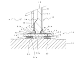
得られた図4に示すセンサ用パッケージPを実装する際には、図6に示す様に、センサ用パッケージPを形成するパッケージ本体10の端面10cである切断面(以下、単に切断面10cと称することがある)を、中継基板14の実装面14aに近接する。
かかる中継基板14のパッド26,26は、実装基板12に形成されたパッド28,28にはんだ30によって接合されている。このため、実装基板12のパッド28,28の形成面が凹凸面であって、パッド28,28の表面高さに差異が存在していても、かかる差異は、はんだ30によって吸収でき、中継基板14の実装面14aを水平面となるように調整できる。
この中継基板14の実装面14aに形成されたパッド20,20上には、はんだ16,16が載置されている。
かかるはんだ16は、センサ用パッケージPの切断面10cが、中継基板14の実装面14aに当接したとき、溶融されて、図7に示す様に、パッケージ本体10の第1切欠部32aの内壁面に形成されたパッド44と接触し、その表面張力によって第1切欠部32a内に充填されてメニスカスを形成する。この様にして第1切欠部32a内に充填されたはんだ16は、中継基板14のパッド20とセンサ用パッケージPのパッド44とを電気的に接続すると共に、センサ用パッケージPを中継基板14の実装面14aに対して直角に固着する。
また、図7に示す様に、センサ用パッケージPの切断面10cが、中継基板14の実装面14aに当接したとき、溶融されたはんだ16が、パッケージ本体10の第2切欠部32bの内壁面に形成されたダミーパッド46と接触し、その表面張力によって第2切欠部32b内に充填されてメニスカスを形成する。この様にして第2切欠部32b内に充填されたはんだ16は、中継基板14の実装面に対してセンサ用パッケージPを直角に固着する(垂直実装)。
かかる第1切欠部32a及び第2切欠部32bの内壁面である傾斜面32cに、パッド44やダミーパッド46を形成しているため、センサ用パッケージPを中継基板14に実装する際に、第1切欠部32a及び第2切欠部32b内にはんだが充填されたとき、良好なメニスカスが形成され、センサ用パッケージPを中継基板14の実装面14aに対して正確に直角に実装できる。
このパッド44やダミーパッド46によってはんだ16との濡れ性を向上でき、第1切欠部32a及び第2切欠部32b内からはんだ16が流出し、隣接するパッド44とのショートを惹起することを防止できる。
更に、第1切欠部32a及び第2切欠部32b内に充填された溶融はんだ16が凝固するとき、その収縮力を互いに打ち消してセンサ用パッケージPの傾斜を防止できる。
When the obtained sensor package P shown in FIG. 4 is mounted, as shown in FIG. 6, a cut surface (hereinafter simply referred to as a cut surface 10c) which is an end surface 10c of the
The
On the
The
Further, as shown in FIG. 7, when the cut surface 10 c of the sensor package P contacts the mounting surface 14 a of the
Since the pad 44 and the
The pad 44 and the
Further, when the
この様に、実装基板12上に設けた中継基板14の水平面に形成された実装面14aに対して、検知素子38が搭載されたセンサ用パッケージPを直角に装着(垂直実装)した検知装置は、自動車、携帯電話器その他の電子装置に用い、加速度、角速度、傾斜等を検出できる。特に、センサ用パッケージPを直角に実装している検知装置は、方向性を精度よく検出できる。
また、複数のセンサ用パッケージP,P・・を装着できる中継基板14を実装基板12上に配設することによって、実装基板12上に高密度にセンサ用パッケージP,P・・を装着した検知装置を提供できる。
図1〜図7に示すセンサ用パッケージPでは、パッケージ本体10の第1切欠部32a内に検知素子38と電気的に接続されたパッド44を形成し、第2切欠部32b内にダミーパッド46を形成していたが、図8に示す様に、第2切欠部32b内に形成したパッド44とパッケージ本体10の搭載用凹部36の底面に搭載された検出素子38の電極端子とを、搭載用凹部36の内壁面に沿って第2側面10b上に引き出されるように形成した配線パターン42によって電気的に接続してもよい。
この様に、搭載用凹部36の内壁面に沿って形成した配線パターン42に検出素子38を搭載することによって、ヴィア40,40の形成を不要にでき、センサ用パッケージPの構造を簡素化できる。
図8に示すセンサ用パッケージPのパッケージ本体10の第1切欠部32a内には、ダミーパッド46が形成されている。
尚、図1に示すセンサ用パッケージPと図8に示すセンサ用パッケージPとを組み合わせて、パッケージ本体10の第1切欠部32a及び第2切欠部32bの両方に、検出素子38の電極端子と電気的に接続されたパッド44を形成してもよい。
In this way, the detection device in which the sensor package P on which the
Further, by disposing the
In the sensor package P shown in FIGS. 1 to 7, a pad 44 electrically connected to the
Thus, by mounting the
A
The sensor package P shown in FIG. 1 and the sensor package P shown in FIG. 8 are combined, and the electrode terminal of the
ここまで説明したセンサ用パッケージPのパッケージ本体10では、第1側面10aと第2側面10bとに第1切欠部32aと第2切欠部32bとを対向して形成していたが、第1切欠部32aと第2切欠部32bとに充填されたはんだ16,16の張力が、互いに打ち消し合うことができればよく、第1切欠部32aと第2切欠部32bとを千鳥状に形成してもよい。更に、ダミーパッド46が設けられた第1切欠部32a,32a・・とパッド44が設けられた第2切欠部32b,32b・・との一方のみが形成されていてもよい。
また、パッケージ本体10の搭載用凹部36の底面に、ヴィア40,40から配線パターンを引き出して、この配線パターンの端部に形成したパッドに検知素子38を搭載してもよい。
更に、実装基板12上に中継基板14を配設していたが、実装基板12の実装面が水平面である場合には、センサ用パッケージPの切断面10cを実装基板12の実装面に直接当接して実装してもよい。この場合、センサ用パッケージPのパッド44及びダミーパッド46と、実装基板12のパッド28とがはんだによって接続される。
また、パッケージ本体10には、シリコン基板34を用いているが、ガラス基板又は樹脂基板を用いることができる。この場合には、絶縁層34aの形成は不要である。
更に、中継基板14にも、シリコン基板18を用いているが、セラミック基板やガラス基板を用いることができる。この場合にも、絶縁層の形成は不要である。
In the
Alternatively, a wiring pattern may be drawn from the
Furthermore, although the
Moreover, although the
Furthermore, although the
以上、説明してきた検知装置では、パッケージ本体10の端面10cが、中継基板14に形成された平坦な水平面である実装面14aに当接し、センサ用パッケージPが中継基板14の実装面14aに対して直角に実装(垂直実装)されているが、図9に示す検知装置であってもよい。
図9に示す検知装置は、垂直状態に載置された実装基板12の一面側に中継基板14が設けられている。この中継基板14に形成された平坦な垂直面である実装面14aに、センサ用パッケージPの端面10cが当接している。このため、センサ用パッケージPは、中継基板14の実装面14aに対して直角に実装(水平実装)されているものである。
図9に示すセンサ用パッケージPは、蓋体48が上方となるように中継基板14に実装されているが、センサ用パッケージPを蓋体48が下方となるように中継基盤14に実装してもよい。
また、検知素子38に代えて、半導体素子をパッケージ本体10に搭載してもよい。この様に、半導体素子がパッケージ本体10に搭載された半導体装置用パッケージは、パッケージ本体10の端面10cが実装基板12の一面側に設けた中継基板14の実装面14aに当接して実装される。従って、かかる半導体装置用パッケージでは、パッケージ本体10の一面側の全面を実装面に当接して実装される従来の半導体装置用パッケージに比較して、その実装面積を小面積化でき、実装面積当たりのパッケージ本体の実装密度を向上できる。
更に、はんだ16に代えて、エポキシ樹脂やポリイミド樹脂等の樹脂に銀や金等の金属フィラーを含有させた導電性ペーストを用いてセンサ用パッケージPを実装してもよい。
In the detection apparatus described above, the end surface 10c of the
In the detection apparatus shown in FIG. 9, a
The sensor package P shown in FIG. 9 is mounted on the
Further, a semiconductor element may be mounted on the
Further, instead of the
P センサ用パッケージ
10 パッケージ本体
10c 端面
12 実装基板
14 中継基板
14a 実装面
16,30 はんだ
20,22,26,28,44,56 パッド
18,34 シリコン基板
22,42 配線パターン
23,50 ソルダーレジスト
24,40 ヴィア
31a 第1切欠部用凹部
31b 第2切欠部用凹部
32a 第1切欠部
32b 第2切欠部
34a 絶縁層
36 搭載用凹部
38 検知素子
39 突出部
41 ヴィア穴
46 ダミーパッド
48 蓋体
52 シリコン板
P センサ用パッケージ
Claims (11)
前記端面が実装基板側の平坦な実装面に当接して、前記パッケージ本体が前記実装面に対して直角に固着して実装されるように、前記端面が平坦な切断面に形成され、The end surface is formed into a flat cut surface so that the end surface is in contact with a flat mounting surface on the mounting substrate side and the package body is fixed and mounted at right angles to the mounting surface.
前記端面と前記第1側面との境界部には、第1切欠部が形成され、A first notch is formed at the boundary between the end surface and the first side surface,
前記端面と前記第2側面との境界部には、第2切欠部が形成され、A second notch is formed at the boundary between the end surface and the second side surface,
前記第1切欠部の内壁面には、前記第1側面との交差角が鈍角となる傾斜面が前記第1切欠部の側壁面の全てに形成され、On the inner wall surface of the first cutout portion, an inclined surface having an obtuse angle with the first side surface is formed on all of the side wall surfaces of the first cutout portion,
前記第2切欠部の内壁面には、前記第2側面との交差角が鈍角となる傾斜面が前記第2切欠部の側壁面の全てに形成され、On the inner wall surface of the second cutout portion, an inclined surface having an obtuse angle with the second side surface is formed on all of the side wall surfaces of the second cutout portion,
前記第1切欠部の傾斜面には、前記実装面に対する固着用の第1パッドが形成され、A first pad for fixing to the mounting surface is formed on the inclined surface of the first notch,
前記第2切欠部の傾斜面には、前記実装面に対する固着用の第2パッドが形成され、A second pad for fixing to the mounting surface is formed on the inclined surface of the second notch,
前記第1および第2パッドのうち、一方が前記電子部品と電気的に接続されている接続パッドであり、他方が前記電子部品と電気的に接続されていないダミーパッドであることを特徴とする電子部品用パッケージ。One of the first and second pads is a connection pad that is electrically connected to the electronic component, and the other is a dummy pad that is not electrically connected to the electronic component. Package for electronic components.
前記凹部内には、前記電子部品が接合される接合パッドが形成され、In the recess, a bonding pad to which the electronic component is bonded is formed,
前記接合パッドが、前記接続パッドと電気的に接続され、The bonding pad is electrically connected to the connection pad;
前記電子部品が、前記接合パッドと接合して該接合パッドを介して前記接続パッドと電気的に接続され、前記凹部内で搭載されている請求項1記載の電子部品用パッケージ。The electronic component package according to claim 1, wherein the electronic component is bonded to the bonding pad, is electrically connected to the connection pad via the bonding pad, and is mounted in the recess.
前記接合パッドが、前記突出部の先端面に形成され、The bonding pad is formed on a tip surface of the protrusion;
前記電子部品が、前記突出部の先端面で搭載されて、前記凹部の底面から離間している請求項2記載の電子部品用パッケージ。The electronic component package according to claim 2, wherein the electronic component is mounted on a front end surface of the protruding portion and is separated from a bottom surface of the concave portion.
前記第2切欠部内から前記第2側面上に引き出されるように前記第2パッドを含む第2配線が形成されている請求項2または3記載の電子部品用パッケージ。4. The electronic component package according to claim 2, wherein a second wiring including the second pad is formed so as to be drawn out from the second cutout portion onto the second side surface. 5.
前記ヴィアが、前記接続パッドと電気的に接続されている請求項1〜5のいずれか一項に記載の電子部品用パッケージ。The electronic component package according to claim 1, wherein the via is electrically connected to the connection pad.
前記第2パッドが、前記第2切欠部の内壁面のうち、前記端面側を除いた領域の全面に形成されている請求項1〜6のいずれか一項に記載の電子部品用パッケージ。The package for electronic components according to any one of claims 1 to 6, wherein the second pad is formed on the entire surface of the inner wall surface of the second cutout portion excluding the end face side.
前記第2側面上には、前記第2パッドを露出して第2ソルダーレジストが形成されている請求項1〜7のいずれか一項に記載の電子部品用パッケージ。The electronic component package according to any one of claims 1 to 7, wherein a second solder resist is formed on the second side surface by exposing the second pad.
前記電子部品が、検出素子であり、The electronic component is a detection element;
前記実装面には、前記パッケージ本体に対する固着用の第3および第4パッドが形成され、Third and fourth pads for fixing to the package body are formed on the mounting surface,
前記第1切欠部に充填された第1はんだによって前記第1パッドと前記第3パッドとが電気的に接続され、かつ、前記第2切欠部に充填された第2はんだによって前記第2パッドと前記第4パッドとが電気的に接続されて、前記端面が前記実装面に当接して、前記実装面に前記パッケージ本体が固着されている検出装置。The first pad and the third pad are electrically connected by the first solder filled in the first notch, and the second pad is filled by the second solder filled in the second notch The detection device in which the fourth pad is electrically connected, the end surface abuts on the mounting surface, and the package main body is fixed to the mounting surface.
Priority Applications (2)
| Application Number | Priority Date | Filing Date | Title |
|---|---|---|---|
| JP2009240077A JP5269741B2 (en) | 2008-12-24 | 2009-10-19 | Electronic component package and detection device |
| US12/643,391 US8564077B2 (en) | 2008-12-24 | 2009-12-21 | Package for electronic component, manufacturing method thereof and sensing apparatus |
Applications Claiming Priority (3)
| Application Number | Priority Date | Filing Date | Title |
|---|---|---|---|
| JP2008328343 | 2008-12-24 | ||
| JP2008328343 | 2008-12-24 | ||
| JP2009240077A JP5269741B2 (en) | 2008-12-24 | 2009-10-19 | Electronic component package and detection device |
Publications (3)
| Publication Number | Publication Date |
|---|---|
| JP2010171380A JP2010171380A (en) | 2010-08-05 |
| JP2010171380A5 JP2010171380A5 (en) | 2012-08-16 |
| JP5269741B2 true JP5269741B2 (en) | 2013-08-21 |
Family
ID=42264794
Family Applications (1)
| Application Number | Title | Priority Date | Filing Date |
|---|---|---|---|
| JP2009240077A Active JP5269741B2 (en) | 2008-12-24 | 2009-10-19 | Electronic component package and detection device |
Country Status (2)
| Country | Link |
|---|---|
| US (1) | US8564077B2 (en) |
| JP (1) | JP5269741B2 (en) |
Families Citing this family (6)
| Publication number | Priority date | Publication date | Assignee | Title |
|---|---|---|---|---|
| JP4342174B2 (en) * | 2002-12-27 | 2009-10-14 | 新光電気工業株式会社 | Electronic device and manufacturing method thereof |
| US8435802B2 (en) | 2006-05-22 | 2013-05-07 | Taiwan Semiconductor Manufacturing Co., Ltd. | Conductor layout technique to reduce stress-induced void formations |
| US20120126793A1 (en) * | 2010-11-18 | 2012-05-24 | Elster Solutions, Llc | Polyphase meter with full service disconnect switch |
| US8987840B2 (en) * | 2011-02-01 | 2015-03-24 | Honeywell International Inc. | Edge-mounted sensor |
| JPWO2017163815A1 (en) * | 2016-03-22 | 2019-01-31 | パナソニックIpマネジメント株式会社 | Sensor |
| CN107768323B (en) * | 2017-11-24 | 2023-12-05 | 安徽芯动联科微系统股份有限公司 | High overload resistant electronic device packaging tube shell |
Family Cites Families (7)
| Publication number | Priority date | Publication date | Assignee | Title |
|---|---|---|---|---|
| JPS55145359A (en) * | 1979-04-27 | 1980-11-12 | Fujitsu Ltd | Mounting structure of semiconductor package |
| JPH0951199A (en) * | 1995-08-08 | 1997-02-18 | Hitachi Ltd | Semiconductor device |
| TW366570B (en) * | 1997-03-26 | 1999-08-11 | Matsushita Electric Ind Co Ltd | Semiconductor device and the wiring unit |
| JPH10321874A (en) * | 1997-05-21 | 1998-12-04 | Nippon Seiki Co Ltd | Semiconductor pressure sensor and manufacture thereof |
| US6235551B1 (en) * | 1997-12-31 | 2001-05-22 | Micron Technology, Inc. | Semiconductor device including edge bond pads and methods |
| JP2005044966A (en) * | 2003-07-28 | 2005-02-17 | Toshiba Corp | Module and device for optical semiconductor |
| JP2007132687A (en) * | 2005-11-08 | 2007-05-31 | Sensata Technologies Japan Ltd | Package for sensor, and detector using the same |
-
2009
- 2009-10-19 JP JP2009240077A patent/JP5269741B2/en active Active
- 2009-12-21 US US12/643,391 patent/US8564077B2/en active Active
Also Published As
| Publication number | Publication date |
|---|---|
| US20100155862A1 (en) | 2010-06-24 |
| JP2010171380A (en) | 2010-08-05 |
| US8564077B2 (en) | 2013-10-22 |
Similar Documents
| Publication | Publication Date | Title |
|---|---|---|
| US10381280B2 (en) | Semiconductor packages and methods for forming semiconductor package | |
| JP5269741B2 (en) | Electronic component package and detection device | |
| KR101117618B1 (en) | Method for forming through electrode | |
| US7332808B2 (en) | Semiconductor module and method of manufacturing the same | |
| JP5106460B2 (en) | Semiconductor device, manufacturing method thereof, and electronic device | |
| US8508036B2 (en) | Ultra-thin near-hermetic package based on rainier | |
| JP7267767B2 (en) | Semiconductor device and method for manufacturing semiconductor device | |
| JP2023036718A (en) | Mems element and mems module | |
| JP5458517B2 (en) | Electronic components | |
| JP2017036966A (en) | Semiconductor device | |
| JP2008053430A (en) | Semiconductor device and manufacturing method thereof | |
| JP4366666B1 (en) | Semiconductor device | |
| KR100546364B1 (en) | Semiconductor package using flexible film and method for manufacturing the same | |
| JP5248179B2 (en) | Manufacturing method of electronic device | |
| KR101060121B1 (en) | Semiconductor package for horizontal and vertical adhesion, and method for manufacturing the same | |
| JP2006211082A (en) | Package for housing electronic component and electronic apparatus | |
| KR20100112699A (en) | Gas sensing device and method for manufacturing the same | |
| KR100872404B1 (en) | Wafer bonding packaging method | |
| KR20060043017A (en) | Circuit module | |
| US10260974B2 (en) | Electronic part with sensor exposed to ambient air | |
| JP6580889B2 (en) | Semiconductor device | |
| JP5804762B2 (en) | Piezoelectric device | |
| JP2006310821A (en) | Semiconductor module and manufacturing method thereof | |
| JP2009100398A (en) | Piezoelectric device | |
| JP2004356173A (en) | Mounting structure for semiconductor element |
Legal Events
| Date | Code | Title | Description |
|---|---|---|---|
| A521 | Request for written amendment filed |
Free format text: JAPANESE INTERMEDIATE CODE: A523 Effective date: 20120704 |
|
| A621 | Written request for application examination |
Free format text: JAPANESE INTERMEDIATE CODE: A621 Effective date: 20120704 |
|
| A977 | Report on retrieval |
Free format text: JAPANESE INTERMEDIATE CODE: A971007 Effective date: 20121129 |
|
| A131 | Notification of reasons for refusal |
Free format text: JAPANESE INTERMEDIATE CODE: A131 Effective date: 20121211 |
|
| A521 | Request for written amendment filed |
Free format text: JAPANESE INTERMEDIATE CODE: A523 Effective date: 20130206 |
|
| TRDD | Decision of grant or rejection written | ||
| A01 | Written decision to grant a patent or to grant a registration (utility model) |
Free format text: JAPANESE INTERMEDIATE CODE: A01 Effective date: 20130423 |
|
| A61 | First payment of annual fees (during grant procedure) |
Free format text: JAPANESE INTERMEDIATE CODE: A61 Effective date: 20130508 |
|
| R150 | Certificate of patent or registration of utility model |
Ref document number: 5269741 Country of ref document: JP Free format text: JAPANESE INTERMEDIATE CODE: R150 Free format text: JAPANESE INTERMEDIATE CODE: R150 |