JP5263494B2 - Current sensor - Google Patents
Current sensor Download PDFInfo
- Publication number
- JP5263494B2 JP5263494B2 JP2008160855A JP2008160855A JP5263494B2 JP 5263494 B2 JP5263494 B2 JP 5263494B2 JP 2008160855 A JP2008160855 A JP 2008160855A JP 2008160855 A JP2008160855 A JP 2008160855A JP 5263494 B2 JP5263494 B2 JP 5263494B2
- Authority
- JP
- Japan
- Prior art keywords
- bus bar
- magnetic
- current sensor
- detection element
- magnetic shield
- Prior art date
- Legal status (The legal status is an assumption and is not a legal conclusion. Google has not performed a legal analysis and makes no representation as to the accuracy of the status listed.)
- Active
Links
Images


Landscapes
- Measuring Instrument Details And Bridges, And Automatic Balancing Devices (AREA)
Abstract
Description
本発明は、例えばハイブリッドカーや電気自動車のバッテリー電流やモータ駆動電流を測定する電流センサに関し、特に、ホール素子等の磁気検出素子を用いてバスバーに流れる電流を測定する電流センサに関する。 The present invention relates to a current sensor that measures, for example, a battery current and a motor driving current of a hybrid car or an electric vehicle, and more particularly to a current sensor that measures a current flowing through a bus bar using a magnetic detection element such as a Hall element.
ホール素子等の磁気検出素子を用いてバスバーに流れる電流(被測定電流)を非接触状態で検出する電流センサとして、以下に示す磁気比例式や磁気平衡式のものが従来から知られている。 2. Description of the Related Art Conventionally, as a current sensor for detecting a current flowing through a bus bar (current to be measured) in a non-contact state using a magnetic detection element such as a Hall element, the following magnetic proportional type and magnetic balance type are known.
磁気比例式電流センサは、図13に例示のように、ギャップGを有するリング状の磁気コア20(高透磁率で残留磁気が少ない珪素鋼板やパーマロイコア等)と、ギャップGに配置されたホール素子116(磁気検出素子の例示)とを有する。磁気コア20は、被測定電流Iinの流れるバスバー10が貫通する配置である。したがって、被測定電流IinによってギャップG内に磁界が発生し、これがホール素子116の感磁面に印加される。磁界の強さは被測定電流Iinに比例するので、ホール素子116の出力電圧から被測定電流Iinが求められる。なお、磁気比例式電流センサの回路構成は、例えば図14に示されるものである。この回路では、定電流駆動されるホール素子116の出力電圧を差動増幅回路で増幅してセンサ出力としている。図13の磁気比例式電流センサの改良として、下記特許文献1に示されるようなU字型のバスバーを用いたものが知られている。
磁気平衡式電流センサは、磁気比例式電流センサの構成に加えて、図15に例示のように、磁気コア20に巻線を設けてなる負帰還用コイルLFBを有する。そして被測定電流IinによってギャップG内に磁界(以下「第1の磁界」とも表記)が発生してこれがホール素子116の感磁面に印加され、印加された前記第1の磁界を相殺する(ゼロにする)磁界(以下「第2の磁界」とも表記)を発生するように負帰還用コイルLFBに電流が供給される。前記第2の磁界を発生するために負帰還用コイルLFBに供給される電流(負帰還電流)から被測定電流Iinが求められる。なお、磁気平衡式電流センサの回路構成は、例えば図16に示されるものである。この回路では、負帰還電流を検出抵抗で電圧に変換し、これを差動増幅回路で増幅してセンサ出力としている。
In addition to the configuration of the magnetic proportional current sensor, the magnetic balance type current sensor has a negative feedback coil L FB in which a winding is provided in the
近年のハイブリッドカーや電気自動車用のモータは、位相がそれぞれ120度ずれた三相交流電流(図17の波形図参照)で駆動される。そのため、200〜300Vの直流高電圧が絶縁ゲートバイポーラトランジスタ(以下「IGBT」と表記。IGBT:Insulated Gate Bipolar Transistor)等のパワー素子によりスイッチングされ、大電流が制御される。前記IGBT及びそのドライブ回路等が内蔵されたユニットとして「インバータECU」(ECU:Electronic Control Unit)が構成され、外部との電気的接続には三相交流電源(U相、V相、W相)用の3本のバスバーが用いられる。装置の小型化の要求のため、バスバー間のピッチはさらに狭くすることが求められ、それに伴って電流センサも小型化が必要となっている。そのため、従来のようなリング状の磁気コアを用いたものに替えて、下記特許文献2に示されるような「コアレス電流センサ」が近年では採用されている。
リング状の磁気コアを用いない「コアレス電流センサ」の場合、隣接するバスバー又は外部からの磁界に干渉されて電流検出精度が悪化しやすい(図18参照)。このため、高精度の電流検出のためには磁気シールド手段を設ける必要がある。特許文献2の電流センサでは、複数のバスバーの各々にセンサ本体(ホール素子等)と磁気シールドが設けられ、バスバーに流れる電流によって発生する磁界が隣接するバスバーに影響を及ぼすことを磁気シールドによって防止している。しかし、特許文献2の電流センサでは、センサ本体は磁気シールドされていないため、外部磁界による干渉には弱いと言わざるを得ない。つまり、電流測定に誤差が生じ、高精度な測定ができないという問題があった。そこでセンサ本体も磁気シールドすると、隣接するバスバーや外部からの磁界による干渉は防げても、今度は磁気シールド自身の影響により、センサ本体への印加磁界と被測定電流とのリニアリティが悪化し、電流センサの出力特性がノンリニアになってしまうという問題がある。この問題は、図19のように磁気シールドを十分に大きくする(例えば縦横共にバスバー幅dの3倍以上にする)ことで改善することが可能であるが、それでは電流センサの小型化の要求に反する。
In the case of a “coreless current sensor” that does not use a ring-shaped magnetic core, current detection accuracy is likely to deteriorate due to interference with an adjacent bus bar or an external magnetic field (see FIG. 18). For this reason, it is necessary to provide a magnetic shield means for highly accurate current detection. In the current sensor of
本発明はこうした状況を認識してなされたものであり、その目的は、リング状磁気コアを用いない場合でも隣接するバスバー又は外部からの磁界による干渉の影響を受けにくく、かつ、出力特性のリニアリティが良好で小型化の可能な電流センサを提供することにある。 The present invention has been made in view of such a situation, and the object thereof is to prevent the influence of interference from an adjacent bus bar or an external magnetic field even when a ring-shaped magnetic core is not used, and to provide linearity of output characteristics. It is an object of the present invention to provide a current sensor which is favorable and can be miniaturized.
本発明のある態様は、電流センサである。この電流センサは、
バスバーと、
前記バスバーに流れる電流によって発生する磁界が感磁面に印加されるように前記バスバーに対して固定配置された磁気検出素子と、
前記磁気検出素子を磁気遮蔽する磁気シールド体とを備え、
前記磁気シールド体は、前記バスバーと前記磁気検出素子とを内側に囲む環状囲み部を有し、
前記環状囲み部には少なくとも1カ所の空隙が形成され、前記空隙が前記バスバーの側面と対向する位置にある又は前記バスバーの厚み寸法内に位置し、
前記バスバーが複数平行に設けられ、各バスバーに前記磁気検出素子が固定配置され、各バスバー及び各磁気検出素子に対して前記磁気シールド体が設けられ、
各バスバーの長手方向の中間部が所定の嵌合構造で単一のホルダに位置決め保持されている。
One embodiment of the present invention is a current sensor. This current sensor
A bus bar,
A magnetic detection element fixedly arranged with respect to the bus bar so that a magnetic field generated by a current flowing through the bus bar is applied to a magnetic sensitive surface;
A magnetic shield body for magnetically shielding the magnetic detection element,
The magnetic shield body has an annular enclosure that encloses the bus bar and the magnetic detection element inside,
The gap of the at least one location in the annular surrounding member is formed, before Kisora gap is located within the thickness of a or the bus bar at a position facing the side surface of the bus bar,
A plurality of the bus bars are provided in parallel, the magnetic detection element is fixedly disposed on each bus bar, and the magnetic shield body is provided for each bus bar and each magnetic detection element,
An intermediate portion in the longitudinal direction of each bus bar is positioned and held by a single holder with a predetermined fitting structure.
本発明のもう1つの態様は、電流センサである。この電流センサは、
バスバーと、
前記バスバーに流れる電流によって発生する磁界が感磁面に印加されるように前記バスバーに対して固定配置された磁気検出素子と、
前記磁気検出素子を磁気遮蔽する磁気シールド体とを備え、
前記磁気シールド体は、前記バスバーと前記磁気検出素子とを内側に囲む環状囲み部を有し、
前記環状囲み部には少なくとも1カ所の空隙が形成され、前記空隙が前記バスバーの側面と対向する位置にある又は前記バスバーの厚み寸法内に位置し、
前記バスバーが複数平行に設けられ、各バスバーに前記磁気検出素子が固定配置され、各バスバー及び各磁気検出素子に対して前記磁気シールド体が設けられ、
各磁気シールド体は、複数のシールド収容部を有する単一のホルダの各シールド収容部に位置決め保持されている。
Another aspect of the present invention is a current sensor. This current sensor
A bus bar,
A magnetic detection element fixedly arranged with respect to the bus bar so that a magnetic field generated by a current flowing through the bus bar is applied to a magnetic sensitive surface;
A magnetic shield body for magnetically shielding the magnetic detection element,
The magnetic shield body has an annular enclosure that encloses the bus bar and the magnetic detection element inside,
The gap of the at least one location in the annular surrounding member is formed, before Kisora gap is located within the thickness of a or the bus bar at a position facing the side surface of the bus bar,
A plurality of the bus bars are provided in parallel, the magnetic detection element is fixedly disposed on each bus bar, and the magnetic shield body is provided for each bus bar and each magnetic detection element,
Each magnetic shield body is positioned and held in each shield housing portion of a single holder having a plurality of shield housing portions.
前記ホルダはカバーで覆われ、各バスバーの長手方向の中間部と、各磁気検出素子と、各磁気シールド体とが前記ホルダ及び前記カバーからなるケースに収容され、前記ホルダ及び前記カバーは少なくとも外面又は内面が磁性面であってもよい。The holder is covered with a cover, and an intermediate portion in the longitudinal direction of each bus bar, each magnetic detection element, and each magnetic shield body are accommodated in a case including the holder and the cover, and the holder and the cover are at least outer surfaces. Alternatively, the inner surface may be a magnetic surface.
前記ホルダはカバーで覆われ、各バスバーの長手方向の中間部と、各磁気検出素子と、各磁気シールド体とが前記ホルダ及び前記カバーからなるケースに収容され、前記ケースの外側が磁気シールド外装体で覆われていてもよい。The holder is covered with a cover, and an intermediate portion in the longitudinal direction of each bus bar, each magnetic detection element, and each magnetic shield body are accommodated in a case composed of the holder and the cover, and the outside of the case is a magnetic shield exterior. It may be covered with a body.
各磁気検出素子及び各磁気シールド体は前記バスバーの長手方向について異なる位置に存在していてもよい。Each magnetic detection element and each magnetic shield body may exist at different positions in the longitudinal direction of the bus bar.
少なくとも2つの隣り合う磁気シールド体は、前記バスバーの短手方向についての位置が互いに部分的に重複してもよい。At least two adjacent magnetic shield bodies may partially overlap each other in the short direction of the bus bar.
前記バスバーは平板形状であり、前記磁気検出素子は前記バスバーの幅広主面上に固定配置されていてもよい。 The bus bar is plate-shaped, the magnetic detection element can be Tei fixedly arranged on the wide main surfaces of the bus bar.
前記磁気シールド体は、第1及び第2の磁気シールド部材によって前記バスバーと前記磁気検出素子とを囲むものであり、その囲っている状態で前記第1及び第2の磁気シールド部材間に前記空隙が形成されているとよい。 Prior Symbol magnetic shield, which by the first and second magnetic shield member surrounding the said magnetic detection element and the bus bar, the between the first and second magnetic shielding member with its enclosing and state A void is preferably formed.
前記バスバーに嵌合する絶縁スペーサをさらに備え、前記磁気検出素子は前記絶縁スペーサ上に固定配置されているとよい。 Further comprising an insulating spacer which fits before Symbol busbar, the magnetic detection element may is fixedly disposed on the insulating spacer.
前記磁気シールド体の形状が角筒状、長円筒状、円筒状又は楕円筒状であってもよい。 Before Symbol magnetic shield shape square tube-shaped, elliptic cylindrical shape may be cylindrical or elliptical cylindrical shape.
なお、以上の構成要素の任意の組合せ、本発明の表現を方法やシステムなどの間で変換したものもまた、本発明の態様として有効である。 It should be noted that any combination of the above-described constituent elements, and those obtained by converting the expression of the present invention between methods and systems are also effective as aspects of the present invention.
本発明によれば、バスバーと磁気検出素子とを内側に囲む環状囲み部を有する磁気シールド体の前記環状囲み部に少なくとも1カ所の空隙が形成され、前記バスバー及び前記磁気検出素子の位置を結ぶ方向を高さ方向としたとき、前記空隙の高さ方向の位置が前記バスバーの近傍となっているため、リング状磁気コアを用いない場合でも隣接するバスバー又は外部からの磁界による干渉の影響を受けにくく、かつ、磁気シールド体を小型なものとしても前記空隙の作用により出力特性のリニアリティを良好に保つことが可能となる。 According to the present invention, at least one air gap is formed in the annular enclosure portion of the magnetic shield body having an annular enclosure portion that encloses the bus bar and the magnetic detection element, and connects the positions of the bus bar and the magnetic detection element. When the direction is the height direction, since the position in the height direction of the gap is in the vicinity of the bus bar, even when a ring-shaped magnetic core is not used, the influence of interference due to the magnetic field from the adjacent bus bar or the outside is not affected. Even if the magnetic shield body is not easily received and is small, the linearity of the output characteristics can be kept good by the action of the gap.
以下、図面を参照しながら本発明の好適な実施の形態を詳述する。なお、各図面に示される同一または同等の構成要素、部材等には同一の符号を付し、適宜重複した説明は省略する。また、実施の形態は発明を限定するものではなく例示であり、実施の形態に記述されるすべての特徴やその組み合わせは必ずしも発明の本質的なものであるとは限らない。 Hereinafter, preferred embodiments of the present invention will be described in detail with reference to the drawings. In addition, the same code | symbol is attached | subjected to the same or equivalent component, member, etc. which are shown by each drawing, and the overlapping description is abbreviate | omitted suitably. In addition, the embodiments do not limit the invention but are exemplifications, and all features and combinations thereof described in the embodiments are not necessarily essential to the invention.
(第1の実施の形態)
図1は、本発明の第1の実施の形態に係る電流センサ100の正断面図(図2の1-1'断面図)である。図2は、図1に示される電流センサ100の平面図である。図3は、図2の3-3'断面図である。この電流センサ100は、磁気比例式の原理に基づいて電流検出を行うものである。
(First embodiment)
FIG. 1 is a front sectional view (1-1 ′ sectional view of FIG. 2) of a
電流センサ100は、U相、V相及びW相の各々についてバスバー12と、絶縁基板13と、磁気検出素子としてのホールIC14と、磁気シールド体65とを備える。バスバー12と絶縁基板13とホールIC14は必要に応じて非磁性の樹脂でモールドしてバスバー12と一体化されてもよい。
The
バスバー12は平板形状(例えば銅板で幅10mm、厚さ2mm程度)であり、取付穴22および24を介して各相の被測定電流の経路をなすように取り付けられる。絶縁基板13は、バスバー12の幅広主面上に固定配置される。ホールIC14は、バスバー12に流れる電流によって発生する磁界が感磁面(ホールIC14に内蔵のホール素子の感磁面)に印加されるように、絶縁基板13を介してバスバー12の幅広主面上に固定配置される。ホールIC14は具体的には、例えばバスバー12の幅方向及び長手方向の中間、好ましくは略中央に位置し、感磁面はバスバー12の幅方向と略垂直(感磁方向はバスバー12の幅方向)である。この場合、バスバー電流によって発生する磁界とホールIC14の感磁面は略垂直となる。なお、バスバー12には高電圧が印加されるため、低電圧電源(例:5V単電源)に接続されるホールIC14は、上記のように絶縁基板13(例:厚さ1.6mmのプリント基板)を介することにより、バスバー12から電気的に絶縁されている。
The
磁気シールド体65は、第1磁気シールド部材としての上側磁気シールド部材62及び第2の磁気シールド部材としての下側磁気シールド部材63によってバスバー12と絶縁基板13とホールIC14とを環状に囲む環状囲み部を構成することで外部磁界から磁気遮蔽するものであり、その囲っている状態で上側磁気シールド部材62および下側磁気シールド部材63の間に空隙67、68が形成される。ここで、バスバー12の長さ方向と垂直かつホールIC14の存在位置を含む仮想平面上でバスバー12及びホールIC14の位置同士(例えば中心位置同士)を結ぶ方向を高さ方向としたとき、空隙67、68の高さ方向の位置は、バスバー12の高さ方向の位置と同じ又は近傍である。本実施の形態では特に、バスバー12の側面と対向する部分に空隙67、68が位置する。つまり、空隙67、68はバスバー12の厚み寸法内又はその近傍に位置する。
The
磁気シールド体65を構成する上側磁気シールド部材62及び下側磁気シールド部材63としては、例えば、コの字型(換言すれば、半四角筒状ないし半方形環状)の高透磁率磁性材である珪素鋼板あるいはパーマロイ(低周波の磁気的干渉に好適)、フェライト(高周波の磁気的干渉に好適)を用いることができる。
The upper
図4A及びBは、磁気シールド体の環状囲み部に形成された空隙の位置と、バスバー12に流れる電流(被測定電流I(BU))と、ホールIC14の感磁面に印加される磁束密度(印加磁界B)との関係を示す説明図(No.1〜4は比較例、No.5,6は実施例)である。
4A and 4B show the position of the air gap formed in the annular enclosure of the magnetic shield body, the current flowing through the bus bar 12 (current to be measured I (BU)), and the magnetic flux density applied to the magnetic sensitive surface of the
No.1(比較例1)は、磁気シールド体を設けていない場合を示す。この場合、被測定電流の0〜400Aのレンジに対して、印加磁界は概ね0〜8mTのレンジでほぼ直線的に単調増加する。したがって出力特性のリニアリティは良好といえるが、磁気シールド体を設けていないため、隣接するバスバー又は外部からの磁界による干渉には弱い。 No. 1 (Comparative Example 1) shows a case where no magnetic shield is provided. In this case, the applied magnetic field monotonously increases substantially linearly in the range of 0 to 8 mT with respect to the current to be measured range of 0 to 400 A. Therefore, the linearity of the output characteristics can be said to be good, but since the magnetic shield is not provided, it is weak against interference caused by a magnetic field from an adjacent bus bar or the outside.
No.2(比較例2)は、磁気シールド体に空隙がない場合を示す。この場合、被測定電流の0〜400Aのレンジに対して印加磁界は概ね0〜8mTのレンジで単調増加するが、増加率は単調減少する(ノンリニア)。したがって、出力特性のリニアリティが悪く、電流センサとしての信頼性は低い。 No. 2 (Comparative Example 2) shows a case where there is no gap in the magnetic shield body. In this case, the applied magnetic field monotonously increases in the range of 0 to 8 mT with respect to the current to be measured range of 0 to 400 A, but the increase rate monotonously decreases (non-linear). Therefore, the linearity of the output characteristics is poor and the reliability as a current sensor is low.
No.3(比較例3)は、空隙がバスバー及び磁気検出素子の真上に存在する場合を示す。被測定電流の0〜300Aのレンジに対して印加磁界は概ね0〜12mTのレンジで単調増加するが、増加率は単調減少する(ノンリニア)。したがって、出力特性のリニアリティが悪く、電流センサとしての信頼性は低い。 No. 3 (Comparative Example 3) shows a case where the air gap exists right above the bus bar and the magnetic detection element. The applied magnetic field increases monotonically in the range of 0 to 12 mT with respect to the current to be measured range of 0 to 300 A, but the increase rate decreases monotonously (non-linear). Therefore, the linearity of the output characteristics is poor and the reliability as a current sensor is low.
No.4(比較例4)は、空隙がバスバー及び磁気検出素子の真下に存在する場合を示す。被測定電流の0〜400Aのレンジに対して印加磁界は概ね0〜4mTのレンジで単調増加するが、増加率は単調増加する(ノンリニア)。したがって、出力特性のリニアリティが悪く、電流センサとしての信頼性は低い。 No. 4 (Comparative Example 4) shows the case where the air gap exists directly below the bus bar and the magnetic detection element. The applied magnetic field increases monotonically in the range of 0 to 4 mT with respect to the current to be measured in the range of 0 to 400 A, but the increase rate increases monotonously (nonlinear). Therefore, the linearity of the output characteristics is poor and the reliability as a current sensor is low.
No.5(実施例1)は、空隙がバスバーの側方に1カ所だけ存在する場合を示す。この場合、被測定電流の0〜400Aのレンジに対して印加磁界は概ね0〜8mTのレンジで直線的に単調増加する。したがって出力特性のリニアリティは良好であり、磁気シールド体を設けているため、隣接するバスバー又は外部からの磁界による干渉に強く、電流センサとしての信頼性が高い。 No. 5 (Example 1) shows a case where there is only one gap on the side of the bus bar. In this case, the applied magnetic field increases linearly and monotonically in the range of 0 to 8 mT with respect to the range of 0 to 400 A of the current to be measured. Therefore, the linearity of the output characteristics is good, and since the magnetic shield is provided, it is strong against interference due to the magnetic field from the adjacent bus bar or the outside, and has high reliability as a current sensor.
No.6(実施例2)は、空隙がバスバーの側方に2カ所存在する場合(図1ないし3の場合に相当)を示す。この場合、被測定電流の0〜400Aのレンジに対して印加磁界は概ね0〜8mTのレンジで直線的に単調増加する。したがって、No.5(実施例1)と同様に、出力特性のリニアリティは良好であり、磁気シールド体を設けているため、隣接するバスバー又は外部からの磁界による干渉に強く、電流センサとしての信頼性が高い。 No. 6 (Example 2) shows a case where there are two gaps on the side of the bus bar (corresponding to FIGS. 1 to 3). In this case, the applied magnetic field increases linearly and monotonically in the range of 0 to 8 mT with respect to the range of 0 to 400 A of the current to be measured. Therefore, as in No. 5 (Example 1), the linearity of the output characteristics is good, and since the magnetic shield is provided, it is resistant to interference due to the magnetic field from the adjacent bus bar or outside, and is reliable as a current sensor. High nature.
上記より、空隙67、68を設ける場所は、No.5(実施例1)及びNo.6(実施例2)のように磁気シールド体65におけるバスバー12の高さ方向の位置と同じ又は近傍にするとよいことが分かる。その理由としては、バスバー12の幅方向両端に磁気シールド体65の側面が接近するためにバスバー12の発生磁束が磁気シールド体65の側面を通りやすくなりノンリニアとなる傾向を、磁気シールド体65の側面に空隙を設けて磁気抵抗を大きくすることで抑制しているものと考えられる。
From the above, the locations where the
本実施の形態によれば、下記の効果を奏することができる。 According to the present embodiment, the following effects can be achieved.
(1) バスバー12と絶縁基板13とホールIC14とを内側に囲む環状囲み部を有する磁気シールド体65を設けているため、リング状磁気コアを用いない場合でも隣接するバスバー又は外部からの磁界による干渉の影響を受けにくい。具体的には、図4Cのように、磁気シールド体がない場合の10%程度に外部磁界による影響度を低下させることができる。
(1) Since the
(2) 磁気シールド体65の前記環状囲み部に空隙67、68が形成され、空隙67、68の高さ方向の位置をバスバー12の高さ方向の位置と同じ又は近傍としているため、磁気シールド体65を小型なものとしても空隙67、68の作用により出力特性のリニアリティを良好に保つことができる。
(2) Since the
(第2の実施の形態)
図5は、本発明の第2の実施の形態に係る電流センサ200の平面図である。この電流センサ200は、第1の実施の形態の電流センサ100と比較して、バスバー12に対する絶縁基板とホールICと磁気シールド体65の位置が隣接するバスバー12間でバスバー12の長手方向にずれていて、かつ隣り合う磁気シールド体65はバスバー12の短手方向(幅方向)についての位置が互いに部分的に重複している点で相違し、その他の点で一致している。このようにすることで本実施の形態では、第1の実施の形態と比較して、隣接するバスバー12間の間隔が同じであれば各磁気シールド体65を大きくすることができるため、磁気シールド体65がセンサ出力に与える影響を小さくすることができ、出力特性のリニアリティをより高めることができる。一方、磁気シールド体65の大きさが同じであれば隣接するバスバー12間の間隔を狭めることができ、小型化により有利といえる。
(Second Embodiment)
FIG. 5 is a plan view of a
(第3の実施の形態)
本実施の形態では、U相、V相及びW相の各相の構成を単一のケースで保持する具体的な構成を説明する。
(Third embodiment)
In the present embodiment, a specific configuration that holds the configuration of each of the U phase, the V phase, and the W phase in a single case will be described.
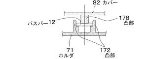
図6は、本発明の第3の実施の形態に係る電流センサ300の分解斜視図である。図7は、同電流センサ300の組立手順及び完成状態を示す斜視図である。ここでは、ホルダ71とカバー82とからなるケース70によって各相の構成を保持する。なお、磁気シールド体65は、第1の実施の形態と異なり、1カ所の空隙69を有する一体のものを用いている。
FIG. 6 is an exploded perspective view of a current sensor 300 according to the third embodiment of the present invention. FIG. 7 is a perspective view showing an assembly procedure and a completed state of the current sensor 300. Here, the configuration of each phase is held by a case 70 including a
ホルダ71は、有底で上部が開口した例えば直方体形状であり、向かい合う長側面の上部には凹部72が3つずつ存在し、各相のバスバー12が前記凹部72同士を渡すように配置される。ホルダ71の底面には筒状(ここでは角筒状)の凸部73が3つ形成され、これがホルダ71の内部にて各相の磁気シールド体65を位置決め保持するためのシールド収容部75を成している。各筒状の凸部73は向かい合う2カ所だけ部分的に高さが低くなって凹部74を形成し、ホルダ71の長側面に形成された前記凹部72とともにバスバー12を図7のようにガイドするようになっている。
The
絶縁基板13は、本実施の形態では各相について共通の回路基板を1つを用いる。この絶縁基板13は、各相のホールIC14を配置するIC搭載部131と、各IC搭載部を連結する連結部132と、連結部132から各IC搭載部の側方に突出したガイド部133とを有する。
In this embodiment, the insulating
組立の際には、まず各シールド収容部75に磁気シールド体65を配置し(図7(A)→(B))、その後、磁気シールド体65を貫通するようにバスバー12を凹部72、74に合わせて配置する(図7(B)→(C))。ここで、バスバー12に切欠125を形成しておけば、切欠125と凹部72とを嵌合することで長手方向の位置決めを確実に行うことができる。あるいは、図8のように、向かい合う凹部72間の距離と同じ長さだけバスバー12の中間部を端部よりも幅広として、当該幅広部分を向かい合う凹部72間に嵌めてもよい。このように、バスバー12の幅を部分的に変えることでホルダ71と所定の嵌合構造をとることができる。
At the time of assembly, first, the
バスバー12の配置後、各相のホールIC14を搭載した絶縁基板13をバスバー上に配置する(図7(C)→(D))。このとき、絶縁基板13のガイド部133を隣接する凸部73の間、及びホルダ71の短側面と凸部73の間に通す。これにより絶縁基板13及びホールIC14がバスバー12に対して確実に位置決めされる。最後にホルダ71にカバー82を嵌合させて完成となる(図7(D)→(E))
After the
本実施の形態によれば、第1の実施の形態と同様の効果を奏するとともに、バスバー12とホールIC14と磁気シールド体65(及び空隙69)の相対的な位置関係をケース70によって安定的に保持することができるため、位置ずれによる特性の悪化等を防止して電流センサとしての信頼性を高めることができる。また、各相の構成を単一のケース70で保持するので、取り扱いが容易である。さらに、ケース70すなわちホルダ71及びカバー82の少なくとも外面又は内面を磁性面とすれば、磁気シールド体65による磁気遮蔽のみならず、ケース70によっても外部磁界に対する磁気遮蔽の効果が得られる。あるいは、図7(E)に仮想線で示すようにケース70の外側を高透磁率の磁性材からなる磁気シールド外装体85で覆った場合も、外部磁界に対する磁気遮蔽の効果がさらに高められる。
According to the present embodiment, the same effects as those of the first embodiment can be obtained, and the relative positional relationship among the
図9(A),(B)は、ホルダ71にてバスバー12を保持する構成の別の例を示す説明図である。この場合、バスバー12に位置決め用の半抜き部123を形成しておき、この半抜き部123の凸側をホルダ71底面に形成された凹部77と嵌合させる。さらにカバー82側に凸部78を設けておき、この凸部78を前記半抜き部123の凹側に嵌合させる。
FIGS. 9A and 9B are explanatory views showing another example of a configuration in which the
図10は、ホルダ71にてバスバー12を保持する構成のさらに別の例を示す説明図である。この場合、ホルダ71の底面に1対の凸部172を先端同士の間隔がバスバー12の幅と一致するように形成し、基部側を幅狭としてバスバー12の配置面としている。そしてカバー82側に設けた凸部178でバスバー12を押圧し、前記2つの凸部172間に配置したバスバー12の位置ずれを防止する。
FIG. 10 is an explanatory view showing still another example of a configuration in which the
(第4の実施の形態)
図11は、本発明の第4の実施の形態の説明図である。なお、本図において、磁気シールド体の図示は省略している。本実施の形態では、バスバー12とホールIC14との間隔を広げるために絶縁性のスペーサ192を挿入する。スペーサ192は、先端が係止爪194となっているコの字型形状であり、バスバー12の長手方向中間位置に形成された切欠127に嵌合する。そしてスペーサ192上に絶縁基板13及びホールIC14が固定配置される。本実施の形態によれば、バスバー12とホールIC14との間隔を広げてゲインの適正化を図ることができ、また、バスバー12と絶縁基板13及びホールIC14との絶縁を確実にすることができる。
(Fourth embodiment)
FIG. 11 is an explanatory diagram of the fourth embodiment of the present invention. In the drawing, the illustration of the magnetic shield body is omitted. In the present embodiment, an insulating
以上、実施の形態を例に本発明を説明したが、実施の形態の各構成要素には請求項に記載の範囲で種々の変形が可能であることは当業者に理解されるところである。以下、変形例について触れる。 The present invention has been described above by taking the embodiment as an example. However, it will be understood by those skilled in the art that various modifications can be made to each component of the embodiment within the scope of the claims. Hereinafter, modifications will be described.
実施の形態では磁気シールド体の形状を角筒状としたが、変形例では図12(A)〜(C)のように長円筒状、円筒状又は楕円筒状としてもよい。 In the embodiment, the shape of the magnetic shield body is a rectangular tube shape, but in a modified example, it may be a long cylindrical shape, a cylindrical shape, or an elliptical cylindrical shape as shown in FIGS.
実施の形態ではバスバーの形状を平板状としたが、変形例では断面が正方形、円形又は楕円形等のものを採用してもよい。円形又は楕円形の場合、図12(D)のように絶縁基板やホールICの配置部分を平坦面に加工しておくとよい。 In the embodiment, the shape of the bus bar is a flat plate, but in a modified example, the bus bar may have a square, circular, or elliptical cross section. In the case of a circle or an ellipse, it is preferable to process the insulating substrate and the Hall IC placement portion into a flat surface as shown in FIG.
実施の形態では三相交流電流を検出対象としたが、変形例では単相交流あるいは直流電流を検出対象としてもよい。 In the embodiment, a three-phase alternating current is a detection target, but in a modified example, a single-phase alternating current or a direct current may be the detection target.
実施の形態ではホールIC14の近傍に磁気ヨークを設けない場合を説明したが、従来のリング状の磁気コア(図13参照)のように小型化を大きく阻害するものでなければ、磁気ヨークを設けてゲインを増大させてもよい。例えば、バスバー12の幅内に収まるようにホールIC14の片側又は両側に直線状の磁気ヨークを配置することは差し支えない。さらに、その直線状の磁気ヨークに巻線を施して図16のような回路を構成し、磁気平衡式の電流センサとしてもよい。
In the embodiment, the case where the magnetic yoke is not provided in the vicinity of the
12 バスバー
13 絶縁基板
14 ホールIC
62 上側磁気シールド部材
63 下側磁気シールド部材
65 磁気シールド体
67,68 空隙
100 電流センサ
12
62 Upper
Claims (10)
前記バスバーに流れる電流によって発生する磁界が感磁面に印加されるように前記バスバーに対して固定配置された磁気検出素子と、
前記磁気検出素子を磁気遮蔽する磁気シールド体とを備え、
前記磁気シールド体は、前記バスバーと前記磁気検出素子とを内側に囲む環状囲み部を有し、
前記環状囲み部には少なくとも1カ所の空隙が形成され、前記空隙が前記バスバーの側面と対向する位置にある又は前記バスバーの厚み寸法内に位置し、
前記バスバーが複数平行に設けられ、各バスバーに前記磁気検出素子が固定配置され、各バスバー及び各磁気検出素子に対して前記磁気シールド体が設けられ、
各バスバーの長手方向の中間部が所定の嵌合構造で単一のホルダに位置決め保持されている、電流センサ。 A bus bar,
A magnetic detection element fixedly arranged with respect to the bus bar so that a magnetic field generated by a current flowing through the bus bar is applied to a magnetic sensitive surface;
A magnetic shield body for magnetically shielding the magnetic detection element,
The magnetic shield body has an annular enclosure that encloses the bus bar and the magnetic detection element inside,
The gap of the at least one location in the annular surrounding member is formed, before Kisora gap is located within the thickness of a or the bus bar at a position facing the side surface of the bus bar,
A plurality of the bus bars are provided in parallel, the magnetic detection element is fixedly disposed on each bus bar, and the magnetic shield body is provided for each bus bar and each magnetic detection element,
A current sensor in which a middle portion in the longitudinal direction of each bus bar is positioned and held by a single holder with a predetermined fitting structure.
前記バスバーに流れる電流によって発生する磁界が感磁面に印加されるように前記バスバーに対して固定配置された磁気検出素子と、
前記磁気検出素子を磁気遮蔽する磁気シールド体とを備え、
前記磁気シールド体は、前記バスバーと前記磁気検出素子とを内側に囲む環状囲み部を有し、
前記環状囲み部には少なくとも1カ所の空隙が形成され、前記空隙が前記バスバーの側面と対向する位置にある又は前記バスバーの厚み寸法内に位置し、
前記バスバーが複数平行に設けられ、各バスバーに前記磁気検出素子が固定配置され、各バスバー及び各磁気検出素子に対して前記磁気シールド体が設けられ、
各磁気シールド体は、複数のシールド収容部を有する単一のホルダの各シールド収容部に位置決め保持されている、電流センサ。 A bus bar,
A magnetic detection element fixedly arranged with respect to the bus bar so that a magnetic field generated by a current flowing through the bus bar is applied to a magnetic sensitive surface;
A magnetic shield body for magnetically shielding the magnetic detection element,
The magnetic shield body has an annular enclosure that encloses the bus bar and the magnetic detection element inside,
The gap of the at least one location in the annular surrounding member is formed, before Kisora gap is located within the thickness of a or the bus bar at a position facing the side surface of the bus bar,
A plurality of the bus bars are provided in parallel, the magnetic detection element is fixedly disposed on each bus bar, and the magnetic shield body is provided for each bus bar and each magnetic detection element,
Each magnetic shield body is a current sensor which is positioned and held in each shield housing portion of a single holder having a plurality of shield housing portions.
Priority Applications (1)
| Application Number | Priority Date | Filing Date | Title |
|---|---|---|---|
| JP2008160855A JP5263494B2 (en) | 2008-06-19 | 2008-06-19 | Current sensor |
Applications Claiming Priority (1)
| Application Number | Priority Date | Filing Date | Title |
|---|---|---|---|
| JP2008160855A JP5263494B2 (en) | 2008-06-19 | 2008-06-19 | Current sensor |
Publications (2)
| Publication Number | Publication Date |
|---|---|
| JP2010002277A JP2010002277A (en) | 2010-01-07 |
| JP5263494B2 true JP5263494B2 (en) | 2013-08-14 |
Family
ID=41584128
Family Applications (1)
| Application Number | Title | Priority Date | Filing Date |
|---|---|---|---|
| JP2008160855A Active JP5263494B2 (en) | 2008-06-19 | 2008-06-19 | Current sensor |
Country Status (1)
| Country | Link |
|---|---|
| JP (1) | JP5263494B2 (en) |
Families Citing this family (33)
| Publication number | Priority date | Publication date | Assignee | Title |
|---|---|---|---|---|
| JP5482736B2 (en) | 2011-06-28 | 2014-05-07 | 株式会社デンソー | Current sensor |
| JP5960403B2 (en) * | 2011-09-26 | 2016-08-02 | 矢崎総業株式会社 | Current sensor |
| JP2013238580A (en) * | 2011-12-28 | 2013-11-28 | Tdk Corp | Current sensor |
| JP2013145165A (en) * | 2012-01-13 | 2013-07-25 | Denso Corp | Current sensor mechanism |
| JP5806134B2 (en) * | 2012-01-23 | 2015-11-10 | トヨタ自動車株式会社 | Power converter |
| JP2013246005A (en) * | 2012-05-24 | 2013-12-09 | Fujikura Ltd | Current sensor |
| JP5985257B2 (en) * | 2012-05-31 | 2016-09-06 | 矢崎総業株式会社 | Current sensor |
| JP5952650B2 (en) * | 2012-06-14 | 2016-07-13 | 矢崎総業株式会社 | Current sensor |
| JP6030866B2 (en) * | 2012-06-14 | 2016-11-24 | 矢崎総業株式会社 | Current sensor |
| JP6372969B2 (en) | 2012-12-03 | 2018-08-15 | 矢崎総業株式会社 | Current sensor |
| JP2014185999A (en) * | 2013-03-25 | 2014-10-02 | Omron Corp | Current sensor and power sensor using the same |
| JP6350785B2 (en) * | 2013-09-03 | 2018-07-04 | Tdk株式会社 | Inverter device |
| JP2015194472A (en) | 2014-01-23 | 2015-11-05 | 株式会社デンソー | current detection system |
| CN107076784B (en) | 2014-12-15 | 2019-06-14 | 株式会社村田制作所 | Current sensor |
| JP6149885B2 (en) * | 2015-03-18 | 2017-06-21 | トヨタ自動車株式会社 | Current sensor |
| WO2016203781A1 (en) * | 2015-06-15 | 2016-12-22 | 株式会社村田製作所 | Current sensor |
| WO2017217267A1 (en) * | 2016-06-15 | 2017-12-21 | 株式会社デンソー | Electric current sensor |
| JP6536553B2 (en) * | 2016-12-12 | 2019-07-03 | 株式会社デンソー | Current sensor |
| CN109313223B (en) * | 2016-06-15 | 2021-02-26 | 株式会社电装 | Current sensor |
| JP6536544B2 (en) * | 2016-06-15 | 2019-07-03 | 株式会社デンソー | Current sensor |
| WO2018003434A1 (en) * | 2016-06-30 | 2018-01-04 | 日立オートモティブシステムズ株式会社 | Current detection device |
| KR101871214B1 (en) * | 2016-08-19 | 2018-06-27 | 부산대학교 산학협력단 | Shield structure and current sensors |
| JP6699532B2 (en) * | 2016-12-12 | 2020-05-27 | 株式会社デンソー | Current sensor |
| JP6490130B2 (en) * | 2017-03-24 | 2019-03-27 | Tdk株式会社 | Magnetic sensor |
| JP2018169305A (en) * | 2017-03-30 | 2018-11-01 | 日立金属株式会社 | Current sensor |
| JP7003620B2 (en) * | 2017-12-14 | 2022-01-20 | 日立金属株式会社 | Current sensor |
| JP7322442B2 (en) * | 2019-03-15 | 2023-08-08 | Tdk株式会社 | current sensor |
| JP7259586B2 (en) | 2019-06-20 | 2023-04-18 | 株式会社デンソー | sensor unit |
| WO2022014266A1 (en) * | 2020-07-14 | 2022-01-20 | アルプスアルパイン株式会社 | Current detection device |
| JP2022091549A (en) * | 2020-12-09 | 2022-06-21 | 株式会社デンソー | Current sensor |
| CN113571975B (en) * | 2021-07-22 | 2024-05-14 | 阳光电源股份有限公司 | Copper bar assembly and electronic equipment |
| DE112022004664T5 (en) * | 2021-09-29 | 2024-07-18 | Murata Manufacturing Co., Ltd. | Current sensor, method for correcting the same and method for correcting a plurality of current sensors |
| JP2023073975A (en) * | 2021-11-16 | 2023-05-26 | 株式会社デンソー | current sensor |
Family Cites Families (6)
| Publication number | Priority date | Publication date | Assignee | Title |
|---|---|---|---|---|
| JPS5982867U (en) * | 1982-11-25 | 1984-06-04 | 三菱電機株式会社 | current measuring device |
| JP2890650B2 (en) * | 1990-04-14 | 1999-05-17 | 株式会社豊田自動織機製作所 | Current sensor |
| JPH0792199A (en) * | 1993-07-28 | 1995-04-07 | Matsushita Electric Ind Co Ltd | Current sensor |
| JP2001289884A (en) * | 2000-04-04 | 2001-10-19 | Mitsubishi Electric Corp | Current sensor |
| JP2006112968A (en) * | 2004-10-15 | 2006-04-27 | Toyota Motor Corp | Current detecting device |
| JP4629644B2 (en) * | 2006-10-31 | 2011-02-09 | 株式会社東海理化電機製作所 | Current detector |
-
2008
- 2008-06-19 JP JP2008160855A patent/JP5263494B2/en active Active
Also Published As
| Publication number | Publication date |
|---|---|
| JP2010002277A (en) | 2010-01-07 |
Similar Documents
| Publication | Publication Date | Title |
|---|---|---|
| JP5263494B2 (en) | Current sensor | |
| JP2010008050A (en) | Current sensor | |
| JP4835868B2 (en) | Current sensor | |
| JP5680287B2 (en) | Current sensor | |
| JP6350785B2 (en) | Inverter device | |
| US20130169267A1 (en) | Current sensor | |
| US9069016B2 (en) | Current sensor | |
| JP4788922B2 (en) | Current sensor | |
| JP5098855B2 (en) | Current sensor | |
| JP2010071822A (en) | Current sensor | |
| CN108450013B (en) | Current sensor and power conversion device provided with same | |
| JP2007121283A (en) | Assembly group for current measurement | |
| JP2008215970A (en) | Bus bar integrated current sensor | |
| JP5252207B2 (en) | Reactor and converter | |
| JP2014160035A (en) | Current sensor | |
| JP2018189504A (en) | Curent sensor | |
| JP2013120177A (en) | Current detector | |
| JP5067574B2 (en) | Current sensor | |
| JP2014006116A (en) | Inverter | |
| JP6384677B2 (en) | Current sensor | |
| JP2014020980A (en) | Current sensor, bus bar device with sensor equipped with the same, inverter device, and connector | |
| JP2006038518A (en) | Current measuring instrument | |
| JP2015132534A (en) | Current detection device | |
| JP2008128915A (en) | Amperometric device and semiconductor module equipped with amperometric function | |
| JP2011158337A (en) | Current sensor |
Legal Events
| Date | Code | Title | Description |
|---|---|---|---|
| A621 | Written request for application examination |
Free format text: JAPANESE INTERMEDIATE CODE: A621 Effective date: 20110125 |
|
| A977 | Report on retrieval |
Free format text: JAPANESE INTERMEDIATE CODE: A971007 Effective date: 20120510 |
|
| A131 | Notification of reasons for refusal |
Free format text: JAPANESE INTERMEDIATE CODE: A131 Effective date: 20120516 |
|
| A521 | Written amendment |
Free format text: JAPANESE INTERMEDIATE CODE: A523 Effective date: 20120712 |
|
| A131 | Notification of reasons for refusal |
Free format text: JAPANESE INTERMEDIATE CODE: A131 Effective date: 20120829 |
|
| A521 | Written amendment |
Free format text: JAPANESE INTERMEDIATE CODE: A523 Effective date: 20121017 |
|
| A131 | Notification of reasons for refusal |
Free format text: JAPANESE INTERMEDIATE CODE: A131 Effective date: 20130109 |
|
| A521 | Written amendment |
Free format text: JAPANESE INTERMEDIATE CODE: A523 Effective date: 20130305 |
|
| TRDD | Decision of grant or rejection written | ||
| A01 | Written decision to grant a patent or to grant a registration (utility model) |
Free format text: JAPANESE INTERMEDIATE CODE: A01 Effective date: 20130403 |
|
| A61 | First payment of annual fees (during grant procedure) |
Free format text: JAPANESE INTERMEDIATE CODE: A61 Effective date: 20130416 |
|
| R150 | Certificate of patent or registration of utility model |
Free format text: JAPANESE INTERMEDIATE CODE: R150 Ref document number: 5263494 Country of ref document: JP Free format text: JAPANESE INTERMEDIATE CODE: R150 |