JP7003620B2 - Current sensor - Google Patents
Current sensor Download PDFInfo
- Publication number
- JP7003620B2 JP7003620B2 JP2017240048A JP2017240048A JP7003620B2 JP 7003620 B2 JP7003620 B2 JP 7003620B2 JP 2017240048 A JP2017240048 A JP 2017240048A JP 2017240048 A JP2017240048 A JP 2017240048A JP 7003620 B2 JP7003620 B2 JP 7003620B2
- Authority
- JP
- Japan
- Prior art keywords
- bus bar
- plate thickness
- thickness direction
- circuit board
- housings
- Prior art date
- Legal status (The legal status is an assumption and is not a legal conclusion. Google has not performed a legal analysis and makes no representation as to the accuracy of the status listed.)
- Active
Links
Images


Classifications
-
- G—PHYSICS
- G01—MEASURING; TESTING
- G01R—MEASURING ELECTRIC VARIABLES; MEASURING MAGNETIC VARIABLES
- G01R19/00—Arrangements for measuring currents or voltages or for indicating presence or sign thereof
- G01R19/0092—Arrangements for measuring currents or voltages or for indicating presence or sign thereof measuring current only
-
- G—PHYSICS
- G01—MEASURING; TESTING
- G01R—MEASURING ELECTRIC VARIABLES; MEASURING MAGNETIC VARIABLES
- G01R15/00—Details of measuring arrangements of the types provided for in groups G01R17/00 - G01R29/00, G01R33/00 - G01R33/26 or G01R35/00
- G01R15/14—Adaptations providing voltage or current isolation, e.g. for high-voltage or high-current networks
- G01R15/20—Adaptations providing voltage or current isolation, e.g. for high-voltage or high-current networks using galvano-magnetic devices, e.g. Hall-effect devices, i.e. measuring a magnetic field via the interaction between a current and a magnetic field, e.g. magneto resistive or Hall effect devices
- G01R15/207—Constructional details independent of the type of device used
-
- G—PHYSICS
- G01—MEASURING; TESTING
- G01R—MEASURING ELECTRIC VARIABLES; MEASURING MAGNETIC VARIABLES
- G01R1/00—Details of instruments or arrangements of the types included in groups G01R5/00 - G01R13/00 and G01R31/00
- G01R1/02—General constructional details
- G01R1/04—Housings; Supporting members; Arrangements of terminals
-
- G—PHYSICS
- G01—MEASURING; TESTING
- G01R—MEASURING ELECTRIC VARIABLES; MEASURING MAGNETIC VARIABLES
- G01R15/00—Details of measuring arrangements of the types provided for in groups G01R17/00 - G01R29/00, G01R33/00 - G01R33/26 or G01R35/00
- G01R15/14—Adaptations providing voltage or current isolation, e.g. for high-voltage or high-current networks
- G01R15/146—Measuring arrangements for current not covered by other subgroups of G01R15/14, e.g. using current dividers, shunts, or measuring a voltage drop
- G01R15/148—Measuring arrangements for current not covered by other subgroups of G01R15/14, e.g. using current dividers, shunts, or measuring a voltage drop involving the measuring of a magnetic field or electric field
-
- G—PHYSICS
- G01—MEASURING; TESTING
- G01R—MEASURING ELECTRIC VARIABLES; MEASURING MAGNETIC VARIABLES
- G01R15/00—Details of measuring arrangements of the types provided for in groups G01R17/00 - G01R29/00, G01R33/00 - G01R33/26 or G01R35/00
- G01R15/14—Adaptations providing voltage or current isolation, e.g. for high-voltage or high-current networks
- G01R15/20—Adaptations providing voltage or current isolation, e.g. for high-voltage or high-current networks using galvano-magnetic devices, e.g. Hall-effect devices, i.e. measuring a magnetic field via the interaction between a current and a magnetic field, e.g. magneto resistive or Hall effect devices
- G01R15/202—Adaptations providing voltage or current isolation, e.g. for high-voltage or high-current networks using galvano-magnetic devices, e.g. Hall-effect devices, i.e. measuring a magnetic field via the interaction between a current and a magnetic field, e.g. magneto resistive or Hall effect devices using Hall-effect devices
-
- G—PHYSICS
- G01—MEASURING; TESTING
- G01R—MEASURING ELECTRIC VARIABLES; MEASURING MAGNETIC VARIABLES
- G01R15/00—Details of measuring arrangements of the types provided for in groups G01R17/00 - G01R29/00, G01R33/00 - G01R33/26 or G01R35/00
- G01R15/14—Adaptations providing voltage or current isolation, e.g. for high-voltage or high-current networks
- G01R15/20—Adaptations providing voltage or current isolation, e.g. for high-voltage or high-current networks using galvano-magnetic devices, e.g. Hall-effect devices, i.e. measuring a magnetic field via the interaction between a current and a magnetic field, e.g. magneto resistive or Hall effect devices
- G01R15/205—Adaptations providing voltage or current isolation, e.g. for high-voltage or high-current networks using galvano-magnetic devices, e.g. Hall-effect devices, i.e. measuring a magnetic field via the interaction between a current and a magnetic field, e.g. magneto resistive or Hall effect devices using magneto-resistance devices, e.g. field plates
-
- G—PHYSICS
- G01—MEASURING; TESTING
- G01R—MEASURING ELECTRIC VARIABLES; MEASURING MAGNETIC VARIABLES
- G01R31/00—Arrangements for testing electric properties; Arrangements for locating electric faults; Arrangements for electrical testing characterised by what is being tested not provided for elsewhere
- G01R31/28—Testing of electronic circuits, e.g. by signal tracer
- G01R31/302—Contactless testing
- G01R31/315—Contactless testing by inductive methods
-
- G—PHYSICS
- G01—MEASURING; TESTING
- G01R—MEASURING ELECTRIC VARIABLES; MEASURING MAGNETIC VARIABLES
- G01R33/00—Arrangements or instruments for measuring magnetic variables
- G01R33/02—Measuring direction or magnitude of magnetic fields or magnetic flux
-
- H—ELECTRICITY
- H01—ELECTRIC ELEMENTS
- H01R—ELECTRICALLY-CONDUCTIVE CONNECTIONS; STRUCTURAL ASSOCIATIONS OF A PLURALITY OF MUTUALLY-INSULATED ELECTRICAL CONNECTING ELEMENTS; COUPLING DEVICES; CURRENT COLLECTORS
- H01R25/00—Coupling parts adapted for simultaneous co-operation with two or more identical counterparts, e.g. for distributing energy to two or more circuits
- H01R25/16—Rails or bus-bars provided with a plurality of discrete connecting locations for counterparts
-
- G—PHYSICS
- G01—MEASURING; TESTING
- G01N—INVESTIGATING OR ANALYSING MATERIALS BY DETERMINING THEIR CHEMICAL OR PHYSICAL PROPERTIES
- G01N17/00—Investigating resistance of materials to the weather, to corrosion, or to light
- G01N17/02—Electrochemical measuring systems for weathering, corrosion or corrosion-protection measurement
-
- G—PHYSICS
- G01—MEASURING; TESTING
- G01N—INVESTIGATING OR ANALYSING MATERIALS BY DETERMINING THEIR CHEMICAL OR PHYSICAL PROPERTIES
- G01N27/00—Investigating or analysing materials by the use of electric, electrochemical, or magnetic means
- G01N27/72—Investigating or analysing materials by the use of electric, electrochemical, or magnetic means by investigating magnetic variables
- G01N27/82—Investigating or analysing materials by the use of electric, electrochemical, or magnetic means by investigating magnetic variables for investigating the presence of flaws
- G01N27/83—Investigating or analysing materials by the use of electric, electrochemical, or magnetic means by investigating magnetic variables for investigating the presence of flaws by investigating stray magnetic fields
-
- G—PHYSICS
- G01—MEASURING; TESTING
- G01N—INVESTIGATING OR ANALYSING MATERIALS BY DETERMINING THEIR CHEMICAL OR PHYSICAL PROPERTIES
- G01N27/00—Investigating or analysing materials by the use of electric, electrochemical, or magnetic means
- G01N27/72—Investigating or analysing materials by the use of electric, electrochemical, or magnetic means by investigating magnetic variables
- G01N27/82—Investigating or analysing materials by the use of electric, electrochemical, or magnetic means by investigating magnetic variables for investigating the presence of flaws
- G01N27/90—Investigating or analysing materials by the use of electric, electrochemical, or magnetic means by investigating magnetic variables for investigating the presence of flaws using eddy currents
- G01N27/9046—Investigating or analysing materials by the use of electric, electrochemical, or magnetic means by investigating magnetic variables for investigating the presence of flaws using eddy currents by analysing electrical signals
Landscapes
- Physics & Mathematics (AREA)
- General Physics & Mathematics (AREA)
- Condensed Matter Physics & Semiconductors (AREA)
- Engineering & Computer Science (AREA)
- General Engineering & Computer Science (AREA)
- Measuring Instrument Details And Bridges, And Automatic Balancing Devices (AREA)
Description
本発明は、電流センサに関する。 The present invention relates to a current sensor.
従来、電流センサとして、測定対象となる電流により発生する磁界の強度を検出する磁気検出素子を備えたものが知られている。磁気検出素子により磁界の強度を検出することで、その磁界の強度を基に、電流を演算により求めることが可能である。この種の電流センサとして、電流路となるバスバと磁気検出素子とをハウジングで覆ったものが知られている(例えば、特許文献1参照)。 Conventionally, as a current sensor, a sensor including a magnetic detection element for detecting the strength of a magnetic field generated by a current to be measured is known. By detecting the strength of the magnetic field with the magnetic detection element, it is possible to obtain the current by calculation based on the strength of the magnetic field. As a current sensor of this type, a sensor in which a bus bar serving as a current path and a magnetic detection element are covered with a housing is known (see, for example, Patent Document 1).
電流センサでは、バスバに対する磁気検出素子の位置ずれをなるべく小さくすることが望まれる。バスバと板厚方向に対向して磁気検出素子を配置する場合、板厚方向に沿ったバスバと磁気検出間の距離は一定に保たれる必要がある。そこで、バスバと回路基板とを直接、あるいはスペーサ等を介して間接的に当接させ、バスバと回路基板とを挟み込む上下のハウジングによって、バスバの板厚方向に所定の押圧力を加えることで(押圧力を加えた状態で上下のハウジングを互いに固定することで)、バスバと磁気検出素子間の距離を一定に保つことが考えられる。 In the current sensor, it is desired to minimize the displacement of the magnetic detection element with respect to the bus bar. When the magnetic detection element is arranged so as to face the bus bar in the plate thickness direction, the distance between the bus bar and the magnetic detection along the plate thickness direction needs to be kept constant. Therefore, the bus bar and the circuit board are brought into contact with each other directly or indirectly via a spacer or the like, and a predetermined pressing force is applied in the plate thickness direction of the bus bar by the upper and lower housings that sandwich the bus bar and the circuit board ( It is conceivable to keep the distance between the bus bar and the magnetic detection element constant by fixing the upper and lower housings to each other while applying a pressing force).
しかしながら、上記の電流センサでは、上下のハウジングが板厚方向に互いに当接していると、製造公差等によりハウジング内で隙間が生じ、バスバと回路基板間に十分な押圧力を加えられない場合があった。これは、バスバ、回路基板、スペーサ、上下のハウジング等の複数の部材を積層するために、各部材の公差の影響が積み重なり、ハウジング内で隙間が生じるおそれが大きくなるためである。 However, in the above current sensor, if the upper and lower housings are in contact with each other in the plate thickness direction, a gap may be created in the housing due to manufacturing tolerances, etc., and sufficient pressing force may not be applied between the bus bar and the circuit board. there were. This is because a plurality of members such as a bus bar, a circuit board, a spacer, and upper and lower housings are laminated, so that the influence of the tolerance of each member is accumulated and the possibility of a gap in the housing increases.
本発明者らは、上下のハウジングが互いに当接しないようにすること(積層時に上下のハウジング間に隙間が生じるように構成すること)を検討した。これにより、各部材の公差の影響を吸収して、バスバと回路基板間に押圧力を付与することが可能になる。しかしこの場合、上下のハウジングをボルト固定等で固定した際に、隙間の部分でハウジングが凹むなどしてハウジングが変形してしまう場合があった。ハウジングが変形すると押圧力が偏り、押圧力が弱い部分で浮きが発生する等して部材が傾いてしまうため、バスバと磁気検出素子の位置ずれが生じてしまうおそれが生じる。 The present inventors have studied so that the upper and lower housings do not come into contact with each other (the structure is such that a gap is formed between the upper and lower housings during stacking). This makes it possible to absorb the influence of the tolerance of each member and apply a pressing force between the bus bar and the circuit board. However, in this case, when the upper and lower housings are fixed by bolting or the like, the housing may be deformed due to a dent in the gap portion. When the housing is deformed, the pressing force is biased, and the member is tilted due to floating at a portion where the pressing force is weak, so that there is a possibility that the position of the bus bar and the magnetic detection element may be displaced.
そこで、本発明は、バスバと磁気検出素子の位置ずれを抑制可能な電流センサを提供することを目的とする。 Therefore, an object of the present invention is to provide a current sensor capable of suppressing the positional deviation between the bus bar and the magnetic detection element.
本発明は、上記課題を解決することを目的として、検出対象の電流が流れる帯状かつ板状のバスバと、前記バスバの表裏面に垂直な板厚方向において前記バスバと対向して配置され、前記バスバを流れる電流により発生する磁界の強度を検出する磁気検出素子が搭載された回路基板と、前記バスバの板厚方向において、前記バスバと前記回路基板とを挟み込むように前記板厚方向に対向して設けられ、前記バスバと前記回路基板とを板厚方向に押さえつけた状態で互いに固定される第1及び第2ハウジングを有するハウジングと、を備え、前記第1及び第2ハウジングは、前記板厚方向において前記バスバ及び前記回路基板と重ならない位置であって前記板厚方向に対向する位置に、法線方向が前記バスバの板厚方向に対して傾斜した方向となる傾斜面をそれぞれ有し、前記傾斜面同士を互いに当接しつつ、前記傾斜面に沿った方向に滑らせて前記第1及び第2ハウジングを相対的にスライドさせることで、前記第1及び第2ハウジングにより前記バスバと前記回路基板とを板厚方向に押さえつけることが可能なスライドガイド部を有しており、前記第1及び第2ハウジングは、少なくとも、前記スライドガイド部において、ボルトとナットとを用いて前記第1及び第2ハウジングを板厚方向に締め付けた状態で固定するボルト固定、あるいは、前記第2ハウジングの前記傾斜面から前記板厚方向に突出する熱かしめ用突起を、前記第1ハウジングの前記傾斜面に形成された孔に挿入し前記熱かしめ用突起の先端を加熱溶融させることで、前記第1及び第2ハウジングを板厚方向に締め付けた状態で固定する熱かしめにより互いに固定されている、電流センサを提供する。 The present invention has a strip-shaped and plate-shaped bus bar through which a current to be detected flows, and the bus bar is arranged to face the bus bar in the plate thickness direction perpendicular to the front and back surfaces of the bus bar, for the purpose of solving the above problems. A circuit board on which a magnetic detection element for detecting the strength of a magnetic field generated by a current flowing through a bus bar is mounted, and the bus bar face each other in the plate thickness direction so as to sandwich the bus bar and the circuit board. The first and second housings are provided with a housing having first and second housings which are fixed to each other while pressing the bus bar and the circuit board in the plate thickness direction, and the first and second housings are provided with the plate thickness. Each has an inclined surface whose normal direction is inclined with respect to the plate thickness direction of the bus bar at a position not overlapping the bus bar and the circuit board in the direction and facing the plate thickness direction. The first and second housings slide the first and second housings relative to each other by sliding the inclined surfaces in contact with each other in a direction along the inclined surfaces, whereby the bus bar and the circuit are provided by the first and second housings. The first and second housings have a slide guide portion capable of pressing the substrate in the plate thickness direction, and the first and second housings have at least the first and second housings using bolts and nuts in the slide guide portion. 2 Bolt fixing for fixing the housing in a state of being tightened in the plate thickness direction, or forming a heat caulking protrusion protruding from the inclined surface of the second housing in the plate thickness direction on the inclined surface of the first housing. A current sensor that is fixed to each other by heat caulking that fixes the first and second housings in a state of being tightened in the plate thickness direction by inserting them into the holes and heating and melting the tips of the heat caulking protrusions. offer.
本発明によれば、バスバと磁気検出素子の位置ずれを抑制可能な電流センサを提供できる。 According to the present invention, it is possible to provide a current sensor capable of suppressing a misalignment between a bus bar and a magnetic detection element.
[実施の形態]
以下、本発明の実施の形態を添付図面にしたがって説明する。
[Embodiment]
Hereinafter, embodiments of the present invention will be described with reference to the accompanying drawings.
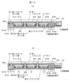
図1(a),(b)は、本発明の一実施の形態に係る電流センサを示す斜視図である。図2,3は、電流センサの分解斜視図である。 1 (a) and 1 (b) are perspective views showing a current sensor according to an embodiment of the present invention. 2 and 3 are exploded perspective views of the current sensor.
図1~3に示すように、電流センサ1は、検出対象の電流が流れるバスバ2と、磁気検出素子3と、磁気検出素子3が搭載された回路基板4と、スペーサ5と、第1ハウジング61及び第2ハウジング62を有する2分割構造のハウジング6と、を有している。なお、図1~3では、後述するシールド板7を省略して示している(図7参照)。 As shown in FIGS. 1 to 3, the current sensor 1 includes a bus bar 2 through which a current to be detected flows, a magnetic detection element 3, a circuit board 4 on which the magnetic detection element 3 is mounted, a spacer 5, and a first housing. It has a housing 6 having a two-part structure having a 61 and a second housing 62. In FIGS. 1 to 3, the shield plate 7 described later is omitted (see FIG. 7).
(バスバ2の説明)
バスバ2は、銅やアルミニウム等の電気良導体からなる板状の導体であり、電流を流す電流路となるものである。バスバ2は、例えば電気自動車やハイブリッド車におけるモータとインバータ間の電源ラインとして用いられるものである。本実施の形態では、三相交流に対応した3本のバスバ2を用いる場合を説明する。ただし、バスバ2の本数はこれに限定されない。バスバ2の厚さは、例えば3mmである。3本のバスバ2a~2cは、その板幅方向に離間して整列配置されている。
(Explanation of Busba 2)
The bus bar 2 is a plate-shaped conductor made of a good electric conductor such as copper or aluminum, and serves as a current path through which a current flows. The bus bar 2 is used as a power supply line between a motor and an inverter in, for example, an electric vehicle or a hybrid vehicle. In this embodiment, a case where three bus bars 2 corresponding to three-phase alternating current are used will be described. However, the number of bus bars 2 is not limited to this. The thickness of the bus bar 2 is, for example, 3 mm. The three
各バスバ2a~2cには、それぞれ2つの切欠き21が形成されている。2つの切欠き21は、各バスバ2a~2cの板幅方向における両側方へとそれぞれ開口するように形成されると共に、長さ方向における略同じ位置で板幅方向に対向するように形成されている。各バスバ2a~2cに2つの切欠き21を形成することにより、バスバ2a~2cの長手方向の一部が幅狭となった狭幅部22が形成されている。本実施の形態では、この狭幅部22と厚さ方向に対向するように、磁気検出素子3が配置される。
Two
狭幅部22は、高周波における表皮効果の影響を抑制する役割を果たし、検出精度の向上に寄与する。より詳細には、バスバ2に高周波の電流が流れると、表皮効果により電流分布がバスバ2の表面に偏る。周波数によって表皮厚さが異なり、バスバ2内部の電流分布が変わるため、磁気検出素子3の位置における磁束密度が変化してしまう。バスバ2の幅方向における中央部と対向するように磁気検出素子3を配置する場合、磁気検出素子3側から見て、バスバ2の通電面の断面形状のアスペクト比が小さい方が電流分布の広がり(すなわち電流分布の周波数依存性)が小さくなり、表皮効果の影響が小さくなると考えられる。
The
(磁気検出素子3及び回路基板4の説明)
磁気検出素子3は、対応するバスバ2a~2cを流れる電流により発生する磁界の強度を検出するものである。ここでは、1本のバスバ2に対して2つの磁気検出素子3を用いる場合を示しており、合計6つの磁気検出素子3を用いる場合示している。ただし、これに限らず、1本のバスバ2に対して1つの磁気検出素子3を用いるように構成してもよい。磁気検出素子3としては、例えば、ホール素子やGMR(Giant Magneto Resistive effect)素子、AMR(Anisotropic Magneto Resistive)素子、TMR(Tunneling Magneto Resistive)素子等を用いることができる。
(Explanation of Magnetic Detection Element 3 and Circuit Board 4)
The magnetic detection element 3 detects the strength of the magnetic field generated by the current flowing through the
磁気検出素子3は、検出軸に沿った方向の磁界の強度(磁束密度)に応じた電圧の出力信号を出力するように構成されている。本実施の形態では、各磁気検出素子3は、検出軸がバスバ2の板幅方向と一致するように配置されている。 The magnetic detection element 3 is configured to output an output signal having a voltage corresponding to the strength (magnetic flux density) of the magnetic field in the direction along the detection axis. In the present embodiment, each magnetic detection element 3 is arranged so that the detection axis coincides with the plate width direction of the bus bar 2.
各磁気検出素子3は、共通の回路基板4に搭載されている。回路基板4には、第1ハウジング61に対する位置決めを行うための2つの位置決め用孔41が形成されている。また、回路基板4には、第2ハウジング62の熱かしめ用突起62aを通すための長孔42が形成されている。詳細は後述するが、本実施の形態では、組立時に、第1ハウジング61(及び第1ハウジング61に固定された回路基板4)に対して、バスバ2の板幅方向と垂直な方向に第2ハウジング62がスライドする。そのため、回路基板4に対して熱かしめ用突起62aがスライド移動できるように、長孔42は、バスバ2の長さ方向に延びる長円形状(角丸長方形状)に形成されている。位置決め用孔41及び長孔42は、共に回路基板4を板厚方向に貫通するように形成されている。回路基板4の端部には、電源供給や磁気検出素子3の検出信号の出力等に用いられるコネクタ43が設けられている。
Each magnetic detection element 3 is mounted on a common circuit board 4. The circuit board 4 is formed with two
(スペーサ5の説明)
図4は、スペーサ5と回路基板4の斜視図である。スペーサ5は、バスバ2と回路基板4との間に設けられ、バスバ2と回路基板4(磁気検出素子3)とを所定の間隔に維持するためのものである。スペーサ5は、例えばPPS(ポリフェニレンサルファイド)、PBT(ポリブチレンテレフタレート)等の樹脂からなり、板状に形成されている。
(Explanation of spacer 5)
FIG. 4 is a perspective view of the spacer 5 and the circuit board 4. The spacer 5 is provided between the bus bar 2 and the circuit board 4, and is for maintaining the bus bar 2 and the circuit board 4 (magnetic detection element 3) at a predetermined interval. The spacer 5 is made of a resin such as PPS (polyphenylene sulfide) or PBT (polybutylene terephthalate), and is formed in a plate shape.
スペーサ5には、第1ハウジング61に対する位置決めを行うための2つの位置決め用孔51が形成されている。また、スペーサ5には、第2ハウジング62の熱かしめ用突起62aを通すための長孔52が形成されている。スペーサ5に対して熱かしめ用突起62aがスライド移動できるように、長孔52は、バスバ2の長さ方向に延びる長円形状(角丸長方形状)に形成されている。また、スペーサ5には、磁気検出素子3を収容するための3つの収容孔53が形成されている。各収容孔53には、2つずつの磁気検出素子3が収容されている。位置決め用孔51、長孔52、及び収容孔53は、共にスペーサ5を板厚方向に貫通するように形成されている。
The spacer 5 is formed with two
(ハウジング6の説明)
図5(a),(b)は、第1ハウジング61の斜視図である。図6は、第2ハウジング62の斜視図である。ハウジング6は、バスバ2の板厚方向において、バスバ2、回路基板4、及びスペーサ5を挟み込むように設けられた第1及び第2ハウジング61,62を有している。第1及び第2ハウジング61,62は、3本のバスバ2と回路基板4とを一括して挟み込むように設けられている。第1ハウジング61及び第2ハウジング62は、PPS(ポリフェニレンサルファイド),PBT(ポリブチレンテレフタレート)等の樹脂からなる。
(Explanation of housing 6)
5 (a) and 5 (b) are perspective views of the first housing 61. FIG. 6 is a perspective view of the second housing 62. The housing 6 has first and second housings 61 and 62 provided so as to sandwich the bus bar 2, the circuit board 4, and the spacer 5 in the plate thickness direction of the bus bar 2. The first and second housings 61 and 62 are provided so as to collectively sandwich the three bus bars 2 and the circuit board 4. The first housing 61 and the second housing 62 are made of a resin such as PPS (polyphenylene sulfide) and PBT (polybutylene terephthalate).
図5に示すように、第1ハウジング61は、バスバ2を収容するバスバ収容溝610aが形成された上蓋部610と、バスバ2の板幅方向における上蓋部610の一側に設けられた第1スライドガイド部611と、バスバ2の板幅方向における上蓋部610の他側に設けられた側壁部612と、を一体に有している。以下、説明を容易とするため、図5(a),(b)における上側を上、下側を下として説明する。なお、これら上下の方向は、電流センサ1の使用状態における上下を表すものではなく、電流センサ1の設置姿勢は適宜設定可能である。
As shown in FIG. 5, the first housing 61 is provided on one side of the
上蓋部610の下面(第2ハウジング62側の面)には、第1スライドガイド部611と側壁部612との対向方向に対して垂直方向に延びるように、3本のバスバ収容溝610aが等間隔に形成されている。各バスバ収容溝610aの間には、下方に突出する2つの突出部610bが形成されている。この突出部610bは、バスバ収容溝610a内に突出しバスバ2の切欠き21に嵌合する凸部610cを有している。凸部610cをバスバ2の切欠き21に嵌合させることで、バスバ2の第1ハウジング61に対する位置決めがなされる。
On the lower surface (the surface on the second housing 62 side) of the
また、2つの突出部610bには、下方に突出する位置決め突起610dがそれぞれ形成されている。両位置決め突起610dを、スペーサ5と回路基板4の位置決め用孔41,51に挿入することで、第1ハウジング61に対するスペーサ5及び回路基板4の位置決めがなされる。
Further, each of the two
上蓋部610の上面には、上方に突出するように一対のリブ状の突起610eが形成されている。両突起610eは、バスバ2の板幅方向に延びるように直線状に形成されており、上蓋部610の長さ方向(バスバ2の長さ方向)における端部の近傍に、長さ方向に対向するように形成されている。両突起610eには、両突起610eを長さ方向に貫通する係止孔610fが2つずつ形成されている。
A pair of rib-shaped
図7に示すように、第1ハウジング61には、シールド板7が固定される。シールド板7は、磁性材料からなり、外部からの磁界が磁気検出素子3の検出結果に影響を及ぼさないように、外部からの磁界を遮蔽するためのものである。シールド板7には、側方に突出する係止片7aが形成されており、この係止片7aを係止孔610fに係止させることで、ハウジング6の上部に固定される。
As shown in FIG. 7, a shield plate 7 is fixed to the first housing 61. The shield plate 7 is made of a magnetic material and is for shielding the magnetic field from the outside so that the magnetic field from the outside does not affect the detection result of the magnetic detection element 3. A
同様に、第1スライドガイド部611と側壁部612には、下方に突出するリブ状の突起611a,612aがそれぞれ形成されており、これら突起611a,612aに形成された係止孔611b,612b(図5(b)参照)に係止片7aを係止させることで、他のシールド板7がハウジング6の下部に固定される。つまり、電流センサ1は、バスバ2及び磁気検出素子3が、一対のシールド板7で挟み込まれた構造となっている。
Similarly, the first slide guide portion 611 and the
電流センサ1では、バスバ2や回路基板4を固定するハウジング6にシールド板7を取り付けることで、バスバ2及び磁気検出素子3に対するシールド板7の位置決めがなされ、各部材の相対的な位置関係が固定されることになる。本実施の形態においては、突起610e,611a,612a及び係止孔610f,611b,612bが、ハウジング6にシールド板7を保持するシールド板保持部としての役割を果たしている。
In the current sensor 1, by attaching the shield plate 7 to the housing 6 for fixing the bus bar 2 and the circuit board 4, the shield plate 7 is positioned with respect to the bus bar 2 and the magnetic detection element 3, and the relative positional relationship of each member is established. It will be fixed. In the present embodiment, the
図5に戻り、上蓋部610及び第1スライドガイド部611には、第2ハウジング62の熱かしめ用突起62aを通すための長孔61aが形成されている。本実施の形態では、組立時に、第1ハウジング61に対して、バスバ2の板幅方向と垂直な方向に第2ハウジング62がスライドする。そのため、熱かしめ用突起62aがスライド移動できるように、長孔61aは、バスバ2の長さ方向に延びる長円形状(角丸長方形状)に形成されている。本実施の形態では、上蓋部610に4つ、第1スライドガイド部611に2つの、合計6つの長孔61aを形成した。長孔61aは、上蓋部610及び第1スライドガイド部611を板厚方向に貫通するように形成されている。
Returning to FIG. 5, the
スライドガイド部611と側壁部612とは、3本のバスバ2、スペーサ5、及び回路基板4を、バスバ2の板幅方向において挟み込むように設けられている。側壁部612は、下方に開口する凹状の切欠き612cを有しており、この切欠き612cに、第2ハウジング62の下蓋部620(後述する)の端部が挿入されるようになっている。また、電流センサ1では、第1及び第2ハウジング61,62を互いに組み合わせた際には、側壁部612における切欠き612cの底面(上面)と第2ハウジング62(下蓋部620の端部)との間に隙間が形成されるようになっており、この隙間から、回路基板4の一部(コネクタ43を搭載する部分)が側方へと延出される。第1スライドガイド部611の詳細については後述する。
The slide guide portion 611 and the
図6に示すように、第2ハウジング62は、回路基板4の下面に当接する板状の下蓋部620と、バスバ2の板幅方向における下蓋部620の一側に設けられた第2スライドガイド部621と、を一体に有している。バスバ2の長さ方向における下蓋部620の両端部は他部に比較して厚く形成された縁部620aとなっている。第2スライドガイド部621は、下蓋部620から上方に突出するように設けられている。第2スライドガイド部621の詳細については後述する。下蓋部620と第2スライドガイド部621には、上方に突出する円柱状の熱かしめ用突起62aが形成されている。本実施の形態では、下蓋部620に4つ、第2スライドガイド部621に2つの、合計6つの熱かしめ用突起62aを形成した。
As shown in FIG. 6, the second housing 62 is provided on one side of a plate-shaped
(スライドガイド部611,621の説明)
スライドガイド部611,621は、バスバ2の板厚方向に互いに当接しつつ、バスバ2の板厚方向に対して傾斜した方向に、第1及び第2ハウジング61,62を相対的にスライド可能とするためのものである。本実施の形態では、スライドガイド部611,621は、第1及び第2ハウジング61,62を、バスバ2の板幅方向に垂直で、かつバスバ2の板厚方向及び長さ方向に対して傾斜した方向に相対的にスライド可能に形成されている。換言すれば、第1及び第2ハウジング61,62は、バスバ2の長さ方向にスライドしつつ、バスバ2の板厚方向にスライドする。
(Explanation of slide guides 611,621)
The slide guide portions 611 and 621 are capable of relatively sliding the first and second housings 61 and 62 in a direction inclined with respect to the plate thickness direction of the bus bar 2 while abutting against each other in the plate thickness direction of the bus bar 2. It is for doing. In the present embodiment, the slide guide portions 611 and 621 incline the first and second housings 61 and 62 in the plate width direction of the bus bar 2 and in the plate thickness direction and the length direction of the bus bar 2. It is formed so as to be relatively slidable in the direction in which it is formed. In other words, the first and second housings 61 and 62 slide in the length direction of the bus bar 2 and in the plate thickness direction of the bus bar 2.
本実施の形態では、スライドガイド部611,621は、法線方向が、バスバ2の板幅方向に垂直で、かつバスバ2の板厚方向及び長さ方向に対して傾斜した方向となる傾斜面63a,63bを有している。第1ハウジング61に設けられた第1スライドガイド部611は、下方に開口する凹状の切欠き611cを有し、その切欠き611cの底をなす面(上面)が、傾斜面63aとなっている。第2ハウジング62に設けられた第2スライドガイド部621は、スライド移動を許容できる程度にその幅が切欠き611cの幅よりも小さく形成されており、その上面が傾斜面63bとなっている。傾斜面63a,63bの傾斜角度は同じ角度となっている。傾斜面63a,63bの傾斜角度は特に限定するものではないが、各部材の公差を十分に吸収でき、かつ、バスバ2の長さ方向に沿ったスライド距離が大きくなりすぎないように、適宜決定すればよい。
In the present embodiment, the slide guide portions 611 and 621 have an inclined surface whose normal direction is perpendicular to the plate width direction of the bus bar 2 and is inclined with respect to the plate thickness direction and the length direction of the bus bar 2. It has 63a and 63b. The first slide guide portion 611 provided in the first housing 61 has a
(電流センサ1の組み立ての説明)
電流センサ1を組み立てる際には、第1ハウジング61を上下反転した状態で配置し、第1ハウジング61のバスバ収容溝610aに各バスバ2を配置する。このとき、第1ハウジング61の凸部610cをバスバ2の切欠き21に嵌合させることで、バスバ2の第1ハウジング61に対する位置決めがなされる。その後、スペーサ5と回路基板4とを順次バスバ2上に重ねて配置する。このとき、第1ハウジング61の位置決め突起610dが、スペーサ5と回路基板4の位置決め用孔51,41に挿入され、第1ハウジング61に対するスペーサ5と回路基板4の位置決めがなされる。
(Explanation of assembly of current sensor 1)
When assembling the current sensor 1, the first housing 61 is arranged upside down, and each bus bar 2 is arranged in the bus
その後、回路基板4上に、第2ハウジング62を重ねる。このとき、各熱かしめ用突起62aが、対応する長孔42,52,61aに挿入される。また、このとき、第1スライドガイド部611と第2スライドガイド部621の傾斜面63a,63b同士を当接させる。
After that, the second housing 62 is superposed on the circuit board 4. At this time, each
この状態で作業者がバスバ2の板厚方向に押圧力を加えると、傾斜面63a,63b同士が互いに滑り、第2ハウジング62が、第1ハウジング61に対してスライドする。第1及び第2ハウジング61,62を相対的にスライドさせる前の側面図、平面図、及び断面図を図8(a),図9(a),及び図10(a)にそれぞれ示す。また、スライド後の側面図、平面図、及び断面図を図8(b),図9(b),及び図10(b)にそれぞれ示す。
When the operator applies a pressing force in the plate thickness direction of the bus bar 2 in this state, the
図8~10に示すように、第1及び第2ハウジング61,62は、傾斜面63a,63bに沿った方向に互いに滑りつつスライド移動する。つまり、第1及び第2ハウジング61,62は、バスバ2の長さ方向にスライドしつつ板厚方向に(互いに近づく方向に)スライドする。なお、図8(b),図9(b),及び図10(b)では、スライド方向を白抜き矢印にて示している。これにより、バスバ2、スペーサ5、及び回路基板4が、バスバ2の板厚方向にしっかりと押さえつけられる。
As shown in FIGS. 8 to 10, the first and second housings 61 and 62 slide and move while sliding with each other in the directions along the
この状態で、各熱かしめ用突起62aの先端を加熱して溶融させ、熱かしめを行う。これにより、第1及び第2ハウジング61,62が互いに固定され、バスバ2、スペーサ5、回路基板4、第1ハウジング61、及び第2ハウジング61の相対的な位置関係が固定される。その後、ハウジング61にシールド板7を取り付ければ電流センサ1が得られる。
In this state, the tip of each
なお、本実施の形態では、熱かしめにより第1及び第2ハウジング61,62を互いに固定したが、ボルトとナットとを用いたボルト固定により両者を固定してもよい。また、第1及び第2ハウジング61,62を強固に固定するという観点からは、第1及び第2ハウジング61,62を当接させた位置で固定することが望ましい。つまり、第1及び第2ハウジング61,62は、少なくとも、スライドガイド部611,621において、ボルト固定あるいは熱かしめにより互いに固定されることが望ましい。本実施の形態では、スライドガイド部611,621において、2箇所で熱かしめを行い、第1及び第2ハウジング61,62を互いに固定している。 In the present embodiment, the first and second housings 61 and 62 are fixed to each other by heat caulking, but both may be fixed by bolt fixing using bolts and nuts. Further, from the viewpoint of firmly fixing the first and second housings 61 and 62, it is desirable to fix the first and second housings 61 and 62 at the positions where they are in contact with each other. That is, it is desirable that the first and second housings 61 and 62 are fixed to each other by bolt fixing or heat caulking at least in the slide guide portions 611 and 621. In the present embodiment, in the slide guide portions 611 and 621, heat caulking is performed at two points, and the first and second housings 61 and 62 are fixed to each other.
(実施の形態の作用及び効果)
以上説明したように、本実施の形態に係る電流センサ1では、バスバ2の板厚方向において、バスバ2と回路基板4とを挟み込むように設けられた第1及び第2ハウジング61,62を有するハウジング6を備え、第1及び第2ハウジング61,62は、バスバ2の板厚方向に互いに当接しつつ、バスバ2の板厚方向に対して傾斜した方向に相対的にスライド可能なスライドガイド部611,621を有している。
(Actions and effects of embodiments)
As described above, the current sensor 1 according to the present embodiment has first and second housings 61 and 62 provided so as to sandwich the bus bar 2 and the circuit board 4 in the plate thickness direction of the bus bar 2. The first and second housings 61 and 62 include a housing 6, and the first and second housings 61 and 62 are slide guide portions that are relatively slidable in a direction inclined with respect to the plate thickness direction of the bus bar 2 while being in contact with each other in the plate thickness direction of the bus bar 2. It has 611,621.
これにより、製造上の公差を吸収して、第1及び第2ハウジング61,62によってバスバ2と回路基板4とを押さえ込み、バスバ2と回路基板4(磁気検出素子3)との距離を一定に維持することができる。また、第1及び第2ハウジング61,62が、スライド後にもバスバ2の板厚方向に互いに当接している(つまり押圧しても接触を保持している)ため、従来技術のようなハウジング6の変形を抑制でき、押圧力の偏りによる部材の傾きを抑制し、バスバ2と磁気検出素子3の位置ずれを抑制可能となる。つまり、本実施の形態によれば、第1及び第2ハウジング61,62間に十分な押圧力を付与した場合であっても、ハウジング61,62の変形が生じにくく、バスバ2と磁気検出素子3の位置ずれを抑制可能な電流センサ1を実現できる。その結果、位置ずれによる検出感度の低下等の特性劣化を抑制した電流センサ1が実現できる。 As a result, the manufacturing tolerance is absorbed, the bus bar 2 and the circuit board 4 are pressed by the first and second housings 61 and 62, and the distance between the bus bar 2 and the circuit board 4 (magnetic detection element 3) is made constant. Can be maintained. Further, since the first and second housings 61 and 62 are in contact with each other in the plate thickness direction of the bus bar 2 even after sliding (that is, the contact is maintained even when pressed), the housing 6 as in the prior art. It is possible to suppress the deformation of the member, suppress the inclination of the member due to the bias of the pressing force, and suppress the positional deviation between the bus bar 2 and the magnetic detection element 3. That is, according to the present embodiment, even when a sufficient pressing force is applied between the first and second housings 61 and 62, the housings 61 and 62 are less likely to be deformed, and the bus bar 2 and the magnetic detection element are not easily deformed. It is possible to realize the current sensor 1 capable of suppressing the misalignment of 3. As a result, it is possible to realize a current sensor 1 that suppresses characteristic deterioration such as a decrease in detection sensitivity due to misalignment.
(実施の形態のまとめ)
次に、以上説明した実施の形態から把握される技術思想について、実施の形態における符号等を援用して記載する。ただし、以下の記載における各符号等は、特許請求の範囲における構成要素を実施の形態に具体的に示した部材等に限定するものではない。
(Summary of embodiments)
Next, the technical idea grasped from the embodiment described above will be described with reference to the reference numerals and the like in the embodiment. However, the respective reference numerals and the like in the following description are not limited to the members and the like in which the components within the scope of the claims are specifically shown in the embodiment.
[1]検出対象の電流が流れるバスバ(2)と、前記バスバ(2)を流れる電流により発生する磁界の強度を検出する磁気検出素子(3)が搭載された回路基板(4)と、前記バスバ(2)の板厚方向において、前記バスバ(2)と前記回路基板(4)とを挟み込むように設けられた第1及び第2ハウジング(61,62)を有するハウジング(6)と、を備え、前記第1及び第2ハウジング(61,62)は、前記バスバ(2)の板厚方向に互いに当接しつつ、前記バスバ(2)の板厚方向に対して傾斜した方向に相対的にスライド可能なスライドガイド部(611,621)を有している、電流センサ(1)。 [1] A circuit board (4) on which a bus bar (2) through which a current to be detected flows, a circuit board (4) on which a magnetic detection element (3) for detecting the strength of a magnetic field generated by the current flowing through the bus bar (2) is mounted, and the above. A housing (6) having first and second housings (61, 62) provided so as to sandwich the bus bar (2) and the circuit board (4) in the plate thickness direction of the bus bar (2). The first and second housings (61, 62) are in contact with each other in the plate thickness direction of the bus bar (2), and are relatively inclined with respect to the plate thickness direction of the bus bar (2). A current sensor (1) having a slideable slide guide portion (611,621).
[2]前記スライドガイド部(611,621)は、前記第1及び第2ハウジング(61,62)を、前記バスバ(2)の板厚方向に互いに当接しつつ、前記バスバ(2)の板幅方向に垂直で、かつ前記バスバ(2)の板厚方向及び長さ方向に対して傾斜した方向に相対的にスライド可能に形成されている、[1]に記載の電流センサ(1)。 [2] The slide guide portion (611,621) abuts the first and second housings (61,62) in the plate thickness direction of the bus bar (2) while abutting the plate of the bus bar (2). The current sensor (1) according to [1], which is perpendicular to the width direction and slidably slidable in a direction inclined with respect to the plate thickness direction and the length direction of the bus bar (2).
[3]前記スライドガイド部(611,621)は、法線方向が、前記バスバ(2)の板幅方向に垂直で、かつ前記バスバ(2)の板厚方向及び長さ方向に対して傾斜した方向となる傾斜面(63a,63b)を有する、[1]または[2]に記載の電流センサ(1)。 [3] The slide guide portion (611,621) has a normal direction perpendicular to the plate width direction of the bus bar (2) and is inclined with respect to the plate thickness direction and the length direction of the bus bar (2). The current sensor (1) according to [1] or [2], which has an inclined surface (63a, 63b) in the direction of the vertical.
[4]前記バスバ(2)と前記回路基板(4)との間に設けられ、前記バスバ(2)と前記回路基板(4)とを所定の間隔に維持するためのスペーサ(5)をさらに備えた、[1]乃至[3]の何れか1項に記載の電流センサ(1)。 [4] A spacer (5) provided between the bus bar (2) and the circuit board (4) for maintaining the bus bar (2) and the circuit board (4) at a predetermined interval is further provided. The current sensor (1) according to any one of [1] to [3].
[5]複数の前記バスバ(2)を有し、前記回路基板(4)には、前記複数のバスバ(2)に対応する複数の磁気検出素子(3)が搭載されており、前記ハウジング(6)は、前記複数のバスバ(2)と前記回路基板(4)とを一括して挟み込むように設けられている、[1]乃至[4]の何れか1項に記載の電流センサ(1)。 [5] The circuit board (4) has a plurality of the bus bars (2), and a plurality of magnetic detection elements (3) corresponding to the plurality of bus bars (2) are mounted on the housing (4). 6) is the current sensor (1) according to any one of [1] to [4], which is provided so as to collectively sandwich the plurality of bus bars (2) and the circuit board (4). ).
[6]前記バスバ(2)及び前記回路基板(4)を前記板厚方向において一括して挟みこむように設けられた一対のシールド板(7)をさらに備え、前記ハウジング(6)は、前記バスバ(2)の板厚方向における外側の面に、前記シールド板(7)を保持するシールド板保持部を有する、[1]乃至[5]の何れか1項に記載の電流センサ(1)。 [6] A pair of shield plates (7) provided so as to collectively sandwich the bus bar (2) and the circuit board (4) in the plate thickness direction are further provided, and the housing (6) is the bus bar. The current sensor (1) according to any one of [1] to [5], which has a shield plate holding portion for holding the shield plate (7) on the outer surface in the plate thickness direction of (2).
[7]前記スライドガイド部(611,621)は、少なくとも、前記スライドガイド部(611,621)において、ボルト固定あるいは熱かしめにより互いに固定されている、[1]乃至[6]の何れか1項に記載の電流センサ(1)。 [7] The slide guide portion (611,621) is at least one of [1] to [6], which is fixed to each other by bolt fixing or heat caulking in the slide guide portion (611, 621). The current sensor (1) according to the section.
以上、本発明の実施の形態を説明したが、上記に記載した実施の形態は特許請求の範囲に係る発明を限定するものではない。また、実施の形態の中で説明した特徴の組合せの全てが発明の課題を解決するための手段に必須であるとは限らない点に留意すべきである。 Although the embodiments of the present invention have been described above, the embodiments described above do not limit the invention according to the claims. It should also be noted that not all combinations of features described in the embodiments are essential to the means for solving the problems of the invention.
本発明は、その趣旨を逸脱しない範囲で適宜変形して実施することが可能である。例えば、上記実施の形態では、スライドガイド部611,621を、傾斜面63a,63b同士の滑りによりスライドさせる方式としたが、第1及び第2ハウジング61,62を互いにスライドさせる構造については、これに限定されない。例えば、一方のハウジングに傾斜面、他方のハウジングに傾斜面にガイドされ移動する突起等を設けてもよい。ただし、この場合、第1及び第2ハウジング61,62が傾いて固定されることを抑制するために、複数の突起を設けることが望ましい。また、例えば、傾斜面63a,63bに変えて階段状の面を形成するようにしてもよい。
The present invention can be appropriately modified and implemented without departing from the spirit of the present invention. For example, in the above embodiment, the slide guide portions 611 and 621 are slid by sliding between the
また、上記実施の形態では、第1及び第2ハウジング61,62を、バスバ2の長手方向にスライドさせつつ、バスバ2の板厚方向にスライドさせたが、両ハウジング61,62のスライド方向はこれに限定されるものではなく、バスバ2の板厚方向に対して傾斜した方向(ただし、バスバ2の板厚方向に対して直行する方向は除く)であればよい。例えば、第1及び第2ハウジング61,62を、バスバ2の板幅方向にスライドさせつつ、バスバ2の板厚方向にスライドさせるように構成してもよい。 Further, in the above embodiment, the first and second housings 61 and 62 are slid in the plate thickness direction of the bus bar 2 while sliding in the longitudinal direction of the bus bar 2, but the sliding directions of both housings 61 and 62 are The present invention is not limited to this, and any direction may be used as long as it is inclined with respect to the plate thickness direction of the bus bar 2 (however, the direction perpendicular to the plate thickness direction of the bus bar 2 is excluded). For example, the first and second housings 61 and 62 may be configured to slide in the plate thickness direction of the bus bar 2 while sliding in the plate width direction of the bus bar 2.
さらに、上記実施の形態では、コネクタ43を設ける都合上、ハウジング2の幅方向(バスバ2の板幅方向)における一方の端部のみにスライドガイド部611,621を設ける場合について説明したが、これに限らず、ハウジング2の幅方向における両方の端部にスライドガイド部611,621を設けてもよい。また、ハウジング2に3箇所以上の611,621を設けてもよい。
Further, in the above embodiment, for the convenience of providing the
さらにまた、上記実施の形態では、スペーサ5を用いる場合について説明したが、スペーサ5は必須ではなく、省略可能である。例えばバスバ2に貫通孔を形成し、この貫通孔内に磁気検出素子3を配置するような場合には、バスバ2と回路基板4とをスペーサ5を介さずに直接当接させてもよい。 Furthermore, in the above embodiment, the case where the spacer 5 is used has been described, but the spacer 5 is not essential and can be omitted. For example, when a through hole is formed in the bus bar 2 and the magnetic detection element 3 is arranged in the through hole, the bus bar 2 and the circuit board 4 may be brought into direct contact with each other without passing through the spacer 5.
1…電流センサ
2…バスバ
21…切欠き
22…狭幅部
3…磁気検出素子
4…回路基板
5…スペーサ
6…ハウジング
61…第1ハウジング
611…第1スライドガイド部
62…第2ハウジング
621…第2スライドガイド部
63a,63b…傾斜面
1 ... Current sensor 2 ...
Claims (5)
前記バスバの表裏面に垂直な板厚方向において前記バスバと対向して配置され、前記バスバを流れる電流により発生する磁界の強度を検出する磁気検出素子が搭載された回路基板と、
前記バスバの板厚方向において、前記バスバと前記回路基板とを挟み込むように前記板厚方向に対向して設けられ、前記バスバと前記回路基板とを板厚方向に押さえつけた状態で互いに固定される第1及び第2ハウジングを有するハウジングと、を備え、
前記第1及び第2ハウジングは、前記板厚方向において前記バスバ及び前記回路基板と重ならない位置であって前記板厚方向に対向する位置に、法線方向が前記バスバの板厚方向に対して傾斜した方向となる傾斜面をそれぞれ有し、前記傾斜面同士を互いに当接しつつ、前記傾斜面に沿った方向に滑らせて前記第1及び第2ハウジングを相対的にスライドさせることで、前記第1及び第2ハウジングにより前記バスバと前記回路基板とを板厚方向に押さえつけることが可能なスライドガイド部を有しており、
前記第1及び第2ハウジングは、少なくとも、前記スライドガイド部において、ボルトとナットとを用いて前記第1及び第2ハウジングを板厚方向に締め付けた状態で固定するボルト固定、あるいは、前記第2ハウジングの前記傾斜面から前記板厚方向に突出する熱かしめ用突起を、前記第1ハウジングの前記傾斜面に形成された孔に挿入し前記熱かしめ用突起の先端を加熱溶融させることで、前記第1及び第2ハウジングを板厚方向に締め付けた状態で固定する熱かしめにより互いに固定されている、
電流センサ。 A band-shaped and plate-shaped bus bar through which the current to be detected flows, and
A circuit board arranged facing the bus bar in a plate thickness direction perpendicular to the front and back surfaces of the bus bar and equipped with a magnetic detection element for detecting the strength of a magnetic field generated by a current flowing through the bus bar.
In the plate thickness direction of the bus bar, the bus bar and the circuit board are provided facing each other so as to sandwich the circuit board, and the bus bar and the circuit board are fixed to each other in a state of being pressed in the plate thickness direction. With a housing having first and second housings,
The first and second housings are located at positions that do not overlap with the bus bar and the circuit board in the plate thickness direction and face the plate thickness direction, and the normal direction is with respect to the plate thickness direction of the bus bar. The first and second housings are relatively slid by sliding in a direction along the inclined surface while having each inclined surface in an inclined direction and contacting the inclined surfaces with each other. It has a slide guide portion capable of pressing the bus bar and the circuit board in the plate thickness direction by the first and second housings.
The first and second housings are bolted or fixed at least in the slide guide portion in a state where the first and second housings are tightened in the plate thickness direction by using bolts and nuts, or the second housing. The heat caulking protrusion protruding from the inclined surface of the housing in the plate thickness direction is inserted into a hole formed in the inclined surface of the first housing, and the tip of the heat caulking protrusion is heated and melted. The first and second housings are fixed to each other by heat caulking, which is fixed in a state of being tightened in the plate thickness direction .
Current sensor.
前記第1及び第2ハウジングの前記傾斜面は、その法線方向が、前記バスバの板幅方向に垂直で、かつ前記バスバの板厚方向及び長さ方向に対して傾斜した方向となるように形成されており、
前記スライドガイド部は、前記傾斜面同士を互いに当接しつつ、前記傾斜面に沿った方向に滑らせることで、前記第1及び第2ハウジングを、前記バスバの板幅方向に垂直で、かつ前記バスバの板厚方向及び長さ方向に対して傾斜した方向に相対的にスライド可能に形成されている、
請求項1に記載の電流センサ。 When the direction in which the current flows through the bus bar is the length direction, and the direction perpendicular to the length direction and the plate thickness direction is the plate width direction.
The inclined surfaces of the first and second housings have their normal directions perpendicular to the plate width direction of the bus bar and inclined with respect to the plate thickness direction and the length direction of the bus bar. Is formed and
The slide guide portion slides the inclined surfaces in a direction along the inclined surfaces while abutting each other, so that the first and second housings are perpendicular to the plate width direction of the bus bar and the said. It is formed so as to be relatively slidable in the direction inclined with respect to the plate thickness direction and the length direction of the bus bar.
The current sensor according to claim 1.
請求項1または2の何れか1項に記載の電流センサ。 Further provided is a spacer provided between the bus bar and the circuit board to maintain the bus bar and the circuit board at a predetermined distance.
The current sensor according to any one of claims 1 or 2.
前記回路基板には、前記複数のバスバに対応する複数の磁気検出素子が搭載されており、
前記ハウジングは、前記複数のバスバと前記回路基板とを一括して挟み込むように設けられている、
請求項1乃至3の何れか1項に記載の電流センサ。 Has multiple said bus bars
A plurality of magnetic detection elements corresponding to the plurality of bus bars are mounted on the circuit board.
The housing is provided so as to collectively sandwich the plurality of bus bars and the circuit board.
The current sensor according to any one of claims 1 to 3.
前記ハウジングは、前記バスバの板厚方向における外側の面に、前記シールド板を保持するシールド板保持部を有する、
請求項1乃至4の何れか1項に記載の電流センサ。 Further, a pair of shield plates provided so as to collectively sandwich the bus bar and the circuit board in the plate thickness direction are provided.
The housing has a shield plate holding portion for holding the shield plate on the outer surface of the bus bar in the plate thickness direction.
The current sensor according to any one of claims 1 to 4.
Priority Applications (4)
| Application Number | Priority Date | Filing Date | Title |
|---|---|---|---|
| JP2017240048A JP7003620B2 (en) | 2017-12-14 | 2017-12-14 | Current sensor |
| US16/208,890 US11035888B2 (en) | 2017-12-14 | 2018-12-04 | Current sensor |
| DE102018130954.6A DE102018130954A1 (en) | 2017-12-14 | 2018-12-05 | CURRENT SENSOR |
| CN201811481206.5A CN109959815A (en) | 2017-12-14 | 2018-12-05 | Current sensor |
Applications Claiming Priority (1)
| Application Number | Priority Date | Filing Date | Title |
|---|---|---|---|
| JP2017240048A JP7003620B2 (en) | 2017-12-14 | 2017-12-14 | Current sensor |
Publications (2)
| Publication Number | Publication Date |
|---|---|
| JP2019105613A JP2019105613A (en) | 2019-06-27 |
| JP7003620B2 true JP7003620B2 (en) | 2022-01-20 |
Family
ID=66674999
Family Applications (1)
| Application Number | Title | Priority Date | Filing Date |
|---|---|---|---|
| JP2017240048A Active JP7003620B2 (en) | 2017-12-14 | 2017-12-14 | Current sensor |
Country Status (4)
| Country | Link |
|---|---|
| US (1) | US11035888B2 (en) |
| JP (1) | JP7003620B2 (en) |
| CN (1) | CN109959815A (en) |
| DE (1) | DE102018130954A1 (en) |
Families Citing this family (19)
| Publication number | Priority date | Publication date | Assignee | Title |
|---|---|---|---|---|
| JP7172079B2 (en) * | 2018-03-20 | 2022-11-16 | 株式会社デンソー | current sensor |
| JP6472561B1 (en) * | 2018-06-26 | 2019-02-20 | 三菱電機株式会社 | Power converter |
| US11464113B2 (en) * | 2019-02-15 | 2022-10-04 | Lg Magna E-Powertrain Co., Ltd. | Printed circuit board assembly |
| JP7322442B2 (en) * | 2019-03-15 | 2023-08-08 | Tdk株式会社 | current sensor |
| DE102019114554B3 (en) * | 2019-05-29 | 2020-09-24 | Infineon Technologies Ag | Power rail and power module with power rail |
| JP2021039030A (en) * | 2019-09-04 | 2021-03-11 | 株式会社デンソー | Current sensor |
| JP7314732B2 (en) * | 2019-09-12 | 2023-07-26 | 株式会社アイシン | current sensor |
| CN114729956A (en) * | 2019-11-15 | 2022-07-08 | 阿尔卑斯阿尔派株式会社 | Current detection device |
| JP7366781B2 (en) * | 2020-02-03 | 2023-10-23 | アルプスアルパイン株式会社 | Board fixture and current detection device |
| JP7452398B2 (en) * | 2020-12-02 | 2024-03-19 | 株式会社デンソー | current sensor |
| KR102473717B1 (en) * | 2020-12-23 | 2022-12-02 | 태성전장주식회사 | air gap keeping unit between GMR device bus-bar |
| JP2022128669A (en) * | 2021-02-24 | 2022-09-05 | サンコール株式会社 | current sensor |
| DE102021119837B4 (en) | 2021-07-30 | 2023-02-16 | Schaeffler Technologies AG & Co. KG | current sensor |
| US11656250B2 (en) * | 2021-09-07 | 2023-05-23 | Allegro Microsystems, Llc | Current sensor system |
| US11892476B2 (en) | 2022-02-15 | 2024-02-06 | Allegro Microsystems, Llc | Current sensor package |
| US12112865B2 (en) | 2022-03-15 | 2024-10-08 | Allegro Microsystems, Llc | Multiple branch bus bar for coreless current sensing application |
| US11940470B2 (en) | 2022-05-31 | 2024-03-26 | Allegro Microsystems, Llc | Current sensor system |
| WO2024034164A1 (en) * | 2022-08-10 | 2024-02-15 | アルプスアルパイン株式会社 | Electric current sensor |
| DE102022120256A1 (en) | 2022-08-11 | 2024-02-22 | Dr. Ing. H.C. F. Porsche Aktiengesellschaft | Method and device for in-situ AC current measurement on busbars between pulse inverter and consumer |
Citations (7)
| Publication number | Priority date | Publication date | Assignee | Title |
|---|---|---|---|---|
| JP2010002277A (en) | 2008-06-19 | 2010-01-07 | Tdk Corp | Current sensor |
| JP2011117853A (en) | 2009-12-04 | 2011-06-16 | Denso Corp | Current detector |
| JP2015049184A (en) | 2013-09-03 | 2015-03-16 | Tdk株式会社 | Inverter device |
| JP2015194349A (en) | 2014-03-31 | 2015-11-05 | 株式会社フジクラ | Current detection device |
| JP2015201402A (en) | 2014-04-10 | 2015-11-12 | 日立金属株式会社 | connector |
| JP2017102024A (en) | 2015-12-02 | 2017-06-08 | アルプス電気株式会社 | Current sensor |
| JP2017156319A (en) | 2016-03-04 | 2017-09-07 | トヨタ自動車株式会社 | Current sensor unit |
Family Cites Families (12)
| Publication number | Priority date | Publication date | Assignee | Title |
|---|---|---|---|---|
| JP2011064648A (en) * | 2009-09-18 | 2011-03-31 | Tokai Rika Co Ltd | Current sensor |
| BE1020034A3 (en) * | 2011-06-27 | 2013-04-02 | Psi Control Mechatronics | DEVICE FOR DETECTING A CURRENT, A VEHICLE AND A METHOD. |
| JP5702862B2 (en) * | 2011-08-31 | 2015-04-15 | 本田技研工業株式会社 | Current detection circuit module |
| JP2013238580A (en) * | 2011-12-28 | 2013-11-28 | Tdk Corp | Current sensor |
| JP6149885B2 (en) * | 2015-03-18 | 2017-06-21 | トヨタ自動車株式会社 | Current sensor |
| JP6631562B2 (en) * | 2016-10-14 | 2020-01-15 | 株式会社デンソー | Current sensor device |
| JP6607172B2 (en) * | 2016-11-17 | 2019-11-20 | 株式会社デンソー | Current sensor device |
| JP7081591B2 (en) * | 2017-03-31 | 2022-06-07 | 日本電産株式会社 | Busbar unit and motor |
| JP2019070563A (en) * | 2017-10-06 | 2019-05-09 | 株式会社デンソー | Current sensor |
| JP7003609B2 (en) * | 2017-12-05 | 2022-01-20 | 日立金属株式会社 | Current sensor |
| WO2019117169A1 (en) * | 2017-12-13 | 2019-06-20 | アルプスアルパイン株式会社 | Current sensor |
| CN111465861B (en) * | 2017-12-13 | 2022-12-30 | 阿尔卑斯阿尔派株式会社 | Current sensor |
-
2017
- 2017-12-14 JP JP2017240048A patent/JP7003620B2/en active Active
-
2018
- 2018-12-04 US US16/208,890 patent/US11035888B2/en active Active
- 2018-12-05 DE DE102018130954.6A patent/DE102018130954A1/en not_active Withdrawn
- 2018-12-05 CN CN201811481206.5A patent/CN109959815A/en not_active Withdrawn
Patent Citations (7)
| Publication number | Priority date | Publication date | Assignee | Title |
|---|---|---|---|---|
| JP2010002277A (en) | 2008-06-19 | 2010-01-07 | Tdk Corp | Current sensor |
| JP2011117853A (en) | 2009-12-04 | 2011-06-16 | Denso Corp | Current detector |
| JP2015049184A (en) | 2013-09-03 | 2015-03-16 | Tdk株式会社 | Inverter device |
| JP2015194349A (en) | 2014-03-31 | 2015-11-05 | 株式会社フジクラ | Current detection device |
| JP2015201402A (en) | 2014-04-10 | 2015-11-12 | 日立金属株式会社 | connector |
| JP2017102024A (en) | 2015-12-02 | 2017-06-08 | アルプス電気株式会社 | Current sensor |
| JP2017156319A (en) | 2016-03-04 | 2017-09-07 | トヨタ自動車株式会社 | Current sensor unit |
Also Published As
| Publication number | Publication date |
|---|---|
| US20190187187A1 (en) | 2019-06-20 |
| CN109959815A (en) | 2019-07-02 |
| JP2019105613A (en) | 2019-06-27 |
| DE102018130954A1 (en) | 2019-06-19 |
| US11035888B2 (en) | 2021-06-15 |
Similar Documents
| Publication | Publication Date | Title |
|---|---|---|
| JP7003620B2 (en) | Current sensor | |
| JP6973021B2 (en) | Current sensor | |
| JP6362691B2 (en) | Current detector | |
| JP6403086B2 (en) | Current detection structure | |
| EP2942631B1 (en) | Hybrid current sensor assembly | |
| JP6711086B2 (en) | Current sensor | |
| US9086440B2 (en) | Current sensor | |
| US10209277B2 (en) | Current sensor | |
| JP7003609B2 (en) | Current sensor | |
| US20180321281A1 (en) | Current sensor | |
| WO2012172701A1 (en) | Current detection device | |
| US10794935B2 (en) | Current sensor | |
| JP2016099320A (en) | Current sensor | |
| WO2012157362A1 (en) | Current detecting apparatus | |
| JP2017044486A (en) | Current sensor | |
| US20200256897A1 (en) | Electric current sensor | |
| CN212060401U (en) | Current sensor | |
| US11169183B2 (en) | Current sensor | |
| WO2019117170A1 (en) | Current sensor | |
| WO2021070833A1 (en) | Magnetic sensor and current detection device comprising same | |
| WO2013153699A1 (en) | Electrical junction box and electrical current sensor | |
| JP2017090168A (en) | Current sensor | |
| WO2013027424A1 (en) | Current detection device | |
| WO2023136125A1 (en) | Electric current sensor device | |
| EP4411390A1 (en) | Electric current sensor device |
Legal Events
| Date | Code | Title | Description |
|---|---|---|---|
| A621 | Written request for application examination |
Free format text: JAPANESE INTERMEDIATE CODE: A621 Effective date: 20200612 |
|
| A977 | Report on retrieval |
Free format text: JAPANESE INTERMEDIATE CODE: A971007 Effective date: 20210412 |
|
| A131 | Notification of reasons for refusal |
Free format text: JAPANESE INTERMEDIATE CODE: A131 Effective date: 20210420 |
|
| A521 | Request for written amendment filed |
Free format text: JAPANESE INTERMEDIATE CODE: A523 Effective date: 20210618 |
|
| A131 | Notification of reasons for refusal |
Free format text: JAPANESE INTERMEDIATE CODE: A131 Effective date: 20210907 |
|
| A521 | Request for written amendment filed |
Free format text: JAPANESE INTERMEDIATE CODE: A523 Effective date: 20211104 |
|
| TRDD | Decision of grant or rejection written | ||
| A01 | Written decision to grant a patent or to grant a registration (utility model) |
Free format text: JAPANESE INTERMEDIATE CODE: A01 Effective date: 20211130 |
|
| A61 | First payment of annual fees (during grant procedure) |
Free format text: JAPANESE INTERMEDIATE CODE: A61 Effective date: 20211213 |
|
| R150 | Certificate of patent or registration of utility model |
Ref document number: 7003620 Country of ref document: JP Free format text: JAPANESE INTERMEDIATE CODE: R150 |
|
| S531 | Written request for registration of change of domicile |
Free format text: JAPANESE INTERMEDIATE CODE: R313531 |
|
| S533 | Written request for registration of change of name |
Free format text: JAPANESE INTERMEDIATE CODE: R313533 |
|
| R350 | Written notification of registration of transfer |
Free format text: JAPANESE INTERMEDIATE CODE: R350 |