JP5259688B2 - Scanning electron microscope - Google Patents
Scanning electron microscope Download PDFInfo
- Publication number
- JP5259688B2 JP5259688B2 JP2010274626A JP2010274626A JP5259688B2 JP 5259688 B2 JP5259688 B2 JP 5259688B2 JP 2010274626 A JP2010274626 A JP 2010274626A JP 2010274626 A JP2010274626 A JP 2010274626A JP 5259688 B2 JP5259688 B2 JP 5259688B2
- Authority
- JP
- Japan
- Prior art keywords
- lens barrel
- electron
- lens
- electron beam
- observation object
- Prior art date
- Legal status (The legal status is an assumption and is not a legal conclusion. Google has not performed a legal analysis and makes no representation as to the accuracy of the status listed.)
- Expired - Fee Related
Links
Images
Classifications
-
- H—ELECTRICITY
- H01—ELECTRIC ELEMENTS
- H01J—ELECTRIC DISCHARGE TUBES OR DISCHARGE LAMPS
- H01J37/00—Discharge tubes with provision for introducing objects or material to be exposed to the discharge, e.g. for the purpose of examination or processing thereof
- H01J37/02—Details
- H01J37/18—Vacuum locks ; Means for obtaining or maintaining the desired pressure within the vessel
-
- H—ELECTRICITY
- H01—ELECTRIC ELEMENTS
- H01J—ELECTRIC DISCHARGE TUBES OR DISCHARGE LAMPS
- H01J37/00—Discharge tubes with provision for introducing objects or material to be exposed to the discharge, e.g. for the purpose of examination or processing thereof
- H01J37/02—Details
- H01J37/16—Vessels; Containers
-
- H—ELECTRICITY
- H01—ELECTRIC ELEMENTS
- H01J—ELECTRIC DISCHARGE TUBES OR DISCHARGE LAMPS
- H01J2237/00—Discharge tubes exposing object to beam, e.g. for analysis treatment, etching, imaging
- H01J2237/02—Details
- H01J2237/024—Moving components not otherwise provided for
-
- H—ELECTRICITY
- H01—ELECTRIC ELEMENTS
- H01J—ELECTRIC DISCHARGE TUBES OR DISCHARGE LAMPS
- H01J2237/00—Discharge tubes exposing object to beam, e.g. for analysis treatment, etching, imaging
- H01J2237/16—Vessels
- H01J2237/162—Open vessel, i.e. one end sealed by object or workpiece
-
- H—ELECTRICITY
- H01—ELECTRIC ELEMENTS
- H01J—ELECTRIC DISCHARGE TUBES OR DISCHARGE LAMPS
- H01J2237/00—Discharge tubes exposing object to beam, e.g. for analysis treatment, etching, imaging
- H01J2237/20—Positioning, supporting, modifying or maintaining the physical state of objects being observed or treated
- H01J2237/2005—Seal mechanisms
- H01J2237/2006—Vacuum seals
Landscapes
- Chemical & Material Sciences (AREA)
- Analytical Chemistry (AREA)
- Analysing Materials By The Use Of Radiation (AREA)
Description
本発明は、電子線の照射に従い試料を走査することによって前記試料の観察を行うことのできるようにした走査型の電子顕微鏡に関する。特に、従来では試料室内に入りきらないがために加工を必要としていた大きさの観察対象物であっても、該観察対象物に加工を施すことなく現状状態そのままでの観察を可能とする走査型電子顕微鏡に関する。 The present invention relates to a scanning electron microscope capable of observing a sample by scanning the sample in accordance with irradiation of an electron beam. In particular, scanning that enables observation of the observation object in the current state without processing the observation object even if the observation object has a size that had to be processed because it could not enter the sample chamber in the past. The present invention relates to a scanning electron microscope.
従来から、電子銃により発生された電子線を1乃至複数段に構成された電子レンズによって段階的に集束して細くに絞ることで電子線束を生成し、該生成した集束後の電子線(電子ビーム)を観察対象の試料上に照射することに従い前記試料を走査し、この走査に伴って該試料から放出される二次電子や反射電子等を検出することにより、使用者が前記試料の組成や表面の凹凸などの観察を行うことのできるようにした走査型電子顕微鏡(SEM)が知られている。こうした従来の走査型電子顕微鏡の一例を挙げるとすれば、例えば下記に示す特許文献1に記載された走査型電子顕微鏡などがある。
Conventionally, an electron beam generated by an electron gun is focused stepwise by an electron lens configured in one or more stages and narrowed down to generate an electron beam bundle, and the generated focused electron beam (electron beam) The sample is scanned according to the irradiation of the sample on the sample to be observed, and secondary electrons and reflected electrons emitted from the sample are detected along with this scanning, so that the user can compose the composition of the sample. There is known a scanning electron microscope (SEM) that can observe surface irregularities and the like. As an example of such a conventional scanning electron microscope, for example, there is a scanning electron microscope described in
従来知られた走査型電子顕微鏡の構成例を図6に示す。この図6に示された走査型電子顕微鏡は、電子線Zを発生する電子銃2と、前記電子銃2から発生された電子線Zを集束しまた集束後の該電子線Z(電子ビーム)を偏向するための走査偏向手段(この例では段階的に構成されるコンデンサレンズ3及び走査コイル5及び対物レンズ6が該当する)と、電子線Zの照射に伴って観察対象の試料Xから放出される二次電子を検出するための二次電子検出器S1であって、シンチレータ8とライトガイドFと光電子増倍管Mとを含んでなるものと、電子線Zの照射に伴って観察対象の試料Xから放出される反射電子を検出するための反射電子検出器S2と、前記電子銃2と前記走査偏向手段(3,5,6)及び前記反射電子検出器S2と前記シンチレータ8が内部に敷設される一方で、前記シンチレータ8とライトガイドFを介して接続される長尺形状の光電子倍増管S1が鏡筒1の側面部から突出した状態に敷設される顕微鏡本体部たる鏡筒1と、観察対象の試料Xを収納する試料室300と、前記鏡筒1内及び試料室300内を真空状態に保つための真空ポンプ(図示せず)と、前記各部を制御するための各種制御装置(図示せず)とにより構成されている。
A configuration example of a conventionally known scanning electron microscope is shown in FIG. The scanning electron microscope shown in FIG. 6 has an
図6に示した従来の走査型電子顕微鏡の動作について説明する。まず、使用者は試料室300の側面に設けられた開閉扉Kを開放して試料室300内に観察対象の試料Xを収納する。その後、前記開放した開閉扉Kを閉じて試料室300を閉鎖状態とする。真空ポンプを動作させることにより、前記鏡筒1内及び試料室300内が真空状態に保たれる。すなわち、電子線Zの照射前に前記試料室300及び鏡筒1内を満たしていた空気(大気)を外部に排出させて内部を真空状態として、試料室300内に収納されている試料Xを外気から遮断する。こうして真空状態に保たれた前記鏡筒1内において、電子銃2で発生されかつ適宜に加速された電子線Zは1乃至複数段に構成された電子レンズ(電子線に干渉できる電場や磁場を利用した静電レンズや電磁レンズであって、上記コンデンサレンズ3や対物レンズ6などが相当する)で集束されて細くに絞られ、また走査コイル5によって偏向されることによって、真空状態に保たれている試料室300内に収納された試料Xに照射され試料表面を走査する。
The operation of the conventional scanning electron microscope shown in FIG. 6 will be described. First, the user opens the open / close door K provided on the side surface of the
前記走査に伴う試料Xへの電子線Zの照射に応じて、前記試料Xから二次電子及び反射電子が放出される。そこで、該試料Xから放出される二次電子及び反射電子を前記各検出器S1,S2により検出する。該各検出器S1,S2により検出された二次電子及び反射電子に応じた各検知信号に基づいて図示を省略したCRTなどの表示器上に組成像(コンポ像)や凹凸像(トポ像)などが映し出されることから、使用者は該表示器に映し出されたこれらの像を見て試料Xの観察を行うことができる。なお、前記走査コイル5による電子線Zの偏向制御だけでは観察可能な範囲は限られることから、試料室300内において試料Xは垂直方向及び水平方向に移動可能であってさらには傾斜及び回転可能でもある載置台O(ステージなどとも呼ばれる)に載せられており、該載置台Oを駆動制御することで試料X上における大幅な観察位置(観察面)の変更を行うことができるようになっている。
Secondary electrons and reflected electrons are emitted from the sample X in response to the irradiation of the electron beam Z to the sample X accompanying the scanning. Therefore, secondary electrons and reflected electrons emitted from the sample X are detected by the detectors S1 and S2. Composition images (component images) and concavo-convex images (top images) on a display such as a CRT (not shown) based on the detection signals corresponding to the secondary electrons and reflected electrons detected by the detectors S1 and S2. Thus, the user can observe the sample X by looking at these images projected on the display. In addition, since the observable range is limited only by the deflection control of the electron beam Z by the
ところで、自動車産業界においては、例えば車体に塗布されている塗料の種類の特定やその成分の分析さらには経年変化の調査、CVT(無段階変速機)のプーリの継続的な使用に伴う経年劣化の調査など、多様な分野にわたって自動車に用いられている各種材料や部品等の観察を行う必要がある。そのために、上記したような走査型電子顕微鏡が使用されている。ただし、上述したように、従来の走査型電子顕微鏡では、電子線照射時に試料室及び鏡筒内を真空状態に保つ必要があるので、閉鎖可能な試料室内に観察対象の試料を収納しなければならない。そのため、観察対象物がそのままでは試料室に収納することのできない大きいもの(例えば上記車体やプーリなどの自動車部材)であるような場合には、その観察対象物を切断等することによって前記試料室内に収納可能な大きさの試料に加工しなければならなかった。つまりは、観察対象物から試料室に収納可能な大きさの試料を切り出すなどしなければ、当該観察対象物の観察を行うことは不可能であった。 By the way, in the automobile industry, for example, the type of paint applied to the car body, analysis of its components, investigation of secular change, and aging due to continuous use of CVT (continuous transmission) pulleys. For example, it is necessary to observe various materials and parts used in automobiles in various fields. For this purpose, a scanning electron microscope as described above is used. However, as described above, in the conventional scanning electron microscope, it is necessary to keep the sample chamber and the inside of the lens barrel in a vacuum state when irradiating the electron beam, so that the sample to be observed must be stored in the closable sample chamber. Don't be. Therefore, when the observation object is a large object that cannot be stored in the sample chamber as it is (for example, an automobile member such as the vehicle body or the pulley), the observation object is cut or the like to cut the observation object. The sample had to be processed into a size that could be stored in the container. In other words, the observation object cannot be observed unless a sample having a size that can be stored in the sample chamber is cut out from the observation object.
しかし、自動車部材のような観察対象物を切断等により一旦加工してしまうと、その観察対象物が有していた機能がどうしても失われてしまうことになるので、当該観察対象物を本来の用途で続けて使用することが難しくなる。言い換えるならば、観察対象物からの試料の切り出しは観察対象物の破壊である。例えば、車のボンネット上に塗布されている塗料を観察するために、ボンネットつまりは観察対象物から試料室に収納可能な大きさの試料を切り出してしまうと当該ボンネットに孔が開くことになり、該ボンネットを本来の用途で続けて使うことができなくなる。そのため、従来の走査型電子顕微鏡は、車両の使用に伴い劣化や摩耗等の影響をうける観察対象物(上記自動車部材)の時間的変化などを継続的に観察するには向いていなかった。これは、従来の走査型電子顕微鏡は、少なくとも試料室内に収納でき且つ載置台の駆動に応じて観察位置を変更することが可能な大きさの試料しか観察を行うことしかできないことに起因する問題である。 However, once an observation object such as an automobile member is processed by cutting or the like, the function of the observation object is inevitably lost. It becomes difficult to continue to use. In other words, cutting out the sample from the observation object is destruction of the observation object. For example, in order to observe the paint applied on the hood of a car, if a sample of a size that can be stored in the sample chamber is cut out from the bonnet, that is, the observation object, a hole will be opened in the bonnet, The bonnet cannot be used continuously for its original purpose. Therefore, the conventional scanning electron microscope is not suitable for continuously observing a temporal change of an observation object (the automobile member) that is affected by deterioration, wear, or the like with use of a vehicle. This is due to the fact that the conventional scanning electron microscope can only observe a sample of a size that can be stored at least in the sample chamber and whose observation position can be changed according to the driving of the mounting table. It is.
そこで、上記した問題を解決するために、従来の走査型電子顕微鏡において閉鎖可能な試料室をなくすことが考えられる(所謂暴露型の電子顕微鏡)。そうすれば、観察対象物を破壊しなくてすむが、試料室をなくした上で電子線照射による車体やプーリなどの大きな観察対象物の観察を可能な暴露型の電子顕微鏡を構成するには、本体部たる鏡筒の小型化及び軽量化が必須である。 Therefore, in order to solve the above-described problems, it is conceivable to eliminate a sample chamber that can be closed in a conventional scanning electron microscope (so-called exposure type electron microscope). In this way, it is not necessary to destroy the observation object, but to construct an exposure electron microscope that can observe a large observation object such as a car body or a pulley by electron beam irradiation after eliminating the sample chamber. Therefore, it is essential to reduce the size and weight of the lens barrel as the main body.
しかし、従来の走査型電子顕微鏡は鏡筒内に磁場コイルで形成されたコンデンサレンズ及び対物レンズを具備してなるものであって、こうした磁場コイルの構造上の観点からコンデンサレンズや対物レンズをどうしても現状より小さく形成することができず、そのため鏡筒自体の小型化・軽量化が難しいものであった。また、鏡筒の側面部に長尺形状の光電子倍増管を直接敷設する関係上、比較的に全長が大きく大型で重量の重い光電子倍増管を支持するため、鏡筒自体にそれに耐えうる強度が必要とされるなどのことから、鏡筒を軽量化するのが難しかった。さらには、試料室をなくすことに伴う鏡筒内及び試料表面上における真空状態の確保や、小型化・軽量化することに伴い生じ易くなる鏡筒の振動による観察時の影響(例えば表示器に映し出される組成像や凹凸像がぶれて映し出されてしまい観察しにくいなどの影響が生じ得る)などが新たな問題として生じ得る。以上のことから、例えば車体やプーリなどの試料室に入りきらない大きな観察対象物を現状状態そのままで観察可能とした、試料室のない小型・軽量な走査型電子顕微鏡は未だ実現されていないしまた提案もされていない。 However, a conventional scanning electron microscope is provided with a condenser lens and an objective lens formed by a magnetic field coil in a lens barrel. From the viewpoint of the structure of such a magnetic field coil, the condenser lens and the objective lens are inevitably used. Therefore, it is difficult to reduce the size and weight of the lens barrel itself. In addition, because the photomultiplier tube having a long shape is directly laid on the side surface of the lens barrel, it supports the photomultiplier tube having a relatively large overall length and a large weight. Because it was necessary, it was difficult to reduce the weight of the lens barrel. Furthermore, the effect of observation during the observation of the vacuum in the lens barrel and on the sample surface due to the elimination of the sample chamber, and the vibration of the lens barrel that tends to occur as a result of downsizing and weight reduction (for example, on the display) This may cause a new problem such as a composition image or a concavo-convex image to be projected and an effect that it is difficult to observe. From the above, for example, a small and light scanning electron microscope without a sample chamber that can observe a large observation object that does not fit in the sample chamber such as a vehicle body or a pulley as it is has not yet been realized. No proposal has been made.
本発明は上述の点に鑑みてなされたもので、従来では試料室内に入りきらないがために加工を必要としていた大きさの観察対象物であっても、該観察対象物に加工を施すことなく現状状態そのままでの観察を可能とした、小型・軽量な走査型電子顕微鏡を提供することを目的とする。 The present invention has been made in view of the above points, and even if an observation target having a size that conventionally required processing because it could not enter the sample chamber, the observation target is processed. An object of the present invention is to provide a small and light scanning electron microscope that can be observed as it is.
本発明に係る走査型電子顕微鏡は、電子線を発生する電子銃(2)と、前記電子銃(2)から発生される電子線(Z)を集束する集束レンズ(3)と、前記集束した電子線を偏向する走査コイル(5)と、前記偏向した電子線の焦点を観察対象物(X)にあわせる対物レンズ(6)と、前記対物レンズ(6)を前記走査コイル(5)と共に一体的に移動させる移動機構(Q)と、前記電子線の照射に伴い観察対象物(X)から放出される二次電子を検出する二次電子検出器(S1)及び前記電子線の照射に伴い観察対象物(X)から放出される反射電子を検出する反射電子検出器(S2)の少なくともいずれか一方と、前記電子銃(2)から発生された電子線(Z)の進行方向側の先端部(1a)が開口した鏡筒(1)であって、当該鏡筒(1)内に少なくとも前記電子銃(2)と前記集束レンズ(3)と前記走査コイル(5)と前記対物レンズ(6)と前記移動機構(Q)とを含んでなるものと、前記鏡筒(1)の開口先端部(1a)に設けられ前記観察対象物(X)と接触させるシール部材(7)と、前記鏡筒(1)内を真空に引くことに従い前記シール部材(7)を介して前記鏡筒(1)に観察対象物(X)を吸着させる真空手段とを備えてなり、前記移動機構(Q)は、前記対物レンズ及び前記走査コイルを球面体上で移動させるための駆動モータと、前記球面体を形成する球面座とを少なくとも含み、該球面座はその球面体の中心点が前記集束レンズの焦点位置に一致する曲率に形成されてなり、前記移動機構によって前記対物レンズと前記走査コイルとを一体的に移動することにより、前記鏡筒に観察対象物を吸着させたまま前記鏡筒内における前記電子線の進行方向を制御して視野移動することを特徴とする。
The scanning electron microscope according to the present invention includes an electron gun (2) that generates an electron beam, a focusing lens (3) that focuses the electron beam (Z) generated from the electron gun (2), and the focused electron microscope. The scanning coil (5) that deflects the electron beam, the objective lens (6) that focuses the deflected electron beam on the observation object (X), and the objective lens (6) together with the scanning coil (5) Moving mechanism (Q) to be moved automatically, a secondary electron detector (S1) for detecting secondary electrons emitted from the observation object (X) upon irradiation with the electron beam, and with irradiation with the electron beam At least one of the backscattered electron detector (S2) that detects backscattered electrons emitted from the observation object (X), and the tip of the electron beam (Z) generated from the electron gun (2) in the traveling direction side A lens barrel (1) having an opening (1a), the lens barrel ( ) Including at least the electron gun (2), the focusing lens (3), the scanning coil (5), the objective lens (6), and the moving mechanism (Q), and the lens barrel ( A seal member (7) provided at the opening tip (1a) of 1) is brought into contact with the observation object (X), and the inside of the lens barrel (1) is evacuated through the seal member (7). And a vacuum means for attracting the observation object (X) to the lens barrel (1), and the moving mechanism (Q) is a drive for moving the objective lens and the scanning coil on a spherical body. The spherical seat includes at least a motor and a spherical seat forming the spherical body, and the spherical seat is formed with a curvature whose center point coincides with a focal position of the focusing lens, and the objective lens is moved by the moving mechanism. And the scanning coil move together Rukoto by, wherein said that by controlling the traveling direction of the electron beam to view movement in said barrel to observation object while the barrel was adsorbed.
本発明によれば、鏡筒(1)の開口先端部(1a)に観察対象物(X)と接触させるシール部材(7)を設けておき、真空手段により前記鏡筒(1)内が真空に引かれた場合に、前記シール部材(7)を介して当該鏡筒(1)に観察対象物(X)を吸着させることにより、前記鏡筒(1)を観察対象物(X)に直接接触させた状態で密着固定する。前記鏡筒(1)は少なくとも電子銃(2)と集束レンズ(3)と走査コイル(5)と対物レンズ(6)と移動機構(Q)とを内部に含んでなり、移動機構(Q)によって対物レンズ(6)と走査コイル(5)とを一体的に移動できるようにしてある。こうすると、観察対象物(X)に対して直接鏡筒(1)の開口先端部(1a)を吸着させて観察対象物(X)と顕微鏡本体部である鏡筒(1)とが相対的に移動しないように密着固定される電子顕微鏡において、観察対象物(X)に鏡筒(1)を吸着させたまま前記鏡筒内における電子線の進行方向を制御して視野移動させることができるようになる。すなわち、鏡筒(1)を観察対象物(X)に対し直接マウントして電子線(Z)を照射する際に、わざわざ観察対象物(X)から吸着させた鏡筒(1)を取り外すことなしに、観察対象物(X)に鏡筒(1)を吸着させたままで当該観察対象物表面の任意の位置に対して電子線を照射させることができる。これにより、試料室に入りきらない大きさの観察対象物(X)に加工を施すことなく現状状態そのままでの観察を行うことが容易かつ効率的にできるようになる。 According to the present invention, the sealing member (7) that is brought into contact with the observation object (X) is provided at the opening tip (1a) of the lens barrel (1), and the inside of the lens barrel (1) is evacuated by the vacuum means. The lens barrel (1) is directly attached to the observation object (X) by adsorbing the observation object (X) to the lens barrel (1) through the seal member (7). Close contact and fix in contact . The lens barrel (1) includes at least an electron gun (2), a focusing lens (3), a scanning coil (5), an objective lens (6), and a moving mechanism (Q), and the moving mechanism (Q). Thus, the objective lens (6) and the scanning coil (5) can be moved integrally. If it carries out like this, the opening front-end | tip part (1a) of a lens-barrel (1) will be directly adsorb | sucked with respect to observation object (X), and observation object (X) and the lens-barrel (1) which is a microscope main-body part will be relative. In an electron microscope that is closely fixed so as not to move, the field of view can be moved by controlling the traveling direction of the electron beam in the barrel while the barrel (1) is adsorbed to the observation object (X). It becomes like this. That is , when the lens barrel (1) is directly mounted on the observation target (X) and irradiated with the electron beam (Z), the lens barrel (1) adsorbed from the observation target (X) is intentionally removed. Without irradiating the observation object (X) with the lens barrel (1), it is possible to irradiate the electron beam to any position on the surface of the observation object. This makes it possible to observe in it current state it is easily and efficiently carried out without performing the processing to not fit into the sample chamber the size of the observed object (X).
なお、上記で括弧内に記した図面参照符号は、後述する実施形態において対応する構成要素等を参考のために例示したものである。 Note that the reference numerals in the parentheses described above exemplify the corresponding constituent elements in the embodiments described later for reference.
本発明によれば、真空ポンプにより鏡筒内を真空に引くことに応じてシール部材を介して当該鏡筒に観察対象物を吸着させ、前記鏡筒を観察対象物に直接接触させた状態で密着固定できるようにしたことから、これにより従来においては試料室に入りきらない大きさの観察対象物であっても加工を施すことなく現状状態そのままでの観察を行うことができる、という効果を奏する。 According to the present invention, an object to be observed is adsorbed to the lens barrel via the seal member in response to the vacuum pump being evacuated by the vacuum pump, and the lens barrel is in direct contact with the object to be observed. Since it can be fixed in close contact, it is possible to observe the current state as it is without processing even an observation object of a size that could not fit in the sample chamber in the past. Play.
以下、この発明の実施の形態を添付図面に従って詳細に説明する。 Embodiments of the present invention will be described below in detail with reference to the accompanying drawings.
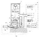
図1は、本発明に係る走査型電子顕微鏡の全体構成の一実施例を示す概念図である。図1に示された走査型電子顕微鏡は、観察対象物(試料)Xに対する電子線Zの照射及び走査等を行う顕微鏡本体部を形成する鏡筒1と、該鏡筒1とは別途独立に配置されており前記電子線Zの照射に伴い前記観察対象物Xから放出される二次電子及び反射電子のそれぞれを検出する二次電子検出器S1及び反射電子検出器S2と、当該鏡筒1内における電子線Zの発生や走査などの電子線制御を指示すると共に、該電子線制御に応じて前記各検出器S1,S2から出力される前記検出した二次電子及び反射電子それぞれに応じた検知信号(検出値など)に基づいて組成像(コンポ像とも呼ぶ)や凹凸像(トポ像とも呼ぶ)などを表示して使用者に提示する制御装置群Aに大きく分けることができる。
FIG. 1 is a conceptual diagram showing an embodiment of the overall configuration of a scanning electron microscope according to the present invention. The scanning electron microscope shown in FIG. 1 includes a
顕微鏡本体部たる鏡筒1は例えば円柱形状をしており、その内部に電子線Zを発生する電子銃2と、前記電子銃2から発生されかつ加速された電子線Zを当該鏡筒1の径方向中心に集束するコンデンサレンズ3及び前記集束後の電子線Z(電子ビーム)を集束且つ偏向制御する走査レンズ部4(なお、この実施形態ではコンデンサレンズ3及び走査レンズ部4が走査偏向手段に該当する)とを含んでなる。上記コンデンサレンズ3は電子レンズであるが、従来装置において用いていた磁場コイルの代わりに永久磁石を用いて構成されてなるものである(後述する図2参照)。また、後述するように走査レンズ部4に含まれる対物レンズ6も、磁場コイルの代わりに永久磁石を用いて構成されてなるものである。
A
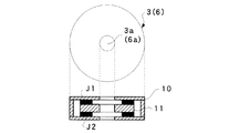
ここで、永久磁石を用いて構成されてなるコンデンサレンズ3(又は対物レンズ6)の一例を図2に示す。図2は、永久磁石を用いて構成されてなるコンデンサレンズ3(又は対物レンズ6)の一実施例を示す断面図である。 Here, FIG. 2 shows an example of the condenser lens 3 (or the objective lens 6) configured using a permanent magnet. FIG. 2 is a cross-sectional view showing an embodiment of the condenser lens 3 (or objective lens 6) formed using a permanent magnet.
図2に示すコンデンサレンズ3(又は対物レンズ6、以下同じ)は、鏡筒1の内径にほぼ一致する大きさの直径を有する円柱形状に形成されてなり、その中央部には電子線Zを通すための中央孔3aを有する。この中央孔3aは磁場解析に応じてシミュレーションされた電子線Zの中心軸が通る位置からの距離に応じた磁束密度の分布に従いその直径の大きさが決められており、当該中央孔3aの範囲内の電子線Zが集束される一方で範囲外の電子線Zは集束されない。すなわち、集束される電子線量は中央孔3aの直径に比例する。このコンデンサレンズ3は、中央部に前記孔3aを有する円板状の2つの永久磁石J1,J2を、それぞれが中央部に前記孔3aを有する断面コの字状の第1コア10と円板状の第2コア11とにより電子線Zの進行方向つまりは鏡筒1の長尺方向に沿って挟みこんだサンドイッチ構造となっている。
A condenser lens 3 (or
ここで、磁場コイルの代わりに永久磁石J1,J2を用いる理由を述べる。一般的に走査型電子顕微鏡により元素分析などを行うには、電子線Zの照射に伴い観察対象物Xから放射されるX線放射量を所定のレベル以上確保する必要がある。そのため、より多くの電子線Zを集束する強力な磁場を前記中心孔3a付近に形成するために磁場コイル(コイル磁石)が用いられていた。しかし、通常の磁場コイルはコアに巻線を多数回巻き付ける構造であることに鑑みると小型化することが非常に難しく、それゆえ鏡筒1を小型化・軽量化するには向いていない。そこで、本実施形態においては磁場コイルに比べて小型化・軽量化しやすい永久磁石J1,J2を用いてコンデンサレンズ3を小型化・軽量化し、これにより鏡筒1自体の小型化・軽量化を実現するようにしている。
Here, the reason why the permanent magnets J1 and J2 are used instead of the magnetic field coil will be described. In general, in order to perform elemental analysis or the like with a scanning electron microscope, it is necessary to secure an X-ray radiation amount radiated from the observation object X with irradiation of the electron beam Z to a predetermined level or more. Therefore, a magnetic field coil (coil magnet) has been used to form a strong magnetic field that focuses more electron beams Z in the vicinity of the central hole 3a. However, in view of the structure in which a normal magnetic field coil has a structure in which a winding is wound many times around a core, it is very difficult to reduce the size, and therefore, it is not suitable for reducing the size and weight of the
ただし、永久磁石J1,J2を用いたコンデンサレンズ3(又は対物レンズ6)では、磁場コイルを用いたものに比べると集束できる電子線Zの量が少ない。そうであるならば、観察対象物Xに対して電子線Zを照射しても元素分析のために必要とされるレベル以上のX線放出量が得られないので元素分析を行うことはできない。そこで、本発明に係る走査型電子顕微鏡は元素分析を行わないもの、つまりは二次電子及び反射電子を利用しての観察用途のみに使用を限定する。用途を限定することにより、観察に必要とされる二次電子及び反射電子を得るのに必要最低限の量の電子線Zを集束できればよいので、コンデンサレンズ3(及び対物レンズ6)は永久磁石J1,J2を用いて構成されてなるものであってよい。 However, in the condenser lens 3 (or objective lens 6) using the permanent magnets J1 and J2, the amount of the electron beam Z that can be focused is smaller than that using the magnetic field coil. If so, even if the observation object X is irradiated with the electron beam Z, the amount of X-ray emission exceeding the level required for the elemental analysis cannot be obtained, so the elemental analysis cannot be performed. Therefore, the scanning electron microscope according to the present invention is limited to an observation application that does not perform elemental analysis, that is, uses secondary electrons and reflected electrons. The condenser lens 3 (and the objective lens 6) is a permanent magnet because it is sufficient to focus the minimum amount of electron beam Z required to obtain secondary electrons and reflected electrons required for observation by limiting the application. It may be configured using J1 and J2.
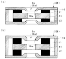
ところで、上記したような永久磁石J1,J2を用いたコンデンサレンズ3の場合、永久磁石J1,J2の特性から磁場コイルが用いられた従来のコンデンサレンズのような磁場制御を電気的に行うことはできない。そこで、本実施形態において用いられるコンデンサレンズ3(又は対物レンズ6)については永久磁石J1,J2や各コア10,11の形状が異なるものを多数用意しておき、これらを必要に応じて交換することで磁場制御を行うことのできるようにしている。そうしたコンデンサレンズ3(又は対物レンズ6)の一例を図3に示す。図3は、永久磁石を用いて構成されてなるコンデンサレンズ3(又は対物レンズ6)の別の実施例を示す断面図である。
By the way, in the case of the
図3(a)に示すコンデンサレンズ3(又は対物レンズ6)は、図2に示したものと比較して断面コの字状の第1コア10の形状が異なっている。ここに示した第1コア10は、中心孔3aに面する側のコア先端部10aが共に断面中央に配置された第2コア11側に曲げられた形状に形成されている。これにより、第1コア10の先端部10aと第2コア20との間隔が狭くなると共に、第1コア10の先端部10aが永久磁石J1,J2に近くなる。他方、図3(b)に示すコンデンサレンズ3(又は対物レンズ6)は、図3(a)に示したものと比較すれば全体形状はほぼ同一であるが、永久磁石J1,J2の厚みを大きくしている。このようにして、永久磁石J1,J2と第1コア10との距離(間隙)を図2に示したものと比較してより近くすることによって、あるいは永久磁石J1,J2をより体積の大きいものにすることによって、より強力な磁場を中心孔3a付近に形成させることができ(磁場制御)、より多くの電子線Zを集束させることができる。
The condenser lens 3 (or objective lens 6) shown in FIG. 3A differs from the one shown in FIG. 2 in the shape of the
図1の説明に戻って、前記コンデンサレンズ3により集束された電子線Z(電子ビーム)は、走査レンズ部4によってその進行方向の向きが偏向制御される。この集束後の電子線Zを偏向制御する走査レンズ部4は、上段側に電子線Zを偏向するための走査コイル5を、下段側に該偏向された電子線Zを絞るための対物レンズ6をそれぞれ配置したものである。勿論、走査レンズ部4,該走査レンズ部4内に配置される走査コイル5及び対物レンズ6の径方向中央には、電子線Zを通すための孔4a,5a,6aがそれぞれ設けてある。そして、この走査コイル5と対物レンズ6とが一体化された走査レンズ部4の視野移動を行うための移動機構として、前記走査レンズ部4を一定の球面体上で移動させるための駆動モータ(図示せず)及び前記球面体等を含んでなる球面座Qを有する。この球面座Qの球面体はその中心点がコンデンサレンズ3の焦点位置(図中G点参照)に一致する曲率に形成されてなり、前記焦点位置Gを基準として走査レンズ部4の下方に配置される。これによれば、前記駆動モータの動作に伴い前記焦点位置Gを基点に、前記走査レンズ部4は鏡筒1の径方向のどの方向にも前記球面上を滑らかに移動する(つまり視野移動する)。したがって、後述するようにして鏡筒1に観察対象物Xを密着固定させた状態で電子線Zを照射するようにした本実施形態においても、観察対象物Xを動かすことなく観察対象物X表面の任意の位置(ただし狭い範囲)に対し電子線Zを照射させることができる。
Returning to the description of FIG. 1, the scanning direction of the electron beam Z (electron beam) focused by the
本実施形態では、従来のビーム偏向のための機構は大型であり鏡筒1の小型化・軽量化に対して実用的でない点を解決するためだけでなく、従来の走査コイルだけによる単なるビーム偏向では偏向時の収差が増大してしまい高い分解能が望めない点を解決するために、ビーム偏向に起因する収差を発生させない特殊な電子光学系として、上記の走査コイル5と対物レンズ6とを一体化した走査レンズ部4からなる電子光学系を採用したうえで、前記走査レンズ部4を移動する機構として球面座Qを用いている。すなわち、この構成によれば、前記球面座Qによる前記走査レンズ部4の移動によってビーム偏向時における対物レンズ6の主面の法線方向を電子線Zの進入方向と合わせることが可能となるので、視野を移動させた場合に現れるビーム偏向に起因する収差をできる限り少なくすることができる。また、電子銃2及びコンデンサレンズ3の光学軸から観察対象物Xに電子線Zを最終的に照射する走査レンズ部4の光学軸を外すことができることから、例えば電子銃2が熱電子放射型電子銃である場合には熱電子カソードの明るさが観察対象物Xまで到達することに起因する観察時に生じ得る悪影響を除去することができる。
In the present embodiment, the conventional mechanism for deflecting the beam is large, not only to solve the point that it is not practical for reducing the size and weight of the
鏡筒1は排出路Pを有してなり、該排出路Pは例えばフレキシブルなチューブ(例えばゴム管など)を介して図示を省略した真空ポンプと接続される。したがって、真空ポンプの動作に伴って前記排出路Pを介して鏡筒1内を満たしていた空気が外部へと排出されて、鏡筒1内部が真空状態に保たれるようになっている。
The
図1から理解できるように、本実施形態における鏡筒1において、電子銃4から発生された電子線Zの進行先の先端部1a側にはそもそも試料室が具えられておらずまた載置台も具えられていない。鏡筒1の先端部1aは単に開口しているだけである。ただし、鏡筒1の開口先端部1aには当該先端部の形状にあわせて形成された環状のシール部材7が設置されている。このシール部材7は弾力のある部材(例えばゴムなど)で形成されてなり、鏡筒1内部と外部との間で空気の出入りができないように鏡筒1と観察対象物Xとを密着させるためのものである。このシール部材7を介して鏡筒1と観察対象物Xとを密着させてから上記したようにして真空ポンプの駆動に伴って鏡筒1内部が真空状態に保たれると、その作用によって鏡筒1に観察対象物Xが吸着されて互いに密着した状態を維持させることができる。したがって、鏡筒1内の真空状態が解除されない限り、鏡筒1と観察対象物Xとは互いに離れることがない。
As can be understood from FIG. 1, in the
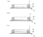
ところで、観察対象物Xの表面の凹凸具合によっては前記シール部材7を介しての鏡筒1と観察対象物Xとの密着度が低いがために、鏡筒1内を真空状態に保ち観察対象物Xを吸着させたとしても鏡筒1と観察対象物Xとが確実に固定されない恐れがある。そこで、観察対象物X表面の凹凸具合ごとに異なる形状のシール部材7を予め用意しておき、これらを観察対象物X表面の凹凸具合に応じて適宜に交換することのできるようになっている。図4は、観察対象物X表面の凹凸具合毎に異なる形状からなるシール部材7の一実施例を示す断面図である。
By the way, depending on the unevenness of the surface of the observation object X, the degree of adhesion between the
図4(a)に示すシール部材7は比較的に滑らかな表面の観察対象物Xとの固定に用いるものであり、当該シール部材7は断面円状部分から円弧部7aが観察対象物Xとの接触側(すなわち観察面側)に突出した形状に形成されてなる。鏡筒1内部の真空状態の進行に応じて、この突出した円弧部7aが押し潰されるように変形する。それにより、前記円弧部7aと観察対象物Xとの接触面がより大きくなるように拡がった状態で鏡筒1に観察対象物Xが吸着され、また円弧部7aと観察対象物X表面との間には隙間がなく鏡筒1内部と外部との間で空気の出入りがない高真空状態に鏡筒1内を保つことができることから、鏡筒1と観察対象物Xとは確実に密着固定される。
The
図4(b)に示すシール部材7は小さな凹凸のある少し粗い表面の観察対象物Xとの固定に用いるものであり、当該シール部材7は観察対象物Xとの接触側(すなわち観察面側)に断面円状部分から鏡筒1の外周側に向かって拡げられるように、また先端部側が薄い押え板部7bを有した形状に形成されてなる。鏡筒1内部の真空状態の進行に応じて、この押え板部7bが観察対象物Xに押し潰されてより外周側へと拡げられるように変形する。それにより、前記押え板部7bと観察対象物Xとの接触面がより大きくなるように拡がった状態で鏡筒1に観察対象物Xが吸着され、また押え板部7bと観察対象物X表面との間には隙間がなく鏡筒1内部と外部との間で空気の出入りがない高真空状態に鏡筒1内を保つことができることから、小さな凹凸のある少し粗い表面の観察対象物Xであっても鏡筒1と観察対象物Xとは確実に密着固定される。
The
図4(c)に示すシール部材は凹凸の大きな粗い表面の観察対象物Xとの固定に用いるものであり、当該シール部材7は観察対象物Xとの接触側(すなわち観察面側)に断面円状部分から鏡筒1の外周側及び内周側それぞれに向かって拡げられるように枝別れした2又の押え板部7cを有した形状に形成されてなる。鏡筒1内部の真空状態の進行に応じて、この押え板部7cが観察対象物Xに押し潰されてより外周側及び内周側へと拡げられるように変形する。それにより、前記枝別れした2又の押え板部7cが観察対象物X表面上の凹凸に沿って密着されるようにして互いの接触面がより大きい状態で鏡筒1に観察対象物Xが吸着され、こうした押え板部7cと観察対象物X表面との間には隙間がなく鏡筒1内部と外部との間で空気の出入りがない高真空状態に鏡筒1内を保つことができることから、凹凸の大きな粗い表面の観察対象物Xであっても鏡筒1と観察対象物Xとは確実に密着固定される。
The seal member shown in FIG. 4C is used for fixing to the observation object X having a rough surface with large irregularities, and the
なお、上記の各シール部材7は必ずしも上記した表面の観察対象物Xとの固定のみに用いることに限らない。例えば、図4(c)に示したシール部材7を、比較的に滑らかな表面の観察対象物Xとの固定や小さな凹凸のある少し粗い表面の観察対象物Xとの固定に用いてもよい。
In addition, each said sealing
観察対象物Xの表面に電子線Zが照射されると、鏡筒1にシール部材7を介して密着固定(詳しくは吸着)されている観察対象物Xから二次電子及び反射電子が放出される。該観察対象物Xから発せられた二次電子及び反射電子は、二次電子検出器S1及び反射電子検出器S2によりそれぞれ検出される。
When the surface of the observation object X is irradiated with the electron beam Z, secondary electrons and reflected electrons are emitted from the observation object X that is closely fixed (specifically adsorbed) to the
前記二次電子検出器S1は、シンチレータ8とライトガイドFと光電子増倍管Mとを含んでなる。そのうちのシンチレータ8は鏡筒1内部に敷設される一方で、前記シンチレータ8とライトガイドFを介して接続される長尺形状の光電子倍増管Mは鏡筒1の側面部に敷設されることなく、鏡筒1と別途独立した状態で鏡筒1の外部に分離配置される。この実施例において、鏡筒1内部に敷設された前記シンチレータ8と鏡筒1外部に分離配置された前記光電子倍増管Mとを接続するライトガイドFとしては、フレキシブルな光ファイバーケーブル(光信号伝送路)が用いられる。フレキシブルな光ファイバーケーブルを用いることで、前記光電子倍増管Mを鏡筒1外部の任意の位置に配置しても観察対象物Xに対する鏡筒1の移動が大きく制限されることのないようにしている。
The secondary electron detector S1 includes a
前記シンチレータ8で取得(受光)された二次電子は、光ファイバーケーブル内を通って光電子倍増管Mへと伝送される。光電子倍増管Mは伝送されてきた二次電子を電気的な検知信号へと変換し、該検知信号を電気的に接続された後述するコントローラ部E(図1参照)に出力する。このように、本実施例においては、長尺形状の光電子倍増管Mを鏡筒1に直接敷設することなく、光電子倍増管Mを鏡筒1外部に分離配置してフレキシブルな光ファイバーケーブルからなるライトガイドFを介して鏡筒1内部に配置されるシンチレータ8と接続するようにしたことにより、鏡筒1を従来のような側面部が大きく突出した形状(図6参照)に形成する必要がないので鏡筒1を小型化できると共に、鏡筒1自体に光電子倍増管Mを支持させなくてよいので鏡筒1の強度が小さくてすむ、つまりは鏡筒1を軽量化できる。
Secondary electrons acquired (received) by the
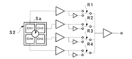
他方、前記反射電子検出器S2は鏡筒1内部において観察対象物Xの直上に位置するように敷設されており、反射電子検出器S2の中央部には走査レンズ部4によってその進行方向の向きが偏向制御された電子線Zを通すための孔Saが設けられている。ここで、前記反射電子検出器S2について図5を用いて説明する。図5は、反射電子検出器の一実施例を示す概念図である。ここに示す反射電子検出器S2は反射電子の検知領域を4分割にした4分割反射電子検出器であって、図示のように電子線Zを通すための孔Saを中心にこれを囲むようにして4分割された検知領域(チャンネルCH1〜CH4)毎に設けられている極性切換チャンネルR1〜R4によって極性「+」,「−」を自由に設定できるようにしてある。例えば、4チャンネルCH1〜CH4全ての極性切換チャンネルR1〜R4を「+」に設定した場合には組成像が表示され、4チャンネルCH1〜CH4のうちの2チャンネル又は1チャンネルの極性切換チャンネル(R1〜R4)を「−」にその他のチャンネルの極性切換チャンネル(R1〜R4)を「+」に設定した場合には凹凸像が表示される。すなわち、図5に示す反射電子検出器S2は、前記極性切換チャンネルR1〜R4の設定に従って組成像(コンポ像)及び凹凸像(トポ像)のいずれをも表示することが可能となっている。当該反射電子検出器S2は検出した反射電子に応じた電気的な検知信号を生成し、該検知信号を信号線L及びコネクタ9を介して電気的に接続された後述するコントローラ部E(図1参照)に出力する。
On the other hand, the backscattered electron detector S2 is laid in the
また、従来では試料の観察対象位置(観察面)を移動する際に電子線Zの中心軸は固定位置であるがゆえに、載置台Oを移動させることによって前記載置台O上の試料を移動させるようにしている。そして載置台Oに取り付けられているファラデーカップにより計測される電子線の強度分布に従い、載置台Oの移動に伴う試料と電子線Zの中心軸との相対的位置を把握するようにしている。しかし、本願発明では載置台Oを具えていない代わりに走査レンズ部4を球面座Qにより移動させることによって電子線Zの偏向制御を行っており、従来あった電子線Zの中心軸を割り出すためのファラデーカップを有していない。そのため、ファラデーカップに代わって走査レンズ部4の移動にあわせて変位する電子線Zの中心軸の位置を正しく把握させるための機構が必要である。
Further, since the central axis of the electron beam Z is a fixed position when moving the observation target position (observation surface) of the sample in the past, the sample on the mounting table O is moved by moving the mounting table O. I am doing so. Then, according to the intensity distribution of the electron beam measured by the Faraday cup attached to the mounting table O, the relative position between the sample and the central axis of the electron beam Z accompanying the movement of the mounting table O is grasped. However, in the present invention, the deflection control of the electron beam Z is performed by moving the
そこで、この実施形態においては、コンデンサレンズ3によって集束された電子線Zの中心軸のある位置を把握してその位置に走査レンズ部4の中心が位置するように調整(つまり光軸調整;センタリング)を行うために、上記した4分割反射電子検出器S2を使用する。その場合、電子線Zを照射することに応じて得られる反射電子が前記分割した4つの各検知領域(チャンネルCH1〜CH4)に均等に分散した状態として検出された場合に、コンデンサレンズ3によって集束された電子線Zの中心軸と一致する位置に走査レンズ部4の中心が正しくセンタリングされたと判定すればよい。
Therefore, in this embodiment, the position of the central axis of the electron beam Z focused by the
ところで、前記球面座Qによる走査レンズ部4の動作に従っての電子線Zの走査だけでは移動範囲が限られることから、観察対象物Xを密着固定した状態のままでは観察可能な範囲が限られる。従来においては試料室内において試料(観察対象物X)は垂直方向及び水平方向に移動可能であってさらには傾斜及び回転可能な載置台O(図6参照)に載せられており、該載置台Oを駆動制御することで試料(観察対象物X)上における大幅な観察位置の変更を行うことのできるようになっていることは既に述べたとおりである。
By the way, since the moving range is limited only by scanning the electron beam Z according to the operation of the
しかし、図1から理解できるように、本願発明に係る装置では鏡筒1の開口先端部側(図中では下方側)にそもそも試料室が具えられておらずまた載置台も具えられていない。本願発明に係る装置では鏡筒1の開口先端部に観察対象物Xを吸着により密着固定させて電子線Zの照射を行うようにしているため、装置自体を観察対象物X上の任意の観察位置に移動させる必要がある。そうするには一旦観察対象物Xから鏡筒1を離す必要が有るが、本発明では鏡筒1と観察対象物Xとは鏡筒1内が高真空状態に保たれることによってシール部材7を介して吸着されているだけであるから、例えば鏡筒1自体を傾けるなどして鏡筒1と観察対象物Xとの密着状態を解除して鏡筒1内に外部から空気を入れてやるようにすれば、鏡筒1内の真空状態が解除されて鏡筒1と観察対象物Xとを離すことができ、鏡筒1を観察対象物Xの任意の位置に観察面を移動することが簡単にできるようになる。
However, as can be understood from FIG. 1, in the apparatus according to the present invention, the sample chamber is not provided on the opening tip side (the lower side in the drawing) of the
上記のようにして真空状態を解除して鏡筒1を観察対象物Xの任意の位置に移動させた場合、観察を行うために再度鏡筒1内を高真空状態にする必要があるのは当然である。その際の時間の削減を目的として、本実施形態では鏡筒1内を2つの部屋100,200に分ける隔壁Hを設けてある。上記隔壁Hの中央部には電子線Zを通すための孔Haが空いている。鏡筒1と真空ポンプ(図示せず)とを繋ぐための上記した排出路Pは、この隔壁Hによって分けられる2つの部屋100,200毎に設けられる。前記2つの部屋100,200のうち鏡筒1の開口先端部1a側(図中では下段側)の部屋200と真空ポンプとを繋ぐ排出路の途中には、遮断扉T(シャッター)が設けてある。
As described above, when the vacuum state is released and the
前記遮断扉Tは鏡筒1と観察対象物Xとを相対的に移動させることのない電子線Zの照射時(つまり観察時)においては排出路Pを開放した状態に制御されるようになっており、上段側の部屋100(第1の部屋)と同様に開口先端部1a側の部屋200(第2の部屋)についても真空ポンプによって高真空状態が保たれるようになっている。他方、前記遮断扉Tは鏡筒1と観察対象物Xとを相対的に移動させる電子線Zが照射されていない時(つまり観察していない時)においては排出路Pを閉鎖した状態に制御されるようになっており、開口先端部1a側の部屋200を上段側の部屋100に比べて低真空状態とすることによって鏡筒1と観察対象物Xとを離しやすくするようにしている。また、鏡筒1内を2つの部屋100,200に分けていることから、鏡筒1を観察対象物1の任意の位置に移動した後に再度鏡筒1内を高真空状態にする際には、上段側の部屋100に比較して低真空状態となった開口先端部1a側の部屋200をできる限り速くに高真空状態とすればよいことから、鏡筒1内を高真空状態にするのに係る時間を節約することができる。
The blocking door T is controlled to be in a state in which the discharge path P is opened at the time of irradiation of the electron beam Z that does not relatively move the
図1の説明に戻って、観察対象物Xに電子線Zを照射するために、上記した鏡筒1内に内装される電子銃2や走査偏向手段(この実施形態ではコンデンサレンズ3及び走査レンズ部4が該当する)に対する制御命令は、制御装置群Sに含まれるコントローラ部Eから行われる。前記コントローラ部Eは例えばCPU、ROM、RAM等を含んでなるコンピュータであって、鏡筒1内における電子線Zの走査に伴う観察対象物X表面への電子線Zの照射を制御するために、電子線制御部B及び走査レンズ部移動制御部Cに対して制御命令を送る。
Returning to the description of FIG. 1, in order to irradiate the observation object X with the electron beam Z, the
前記電子線制御部Bは、コントローラ部Eからの制御命令に従って電子線Zの発生オン/オフを行うよう鏡筒1内の電子銃2を制御する。走査レンズ部移動制御部Cは、コントローラ部Eからの制御命令に従って電子線Zの偏向を行うよう鏡筒1内における球面座Qによる走査レンズ部4の移動操作を行う動作機構を制御する。また、コントローラ部Eは鏡筒1の外部に別途配置されている各検出器S1,S2から検出された二次電子及び反射電子に応じた信号を受信し、該受信した信号に基づいて組成像(コンポ像)や凹凸像(トポ像)などを表示部Dに表示する。使用者は、該表示部Dに表示されたこれらの像を見て観察対象物Xの観察を行うことができる。
The electron beam control unit B controls the
なお、ここでは図示を省略したが、制御装置群Sは各部を動作させるための電源、真空ポンプのオン/オフを制御する真空ポンプ制御部、鏡筒1と真空ポンプとを繋ぐ排出路Pの途中に配置された遮断扉Tの開閉を制御する扉制御部などを含んでいてよい。勿論、上記した以外の制御部など他の構成要素を含んでいてよい。
Although not shown here, the control device group S includes a power source for operating each unit, a vacuum pump control unit that controls on / off of the vacuum pump, and a discharge path P that connects the
以上のように、本実施形態においては鏡筒1の開口先端部1aに観察対象物Xと直接接触するシール部材7を設ける。真空ポンプにより鏡筒1内が真空に引かれると、前記シール部材7が観察対象物Xに接触した状態のまま変形して鏡筒1に当該観察対象物Xを吸着させる。このとき、鏡筒1内及び観察対象物X表面上における真空状態が確保される。前記シール部材7を用いての観察対象物Xの吸着により、前記鏡筒1を観察対象物Xに直接接触させた状態で密着固定することができる。すなわち、従来の走査型電子顕微鏡が有していた閉鎖可能な試料室をなくしたかわりに、観察対象物Xに対して直接鏡筒1の開口先端部1aを吸着させて観察対象物Xと顕微鏡本体部である鏡筒1とが相対的に移動しないように密着固定させる。
As described above, in this embodiment, the
こうすると、試料室のない小型・軽量な鏡筒を有する電子顕微鏡であるにも関わらず、鏡筒1内及び観察対象物X表面上における真空状態を容易に確保することができるし、また鏡筒1あるいは観察対象物X自体が振動したとしても鏡筒1と観察対象物Xとは相対的に移動しないことから画像のぶれ等の観察時の悪影響は生じない。こうして、鏡筒1を観察対象物Xに対し直接マウントして電子線Zを照射できるようにしたので、従来においては試料室に入りきらない大きさの観察対象物Xであっても特に加工を施すことなく現状状態そのままでの観察を行うことができるようになる。
In this way, it is possible to easily ensure a vacuum state in the
二次電子検出器S1を構成するシンチレータ8を鏡筒1内部に配置する一方で、光電子倍増管Mを鏡筒1外部に鏡筒1とは別途独立に分離配置したことから、鏡筒1に直接光電子倍増管Mを敷設する場合に比べて鏡筒1を小型化することができ、また鏡筒1自体に強度が必要とされないことから鏡筒1を軽量化することができる。また、コンデンサレンズ3と対物レンズ6を永久磁石J1,J2を用いて形成したことにより、磁場コイルで形成されたコンデンサレンズ及び対物レンズを用いる場合に比べてコンデンサレンズや対物レンズを小さく形成することができ、それにより鏡筒1自体の小型化・軽量化を図れる。さらには、走査コイル5と対物レンズ6とを一体構成した走査レンズ部4を球面座Qに従って一定の球面上を移動させて、鏡筒1内における電子線Zの進行方向を制御して視野移動させるようにしたので、試料室のない鏡筒1であるにも関わらず、観察対象物X上における大幅な観察位置(観察面)の変更を行うことができる。
While the
また、本願発明に係る走査型電子顕微鏡の鏡筒1は小型・軽量であるので、本装置はアーム部の先端などに取り付けやすく、また開口先端部の向きが下方のみに制限されずにどのような向きであっても観察を行うことができることから、例えば自動車(完成車)全体つまりは自動車の上面、下面、側面などやエンジン内部あるいは室内などに使用されている部材を観察しやすい、という利点がある。
In addition, since the
以上、図面に基づいて実施形態の一例を説明したが、本発明はこれに限定されるものではなく、様々な実施形態が可能であることは言うまでもない。また、本発明は走査型電子顕微鏡の使用目的に限定するものではない。例えば、電子ビーム描画装置にも利用可能である。その他、本発明の要旨を逸脱しない範囲で、種々変形して実施することが可能である。 As mentioned above, although an example of embodiment was demonstrated based on drawing, this invention is not limited to this, It cannot be overemphasized that various embodiment is possible. Further, the present invention is not limited to the intended use of the scanning electron microscope. For example, it can be used for an electron beam drawing apparatus. In addition, various modifications can be made without departing from the scope of the present invention.
1…鏡筒
1a…開口先端部
2…電子銃
3…コンデンサレンズ
4…走査レンズ部
5…走査コイル
6…対物レンズ
7…シール部材
8…シンチレータ
9…コネクタ
10,11…コア
300…試料室
A…制御装置群
B…電子線制御部
C…走査レンズ部移動制御部
D…表示部
E…コントローラ部
F…ライトガイド
H…隔壁
J1,J2…永久磁石
K…開閉扉
L…信号線
M…光電子倍増管
O…載置台
P…排出路
Q…球面座
R1〜R4…極性切換スイッチ
S1…二次電子検出器
S2…反射電子検出器
T…遮断扉
X…試料(観察対象物)
Z…電子線(電子ビーム)
DESCRIPTION OF
Z ... Electron beam (electron beam)
Claims (6)
前記電子銃から発生される電子線を集束する集束レンズと、
前記集束した電子線を偏向する走査コイルと、
前記偏向した電子線の焦点を観察対象物にあわせる対物レンズと、
前記対物レンズを前記走査コイルと共に一体的に移動させる移動機構と、
前記電子線の照射に伴い観察対象物から放出される二次電子を検出する二次電子検出器及び前記電子線の照射に伴い観察対象物から放出される反射電子を検出する反射電子検出器の少なくともいずれか一方と、
前記電子銃から発生された電子線の進行方向側の先端部が開口した鏡筒であって、当該鏡筒内に少なくとも前記電子銃と前記集束レンズと前記走査コイルと前記対物レンズと前記移動機構とを含んでなるものと、
前記鏡筒の開口先端部に設けられ前記観察対象物と接触させるシール部材と、
前記鏡筒内を真空に引くことに従い前記シール部材を介して前記鏡筒に観察対象物を吸着させる真空手段と
を備えてなり、
前記移動機構は、前記対物レンズ及び前記走査コイルを球面体上で移動させるための駆動モータと、前記球面体を形成する球面座とを少なくとも含み、該球面座はその球面体の中心点が前記集束レンズの焦点位置に一致する曲率に形成されてなり、
前記移動機構によって前記対物レンズと前記走査コイルとを一体的に移動することにより、前記鏡筒に観察対象物を吸着させたまま前記鏡筒内における前記電子線の進行方向を制御して視野移動することを特徴とする電子顕微鏡。 An electron gun that generates an electron beam;
A focusing lens for focusing an electron beam generated from the electron gun;
A scanning coil for deflecting the focused electron beam;
An objective lens for focusing the deflected electron beam on the observation object;
A moving mechanism for moving the objective lens together with the scanning coil;
A secondary electron detector that detects secondary electrons emitted from the observation object as a result of irradiation with the electron beam, and a reflected electron detector that detects reflected electrons emitted from the observation object as a result of irradiation with the electron beam. At least one of them,
A lens barrel having an opening on the traveling direction side of an electron beam generated from the electron gun, and at least the electron gun, the focusing lens, the scanning coil, the objective lens, and the moving mechanism in the lens barrel Comprising
A seal member provided at an opening tip of the lens barrel and brought into contact with the observation object;
Vacuum means for adsorbing an observation object to the lens barrel through the seal member according to drawing the inside of the lens barrel to a vacuum;
The moving mechanism includes at least a drive motor for moving the objective lens and the scanning coil on a spherical body, and a spherical seat forming the spherical body, and the spherical seat has a center point of the spherical body as the central point. It is formed with a curvature that matches the focal position of the focusing lens,
By moving the objective lens and the scanning coil integrally by the moving mechanism, the field of view is moved by controlling the traveling direction of the electron beam in the barrel while the observation target is attracted to the barrel. An electron microscope characterized by that.
Priority Applications (3)
| Application Number | Priority Date | Filing Date | Title |
|---|---|---|---|
| JP2010274626A JP5259688B2 (en) | 2010-12-09 | 2010-12-09 | Scanning electron microscope |
| US13/313,606 US8610061B2 (en) | 2010-12-09 | 2011-12-07 | Scanning electron microscope |
| DE102011087955.2A DE102011087955B4 (en) | 2010-12-09 | 2011-12-08 | Scanning electron microscope |
Applications Claiming Priority (1)
| Application Number | Priority Date | Filing Date | Title |
|---|---|---|---|
| JP2010274626A JP5259688B2 (en) | 2010-12-09 | 2010-12-09 | Scanning electron microscope |
Publications (2)
| Publication Number | Publication Date |
|---|---|
| JP2012124052A JP2012124052A (en) | 2012-06-28 |
| JP5259688B2 true JP5259688B2 (en) | 2013-08-07 |
Family
ID=46144852
Family Applications (1)
| Application Number | Title | Priority Date | Filing Date |
|---|---|---|---|
| JP2010274626A Expired - Fee Related JP5259688B2 (en) | 2010-12-09 | 2010-12-09 | Scanning electron microscope |
Country Status (3)
| Country | Link |
|---|---|
| US (1) | US8610061B2 (en) |
| JP (1) | JP5259688B2 (en) |
| DE (1) | DE102011087955B4 (en) |
Families Citing this family (10)
| Publication number | Priority date | Publication date | Assignee | Title |
|---|---|---|---|---|
| US8476585B2 (en) * | 2011-03-02 | 2013-07-02 | Gatan, Inc. | Microtome utilizing a movable knife in a retardation field scanning electron microscope and a retardation field scanning electron microscope including the same |
| JP5759815B2 (en) * | 2011-07-19 | 2015-08-05 | 株式会社日立ハイテクノロジーズ | electronic microscope |
| WO2013192608A1 (en) | 2012-06-22 | 2013-12-27 | Edax, Inc. | Method and apparatus for electron pattern imaging |
| JP6309195B2 (en) * | 2013-02-18 | 2018-04-11 | 株式会社ホロン | Scanning electron microscope and inspection device |
| DE102017123288B4 (en) * | 2017-10-06 | 2019-11-21 | Airbus Defence and Space GmbH | Apparatus and method for testing electronic components |
| JP6669795B2 (en) * | 2018-03-15 | 2020-03-18 | 株式会社ホロン | Scanning electron microscope and inspection equipment |
| CN112349570B (en) * | 2020-11-09 | 2023-09-26 | 宁波工程学院 | A new type of scanning electron microscope |
| US12542253B2 (en) * | 2023-02-28 | 2026-02-03 | ICT Integrated Circuit Testing Gesellschaft für Halbleiterprüftechnik mbH | Charged particle optics, charged particle beam apparatus, and method for scanning a charged particle beam |
| WO2025131453A1 (en) * | 2023-12-18 | 2025-06-26 | Asml Netherlands B.V. | Module and charged particle-optical device |
| EP4576154A1 (en) * | 2023-12-18 | 2025-06-25 | ASML Netherlands B.V. | Source module and charged particle-optical device |
Family Cites Families (19)
| Publication number | Priority date | Publication date | Assignee | Title |
|---|---|---|---|---|
| FR2316035A1 (en) | 1975-07-02 | 1977-01-28 | Sciaky Sa | ELECTRONIC HARNESS VACUUM MACHINING PLANT |
| JPS5632656A (en) * | 1979-08-23 | 1981-04-02 | Mitsubishi Heavy Ind Ltd | Scanning electron microscope device |
| CS267642B1 (en) | 1987-12-18 | 1990-02-12 | Josef Ing Melkes | Portable rastering electron microscope |
| JPH04349964A (en) | 1991-02-06 | 1992-12-04 | Toshiba Lighting & Technol Corp | Solution coating device |
| JPH06215716A (en) * | 1993-01-18 | 1994-08-05 | Hitachi Ltd | Scanning electron microscope |
| JPH07142022A (en) * | 1993-11-19 | 1995-06-02 | Hitachi Ltd | Focused ion beam device and charged particle detector |
| SG74599A1 (en) | 1997-09-27 | 2000-08-22 | Inst Of Material Res & Enginee | Portable high resolution scanning electron microscope column using permanent magnet electron lenses |
| JP4473964B2 (en) * | 2000-10-18 | 2010-06-02 | エフ・イ−・アイ・カンパニー | FIB column |
| JP4372339B2 (en) * | 2000-12-28 | 2009-11-25 | 株式会社島津製作所 | Irregular image forming apparatus and electron beam analyzer |
| US6797953B2 (en) * | 2001-02-23 | 2004-09-28 | Fei Company | Electron beam system using multiple electron beams |
| JP2004031207A (en) * | 2002-06-27 | 2004-01-29 | Canon Inc | Electron beam irradiation device and scanning electron microscope device |
| NL1023260C1 (en) | 2003-04-24 | 2004-10-27 | Fei Co | Particle-optical device with a permanent magnetic lens and an electrostatic lens. |
| JP4349964B2 (en) | 2003-09-10 | 2009-10-21 | 株式会社日立ハイテクノロジーズ | Small electron gun |
| NL1026006C2 (en) | 2004-04-22 | 2005-10-25 | Fei Co | Particle-optical device provided with lenses with permanent magnetic material. |
| WO2007083756A1 (en) * | 2006-01-20 | 2007-07-26 | Juridical Foundation Osaka Industrial Promotion Organization | Liquid medium for preventing charge-up in electron microscope and method of observing sample using the same |
| JP4795847B2 (en) * | 2006-05-17 | 2011-10-19 | 株式会社日立ハイテクノロジーズ | Electron lens and charged particle beam apparatus using the same |
| CZ2007510A3 (en) | 2007-07-30 | 2008-01-30 | Tescan, S. R. O. | Device for spatial, real time representation of a sample |
| JP2010274626A (en) | 2009-06-01 | 2010-12-09 | Pilot Ink Co Ltd | Applicator |
| CN102859429B (en) * | 2010-04-19 | 2016-05-11 | 西铁城控股株式会社 | Lens before edging and method for manufacturing edging lens |
-
2010
- 2010-12-09 JP JP2010274626A patent/JP5259688B2/en not_active Expired - Fee Related
-
2011
- 2011-12-07 US US13/313,606 patent/US8610061B2/en not_active Expired - Fee Related
- 2011-12-08 DE DE102011087955.2A patent/DE102011087955B4/en not_active Expired - Fee Related
Also Published As
| Publication number | Publication date |
|---|---|
| JP2012124052A (en) | 2012-06-28 |
| US20120145899A1 (en) | 2012-06-14 |
| US8610061B2 (en) | 2013-12-17 |
| DE102011087955A1 (en) | 2012-06-14 |
| DE102011087955B4 (en) | 2019-06-19 |
Similar Documents
| Publication | Publication Date | Title |
|---|---|---|
| JP5259688B2 (en) | Scanning electron microscope | |
| JP3776887B2 (en) | Electron beam equipment | |
| JP6814282B2 (en) | Charged particle beam device | |
| JP2002042713A (en) | Scanning electron microscope with detector in objective lens | |
| JP4354197B2 (en) | Scanning electron microscope | |
| JP2004031207A (en) | Electron beam irradiation device and scanning electron microscope device | |
| US11640897B2 (en) | Charged particle beam device | |
| JP2008198471A (en) | Charged particle beam equipment | |
| JP2012169091A (en) | Scanning electron microscope | |
| JP2003151484A (en) | Scanning charged particle beam device | |
| US20180218877A1 (en) | Imaging device for imaging an object and for imaging a structural unit in a particle beam apparatus | |
| JP4621097B2 (en) | Electron beam apparatus and control method thereof | |
| JP2002324510A (en) | Scanning electron microscope | |
| JP4988308B2 (en) | Gas amplification type detector and electron beam application apparatus using the same | |
| WO2021001935A1 (en) | Charged particle beam device | |
| JP2001006591A (en) | Charged particle beam equipment | |
| US4121100A (en) | Electron microscope | |
| JP5896870B2 (en) | Scanning electron microscope | |
| JP4146103B2 (en) | Electron beam apparatus equipped with a field emission electron gun | |
| JP7604603B1 (en) | Objective lens and charged particle beam device including same | |
| JP4079503B2 (en) | Analytical electron microscope | |
| JP4365765B2 (en) | Electron gun and electron beam device | |
| JP7307768B2 (en) | Scanning electron microscope and objective lens | |
| JP5210088B2 (en) | Electron beam equipment | |
| JPH11154478A (en) | Electron microscope equipment |
Legal Events
| Date | Code | Title | Description |
|---|---|---|---|
| A977 | Report on retrieval |
Free format text: JAPANESE INTERMEDIATE CODE: A971007 Effective date: 20121019 |
|
| A131 | Notification of reasons for refusal |
Free format text: JAPANESE INTERMEDIATE CODE: A131 Effective date: 20121030 |
|
| A521 | Request for written amendment filed |
Free format text: JAPANESE INTERMEDIATE CODE: A523 Effective date: 20121221 |
|
| A131 | Notification of reasons for refusal |
Free format text: JAPANESE INTERMEDIATE CODE: A131 Effective date: 20130129 |
|
| A521 | Request for written amendment filed |
Free format text: JAPANESE INTERMEDIATE CODE: A523 Effective date: 20130228 |
|
| TRDD | Decision of grant or rejection written | ||
| A01 | Written decision to grant a patent or to grant a registration (utility model) |
Free format text: JAPANESE INTERMEDIATE CODE: A01 Effective date: 20130416 |
|
| A61 | First payment of annual fees (during grant procedure) |
Free format text: JAPANESE INTERMEDIATE CODE: A61 Effective date: 20130424 |
|
| FPAY | Renewal fee payment (event date is renewal date of database) |
Free format text: PAYMENT UNTIL: 20160502 Year of fee payment: 3 |
|
| R150 | Certificate of patent or registration of utility model |
Ref document number: 5259688 Country of ref document: JP Free format text: JAPANESE INTERMEDIATE CODE: R150 Free format text: JAPANESE INTERMEDIATE CODE: R150 |
|
| LAPS | Cancellation because of no payment of annual fees |