JP5259082B2 - Concordance verification method and apparatus - Google Patents
Concordance verification method and apparatus Download PDFInfo
- Publication number
- JP5259082B2 JP5259082B2 JP2006344975A JP2006344975A JP5259082B2 JP 5259082 B2 JP5259082 B2 JP 5259082B2 JP 2006344975 A JP2006344975 A JP 2006344975A JP 2006344975 A JP2006344975 A JP 2006344975A JP 5259082 B2 JP5259082 B2 JP 5259082B2
- Authority
- JP
- Japan
- Prior art keywords
- result
- verification
- assertion
- fpga
- assertion check
- Prior art date
- Legal status (The legal status is an assumption and is not a legal conclusion. Google has not performed a legal analysis and makes no representation as to the accuracy of the status listed.)
- Expired - Fee Related
Links
Images
Landscapes
- Tests Of Electronic Circuits (AREA)
- Test And Diagnosis Of Digital Computers (AREA)
- Devices For Executing Special Programs (AREA)
Description
この発明は、半導体集積回路の設計検証を行うHDL機能シミュレーションでの動作結果と当該HDLで記述した半導体集積回路を搭載したFPGAの実機動作結果との一致性を確認する一致検証方法及び装置に関するものである。 The present invention relates to a coincidence verification method and apparatus for confirming the coincidence between an operation result in an HDL function simulation for performing design verification of a semiconductor integrated circuit and an actual operation result of an FPGA on which the semiconductor integrated circuit described in the HDL is mounted. It is.
FPGA(Field Programmable Gate Array)は、書き換え可能なハードウェアを提供するLSI(大規模半導体集積回路)であり、このハードウェアに用途(ユーザ)が要求する機能を実現するデジタル回路である半導体集積回路を搭載することで、ASIC(Application Specific Integrated Circuit:特定用途向けIC)として多用されている。 An FPGA (Field Programmable Gate Array) is an LSI (Large-Scale Semiconductor Integrated Circuit) that provides rewritable hardware, and a semiconductor integrated circuit that is a digital circuit that realizes a function required by a user (user) for this hardware. Is widely used as an ASIC (Application Specific Integrated Circuit).
このFPGAへの半導体集積回路の搭載は、一般に、次のような手順で行われる。すなわち、まず、用途(ユーザ)が要求する機能を実現する半導体集積回路の全体をシステムとして捉えて動作を定義するシステム設計を行い、その定義した各動作を記述した動作レベル記述を作成する。次に、作成した動作レベル記述を、HDL(Hardware Description Language:回路記述言語)を用いて、回路の設計データとなるRTL(Register Transfer Level)記述に変換する。そして、論理合成ツールを用いて、そのRTL記述をゲートレベル記述(ゲートレベル論理回路;ネットリスト)に自動変換する機能・論理設計を行い、生成されたネットリストに基づきレイアウト設計を行う。このようにして得られた半導体集積回路のHDLモデルをFPGAに書き込むことで、所望の半導体集積回路が実装されたLSIであるFPGAが得られる。 Generally, the semiconductor integrated circuit is mounted on the FPGA in the following procedure. That is, first, a system design that defines an operation by regarding the entire semiconductor integrated circuit that realizes a function required by a user (user) as a system is designed, and an operation level description that describes each defined operation is created. Next, the created behavior level description is converted into an RTL (Register Transfer Level) description, which is circuit design data, using HDL (Hardware Description Language). Then, using a logic synthesis tool, a function / logic design for automatically converting the RTL description into a gate level description (gate level logic circuit; net list) is performed, and a layout design is performed based on the generated net list. By writing the HDL model of the semiconductor integrated circuit thus obtained in the FPGA, an FPGA which is an LSI on which a desired semiconductor integrated circuit is mounted can be obtained.
以上のような半導体集積回路の設計では、上記した各設計過程での設計の正当性を調べる設計検証が行われる。この設計検証には、例えば、各設計過程での変換処理が正しいか否かを検証する等価性検証と、各記述が設計対象を正しく表現しているか否かを検証する仕様検証とがある。 In the design of the semiconductor integrated circuit as described above, design verification is performed to check the validity of the design in each design process described above. This design verification includes, for example, equivalence verification for verifying whether conversion processing in each design process is correct, and specification verification for verifying whether each description correctly represents a design object.
従来、この等価性検証を行う装置として、例えば、機能レベルのHDLによるハードウェア記述で表現された論理回路と、ゲートレベルのHDLによるハードウェア記述で表現された上記と同じ論理回路との論理の等価性の検証を行う場合に、プール式の比較による論理検証と、テストパターンを使用した比較シミュレーションによる論理検証とのいずれを使用するかを、論理回路を分割して得られる個々の部分回路ごとに切り分けることによって行う論理検証装置などが提案されている(例えば、特許文献1参照)。 Conventionally, as an apparatus for performing this equivalence verification, for example, a logical circuit between a logic circuit expressed by a hardware description in function level HDL and a logic circuit same as the above expressed in a hardware description by gate level HDL is used. For each partial circuit obtained by dividing the logic circuit, whether to use logic verification by comparison of pool expressions or logic verification by comparison simulation using a test pattern when checking equivalence There has been proposed a logic verification device or the like that is performed by dividing into two (see, for example, Patent Document 1).
また、仕様検証を行う方法として、例えば、仕様に基づく回路動作をPSL(Property Specification Language)などの専用言語(アサーション言語)を用いて定義し、これに違反する動作が検出された場合に警告を発する仕組みであるアサーションチェックをHDLによる論理回路に対して設定し、仕様に違反する動作の有無をチェックする方法が用いられる。なお、アサーションチェックは、回路仕様などに基づいて、専用のマニュアルで作成されており、一種の回路又は組み込みソフトウェアの一部として、RTL設計やソフトウェア中に組み込まれる(例えば、特許文献2参照)。 Also, as a method of performing specification verification, for example, a circuit operation based on the specification is defined using a dedicated language (assertion language) such as PSL (Property Specification Language), and a warning is issued when an operation that violates this is detected. A method is used in which an assertion check, which is a mechanism to be issued, is set for a logic circuit using HDL, and an operation that violates the specification is checked. The assertion check is created in a dedicated manual based on circuit specifications and the like, and is incorporated into RTL design and software as part of a kind of circuit or embedded software (see, for example, Patent Document 2).
しかしながら、HDLによるRTL記述と、当該RTL記述から自動変換されたネットリストを実装したFPGAとの間で動作上の一致性を確認する場合に、従来では、RTL記述のHDL機能シミュレーション出力値と、実機検証におけるFPGA出力値とを別々の検証システムで取得し、両者を比較するようにしているので、出力値の全比較に時間的コストが掛かるという問題がある。 However, when confirming the operational consistency between the RTL description in HDL and the FPGA on which the netlist automatically converted from the RTL description is mounted, conventionally, the HDL function simulation output value of the RTL description, Since the FPGA output values in the actual machine verification are acquired by separate verification systems and compared with each other, there is a problem that it takes time cost for all comparison of output values.
また、上記した従来の一致検証方法では、実機検証で観測できるのはFPGAの出力信号のみであり、FPGAの回路内部で起こる動作の不一致は検出できない。さらに、等価性検証方式においては、半導体集積回路の大規模化に伴い、回路全体の一括した等価性保証が不可能になっているという問題がある。 Further, in the conventional matching verification method described above, only the output signal of the FPGA can be observed in the actual machine verification, and an operation mismatch occurring inside the FPGA circuit cannot be detected. Furthermore, in the equivalence checking method, there is a problem that it is impossible to guarantee the equivalence of the entire circuit as the semiconductor integrated circuit becomes larger.
この発明は、上記に鑑みてなされたものであり、HDL機能シミュレーション結果とFPGAの実機動作結果との一致検証の実行時間を減少可能とし、かつ回路内部の動作不一致も検出できる一致検証方法及び装置を得ることを目的とする。 The present invention has been made in view of the above, and a matching verification method and apparatus capable of reducing the execution time of matching verification between an HDL function simulation result and an actual operation result of an FPGA and detecting an operation mismatch in a circuit. The purpose is to obtain.
上述した目的を達成するために、この発明は、設計した半導体集積回路のHDLモデルの機能シミュレーションでの動作結果と前記HDLモデルを搭載したFPGAの実機検証での動作結果との一致性を検証する一致検証方法であって、(a)前記機能シミュレーションでのシミュレーション動作が前記半導体集積回路の仕様通りであるか否かをアサーションチェック機能を用いて検証する工程と、(b)前記(a)の工程でのアサーションチェック機能によるアサーションチェックの結果履歴を抽出する工程と、(c)前記HDLモデルとともに前記アサーションチェック機能を前記FPGA上に搭載するための論理合成処理及びマッピング処理を実施する工程と、(d)前記(c)の工程にてHDLモデルを搭載した前記FPGAの実機検証での実機動作が仕様通りであるか否かを前記(c)の工程にて当該FPGA上に搭載した前記アサーションチェック機能を用いて検証する工程と、(e)前記(d)の工程での実機検証における前記アサーションチェック機能によるアサーションチェックの結果履歴を抽出する工程と、(f)前記(b)の工程で得られたアサーションチェック結果履歴と前記(e)の工程で得られたアサーションチェック結果履歴とを比較処理し、得られた差異を一致検証結果としてレポート出力する工程とを含むことを特徴とする。 In order to achieve the above-described object, the present invention verifies the consistency between the operation result in the functional simulation of the HDL model of the designed semiconductor integrated circuit and the operation result in the actual machine verification of the FPGA equipped with the HDL model. (A) a step of verifying whether or not the simulation operation in the functional simulation is in accordance with the specifications of the semiconductor integrated circuit using an assertion check function; and (b) in (a) A step of extracting a result history of the assertion check by the assertion check function in the step; and (c) performing a logic synthesis process and a mapping process for mounting the assertion check function on the FPGA together with the HDL model; (D) The actual FPGA equipped with the HDL model in the step (c) Verifying whether the actual machine operation in the certificate conforms to the specification using the assertion check function mounted on the FPGA in the step (c), and (e) in the step (d) A process of extracting the result history of the assertion check by the assertion check function in the actual machine verification, (f) the assertion check result history obtained in the process (b) and the assertion check obtained in the process (e) And a process of comparing the result history and outputting a report of the obtained difference as a matching verification result.
この発明によれば、設計した半導体集積回路のHDLモデルとともにアサーションチェック機能をFPGAに搭載するので、HDLモデルの機能シミュレーション結果に含ませたアサーションチェック結果と、HDLモデルを実装したFPGA上での実機動作結果に含ませたアサーションチェック結果とを用いて双方の動作上の一致検証を行うことができる。したがって、従来行われていた全出力比較による一致検証と比較して、一致検証の実行時間を減少させることが可能になる。また、外部信号のみならず、内部信号も動きの一致検証が行えるので、一致検証精度の向上を図ることができる。 According to the present invention, since the assertion check function is mounted on the FPGA together with the designed HDL model of the semiconductor integrated circuit, the assertion check result included in the function simulation result of the HDL model and the actual machine on the FPGA on which the HDL model is mounted. Using the assertion check result included in the operation result, it is possible to verify the coincidence of both operations. Therefore, it is possible to reduce the execution time of the matching verification as compared with the matching verification by the all output comparison which has been conventionally performed. In addition, not only the external signal but also the internal signal can be subjected to motion matching verification, so that the accuracy of matching verification can be improved.
この発明によれば、HDL機能シミュレーション結果とFPGA実機動作結果との一致検証の実行時間を減少可能とし、かつ回路内部の動作不一致も検出して一致検証精度の向上を図ることができるという効果を奏する。 According to the present invention, it is possible to reduce the execution time of matching verification between the HDL function simulation result and the FPGA actual machine operation result, and to detect the operation mismatch in the circuit and improve the matching verification accuracy. Play.
以下に図面を参照して、この発明にかかる一致検証方法及び装置の好適な実施の形態を詳細に説明する。 Exemplary embodiments of a matching verification method and apparatus according to the present invention will be described below in detail with reference to the drawings.
実施の形態1.
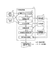
図1は、この発明の実施の形態1による一致検証方法を実施する一致検証装置の構成を示すブロック図である。図1において、HDL機能シミュレーション結果とFPGA上での実機動作結果との間での一致検証を行う一致検証装置1aは、機能シミュレーション部2と、シミュレーション結果抽出部3と、FPGA合成部4aと、実機検証部5と、実機検証結果抽出部6と、実行結果比較部7と、これらの各構成要素での処理データの入出力や保持に用いる記憶部8〜13とを備えている。
FIG. 1 is a block diagram showing a configuration of a coincidence verification apparatus that implements a coincidence verification method according to
記憶部8には、「HDLデザイン記述」が保持されている。この「HDLデザイン記述」は、Verilog−HDLなどのHDLを用いて記述されたRTLの回路設計データであり、機能シミュレーション部2とFPGA合成部4aとが用いる。
The storage unit 8 holds “HDL design description”. This “HDL design description” is RTL circuit design data described using HDL such as Verilog-HDL, and is used by the
記憶部9には、「アサーション記述」が保持されている。「アサーション記述」は、PSLなどのアサーション言語を用いて記述されたアサーションチェックのための回路仕様記述である。アサーション記述には、回路の内部信号及び外部信号が守るべき規則、例えば、信号同士の相互排他関係、バス信号のとり得る値の範囲、または、信号変化が発生するタイミングなどが記述されている。このアサーション記述は、機能シミュレーション部2とFPGA合成部4aとを用いる。
The storage unit 9 holds “assertion description”. The “assertion description” is a circuit specification description for an assertion check described using an assertion language such as PSL. The assertion description describes rules to be observed by the internal signal and external signal of the circuit, such as mutual exclusion relationship between signals, a range of values that can be taken by the bus signal, or timing when a signal change occurs. This assertion description uses the
機能シミュレーション部2は、記憶部8からHDLデザイン記述を、記憶部9からアサーション記述をそれぞれ読み込み、アサーションチェックを含むHDL機能シミュレーションを行うことによって、設計した半導体集積回路の機能検証を行い、その検証結果をシミュレーション結果抽出部3に与える。このように、機能シミュレーション部2は、アサーションチェック可能なシミュレーション装置(シミュレータ)である。
The
シミュレーション結果抽出部3は、機能シミュレーション部2にて実行されたアサーションチェックを含むHDL機能シミュレーションの結果から、「シミュレーション結果履歴」を抽出し、外部ファイルまたはデータベースである記憶部10に保存する。なお、記憶部10に保存される「シミュレーション結果履歴」は、実行結果比較部7が読み込むことができる形式になっている。
The simulation
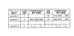
記憶部10に保存される「シミュレーション結果履歴」を、シミュレーション結果履歴10と略記すると、このように抽出されたシミュレーション結果履歴10は、例えば図2に示すように、アサーションチェックの実行結果を含んでいる。アサーションチェックの実行結果には、不合格となったアサーションに関する情報と合格となったアサーションに関する情報とがある。シミュレーション結果履歴10には、不合格となったアサーションに関する情報だけを含む形式でもよく、合格となったアサーションに関する情報だけを含む形式でもよいが、図2では、双方を含む形式で示してある。すなわち、図2では、不合格となったアサーション及び合格となったアサーションを特定するための「アサーション識別子」「不合格が発生した回数」「不合格が発生した時刻に関する情報」「合格が発生した回数」「合格が発生した時刻に関する情報」が示されている。
When the “simulation result history” stored in the
FPGA合成部4aは、記憶部8からHDLデザイン記述を、記憶部9からアサーション記述をそれぞれ読み込み、両者を特定のFPGAデバイス上に実装するための論理合成及びマッピングを行う。すなわち、記憶部8から読み込んだHDLデザイン記述は、半導体集積回路のシステム仕様を実現するデザイン回路としてFPGA内に埋め込まれる。また、記憶部9から読み込んだアサーション記述は、テスト回路としてFPGA内に埋め込まれる。論理合成処理及びマッピング処理の結果は、「合成結果」として記憶部11に保持される。
The
実機検証部5は、記憶部11から合成結果を読込み、FPGA合成部4aにてデザイン回路とともにアサーションチェック用のテスト回路が埋め込まれたFPGA上で実機検証を行う。つまり、実機検証部5では、実機検証を行うことで、アサーションチェックが実行される。このように、実機検証部5は、FPGAが搭載された評価ボードとその実機検証を行うための実行環境になっている。
The real
実機検証結果抽出部6は、実機検証部5にて実行されたアサーションチェックを含む実機検証の結果から、実機検証結果履歴を抽出し、外部ファイルまたはデータベースである記憶部12に保存する。なお、記憶部12に保存される実機検証結果履歴は、実行結果比較部7が読み込むことができる形式になっている。
The real machine verification result extraction unit 6 extracts the real machine verification result history from the result of the real machine verification including the assertion check executed by the real
記憶部12に保存される実機検証結果履歴を、実機検証結果履歴12と略記すると、このように抽出された実機検証結果履歴12は、実機検証でのアサーションチェックの実行結果を含んでいる。実機検証結果履歴12に含まれる実機検証でのアサーションチェックの実行結果は、シミュレーション結果履歴10に含まれるHDL機能シミュレーションでのアサーションチェックの実行結果と同様である。つまり、実機検証結果履歴12には、シミュレーション結果履歴10と同様に、不合格となったアサーションに関する情報と合格となったアサーションに関する情報との一方または双方が含まれている。双方を含む開式で図に示すと、前記した図2に示すようになる。
When the actual machine verification result history stored in the
実行結果比較部7は、シミュレーション結果履歴10と実機検証結果履歴12とを読込み、両者が有するアサーションに関する情報毎に比較を行い、HDL機能シミュレーションの結果とFPGA上での実機動作結果とに一致があるか、不一致があるかを検証し、検証結果を一致検証結果として記憶部13に出力する。この一致検証結果には、比較結果、差異が発見されなかった場合は一致していることを示す情報が含まれ、差異が発見された場合は不一致のあるアサーションの識別子とともに、差異が発生している時刻に関する情報などが含まれている。
The execution result comparison unit 7 reads the
このとき、実行結果比較部7は、比較結果を特定の条件によってフィルタリングする機能を有してもよい。例えば、シミュレーション結果履歴10及び実機検証結果履歴12中の不合格したアサーションについてのみ比較結果を出力したり、特定の時刻に発生する不一致を比較結果から除外したり、もしくは、特定回数以上発生した不一致のみを出力したりするフィルタリング機能を有してもよい。こうしたフィルタリングを通した結果が一致検証結果として記憶部13に保持される。
At this time, the execution result comparison unit 7 may have a function of filtering the comparison result according to a specific condition. For example, a comparison result is output only for failed assertions in the
FPGAに搭載する半導体集積回路(LSI)の設計者は、記憶部13から一致検証結果を読み出すことで、半導体集積回路についてのHDL機能シミュレーション結果とその半導体集積回路を実装したFPGA上での実機動作結果との間に致命的な不一致動作が存在するか否か確認することができる。ここでの確認には、外部信号のみならず、内部信号の動きの確認も含まれている。
The designer of the semiconductor integrated circuit (LSI) mounted on the FPGA reads out the coincidence verification result from the
以上のように、この実施の形態1によれば、FPGAにもアサーションチェックを搭載するので、半導体集積回路についてのHDL機能シミュレーション結果に含ませたアサーションチェック結果と、その半導体集積回路を実装したFPGA上での実機動作結果に含ませたアサーションチェック結果とを用いて双方の動作上の一致検証が行える。 As described above, according to the first embodiment, since the assertion check is also mounted on the FPGA, the assertion check result included in the HDL function simulation result for the semiconductor integrated circuit and the FPGA on which the semiconductor integrated circuit is mounted. By using the assertion check result included in the actual machine operation result above, it is possible to verify the coincidence of both operations.
したがって、従来行われていた全出力比較による一致検証と比較して、一致検証の実行時間を減少させることが可能になる。また、外部信号のみならず、内部信号も動きの一致検証が行えるので、一致検証精度の向上を図ることができる。 Therefore, it is possible to reduce the execution time of the matching verification as compared with the matching verification by the all output comparison which has been conventionally performed. In addition, not only the external signal but also the internal signal can be subjected to motion matching verification, so that the accuracy of matching verification can be improved.
実施の形態2.
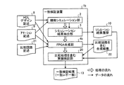
図3は、この発明の実施の形態2による一致検証方法を実施する一致検証装置の構成を示すブロック図である。なお、図3では、図1(実施の形態1)に示した構成要素と同一ないしは同等である構成要素には同一の符号が付されている。ここでは、この実施の形態2に関わる部分を中心に説明する。
FIG. 3 is a block diagram showing the configuration of a coincidence verification apparatus that implements the coincidence verification method according to
図3に示すように、この実施の形態2による一致検証装置1bは、図1(実施の形態1)に示した構成において、FPGA合成部4aに代えてFPGA合成部4bが設けられ、FPGA合成部4bが用いる「比較回路記述」の記憶部21が追加され、記憶部11に代えてFPGA合成部4bが出力する「比較回路を含む合成結果」の記憶部22が設けられている。
As shown in FIG. 3, in the configuration shown in FIG. 1 (Embodiment 1), the matching
そして、図1(実施の形態1)に示した構成において、実機検証部3,実機検証結果抽出部6及び実行結果比較部7に代えて比較処理を含む実機検証部20が設けられ、「実機検証結果履歴」の記憶部11は削除されている。つまり、この比較処理を含む実機検証部20は、図1(実施の形態1)に示した構成において、実機検証結果抽出部6と実行結果比較部7とを実機検証部5の中に取り込んだ構成を有していると言える。
In the configuration shown in FIG. 1 (Embodiment 1), an actual
記憶部21に保持され「比較回路記述」は、図1(実施の形態1)における実機検証結果抽出部6と実行結果比較部7とを実現するRTLの比較回路記述である。
The “comparison circuit description” held in the
FPGA合成部4bは、記憶部8からHDLデザイン記述を、記憶部9からアサーション記述を、記憶部21から比較回路記述をそれぞれ読み込み、三者を特定のFPGAデバイス上に実装するための論理合成及びマッピングを行う。論理合成処理及びマッピング処理の結果は、「比較回路を含む合成結果」として記憶部22に保持される。
The
比較処理を含む実機検証部20は、シミュレーション結果履歴10と記憶部22の「比較回路を含む合成結果」とを読み込み、FPGA実機検証処理と、実機検証結果の抽出処理と、シミュレーション結果履歴10とFPGA実機検証結果との間の実行結果比較処理との全てをFPGA上で実行する。
The actual
ここで、実機検証処理は、実施の形態1にて説明した実機検証部5での処理と同様である。実機検証結果の抽出処理は、実施の形態1にて説明した実機検証結果抽出部6と同様の処理をFPGA上で実機検証処理と平行して実行する。シミュレーション結果履歴10とFPGA実機検証結果との間の実行結果比較処理は、比較内容については実施の形態1にて説明した実行結果比較部7と同様である。比較処理の手順としては、比較処理の必要に応じて記憶部10から「シミュレーション結果履歴」をFPGA内に読み込み、FPGA内で抽出される実機検証結果と比較して「一致検証結果」を記憶部13に出力する。
Here, the actual machine verification process is the same as the process in the actual
以上のように、この実施の形態2によれば、HDL機能シミュレーション結果とFPGA実機動作結果との比較処理がFPGA内に実装して実行されるので、実施の形態1と比べて「一致検証結果」の出力までの処理時間が短縮される。 As described above, according to the second embodiment, the comparison process between the HDL function simulation result and the FPGA actual machine operation result is implemented and executed in the FPGA. The processing time until the output of "is shortened.
以上のように、この発明にかかる一致検証方法及び装置は、設計した半導体集積回路のHDLモデルの機能シミュレーションでの動作結果と前記HDLモデルを搭載したFPGAの実機検証での動作結果との一致性を検証する実行時間を短くするとともに、回路内部の動作不一致も検出して一致検証精度の向上を図るのに有用である。 As described above, the coincidence verification method and apparatus according to the present invention is consistent between the operation result of the functional simulation of the HDL model of the designed semiconductor integrated circuit and the operation result of the actual machine verification of the FPGA equipped with the HDL model. This is useful for shortening the execution time for verifying and detecting the operation mismatch in the circuit and improving the matching verification accuracy.
1a,1b 一致検証装置
2 機能シミュレーション部
3 シミュレーション結果抽出部
4a,4b FPGA合成部
5 実機検証部
6 実機検証結果抽出部
7 実行結果比較部
8 HDLデザイン記述の記憶部
9 アサーション記述の記憶部
10 シミュレーション結果履歴の記憶部
11 合成結果の記憶部
12 実機検証結果履歴の記憶部
13 一致検証結果の記憶部
20 比較処理を含む実機検証部
21 比較回路記述の記憶部
22 比較回路を含む合成結果の記憶部
DESCRIPTION OF
Claims (10)
(a)前記機能シミュレーションでのシミュレーション動作が前記半導体集積回路の仕様通りであるか否かをアサーションチェック機能を用いて検証する工程と、
(b)前記(a)の工程でのアサーションチェック機能によるアサーションチェックの結果履歴を抽出する工程と、
(c)前記HDLモデルとともに前記アサーションチェック機能を前記FPGA上に搭載するための論理合成処理及びマッピング処理を実施する工程と、
(d)前記(c)の工程にてHDLモデルを搭載した当該FPGAの実機検証での実機動作が仕様通りであるか否かを前記(c)の工程にて当該FPGA上に搭載した前記アサーションチェック機能を用いて検証する工程と、
(e)前記(d)の工程での実機検証における前記アサーションチェック機能によるアサーションチェックの結果履歴を抽出する工程と、
(f)前記(b)の工程で得られたアサーションチェック結果履歴と前記(e)の工程で得られたアサーションチェック結果履歴とを比較処理し、得られた差異を一致検証結果としてレポート出力する工程と
を含むことを特徴とする一致検証方法。 A matching verification method for verifying a match between an operation result in a functional simulation of an HDL model of a designed semiconductor integrated circuit and an operation result in an actual machine verification of an FPGA equipped with the HDL model,
(A) verifying, using an assertion check function, whether the simulation operation in the functional simulation is in accordance with the specifications of the semiconductor integrated circuit;
(B) a step of extracting the result history of the assertion check by the assertion check function in the step (a);
(C) performing logic synthesis processing and mapping processing for mounting the assertion check function on the FPGA together with the HDL model;
(D) The assertion mounted on the FPGA in the step (c) whether or not the actual machine operation in the actual machine verification of the FPGA mounted with the HDL model in the step (c) is as specified. A verification process using a check function;
(E) extracting a result history of the assertion check by the assertion check function in the actual machine verification in the step (d);
(F) The assertion check result history obtained in the step (b) and the assertion check result history obtained in the step (e) are compared, and the obtained difference is output as a match verification result. A matching verification method characterized by including a process.
(a)前記機能シミュレーションでのシミュレーション動作が前記半導体集積回路の仕様通りであるか否かをアサーションチェック機能を用いて検証する工程と、
(b)前記(a)の工程でのアサーションチェック機能によるアサーションチェックの結果履歴を抽出する工程と、
(c)前記HDLモデルとともに、前記アサーションチェック機能、前記アサーションチェック機能によるアサーションチェック結果履歴を抽出する機能、及び比較機能を当該FPGA上に搭載するための論理合成処理及びマッピング処理を実施する工程と、
(d)前記(c)の工程にてHDLモデルを搭載した当該FPGAの実機検証において前記のアサーションチェック機能及びアサーションチェック結果履歴を抽出する機能を用いて実機動作が仕様通りであるか否かについてのアサーションチェック結果履歴を取得し、得られたアサーションチェック結果履歴と前記(b)の工程にて得られたアサーションチェック結果履歴との差異を前記(c)の工程にて搭載された前記の比較機能を用いて検出し、得られた前記差異を一致検証結果としてレポート出力する工程と
を含むことを特徴とする一致検証方法。 A matching verification method for verifying a match between an operation result in a functional simulation of an HDL model of a designed semiconductor integrated circuit and an operation result in an actual machine verification of an FPGA equipped with the HDL model,
(A) verifying, using an assertion check function, whether the simulation operation in the functional simulation is in accordance with the specifications of the semiconductor integrated circuit;
(B) a step of extracting the result history of the assertion check by the assertion check function in the step (a);
(C) A step of performing a logic synthesis process and a mapping process for mounting the assertion check function, a function of extracting an assertion check result history by the assertion check function, and a comparison function on the FPGA together with the HDL model; ,
(D) whether the process the assertion check function and actual operation by using the function of extracting hemp Activation check result history in actual verification of the FPGA equipped with HDL model in the (c) is a specifications The assertion check result history is obtained, and the difference between the obtained assertion check result history and the assertion check result history obtained in the step (b) is mounted in the step (c). And a step of outputting a report of the obtained difference as a matching verification result.
前記機能シミュレーションでのシミュレーション動作が前記半導体集積回路の仕様通りであるか否かをアサーションチェック回路によって検証する機能シミュレーション部と、
前記機能シミュレーション部での前記アサーションチェック回路によるアサーションチェックの結果履歴を抽出するシミュレーション結果抽出部と、
前記HDLモデルとともに前記アサーションチェック回路を前記FPGA上に搭載するための論理合成処理及びマッピング処理を実施するFPGA合成部と、
前記FPGA合成部にてHDLモデルを搭載した前記FPGAの実機検証での実機動作が仕様通りであるか否かを前記FPGA合成部にて当該FPGA上に搭載した前記アサーションチェック回路を用いて検証する実機検証部と、
前記実機検証部での前記アサーションチェック回路によるアサーションチェックの結果履歴を抽出する実機検証結果抽出部と、
前記シミュレーション結果抽出部でのアサーションチェック結果履歴と前記実機検証結果抽出部でのアサーションチェック結果履歴とを比較処理し、得られた差異を一致検証結果としてレポート出力する実行結果比較部と
を備えていることを特徴とする一致検証装置。 A matching verification device for verifying a match between an operation result in a functional simulation of an HDL model of a designed semiconductor integrated circuit and an operation result in an actual machine verification of an FPGA equipped with the HDL model,
Whether or not the simulation operation in the functional simulation is in accordance with the specifications of the semiconductor integrated circuit;
A simulation result extraction unit that extracts a result history of an assertion check by the assertion check circuit in the functional simulation unit;
An FPGA synthesis unit for performing logic synthesis processing and mapping processing for mounting the assertion check circuit on the FPGA together with the HDL model;
The FPGA synthesis unit verifies whether the actual operation of the FPGA equipped with the HDL model is in accordance with the specifications using the assertion check circuit mounted on the FPGA. The actual machine verification section,
An actual machine verification result extraction unit for extracting the result history of the assertion check by the assertion check circuit in the actual machine verification unit;
An execution result comparison unit that compares the assertion check result history in the simulation result extraction unit with the assertion check result history in the actual machine verification result extraction unit and outputs a report of the obtained difference as a matching verification result. A matching verification device characterized by comprising:
前記機能シミュレーションでのシミュレーション動作が前記半導体集積回路の仕様通りであるか否かをアサーションチェック回路によって検証する機能シミュレーション部と、
前記機能シミュレーション部での前記アサーションチェック回路によるアサーションチェックの結果履歴を抽出するシミュレーション結果抽出部と、
前記HDLモデルとともに、前記アサーションチェック回路、前記アサーションチェック回路による検証の結果履歴を抽出する回路、及び比較回路を当該FPGA上に搭載するための論理合成処理及びマッピング処理を実施するFPGA合成部と、
前記FPGA合成部によってHDLモデルを搭載した当該FPGAの実機検証において前記FPGA合成部によって搭載された前記のアサーションチェック機能及びアサーションチェック結果履歴を抽出する機能を用いて実機動作が仕様通りであるか否かについてのアサーションチェック結果履歴を取得し、得られたアサーションチェック結果履歴と前記シミュレーション結果抽出部によるアサーションチェック結果履歴との差異を前記FPGA合成部によって搭載された前記の比較回路を用いて検出し、得られた前記差異を一致検証結果としてレポート出力する実機検証部と
を備えていることを特徴とする一致検証装置。 A matching verification device for verifying a match between an operation result in a functional simulation of an HDL model of a designed semiconductor integrated circuit and an operation result in an actual machine verification of an FPGA equipped with the HDL model,
Whether or not the simulation operation in the functional simulation is in accordance with the specifications of the semiconductor integrated circuit;
A simulation result extraction unit that extracts a result history of an assertion check by the assertion check circuit in the functional simulation unit;
Together with the HDL model, the assertion check circuit, a circuit that extracts a verification result history by the assertion check circuit, and an FPGA synthesis unit that performs logic synthesis processing and mapping processing for mounting the comparison circuit on the FPGA,
Whether the actual machine operation is in accordance with the specification using the assertion check function and the function of extracting the assertion check result history installed by the FPGA synthesis unit in the actual machine verification of the FPGA equipped with the HDL model by the FPGA synthesis unit. The assertion check result history is obtained, and the difference between the obtained assertion check result history and the assertion check result history by the simulation result extraction unit is detected using the comparison circuit mounted by the FPGA synthesis unit. And a real machine verification unit that outputs a report of the obtained difference as a match verification result.
Priority Applications (1)
| Application Number | Priority Date | Filing Date | Title |
|---|---|---|---|
| JP2006344975A JP5259082B2 (en) | 2006-12-21 | 2006-12-21 | Concordance verification method and apparatus |
Applications Claiming Priority (1)
| Application Number | Priority Date | Filing Date | Title |
|---|---|---|---|
| JP2006344975A JP5259082B2 (en) | 2006-12-21 | 2006-12-21 | Concordance verification method and apparatus |
Publications (2)
| Publication Number | Publication Date |
|---|---|
| JP2008158696A JP2008158696A (en) | 2008-07-10 |
| JP5259082B2 true JP5259082B2 (en) | 2013-08-07 |
Family
ID=39659546
Family Applications (1)
| Application Number | Title | Priority Date | Filing Date |
|---|---|---|---|
| JP2006344975A Expired - Fee Related JP5259082B2 (en) | 2006-12-21 | 2006-12-21 | Concordance verification method and apparatus |
Country Status (1)
| Country | Link |
|---|---|
| JP (1) | JP5259082B2 (en) |
Families Citing this family (4)
| Publication number | Priority date | Publication date | Assignee | Title |
|---|---|---|---|---|
| US8088633B2 (en) | 2009-12-02 | 2012-01-03 | Ultratech, Inc. | Optical alignment methods for forming LEDs having a rough surface |
| JP5807452B2 (en) * | 2011-08-29 | 2015-11-10 | 富士通株式会社 | Correction program, correction device, and correction method |
| JP5818762B2 (en) * | 2012-09-14 | 2015-11-18 | 株式会社東芝 | Programmable logic device and verification method thereof |
| US8856708B1 (en) * | 2013-07-12 | 2014-10-07 | Hamilton Sundstrand Corporation | Multi-tier field-programmable gate array hardware requirements assessment and verification for airborne electronic systems |
Family Cites Families (2)
| Publication number | Priority date | Publication date | Assignee | Title |
|---|---|---|---|---|
| JP2005346517A (en) * | 2004-06-04 | 2005-12-15 | Renesas Technology Corp | Verification device and verification method |
| JP2008107872A (en) * | 2006-10-23 | 2008-05-08 | Oki Electric Ind Co Ltd | Semiconductor integrated circuit |
-
2006
- 2006-12-21 JP JP2006344975A patent/JP5259082B2/en not_active Expired - Fee Related
Also Published As
| Publication number | Publication date |
|---|---|
| JP2008158696A (en) | 2008-07-10 |
Similar Documents
| Publication | Publication Date | Title |
|---|---|---|
| US9824243B2 (en) | Model-based runtime detection of insecure behavior for system on chip with security requirements | |
| JP5570701B2 (en) | Method for performing failure mode / effect analysis of an integrated circuit and computer program product therefor | |
| Ahmad et al. | CirFix: Automatically repairing defects in hardware design code | |
| US9286180B1 (en) | Final result checking for system with pre-verified cores | |
| JP2006244073A (en) | Semiconductor design equipment | |
| US20170161403A1 (en) | Assertion statement check and debug | |
| CN118940687A (en) | Chip security design method, electronic device and storage medium | |
| Zhang et al. | Automatic assertion generation for simulation, formal verification and emulation | |
| US10460060B2 (en) | Checking equivalence between changes made in a circuit definition language and changes in post-synthesis nets | |
| JP5259082B2 (en) | Concordance verification method and apparatus | |
| US12197840B2 (en) | Techniques for modeling and verification of convergence for hierarchical domain crossings | |
| JP4492803B2 (en) | Behavioral synthesis apparatus and program | |
| US20070074137A1 (en) | Database and method of verifying function of LSI using the same | |
| US20180121584A1 (en) | Verification support program medium, verification support method, and information processing device | |
| TWI488063B (en) | Apparatus, method and computer-readable storage medium to optimize and verify a first circuit | |
| US8751988B1 (en) | Computer-implemented methods and systems for automatic generation of layout versus schematic (LVS) rule files and regression test data suites | |
| JP2012073148A (en) | Fault diagnosis equipment, fault diagnosis method, and fault diagnosis program | |
| CN103399982A (en) | Digital hardware circuit logical error diagnosis mechanism | |
| JP4899927B2 (en) | Test pattern automatic generation method and test pattern automatic generation program | |
| JP5568779B2 (en) | Logic verification method and logic verification system | |
| JP2011034517A (en) | Equivalence verification device, data processing method thereof, and program | |
| US20060004557A1 (en) | System and method for reducing size of simulation value change files | |
| JP7238361B2 (en) | Error output device, error output method, learning device, trained model generation method, program, and trained model | |
| JP2014115960A (en) | Verification device, verification method, and verification program | |
| JP2891004B2 (en) | Timing check method for logic IC |
Legal Events
| Date | Code | Title | Description |
|---|---|---|---|
| A621 | Written request for application examination |
Free format text: JAPANESE INTERMEDIATE CODE: A621 Effective date: 20090807 |
|
| A977 | Report on retrieval |
Free format text: JAPANESE INTERMEDIATE CODE: A971007 Effective date: 20110125 |
|
| A131 | Notification of reasons for refusal |
Free format text: JAPANESE INTERMEDIATE CODE: A131 Effective date: 20110201 |
|
| A521 | Request for written amendment filed |
Free format text: JAPANESE INTERMEDIATE CODE: A523 Effective date: 20110401 |
|
| A02 | Decision of refusal |
Free format text: JAPANESE INTERMEDIATE CODE: A02 Effective date: 20110607 |
|
| A61 | First payment of annual fees (during grant procedure) |
Free format text: JAPANESE INTERMEDIATE CODE: A61 Effective date: 20130424 |
|
| FPAY | Renewal fee payment (event date is renewal date of database) |
Free format text: PAYMENT UNTIL: 20160502 Year of fee payment: 3 |
|
| R150 | Certificate of patent or registration of utility model |
Free format text: JAPANESE INTERMEDIATE CODE: R150 |
|
| LAPS | Cancellation because of no payment of annual fees |