JP5248723B2 - Multi-output arbitrary waveform generator and mixed LSI tester - Google Patents
Multi-output arbitrary waveform generator and mixed LSI tester Download PDFInfo
- Publication number
- JP5248723B2 JP5248723B2 JP2001004824A JP2001004824A JP5248723B2 JP 5248723 B2 JP5248723 B2 JP 5248723B2 JP 2001004824 A JP2001004824 A JP 2001004824A JP 2001004824 A JP2001004824 A JP 2001004824A JP 5248723 B2 JP5248723 B2 JP 5248723B2
- Authority
- JP
- Japan
- Prior art keywords
- output
- analog
- waveform data
- test
- signal
- Prior art date
- Legal status (The legal status is an assumption and is not a legal conclusion. Google has not performed a legal analysis and makes no representation as to the accuracy of the status listed.)
- Expired - Fee Related
Links
Images


Classifications
-
- G—PHYSICS
- G01—MEASURING; TESTING
- G01R—MEASURING ELECTRIC VARIABLES; MEASURING MAGNETIC VARIABLES
- G01R31/00—Arrangements for testing electric properties; Arrangements for locating electric faults; Arrangements for electrical testing characterised by what is being tested not provided for elsewhere
- G01R31/28—Testing of electronic circuits, e.g. by signal tracer
- G01R31/3167—Testing of combined analog and digital circuits
-
- G—PHYSICS
- G01—MEASURING; TESTING
- G01R—MEASURING ELECTRIC VARIABLES; MEASURING MAGNETIC VARIABLES
- G01R31/00—Arrangements for testing electric properties; Arrangements for locating electric faults; Arrangements for electrical testing characterised by what is being tested not provided for elsewhere
- G01R31/28—Testing of electronic circuits, e.g. by signal tracer
- G01R31/2832—Specific tests of electronic circuits not provided for elsewhere
- G01R31/2836—Fault-finding or characterising
- G01R31/2839—Fault-finding or characterising using signal generators, power supplies or circuit analysers
- G01R31/2841—Signal generators
-
- G—PHYSICS
- G01—MEASURING; TESTING
- G01R—MEASURING ELECTRIC VARIABLES; MEASURING MAGNETIC VARIABLES
- G01R31/00—Arrangements for testing electric properties; Arrangements for locating electric faults; Arrangements for electrical testing characterised by what is being tested not provided for elsewhere
- G01R31/28—Testing of electronic circuits, e.g. by signal tracer
- G01R31/317—Testing of digital circuits
- G01R31/3181—Functional testing
- G01R31/319—Tester hardware, i.e. output processing circuits
- G01R31/31917—Stimuli generation or application of test patterns to the device under test [DUT]
Description
本発明は、多出力任意波形発生器及びそれを備えたミクスドLSIテスタに関し、特に、複数個のデバイスを同時に試験する同測技術に関する。 The present invention relates to a multi-output arbitrary waveform generator and a mixed LSI tester including the same, and more particularly to a co-measurement technique for simultaneously testing a plurality of devices.
LSI試験装置は、被試験LSIの品種固有の試験シーケンスに基づいて、被試験LSIにアナログ試験信号を印加して試験を行う。このようなアナログ試験信号を生成するため、LSI試験装置は任意波形発生器を備えている。
ここで、図3を参照して、従来の任意波形発生器の構成について説明する。
図3の(A)に示すように、任意波形発生器1は、出力シーケンス制御部11と、出力波形データ発生部12と、アナログ波形生成部13とにより構成されている。The LSI test apparatus performs a test by applying an analog test signal to the LSI under test based on the test sequence specific to the type of LSI under test. In order to generate such an analog test signal, the LSI test apparatus includes an arbitrary waveform generator.
Here, the configuration of a conventional arbitrary waveform generator will be described with reference to FIG.
As shown in FIG. 3A, the
出力シーケンス制御部11は、被試験LSI(DUT)3の品種固有の試験シーケンスに基づいて試験シーケンス信号S1を出力し、出力波形データ発生部12を制御する。また、出力波形データ発生部12は、試験シーケンス信号S1に従って出力波形データ信号S2を生成する。 The output sequence control unit 11 outputs a test sequence signal S1 based on the test sequence unique to the type of LSI under test (DUT) 3, and controls the output waveform
また、アナログ波形生成部13は、出力波形データ発生部12より出力された波形データ信号S2をデジタル/アナログ変換し、アナログ試験信号S3を生成する。アナログ試験信号S3は、パフォーマンス・ボード2上に載置された被試験LSI(DUT)3に印加される。パフォーマンス・ボード2は、DUT3とのインタフェース・ボード(I/Fボード)として機能する。また、パフォーマンス・ボード2は、被試験LSI3の品種ごとに専用のものが使用される。 The
また、図3の(B)に示すように、アナログ波形生成部13は、デジタル/アナログ変換器(D/A)41と、ローパスフィルタ(LPF)42と、減衰器(ATT)43と、差動部44と、オフセット用デジタルアナログ変換器(D/A)45とにより構成されている。 As shown in FIG. 3B, the
アナログ波形生成部13に入力された出力波形データ信号S2は、デジタル/アナログ変換器(D/A)41により、アナログ試験信号に変換される。続いて、このアナログ試験信号は、ローパスフィルタ(LPF)42を通過することにより、高周波の雑音成分が除かれる。 The output waveform data signal S2 input to the
ところで、この段階のアナログ試験信号の信号振幅(ゲイン)は、DUT3における入力信号振幅の許容範囲を超えている場合がある。そこで、減衰器43により、DUT3の信号振幅の許容範囲内となるように、アナログ試験信号の信号振幅を調整する。
続いて、差動部44により、アナログ試験信号からポジ信号及びネガ信号からなる差動アナログ試験信号を生成する。Incidentally, the signal amplitude (gain) of the analog test signal at this stage may exceed the allowable range of the input signal amplitude in the
Subsequently, the
さらに、DUT3には、入力信号のオフセット電圧に、許容範囲がある。そこで許容範囲内のDCオフセット信号S4を、オフセット調整用デジタル/アナログ変換器45でデジタル/アナログ変換して、差動アナログ試験信号と同相のオフセット電圧Vを生成する。次に、このオフセット電圧Vを差動アナログ試験信号に加算し、オフセット調整済みの差動アナログ試験信号をポート40から出力する。
これにより、被試験LSIに対して、信号のゲイン及びオフセットが最適化された差動アナログ試験信号がDUT3に入力される。Further, the
As a result, a differential analog test signal whose signal gain and offset are optimized is input to the
ところで、近年、パフォーマンス・ボード2に複数のDUT3を載置し、複数のDUT3を同時に試験する同測と呼ばれる試験方法が採用されている。同測によりLSI試験を行えば、同時に複数のDUT3を試験できるので、試験時間を短縮することができる。 By the way, in recent years, a test method called co-measurement in which a plurality of
しかし、DUT3の入力信号振幅の許容レンジの幅やオフセット電圧許容範囲には、DUT3によってばらつきがある。このため、同測によりLSI試験を行うためには、一般に、図4の(A)に示すように、一つのパフォーマンス・ボード2につき、そのパフォーマンス・ボード2に載置する被試験LSIの数分の任意波形発生器1を設ける必要がある。その結果、LSI試験装置が大型化するとともに、LSI試験装置のコストが高くなってしまうという問題が生じる。
例えば、図4の(A)に示す例では、四つのDUT3の同測を行うために、四系統の任意波形発生器1を設けている。However, the allowable range of the input signal amplitude of the
For example, in the example shown in FIG. 4A, four systems of
さらに、LSI試験にあたり、一つのDUT3に2種類のアナログ試験信号をそれぞれ印加する必要がある場合、四つのDUTを同測するためには、八系統の任意波形発生器1を備える必要がある。このため、さらに、LSI試験装置が大型化し、コストが高くなってしまうことになる。 Further, when it is necessary to apply two types of analog test signals to one
そこで、図4の(B)に示すように、一つの任意波形発生器1から出力されたアナログ試験信号S3を、パフォーマンス・ボード2上で分配し、複数のDUT3にそれぞれ印加する方法が考えられる。 Therefore, as shown in FIG. 4B, a method is conceivable in which the analog test signal S3 output from one
しかしながら、この方法では、個々のDUT3の許容範囲に合わせてアナログ試験信号のゲイン及びオフセットを個別に調整することが困難である。このため、DUT3ごとに最適化されたアナログ試験信号を印加することが困難であるという問題がある。
その上、パフォーマンス・ボード2上でのアナログ試験信号の分配を制御する必要があるため、パフォーマンス・ボード2の回路構成が複雑となる上、試験プログラムが複雑となってしまう。However, with this method, it is difficult to individually adjust the gain and offset of the analog test signal in accordance with the allowable range of each
In addition, since it is necessary to control the distribution of the analog test signal on the
本発明は、上記の問題を解決すべくなされたものであり、複数個の被試験LSIを同時に試験する際に、パフォーマンス・ボードの回路構成を複雑化させることなく、被試験LSIごとに最適化されたアナログ試験信号を簡単な回路構成で生成できる多出力任意波形発生器、及び、それを備えたミクスドLSIテスタの提供を目的とする。 The present invention has been made to solve the above-mentioned problems, and is optimized for each LSI under test without complicating the circuit configuration of the performance board when simultaneously testing a plurality of LSIs under test. It is an object of the present invention to provide a multi-output arbitrary waveform generator capable of generating a prepared analog test signal with a simple circuit configuration, and a mixed LSI tester including the same.
【課題を解決するための手段】
この目的の達成を図るため、本発明に係る多出力任意波形発生器によれば、LSI試験用の出力波形データ信号を生成する出力波形データ発生部と、被試験LSI固有の試験シーケンスに基づいて、出力波形データ発生部を制御する出力シーケンス制御部と、出力波形データ発生部より出力された出力波形データ信号を、デジタル/アナログ変換し、複数の被試験LSIにそれぞれ印加するアナログ試験信号を生成するアナログ波形生成部とを備えた多出力任意波形発生器であって、
アナログ波形生成部は、複数の被試験LSIにそれぞれ印加されるアナログ試験信号を個別に出力する複数のポートを有し、かつ、ポートからそれぞれ出力されるアナログ試験信号のゲインを個別に調整するゲイン調整部と、アナログ試験信号のオフセット電圧を個別に調整するオフセット調整部とを設けてある構成としてある。
[Means for Solving the Problems]
In order to achieve this object, the multi-output arbitrary waveform generator according to the present invention is based on an output waveform data generation unit for generating an output waveform data signal for LSI testing and a test sequence unique to the LSI under test. An output sequence control unit that controls the output waveform data generation unit and an output waveform data signal output from the output waveform data generation unit are digital / analog converted to generate an analog test signal that is applied to each of the plurality of LSIs under test. A multi-output arbitrary waveform generator comprising an analog waveform generator
The analog waveform generator has a plurality of ports that individually output analog test signals applied to a plurality of LSIs under test, and a gain that individually adjusts the gain of the analog test signals output from the ports. An adjustment unit and an offset adjustment unit for individually adjusting the offset voltage of the analog test signal are provided.
このように、本発明の多出力任意波形発生器によれば、アナログ波形生成部において、アナログ試験信号を分配し、複数のポートから出力する。このため、複数の被試験LSIを同測により試験する場合であっても、出力シーケンス制御部及び出力波形データ発生部を一系統とすることができる。
その上、分配されたアナログ試験信号を、アナログは形成生成部のゲイン調整部及びオフセット調整部により、被試験LSIごとに個別に最適化する。As described above, according to the multi-output arbitrary waveform generator of the present invention, the analog waveform generator distributes the analog test signal and outputs it from a plurality of ports. Therefore, even when a plurality of LSIs under test are tested by the same measurement, the output sequence control unit and the output waveform data generation unit can be integrated into one system.
In addition, the distributed analog test signal is optimized individually for each LSI under test by the gain adjustment unit and the offset adjustment unit of the formation generation unit.
これにより、複数個の被試験LSIを同時に試験する際に、簡単な回路構成で、被試験LSIごとに最適化されたアナログ試験信号を生成することができる。
また、本発明では、アナログ波形生成部においてアナログ試験信号を分配し、最適化しているので、パフォーマンス・ボードの回路構成を複雑化させることなく、また、試験プログラムを複雑化させることなく、デバイスごとの試験信号を最適化して同測試験を行うことができる。Thereby, when simultaneously testing a plurality of LSI under test, an analog test signal optimized for each LSI under test can be generated with a simple circuit configuration.
In the present invention, the analog waveform generation unit distributes and optimizes the analog test signal, so that the circuit configuration of the performance board is not complicated, and the test program is not complicated, for each device. The test signal can be optimized and the same measurement test can be performed.
また、本発明によれば、全ポートのうち、アナログ試験信号を出力するポートを選択する同測対応レジスタを備える構成としてある。
このように、同測対応レジスタを設ければ、出力ポートを選択することにより、同測により試験する被試験LSIの数を選択することができる。すなわち、試験対象から特定のLSIを除外することができる。
In addition, according to the present invention, the same-measurement correspondence register that selects a port that outputs an analog test signal among all the ports is provided.
As described above, if the same measurement corresponding register is provided, the number of LSIs to be tested to be tested by the same measurement can be selected by selecting the output port. That is, a specific LSI can be excluded from the test target.
また、本発明に係るミクスドLSIテスタによれば、被試験LSIの品種固有の試験シーケンスに基づいて、アナログ試験信号を生成する多出力任意波形発生器と、当該アナログ試験信号が印加される被試験LSIが複数載置されるパフォーマンス・ボードとを備えたミクスドLSIテスタであって、
任意波形発生器は、LSI試験用の出力波形データ信号を生成する出力波形データ発生部と、被試験LSI固有の試験シーケンスに基づいて、出力波形データ発生部を制御する出力シーケンス制御部と、出力波形データ発生部より出力された出力波形データ信号を、デジタル/アナログ変換して、複数の被試験LSIに印加するアナログ試験信号を生成するアナログ波形生成部とにより構成してあり、
アナログ波形生成部は、複数の被試験LSIにそれぞれ印加されるアナログ試験信号を個別に出力する複数のポートを有し、かつ、ポートからそれぞれ出力されるアナログ試験信号のゲインを個別に調整するゲイン調整部と、アナログ試験信号のオフセット電圧を個別に調整するオフセット調整部とを設けた構成としてある。
Also, the according to the engagement Ru Mikusudo LSI tester to the present invention, based on the breed specific test sequence to be tested LSI, a multi-output arbitrary waveform generator for generating an analog test signal, the analog test signal is applied A mixed LSI tester including a performance board on which a plurality of test LSIs are mounted,
The arbitrary waveform generator includes an output waveform data generation unit that generates an output waveform data signal for LSI testing, an output sequence control unit that controls the output waveform data generation unit based on a test sequence unique to the LSI under test, and an output The output waveform data signal output from the waveform data generation unit is configured by an analog waveform generation unit that performs digital / analog conversion and generates an analog test signal to be applied to a plurality of LSIs to be tested.
The analog waveform generator has a plurality of ports that individually output analog test signals applied to a plurality of LSIs under test, and a gain that individually adjusts the gain of the analog test signals output from the ports. An adjustment unit and an offset adjustment unit that individually adjusts the offset voltage of the analog test signal are provided.
このように、本発明のミクスドLSIテスタによれば、上記の請求項1記載のものと同様の多出力任意波形発生器を備えているので、複数個の被試験LSIを同時に試験する際に、簡単な回路構成で、被試験LSIごとに最適化されたアナログ試験信号を生成することができる。 Thus, according to the mixed LSI tester of the present invention, since the multi-output arbitrary waveform generator similar to that of the above-mentioned
以下、図面を参照して、本発明の多出力任意波形発生器及びそれを備えたミクスドLSIテスタの実施の形態について併せて説明する。
まず、図1を参照して、実施形態の多出力任意波形発生器及びそれを備えたミクスドLSIテスタの構成について説明する。図1では、ミクスドLSIテスタの要部の構成のみを示す。Hereinafter, embodiments of a multi-output arbitrary waveform generator of the present invention and a mixed LSI tester including the same will be described with reference to the drawings.
First, the configuration of the multi-output arbitrary waveform generator according to the embodiment and the mixed LSI tester including the multi-output arbitrary waveform generator will be described with reference to FIG. FIG. 1 shows only the configuration of the main part of the mixed LSI tester.
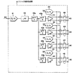
図1に示すように、この実施形態のミクスドLSIテスタは、多出力任意波形発生器10とパフォーマンス・ボード2とを備えている。パフォーマンス・ボード2は、被試験LSI(DUT)3とのインターフェイスボートとして機能する。図1では、パフォーマンス・ボード2に四つのDUT3を載置した様子を示している。 As shown in FIG. 1, the mixed LSI tester of this embodiment includes a multi-output arbitrary waveform generator 10 and a
また、多出力任意波形発生器10は、被試験LSI(DUT)3の品種固有の試験シーケンスに基づいてアナログ試験信号を生成するために、出力シーケンス制御部11と出力波形データ発生部12と、四つのポート40を有するアナログ波形生成部40と、同測対応レジスタ5とにより構成されている。
以下、各構成要素について説明する。The multi-output arbitrary waveform generator 10 includes an output sequence control unit 11, an output waveform
Hereinafter, each component will be described.
出力シーケンス制御部11は、DUT3用の試験シーケンスに基づいて、試験シーケンス信号S1を出力し、出力波形データ発生部12を制御する。
出力波形データ発生部12は、シーケンス信号S1に従って、LSI試験用の出力波形データ信号S2を生成する。そして、その出力波形データ信号S2をアナログ波形生成部4へ出力する。
また、アナログ波形生成部40は、出力波形データ発生部12より出力された出力波形データ信号S2を、デジタル/アナログ変換し、四つのDUT3にそれぞれ印加するアナログ試験信号S3を生成する。The output sequence control unit 11 outputs a test sequence signal S1 based on the test sequence for
The output
The analog
ここで、図2を参照して、アナログ波形生成部40の構成について説明する。
図2に示すように、アナログ波形生成部40は、一系統の、デジタル/アナログ変換器(D/A)41、ローパスフィルタ(LPF)42及び一段目減衰器(ATT1)43aを備えている。さらに、このアナログ波形生成部40は、四系統の、二段目減衰器(ATT2)43b、差動部44及びオフセット調整用デジタル/アナログ変換器(D/A)45を備えている。Here, the configuration of the analog
As shown in FIG. 2, the analog
そして、アナログ波形生成部40に入力された出力波形データS2は、まず、デジタル/アナログ変換器41により、デジタル/アナログ変換され、アナログ試験信号が生成される。続いて、このアナログ試験信号は、ローパスフィルタ42を通過することにより、高周波の雑音成分が除かれる。さらに、一段目減衰器43aにより、アナログ試験信号の信号振幅がおおよそDUT3の許容範囲程度となるように、3dB刻みでいったんゲイン調整される。 The output waveform data S2 input to the analog
次に、一段目減衰器43aから出力されたアナログ試験信号は、四系統に分配され、四系統の各二段目減衰器43bにそれぞれ入力される。四系統に分配された各アナログ試験信号は、それぞれ二段目減衰器43bにより、信号振幅が各DUT3の許容範囲内となるように、ゲインを個別に微調整する。各二段目減衰器43bでは、0.1dB刻みに3dBの調整幅内でゲインを個別に調整する。
続いて、ゲイン調整されたアナログ試験信号から、差動部44により、ポジ信号及びネガ信号からなる差動アナログ試験信号が生成される。Next, the analog test signal output from the first-stage attenuator 43a is distributed to four systems and input to each of the four-system second-
Subsequently, a differential analog test signal including a positive signal and a negative signal is generated by the
さらに、四系統の各差動アナログ試験信号に、各DUT3のオフセット電圧許容範囲に合わせたオフセット電圧を加算し、オフセット調整を行う。オフセット電圧と差動アナログ試験信号とは同相となっている。これらオフセット電圧は、各DUT3のオフセット電圧許容範囲に応じたDCオフセット信号S4を、オフセット調整用デジタル/アナログ変換器45でデジタル/アナログ変換して生成される。
このようにして四系統の各ポート40から、各ポートにそれぞれ接続されたDUT3ごとに最適化された、オフセット調整済みの差動アナログ試験信号が出力される。Further, an offset voltage that matches the allowable offset voltage range of each
In this way, differential analog test signals with offset adjustment optimized for each
さらに、本実施形態では、同測対応レジスタ5により、アナログ波形生成部4の出力スイッチ46の開閉がポート40別に制御される。これにより、四系統のポート40のうち、アナログ試験信号を出力するポートを任意に選択することができる。その結果、同測により試験するDUT3を選択することができる。これにより、試験プログラムを複雑化させることなく、任意のDUT3について同測により試験を行うことができる。 Furthermore, in this embodiment, the opening / closing of the
上述した実施の形態においては、本発明を特定の条件で構成した例について説明したが、本発明は、種々の変更を行うことができる。例えば、上述した実施の形態においては、パフォーマンス・ボードに四個のDUT3を載置した例について説明したが、本発明では、DUTの数は四個に限定されない。例えば、二個のDUTを同測により試験してもよいし、八個のDUTを同測により試験してもよい。 In the above-described embodiment, the example in which the present invention is configured under specific conditions has been described. However, the present invention can be variously modified. For example, in the above-described embodiment, an example in which four
また、例えば、上述の実施形態では、差動アナログ試験信号のポジ信号及びネガ信号の両方に同一のオフセット信号を加算したが、本発明では、ポジ信号とネガ信号に、互いに強度の異なるオフセット信号を別個に加算してもよい。 Further, for example, in the above-described embodiment, the same offset signal is added to both the positive signal and the negative signal of the differential analog test signal. However, in the present invention, offset signals having different intensities are added to the positive signal and the negative signal. May be added separately.
以上、詳細に説明したように、アナログ波形生成部において、アナログ試験信号を分配し、複数のポートから出力する。このため、複数の被試験LSIを同測により試験する場合であっても、出力シーケンス制御部及び出力波形データ発生部を一系統とすることができる。
その上、分配されたアナログ試験信号を、アナログ波形成生成部のゲイン調整部及びオフセット調整部により、被試験LSIごとに個別に最適化する。As described above in detail, the analog waveform generation unit distributes the analog test signal and outputs it from a plurality of ports as described in detail. Therefore, even when a plurality of LSIs under test are tested by the same measurement, the output sequence control unit and the output waveform data generation unit can be integrated into one system.
In addition, the distributed analog test signals are individually optimized for each LSI under test by the gain adjusting unit and the offset adjusting unit of the analog wave forming and generating unit.
これにより、複数個の被試験LSIを同時に試験する際に、簡単な回路構成で、被試験LSIごとに最適化されたアナログ試験信号を生成することができる。
また、本発明では、アナログ波形生成部においてアナログ試験信号を分配し、最適化しているので、パフォーマンス・ボードの回路構成を複雑化させることなく、また、試験プログラムを複雑化させることなく、デバイスごとの試験信号を最適化して同測試験を行うことができる。Thereby, when simultaneously testing a plurality of LSI under test, an analog test signal optimized for each LSI under test can be generated with a simple circuit configuration.
In the present invention, the analog waveform generation unit distributes and optimizes the analog test signal, so that the circuit configuration of the performance board is not complicated, and the test program is not complicated, for each device. The test signal can be optimized and the same measurement test can be performed.
1 任意波形発生器
2 パフォーマンス・ボード
3 被試験LSI(DUT)
4 アナログ波形生成部
10 多出力任意波形発生器
11 出力シーケンス制御部
12 出力波形データ発生部
13 アナログ波形生成部
40 ポート
41 D/A変換器
42 ローパスフィルタ
43、43a、43b 減衰器
44 差動部
45 オフセット調整用デジタル/アナログ変換器
46 出力スイッチ1
DESCRIPTION OF
Claims (2)
被試験LSI固有の試験シーケンスに基づいて、前記出力波形データ発生部を制御する出力シーケンス制御部と、
前記出力波形データ発生部より出力された出力波形データ信号を、デジタル/アナログ変換して、複数の前記被試験LSIにそれぞれ印加するアナログ試験信号を生成するアナログ波形生成部とを備えた多出力任意波形発生器であって、
前記出力シーケンス制御部及び出力波形データ発生部が一系統からなり、
前記アナログ波形生成部は、
前記出力波形データ発生部から出力される一系統の出力波形データ信号を入力して、複数の被試験LSIにそれぞれ印加される前記アナログ試験信号を個別に出力する複数のポートを有し、かつ、
前記出力波形データ発生部から出力される一系統の出力波形データ信号を入力する一系統のデジタル/アナログ変換部,フィルタ部及び一段目のゲイン調整部と、
前記一段目のゲイン調整部から出力される信号がそれぞれ入力される複数系統の、前記複数の各ポートからそれぞれ出力されるアナログ試験信号のゲインを個別に調整する複数のゲイン調整部及び前記アナログ試験信号のオフセット電圧を個別に調整する複数のオフセット調整部とを設けてあり、
全前記ポートのうち、前記アナログ試験信号を出力するポートを選択する同測対応レジスタを備える
ことを特徴とする多出力任意波形発生器。
An output waveform data generator for generating an output waveform data signal for LSI testing;
An output sequence control unit that controls the output waveform data generation unit based on a test sequence unique to the LSI under test;
An output waveform data signal output from the output waveform data generation unit is digitally / analog-converted to provide an analog waveform generation unit that generates an analog test signal to be applied to each of the plurality of LSIs to be tested. A waveform generator,
The output sequence control unit and the output waveform data generation unit consist of one system,
The analog waveform generator is
A plurality of ports for inputting an output waveform data signal of one system output from the output waveform data generator and individually outputting the analog test signals respectively applied to a plurality of LSIs under test; and
A digital / analog conversion unit, a filter unit, and a first-stage gain adjustment unit for inputting a system of output waveform data signals output from the output waveform data generation unit;
A plurality of gain adjusting units for individually adjusting the gains of the analog test signals output from the plurality of ports of the plurality of systems to which the signals output from the first-stage gain adjusting unit are respectively input, and the analog test Ri Oh provided a plurality of offset adjustment section for adjusting the offset voltage of the signal individually,
Among all the ports, multiple output arbitrary waveform generator, characterized in that Ru with a simultaneous measurement corresponding register select the port that outputs the analog test signal.
前記任意波形発生器は、
LSI試験用の出力波形データ信号を生成する出力波形データ発生部と、
被試験LSI固有の試験シーケンスに基づいて、前記出力波形データ発生部を制御する出力シーケンス制御部と、
前記出力波形データ発生部より出力された出力波形データ信号を、デジタル/アナログ変換して、複数の前記被試験LSIに印加するアナログ試験信号を生成するアナログ波形生成部とにより構成してあり、
前記出力シーケンス制御部及び出力波形データ発生部が一系統からなり、
前記アナログ波形生成部は、
前記出力波形データ発生部から出力される一系統の出力波形データ信号を入力して、複数の被試験LSIにそれぞれ印加される前記アナログ試験信号を個別に出力する複数のポートを有し、かつ、
前記出力波形データ発生部から出力される一系統の出力波形データ信号を入力する一系統のデジタル/アナログ変換部,フィルタ部及び一段目のゲイン調整部と、
前記一段目のゲイン調整部から出力される信号がそれぞれ入力される複数系統の、前記複数の各ポートからそれぞれ出力されるアナログ試験信号のゲインを個別に調整する複数のゲイン調整部及び前記アナログ試験信号のオフセット電圧を個別に調整する複数のオフセット調整部とを設けてあり、
全前記ポートのうち、前記アナログ試験信号を出力するポートを選択する同測対応レジスタを備える
ことを特徴とするミクスドLSIテスタ。 A multi-output arbitrary waveform generator for generating an analog test signal based on a test sequence specific to the type of LSI to be tested, and a performance board on which a plurality of the LSIs to be tested to which the analog test signal is applied are mounted. A mixed LSI tester provided,
The arbitrary waveform generator is
An output waveform data generator for generating an output waveform data signal for LSI testing;
An output sequence control unit that controls the output waveform data generation unit based on a test sequence unique to the LSI under test;
The output waveform data signal output from the output waveform data generation unit is configured by an analog waveform generation unit that performs digital / analog conversion and generates an analog test signal to be applied to the plurality of LSIs to be tested.
The output sequence control unit and the output waveform data generation unit consist of one system,
The analog waveform generator is
A plurality of ports for inputting an output waveform data signal of one system output from the output waveform data generator and individually outputting the analog test signals respectively applied to a plurality of LSIs under test; and
A digital / analog conversion unit, a filter unit, and a first-stage gain adjustment unit for inputting a system of output waveform data signals output from the output waveform data generation unit;
A plurality of gain adjusting units for individually adjusting the gains of the analog test signals output from the plurality of ports of the plurality of systems to which the signals output from the first-stage gain adjusting unit are respectively input, and the analog test Ri Oh provided a plurality of offset adjustment section for adjusting the offset voltage of the signal individually,
Among all the ports, Mikusudo LSI tester, characterized by Ru with a simultaneous measurement corresponding register select the port that outputs the analog test signal.
Priority Applications (4)
| Application Number | Priority Date | Filing Date | Title |
|---|---|---|---|
| JP2001004824A JP5248723B2 (en) | 2001-01-12 | 2001-01-12 | Multi-output arbitrary waveform generator and mixed LSI tester |
| PCT/JP2002/000154 WO2002056042A1 (en) | 2001-01-12 | 2002-01-11 | Multiple-output arbitrary waveform generator and mixed lsi tester |
| US10/466,455 US6768349B2 (en) | 2001-01-12 | 2002-01-11 | Multiple-output arbitrary waveform generator and mixed lsi tester |
| DE10295594T DE10295594T5 (en) | 2001-01-12 | 2002-01-11 | ARB generator with multiple outputs |
Applications Claiming Priority (1)
| Application Number | Priority Date | Filing Date | Title |
|---|---|---|---|
| JP2001004824A JP5248723B2 (en) | 2001-01-12 | 2001-01-12 | Multi-output arbitrary waveform generator and mixed LSI tester |
Publications (2)
| Publication Number | Publication Date |
|---|---|
| JP2002214292A JP2002214292A (en) | 2002-07-31 |
| JP5248723B2 true JP5248723B2 (en) | 2013-07-31 |
Family
ID=18872960
Family Applications (1)
| Application Number | Title | Priority Date | Filing Date |
|---|---|---|---|
| JP2001004824A Expired - Fee Related JP5248723B2 (en) | 2001-01-12 | 2001-01-12 | Multi-output arbitrary waveform generator and mixed LSI tester |
Country Status (4)
| Country | Link |
|---|---|
| US (1) | US6768349B2 (en) |
| JP (1) | JP5248723B2 (en) |
| DE (1) | DE10295594T5 (en) |
| WO (1) | WO2002056042A1 (en) |
Families Citing this family (20)
| Publication number | Priority date | Publication date | Assignee | Title |
|---|---|---|---|---|
| GB0222556D0 (en) * | 2002-09-28 | 2002-11-06 | Koninkl Philips Electronics Nv | RF chip testing method and system |
| KR100555544B1 (en) * | 2004-01-02 | 2006-03-03 | 삼성전자주식회사 | Apparatus for generating test stimulus signal having current source regardless of internal impedance value of a device under test |
| EP1741793B1 (en) | 2004-04-28 | 2010-08-18 | Eisai R&D Management Co., Ltd. | Method of hybridization |
| KR100548199B1 (en) * | 2004-07-15 | 2006-02-02 | 삼성전자주식회사 | Analog/Digital Mixed Signal Semiconductor Device Test apparatus |
| US7023366B1 (en) * | 2004-12-23 | 2006-04-04 | Teradyne, Inc. | Using a parametric measurement unit for converter testing |
| US20060223440A1 (en) * | 2005-04-01 | 2006-10-05 | David Stockton | Low frequency noise source and method of calibration thereof |
| US7340357B2 (en) * | 2005-05-27 | 2008-03-04 | National Instruments Corporation | Arbitrary waveform generator with configurable digital signal processing unit |
| WO2008020555A1 (en) * | 2006-08-14 | 2008-02-21 | Advantest Corporation | Test device and test method |
| US8224613B2 (en) * | 2007-03-13 | 2012-07-17 | Tektronix, Inc. | Synthesis and generation of arbitrary waveforms with ISI components for jitter tolerance |
| JP4928339B2 (en) * | 2007-04-26 | 2012-05-09 | 株式会社アドバンテスト | Arbitrary waveform generator |
| JP2008107366A (en) * | 2008-01-09 | 2008-05-08 | Renesas Technology Corp | Interface circuit |
| KR101138199B1 (en) * | 2008-06-02 | 2012-05-10 | 가부시키가이샤 어드밴티스트 | Test wafer unit and test system |
| JP4803227B2 (en) * | 2008-09-03 | 2011-10-26 | 横河電機株式会社 | Test signal generator |
| JP4565036B2 (en) | 2009-01-05 | 2010-10-20 | ファナック株式会社 | Motor insulation deterioration detector |
| JP2009180749A (en) * | 2009-05-21 | 2009-08-13 | Advantest Corp | Noise generator, measurement apparatus, and testing apparatus |
| US8572143B2 (en) * | 2009-11-09 | 2013-10-29 | Agilent Technologies, Inc. | Waveform generator with a register that shifts and provides groups of successive data values from an input data stream |
| JP5547514B2 (en) * | 2010-02-15 | 2014-07-16 | 株式会社アドバンテスト | Signal generator and test apparatus using the same |
| JP5761976B2 (en) * | 2010-12-08 | 2015-08-12 | 株式会社アドバンテスト | Semiconductor device, test apparatus, and manufacturing method |
| JP5680987B2 (en) * | 2011-02-18 | 2015-03-04 | 株式会社アドバンテスト | Semiconductor device, test apparatus, and manufacturing method |
| CN104698234A (en) * | 2015-03-09 | 2015-06-10 | 哈尔滨工程大学 | Portable double-amplitude shifted signal generator |
Family Cites Families (6)
| Publication number | Priority date | Publication date | Assignee | Title |
|---|---|---|---|---|
| JPH0964745A (en) * | 1995-08-21 | 1997-03-07 | Advantest Corp | Optional waveform generator |
| JPH10123213A (en) * | 1996-10-18 | 1998-05-15 | Nec Corp | Semiconductor integrated circuit |
| JP3827821B2 (en) * | 1997-07-22 | 2006-09-27 | 株式会社アドバンテスト | Semiconductor test equipment |
| US5951705A (en) * | 1997-10-31 | 1999-09-14 | Credence Systems Corporation | Integrated circuit tester having pattern generator controlled data bus |
| JPH11337616A (en) * | 1998-05-22 | 1999-12-10 | Mitsumi Electric Co Ltd | Circuit measuring instrument |
| JP4105831B2 (en) * | 1998-09-11 | 2008-06-25 | 株式会社アドバンテスト | Waveform generator, semiconductor test apparatus, and semiconductor device |
-
2001
- 2001-01-12 JP JP2001004824A patent/JP5248723B2/en not_active Expired - Fee Related
-
2002
- 2002-01-11 WO PCT/JP2002/000154 patent/WO2002056042A1/en active Application Filing
- 2002-01-11 US US10/466,455 patent/US6768349B2/en not_active Expired - Lifetime
- 2002-01-11 DE DE10295594T patent/DE10295594T5/en not_active Withdrawn
Also Published As
| Publication number | Publication date |
|---|---|
| DE10295594T5 (en) | 2004-04-29 |
| US20040070410A1 (en) | 2004-04-15 |
| US6768349B2 (en) | 2004-07-27 |
| JP2002214292A (en) | 2002-07-31 |
| WO2002056042A1 (en) | 2002-07-18 |
Similar Documents
| Publication | Publication Date | Title |
|---|---|---|
| JP5248723B2 (en) | Multi-output arbitrary waveform generator and mixed LSI tester | |
| KR100421277B1 (en) | Architecture for rf signal automatic test equipment | |
| EP1149474A1 (en) | Calibration and compensation of delta sigma adc's and dac's by correlating noise signals | |
| US6737881B2 (en) | Apparatus for testing integrated circuits having an integrated unit for testing digital and analog signals | |
| KR20030045939A (en) | Test apparatus for semiconductor integraged circuit | |
| US6374379B1 (en) | Low-cost configuration for monitoring and controlling parametric measurement units in automatic test equipment | |
| US5644505A (en) | Universal audio analyzer | |
| US6768390B1 (en) | System and method for generating balanced modulated signals with arbitrary amplitude and phase control using modulation | |
| US6285744B1 (en) | Telephony test system with adjustable output impedance | |
| US5918198A (en) | Generating pulses in analog channel of ATE tester | |
| JP2009180749A (en) | Noise generator, measurement apparatus, and testing apparatus | |
| JP4392342B2 (en) | Parallel source / capture architecture | |
| JP4493145B2 (en) | Arbitrary waveform generator | |
| JP2001183431A (en) | Testing device and testing method | |
| JP3697400B2 (en) | Signal generator | |
| WO2006129491A1 (en) | Jitter generating circuit | |
| JP2624920B2 (en) | Vertical amplifier calibration system for multi-phenomenon oscilloscope | |
| JP2002372571A (en) | Semiconductor test device | |
| JP3827821B2 (en) | Semiconductor test equipment | |
| KR100340057B1 (en) | Testing method of analog to digital conveter | |
| JP2962213B2 (en) | Test circuit and test method for semiconductor integrated circuit | |
| JP3053228B2 (en) | Semiconductor test equipment | |
| JP2008278031A (en) | Differential output device and arbitrary waveform generating device | |
| JPH04259868A (en) | Ic tester | |
| JP2004108840A (en) | Semiconductor testing apparatus |
Legal Events
| Date | Code | Title | Description |
|---|---|---|---|
| A621 | Written request for application examination |
Free format text: JAPANESE INTERMEDIATE CODE: A621 Effective date: 20071214 |
|
| A131 | Notification of reasons for refusal |
Free format text: JAPANESE INTERMEDIATE CODE: A131 Effective date: 20110201 |
|
| A521 | Request for written amendment filed |
Free format text: JAPANESE INTERMEDIATE CODE: A523 Effective date: 20110404 |
|
| A131 | Notification of reasons for refusal |
Free format text: JAPANESE INTERMEDIATE CODE: A131 Effective date: 20120228 |
|
| A521 | Request for written amendment filed |
Free format text: JAPANESE INTERMEDIATE CODE: A523 Effective date: 20120419 |
|
| TRDD | Decision of grant or rejection written | ||
| A01 | Written decision to grant a patent or to grant a registration (utility model) |
Free format text: JAPANESE INTERMEDIATE CODE: A01 Effective date: 20130402 |
|
| A61 | First payment of annual fees (during grant procedure) |
Free format text: JAPANESE INTERMEDIATE CODE: A61 Effective date: 20130411 |
|
| R150 | Certificate of patent or registration of utility model |
Free format text: JAPANESE INTERMEDIATE CODE: R150 |
|
| FPAY | Renewal fee payment (event date is renewal date of database) |
Free format text: PAYMENT UNTIL: 20160419 Year of fee payment: 3 |
|
| LAPS | Cancellation because of no payment of annual fees |