JP5242614B2 - Chip resistor and manufacturing method thereof - Google Patents
Chip resistor and manufacturing method thereof Download PDFInfo
- Publication number
- JP5242614B2 JP5242614B2 JP2010058657A JP2010058657A JP5242614B2 JP 5242614 B2 JP5242614 B2 JP 5242614B2 JP 2010058657 A JP2010058657 A JP 2010058657A JP 2010058657 A JP2010058657 A JP 2010058657A JP 5242614 B2 JP5242614 B2 JP 5242614B2
- Authority
- JP
- Japan
- Prior art keywords
- resistor
- electrodes
- pair
- insulating layer
- edge
- Prior art date
- Legal status (The legal status is an assumption and is not a legal conclusion. Google has not performed a legal analysis and makes no representation as to the accuracy of the status listed.)
- Expired - Lifetime
Links
Images


Description
本願発明は、チップ抵抗器およびその製造方法に関する。 The present invention relates to a chip resistor and a manufacturing method thereof.
従来のチップ抵抗器の一例としては、図12に示すようなものがある(特許文献1参照)。図示されたチップ抵抗器Bは、金属製のチップ状の抵抗体90の下面90bに、一対の電極91が空隙部93を介して離間して設けられた構成を有している。各電極91の下面には、実装時のハンダ付け性を良くするための手段として、ハンダ層92が形成されている。
An example of a conventional chip resistor is shown in FIG. 12 (see Patent Document 1). The illustrated chip resistor B has a configuration in which a pair of
このチップ抵抗器Bは、図13に示すような方法により製造される。まず、同図(a)に示すように、抵抗体90および電極91のそれぞれの材料として、2枚の金属板90’, 91’を準備し、同図(b)に示すように、金属板90’の下面に金属板91’を重ね合わせて接合する。次いで、同図(c)に示すように、金属板91’の一部を機械加工によって切削し、空隙部93を形成する。その後は、同図(d)に示すように、金属板91’の下面にハンダ層92’を形成してから、同図(e)に示すように、金属板90’, 91’を切断する。このことにより、チップ抵抗器Bが製造される。
This chip resistor B is manufactured by a method as shown in FIG. First, as shown in FIG. 5A, two
上記したチップ抵抗器Bは、抵抗体90の下面90bのうち、一対の電極91間の領域や、抵抗体90の各側面90cは絶縁保護されていない構造となっている。このため、ハンダを利用してチップ抵抗器Bを所望箇所に面実装するときには、各電極91の下方からはみ出したハンダの一部が、抵抗体90の下面90bや各側面90cに付着する場合があった。このような事態が生じたのでは、抵抗値に大きな誤差が生じ、チップ抵抗器Bを利用して構成される電気回路の仕様に狂いを生じてしまう。このような不具合は、チップ抵抗器Bの低抵抗化が図られて、抵抗値の誤差を少なくする必要性が高くなるほどより深刻となる。
The chip resistor B described above has a structure in which the region between the pair of
また、上記従来技術においては、チップ抵抗器Bの製造作業が煩雑であり、その生産性が悪いという不具合もあった。より具体的には、従来においては、空隙部93の形成は、機械加工により行なっている。また、その加工は、一対の電極91間の寸法s5を精度良く仕上げなければならない。このため、上記加工はかなり慎重に行なう必要があり、チップ抵抗器Bの生産性が悪くなっていた。さらに、上記従来技術においては、切削加工を経てチップ抵抗器Bが製造されるために、その切削加工精度に起因する電極間抵抗値の誤差も発生していた。
Moreover, in the said prior art, there existed a malfunction that the manufacture operation | work of the chip resistor B was complicated and the productivity was bad. More specifically, conventionally, the
本願発明は、上記した事情のもとで考え出されたものであって、抵抗体へのハンダ付着に起因して抵抗値に誤差が発生するといった不具合を解消し、または抑制することが可能なチップ抵抗器を提供することをその課題としている。また、本願発明は、そのようなチップ抵抗器を効率良く、かつ適切に製造することが可能なチップ抵抗器の製造方法を提供することを他の課題としている。 The present invention has been conceived under the circumstances described above, and it is possible to eliminate or suppress such a problem that an error occurs in the resistance value due to solder adhesion to the resistor. The problem is to provide a chip resistor. Moreover, this invention makes it the other subject to provide the manufacturing method of the chip resistor which can manufacture such a chip resistor efficiently and appropriately.
上記の課題を解決するため、本願発明では、次の技術的手段を講じている。 In order to solve the above problems, the present invention takes the following technical means.
本願発明の第1の側面によって提供されるチップ抵抗器は、厚み方向に間隔を隔てた表裏面および幅方向に間隔を隔てて一定方向に延びた一対の側面を有するチップ状の金属製抵抗体と、上記抵抗体の裏面に上記一定方向において間隔を隔てて並ぶように設けられた一対の電極と、を備えているチップ抵抗器であって、上記抵抗体の裏面のうち、上記一対の電極間の領域を全て覆い、上記一対の電極の形成前に形成されることにより上記一対の電極の形成領域を規定して上記一対の電極間抵抗値を決定する第1の絶縁層と、上記抵抗体の上記一対の側面をそれぞれ全て覆う第2の絶縁層と、を備えており、上記一対の電極は、メッキにより上記抵抗体の全幅にわたって形成されているとともに、当該一対の電極には、その表面の全面を覆うようにメッキにより形成されたハンダ層が積層されており、かつ、上記一対の電極の端縁および上記ハンダ層の端縁は、上記第1の絶縁層に直接接触するように当該第1の絶縁層の縁部上にオーバラップしていることを特徴とする。 The chip resistor provided by the first aspect of the present invention is a chip-shaped metal resistor having front and back surfaces spaced apart in the thickness direction and a pair of side surfaces extending in a certain direction spaced apart in the width direction. And a pair of electrodes provided on the back surface of the resistor so as to be arranged at intervals in the fixed direction, wherein the pair of electrodes out of the back surface of the resistor A first insulating layer that covers all of the region between the electrodes and that is formed before the pair of electrodes is formed, thereby defining a region where the pair of electrodes is formed and determining a resistance value between the pair of electrodes; and the resistor a second insulating layer covering all the body of the pair of side surfaces, respectively, provided with said pair of electrodes, together are formed over the entire width of the resistor by plating on the pair of electrodes, the I'll cover the whole surface And a solder layer formed by plating is laminated, and the edge of the edge and the solder layer of said pair of electrodes, said first insulating layer in direct contact with said first insulating layer It is characterized by overlapping on the edge of the.
好ましい実施の形態では、上記第2の絶縁層は、上記一対の電極と上記ハンダ層の形成前に形成されることにより、上記一対の電極は、その一部が上記第2の絶縁層の端縁にオーバラップしている。 In a preferred embodiment, the second insulating layer is formed before the pair of electrodes and the solder layer are formed, so that a part of the pair of electrodes is an end of the second insulating layer. It overlaps the edge.
好ましい実施の形態では、上記抵抗体の表面を全て覆う第3の絶縁層をさらに備えている。 In a preferred embodiment, a third insulating layer that covers the entire surface of the resistor is further provided.
好ましい実施の形態では、上記各電極の厚みは、上記第1の絶縁層の厚みよりも大きくされている。 In a preferred embodiment, the thickness of each electrode is larger than the thickness of the first insulating layer.
本願発明の第2の側面によって提供されるチップ抵抗器の製造方法は、厚み方向に間隔を隔てた表裏面および幅方向に間隔を隔てて一定方向に延びた一対の側面を有するチップ状の金属製抵抗体と、上記抵抗体の裏面に上記一定方向において間隔を隔てて並ぶように設けられた一対の電極と、上記抵抗体の裏面のうち、上記一対の電極間の領域を全て覆い、上記一対の電極の形成前に形成されることにより上記一対の電極の形成領域を規定して上記一対の電極間抵抗値を決定する第1の絶縁層と、上記抵抗体の上記一対の側面をそれぞれ全て覆う第2の絶縁層と、を備えており、上記一対の電極は、メッキにより上記抵抗体の全幅にわたって形成されているとともに、当該一対の電極には、その表面の全面を覆うようにメッキにより形成されたハンダ層が積層されており、かつ、上記一対の電極の端縁および上記ハンダ層の端縁は、上記第1の絶縁層に直接接触するように当該第1の絶縁層の縁部上にオーバラップしているチップ抵抗器の製造方法であって、それ自体がバー状の抵抗体材料の裏面にこの抵抗体材料の長手方向に間隔を隔てて並んだ複数の電極と、上記複数の電極に積層されたハンダ層と、上記抵抗体材料の上記裏面の上記複数の電極間領域を全て覆い、上記電極の形成前に形成されることにより上記電極の形成領域を規定する第1の絶縁層と、上記抵抗体材料の一対の側面の全てを覆う第2の絶縁層とが形成され、上記複数の電極と上記ハンダ層とはそれらの端縁が上記第1の絶縁層に直接接触するように当該第1の絶縁層の縁部上にオーバラップしている、バー状の抵抗器集合体を作製する工程と、上記抵抗器集合体をその長手方向の複数箇所において切断することにより、複数の上記チップ抵抗器に分割する工程と、を有していることを特徴とする。 The chip resistor manufacturing method provided by the second aspect of the present invention is a chip-like metal having front and back surfaces spaced apart in the thickness direction and a pair of side surfaces extending in a constant direction spaced apart in the width direction. and manufacturing the resistor, and a pair of electrodes provided so as to be arranged at intervals in the predetermined direction on the rear surface of the resistor, of the back surface of the upper Symbol resistor, it covers all regions between the pair of electrodes, A first insulating layer that defines a formation region of the pair of electrodes to determine a resistance value between the pair of electrodes by being formed before the pair of electrodes is formed; and the pair of side surfaces of the resistor. Each of the pair of electrodes is formed over the entire width of the resistor by plating and covers the entire surface of the pair of electrodes. Formed by plating Solder layer is laminated, and the edge and the edge of the solder layer of the pair of electrodes, over to the first of the in direct contact with the insulating layer the first insulating layer edge on A method of manufacturing a wrapping chip resistor, comprising a plurality of electrodes arranged on the back surface of a bar-shaped resistor material at intervals in the longitudinal direction of the resistor material, and the plurality of electrodes. A laminated solder layer, and a first insulating layer that covers all of the plurality of inter-electrode regions on the back surface of the resistor material and defines the electrode forming region by being formed before forming the electrode; A second insulating layer covering all of the pair of side surfaces of the resistor material is formed, and the plurality of electrodes and the solder layer have their edges in direct contact with the first insulating layer. have any overlap on the edge of the first insulating layer, bar And a step of dividing the resistor assembly into a plurality of the chip resistors by cutting the resistor assembly at a plurality of positions in the longitudinal direction. To do.
好ましい実施の形態では、上記バー状の抵抗器集合体を作製する工程は、抵抗体材料としてのプレートの片面にパターン形成された絶縁層と、上記各電極となり、一部が上記絶縁層の縁部に直接接触してオーバラップするようにメッキにより形成した導電層と、上記導体層上に端縁が上記絶縁層の縁部に直接接触してオーバラップするようにメッキにより形成したハンダ層とを順次設けた後に、上記プレートを上記バー状の抵抗体材料に分割する工程と、上記バー状の抵抗体材料の一対の側面に絶縁層を形成する工程と、を含んでいる。 In a preferred embodiment, the step of producing the bar-shaped resistor assembly includes an insulating layer patterned on one side of a plate as a resistor material and the electrodes, and a part of the edge of the insulating layer. a conductive layer formed by plating so as to overlap in direct contact with the parts, and a solder layer formed by plating such edge in the conductor layer can overlap in direct contact with the edge of the insulating layer Are sequentially provided, and a step of dividing the plate into the bar-shaped resistor material and a step of forming an insulating layer on a pair of side surfaces of the bar-shaped resistor material are included.
本願発明の第3の側面によって提供されるチップ抵抗器の製造方法は、厚み方向に間隔を隔てた表裏面および幅方向に間隔を隔てて一定方向に延びた一対の側面を有するチップ状の金属製抵抗体と、上記抵抗体の裏面に上記一定方向において間隔を隔てて並ぶように設けられた一対の電極と、上記抵抗体の裏面のうち、上記一対の電極間の領域を全て覆い、上記一対の電極の形成前に形成されることにより上記一対の電極の形成領域を規定して上記一対の電極間抵抗値を決定する第1の絶縁層と、上記抵抗体の上記一対の側面をそれぞれ全て覆う第2の絶縁層と、を備えており、上記一対の電極は、メッキにより上記抵抗体の全幅にわたって形成されているとともに、当該一対の電極には、その表面の全面を覆うようにメッキにより形成されたハンダ層が積層されており、かつ、上記一対の電極の端縁および上記ハンダ層の端縁は、上記第1の絶縁層に直接接触するように当該第1の絶縁層の縁部上にオーバラップしているとともに、上記第2の絶縁層は上記一対の電極と上記ハンダ層の形成前に形成されることにより、上記一対の電極は、その一部が上記第2の絶縁層の端縁上にオーバラップしているチップ抵抗器の製造方法であって、それ自体がバー状の抵抗体材料の裏面にこの抵抗体材料の長手方向に間隔を隔てて並んだ複数の電極と、上記複数の電極に積層されたハンダ層と、上記抵抗体材料の上記裏面の上記複数の電極間領域を全て覆い、上記電極の形成前に形成されることにより上記電極の形成領域を規定する第1の絶縁層と、上記抵抗体材料の一対の側面の全てを覆う第2の絶縁層とが形成され、上記複数の電極と上記ハンダ層とはそれらの端縁が上記第1の絶縁層に直接接触するように当該第1の絶縁層の縁部上にオーバラップしている、バー状の抵抗器集合体を作製する工程と、上記抵抗器集合体をその長手方向の複数箇所において切断することにより、複数の上記チップ抵抗器に分割する工程と、を有しており、上記バー状の抵抗器集合体を作製する工程は、抵抗体材料としてのプレートの片面に上記第1絶縁層のための絶縁層をパターン形成した後に、上記プレートを上記バー状の抵抗体材料に分割する工程と、上記バー状の抵抗体材料の一対の側面に上記第2絶縁層を形成する工程と、上記パターン形成された絶縁層が形成されている面に、複数の電極をその端縁が上記パターン形成された絶縁層の縁部と、上記第2絶縁層の端縁とに直接接触してオーバラップするようにメッキにより形成する工程と、上記複数の電極上に上記ハンダ層をその端縁が上記パターン形成された絶縁層の縁部に直接オーバラップするようにメッキにより形成する工程と、を含んでいることを特徴とする。 The chip resistor manufacturing method provided by the third aspect of the present invention comprises a chip-like metal having front and back surfaces spaced apart in the thickness direction and a pair of side surfaces extending in a constant direction spaced apart in the width direction. and manufacturing the resistor, and a pair of electrodes provided so as to be arranged at intervals in the predetermined direction on the rear surface of the resistor, of the back surface of the upper Symbol resistor, it covers all regions between the pair of electrodes, A first insulating layer that defines a formation region of the pair of electrodes to determine a resistance value between the pair of electrodes by being formed before the pair of electrodes is formed; and the pair of side surfaces of the resistor. Each of the pair of electrodes is formed over the entire width of the resistor by plating and covers the entire surface of the pair of electrodes. Formed by plating Solder layer is laminated, and the edge and the edge of the solder layer of the pair of electrodes, over to the first of the in direct contact with the insulating layer the first insulating layer edge on The second insulating layer is wrapped and formed before the pair of electrodes and the solder layer are formed, so that a part of the pair of electrodes is an edge of the second insulating layer. A method of manufacturing an overlying chip resistor, comprising a plurality of electrodes arranged on the back surface of a resistor material of a bar shape at intervals in the longitudinal direction of the resistor material, A solder layer laminated on the electrode and a plurality of inter-electrode regions on the back surface of the resistor material, and are formed before the electrode is formed, thereby defining a formation region of the electrode. Cover all of the insulating layer and the pair of side surfaces of the resistor material. A second insulating layer is formed, overlapped on the first insulating layer edge on to the said plurality of electrode and the solder layer their edges in direct contact with the first insulating layer Forming a bar-shaped resistor assembly, and dividing the resistor assembly into a plurality of chip resistors by cutting the resistor assembly at a plurality of locations in the longitudinal direction. The bar-shaped resistor assembly is formed by patterning an insulating layer for the first insulating layer on one side of a plate as a resistor material, and then the plate-shaped resistor assembly. a step of dividing the body material, and forming the second insulating layer on the pair of side surfaces of the bar-like resistor material, the surface of the patterned insulation layer is formed, a plurality of electrodes Insulating layer whose edge is patterned as above And the edge of a step of forming by plating so as to overlap in direct contact with the edge of the second insulating layer, the solder layer on the plurality of electrodes that edge is the patterned And a step of forming by plating so as to directly overlap the edge of the insulating layer.
本願発明のその他の特徴および利点については、以下に行う発明の実施の形態の説明から、より明らかになるであろう。 Other features and advantages of the present invention will become more apparent from the following description of embodiments of the invention.
以下、本願発明の好ましい実施の形態について、図面を参照しつつ具体的に説明する。 Hereinafter, a preferred embodiment of the present invention will be specifically described with reference to the drawings.
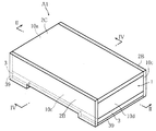
図1〜図4は、本願発明に係るチップ抵抗器の一例を示している。図1および図2によく表われているように、本実施形態のチップ抵抗器A1は、抵抗体1、第1ないし第3の絶縁層2A〜2C、および一対の電極3を具備している。
1 to 4 show an example of a chip resistor according to the present invention. As clearly shown in FIGS. 1 and 2, the chip resistor A <b> 1 of this embodiment includes a
抵抗体1は、各部の厚みが一定の矩形チップ状であり、金属製である。その具体的な材質としては、Ni−Cu系合金、Cu−Mn系合金、Ni−Cr系合金などが挙げられるが、これらに限定されるものではなく、チップ抵抗器A1のサイズと目標抵抗値に見合った抵抗率をもつものを適宜選択すればよい。現実的ではないが、抵抗体1を非金属製とすることも可能である。
The
第1ないし第3の絶縁層2A〜2Cは、いずれもエポキシ樹脂系などの樹脂膜である。第1の絶縁層2Aは、抵抗体1の裏面10bのうち、一対の電極3間の領域の全体を覆うように設けられている。第2の絶縁層2Bは、図4によく表われているように、抵抗体1の一対の側面10cのそれぞれの全体を覆うように設けられている。第3の絶縁層2Cは、抵抗体1の表面10aの全体を覆うように設けられている。抵抗体1は、その両端面10dのみが非被覆状態の露出面となっている。
The first to third insulating
一対の電極3は、抵抗体1の裏面10bに設けられており、第1の絶縁層2Aを挟むようにして一対の側面10cが延びる方向に離間している。これら一対の電極3は、後述するように、たとえば抵抗体1に銅メッキを施すことにより形成されたものである。各電極3は、第1の絶縁層2Aの幅方向の端面20との間に隙間が生じないように端面20に接している。このことにより、一対の電極3の間隔は、第1の絶縁層2Aによって規定されており、第1の絶縁層2Aの幅s1と同一の寸法となっている。各電極3の下面には、ハンダ付け性を良好にするためのハンダ層39が積層して形成されている。
The pair of
図1および図2においては、電極3やハンダ層39の端部を概略的に示しているが、これら電極3やハンダ層39はメッキにより形成されているために、実際には、図3の符号n1で示すように、それらの一部分は第1の絶縁層2A上にオーバラップしている。ただし、このオーバラップしている部分自体は、抵抗体1の裏面10bに直接接触している訳ではないため、抵抗体1の電極間抵抗値に誤差を生じさせる要因にはならない。各電極3の厚みt1は、第1の絶縁層2Aの厚みt2よりも大きくされており、各電極3およびハンダ層39は、第1の絶縁層2Aの下面よりも下方に突出した構造となっている。
1 and 2 schematically show the end portions of the
上記各部の厚みの一例を挙げると、第1ないし第3の絶縁層2A〜2Cがそれぞれ20μm程度、各電極3が30μm程度、各ハンダ層39が5μm程度である。抵抗体1については、その厚みが0.1mm〜1mm程度、縦および横の寸法はそれぞれ2mm〜7mm程度である。ただし、この抵抗体1のサイズについては、目標抵抗値の大きさに応じて種々に変更されることは言うまでもない。また、このチップ抵抗器A1は、0.5mΩ〜100mΩ程度の低抵抗のものとして構成されている。チップ抵抗器A1の電極間抵抗は、抵抗体1の抵抗率、電極3間の距離、および抵抗体1の厚みにより決定される。
As an example of the thickness of each part, the first to third insulating
次に、上記したチップ抵抗器A1の製造方法の一例について、図5〜図7を参照して説明する。 Next, an example of a manufacturing method of the above-described chip resistor A1 will be described with reference to FIGS.
まず、図5(a)に示すように、抵抗体1の材料となる金属製のプレート1Aを準備する。このプレート1Aは、抵抗体1を複数個取り可能な縦横のサイズを有するものであり、全体にわたって厚みの均一化が図られたものである。同図(b)に示すように、このプレート1Aの上向きの片面10aの全体または略全体には、第3の絶縁層2C'を形成する。この第3の絶縁層2C'の形成は、たとえばエポキシ樹脂をベタ塗り状に厚膜印刷して行なう。この第3の絶縁層2C'の表面に標印を施す工程を行なってもよい。
First, as shown in FIG. 5A, a
次いで、同図(c)に示すように、プレート1Aを表裏反転させてから、プレート1Aの上向きとなった面10bに、複数の第1の絶縁層2A'をストライプ状に並べるようにして形成する。これら第1の絶縁層2A'の形成は、第3の絶縁層2C'の形成に用いたのと同一の樹脂および装置を用いて厚膜印刷により行なう。このようにすれば、複数種類の材料や装置を用いる場合と比較すると、チップ抵抗器A1の製造コストを削減するのに好ましい。上記厚膜印刷の手法によれば、各第1の絶縁層2A'の幅などを所定の寸法に正確に仕上げることができる。
Next, as shown in FIG. 6C, after the
プレート1Aの面10bのうち、複数の第1の絶縁層2A'どうしの間の領域には、図6(d)に示すように、導電層3A'とハンダ層39A'とを形成する。導電層3A'は電極3の原型となる部分であり、その形成はたとえば銅メッキにより行なう。メッキ処理によれば、導電層3A'と第1の絶縁層2A'との間に隙間を生じさせないようにして、隣り合う第1の絶縁層2A'間の領域に導電層3A'を均一に形成することが可能である。ハンダ層39A'の形成もたとえばメッキ処理によって行なう。
As shown in FIG. 6D, a
その後は、図6(e)に示すように、プレート1Aを各導電層3A'や各第1の絶縁層2A'が延びる方向とは直交する方向において切断し、複数のバー状の抵抗体材料1A'に分割する。次いで、図7(f)に示すように、このバー状の抵抗体材料1A'の一対の側面10cのそれぞれに第2の絶縁層2B'を形成する。これにより、チップ抵抗器A1が直列に繋がった構成に相当するバー状の抵抗器集合体A1'が得られる。なお、第2の絶縁層2B'は、導電層3A'やハンダ層39A'の側面を覆うこととなるが、これはチップ抵抗器の機能や品質に悪影響を及ぼすものではない。
Thereafter, as shown in FIG. 6 (e), the
抵抗器集合体A1'を製造した後には、同図(g)に示すように、これを切断して複数のチップに分割していく。この作業は、たとえば各導電層3A'を抵抗器集合体A1'の長手方向において分断するように、同図仮想線C1で示す箇所を切断することにより行なう。これにより、各導電層3A'は、チップ抵抗器A1の電極3となり、1つの抵抗器集合体A1'から複数のチップ抵抗A1が好適に製造される。
After the resistor assembly A1 ′ is manufactured, it is cut and divided into a plurality of chips as shown in FIG. This operation is performed, for example, by cutting a portion indicated by a virtual line C1 in the figure so as to divide each
次に、チップ抵抗器A1の作用について説明する。 Next, the operation of the chip resistor A1 will be described.
まず、このチップ抵抗器A1は、所望の実装対象領域に対し、たとえばハンダリフローの手法を用いて面実装される。このハンダリフローの手法では、実装対象領域に設けられている端子上にクリームハンダを塗布してから、その上に各電極3を接触させるようにチップ抵抗器A1を載置した状態で、リフロー炉を利用して加熱する。各電極3は、第1の絶縁層2Aの下面よりも下方に突出しているために、各電極3の下面へのハンダ付着の確実化が図られる。
First, the chip resistor A1 is surface-mounted on a desired mounting target area by using, for example, a solder reflow technique. In this solder reflow technique, cream solder is applied to the terminals provided in the mounting target area, and then the chip resistor A1 is placed so that each
上記面実装時には、溶融ハンダが上記端子からはみ出す場合がある。ところが、抵抗体1の裏面10bの電極3間の領域と抵抗体1の各側面10cとは、第1および第2の絶縁層2A,2Bにより覆われているために、抵抗体1のそれらの面にハンダが直接付着することはない。したがって、抵抗体1に対する不当なハンダ付着に起因して抵抗値誤差が発生することはない。また、抵抗体1の表面10aは第3の絶縁層2Cによって覆われているために、この表面10aと他の部材や機器との間に不当な電気導通が生じることも防止される。なお、抵抗体1の一対の端面10dは露出しているために、この端面10dに対してはハンダを付着させることによりハンダフィレットを形成し、ハンダ接合強度を高めることが可能である。
At the time of the surface mounting, the molten solder may protrude from the terminal. However, since the region between the
このチップ抵抗器A1の抵抗体1は、プレート1Aを切断することにより形成されるが、そのサイズについては高い寸法精度に仕上げることが可能である。抵抗体1の厚みについては、プレート1Aの段階から正確に仕上げることができる。また、一対の電極3間の寸法s1は、第1の絶縁層2Aの幅と一致するが、この第1の絶縁層2Aは厚膜印刷によってかなり高い寸法精度で形成することが可能であるから、上記寸法s1も高い精度で所望の寸法に仕上げることができる。このように、抵抗体1のサイズおよび一対の電極3間の寸法s1が高い精度に仕上げられていれば、このチップ抵抗器A1の電極間抵抗値の誤差を非常に小さくすることが可能である。したがって、このチップ抵抗器A1においては、その製造後に、抵抗値調整を行なうためのトリミングを行なう必要を無くすことができる。トリミングを無くすことができれば、その分だけチップ抵抗器A1のコストを下げることができる。
The
また、本実施形態のチップ抵抗器A1の製造に際しては、従来技術とは異なり、金属板の一部に切削加工を施すことによって一対の電極を形成するといった必要はないため、製造作業の効率も良い。したがって、チップ抵抗器A1のコストをより低減することが可能である。 Further, unlike the prior art, when manufacturing the chip resistor A1 of the present embodiment, it is not necessary to form a pair of electrodes by cutting a part of a metal plate. good. Therefore, the cost of the chip resistor A1 can be further reduced.
図8〜図11は、本願発明の他の実施形態を示している。これらの図において、上記実施形態と同一または類似の要素には、同一の符号を付している。 8 to 11 show another embodiment of the present invention. In these drawings, elements that are the same as or similar to those in the above embodiment are given the same reference numerals.
図8に示すチップ抵抗器A2は、第2の絶縁層2Bが各電極3やハンダ層39の側面を覆っていない点において上記したチップ抵抗器A1とは相違しており、それ以外の構成はチップ抵抗器A1と同様である。
The chip resistor A2 shown in FIG. 8 is different from the above-described chip resistor A1 in that the second insulating
このチップ抵抗器A2は、たとえば図9に示すような工程により製造される。すなわち、同図(a)に示すように、まずプレート1Aの片面上に第1の絶縁層2A'をストライプ状に形成するとともに、その反対面に第3の絶縁層2C'を形成してから、プレート1Aをバー状の抵抗体材料1A'として切断する。その後は、同図(b)に示すように、この抵抗体材料1A'の一対の側面に第2の絶縁層2B'を形成する。また、同図(c)に示すように、第1の絶縁層2A'どうしの間の領域に、導電層3A'およびハンダ層39A'を形成する。これにより、バー状の抵抗器集合体A2'が得られる。その後は、同図(d)に示すように、抵抗器集合体A2'を複数のチップに切断する。この切断作業により、図8に示したチップ抵抗器A2が得られる。このチップ抵抗器A2においても、チップ抵抗器A1について述べたのと同様な作用が得られる。
This chip resistor A2 is manufactured by a process as shown in FIG. 9, for example. That is, as shown in FIG. 2A, first, the first insulating
図10は、製造方法の他の例を示している。この製造方法においては、先ず同図(a)に示すように、バー状の抵抗体材料1A'を準備しておく。次いで、同図(b)に示すように、この抵抗体材料1A'に第1ないし第3の絶縁層2A'〜2C'、複数の導電層3A'およびハンダ層39A'を形成することにより、抵抗器集合体A2'を作製する。その後は、同図(c)に示すように、抵抗器集合体A2'を切断して複数のチップ抵抗器A2に分割する。このように 本願発明においては、抵抗器集合体の作製に際しては、プレート状の抵抗体材料を用いるのに代えて、当初からバー状の抵抗体材料を用いてもかまわない。
FIG. 10 shows another example of the manufacturing method. In this manufacturing method, first, a bar-shaped
また、本願発明においては、バー状の抵抗器集合体としては、たとえばチップ状に切断することによって直ちに本願発明が意図するチップ抵抗器が得られる構成とされていなくてもかまわない。たとえば、バー状の抵抗器集合体としては、バー状の抵抗体材料の裏面にその長手方向に間隔を隔てて並んだ複数の電極とこれら複数の電極間領域を覆う第1の絶縁層とが設けられたものとして製作してもかまわない。この場合には、上記抵抗器集合体をその長手方向の複数箇所において切断することにより、抵抗体の側面が露出した複数のチップ抵抗器に分割した後に、それら複数のチップ抵抗器の各抵抗体の側面に個別に塗装を施すなどして第2の絶縁層を形成してもかまわない。このような方法によっても、本
願発明が意図するチップ抵抗器を製造することができる。
In the present invention, the bar-shaped resistor assembly may not have a configuration in which the chip resistor intended by the present invention is obtained immediately by cutting into a chip shape, for example. For example, a bar-shaped resistor assembly includes a plurality of electrodes arranged at intervals in the longitudinal direction on the back surface of a bar-shaped resistor material, and a first insulating layer covering the plurality of inter-electrode regions. It may be produced as provided. In this case, the resistor assembly is divided into a plurality of chip resistors whose side surfaces are exposed by cutting the resistor assembly at a plurality of positions in the longitudinal direction, and then each resistor of the plurality of chip resistors is divided. Alternatively, the second insulating layer may be formed by individually coating the side surfaces. Also by such a method, the chip resistor intended by the present invention can be manufactured.
むろん、本願発明に係るチップ抵抗器は、本願発明に係るチップ抵抗器の製造方法とは異なる製造方法により製造することも可能である。たとえば、抵抗体の一対の側面に第2の絶縁層が形成されていない状態のチップ抵抗器を作製した後に、それら一対の側面に第2の絶縁層を形成することにより、本願発明に係るチップ抵抗器を完成させてもかまわない。生産性やコストを考慮すると、電極の形成は、メッキ処理によるのが好ましいものの、これに限定されない。また、第1ないし第3の絶縁層は、厚膜印刷によるのが好ましいが、やはりこれに限定されず、たとえば接着テープを抵抗体に接着したり、あるいは液状の樹脂槽内に抵抗体を浸漬させて塗布するといった手法により形成することもできる。 Of course, the chip resistor according to the present invention can be manufactured by a manufacturing method different from the manufacturing method of the chip resistor according to the present invention. For example, after producing a chip resistor in which the second insulating layer is not formed on the pair of side surfaces of the resistor, the second insulating layer is formed on the pair of side surfaces, whereby the chip according to the present invention is formed. You can complete the resistor. In consideration of productivity and cost, the electrode is preferably formed by plating, but is not limited thereto. The first to third insulating layers are preferably formed by thick film printing. However, the present invention is not limited to this. For example, an adhesive tape is bonded to the resistor, or the resistor is immersed in a liquid resin tank. It can also be formed by a technique such as coating.
図11(a),(b)に示すチップ抵抗器A3は、抵抗体1の裏面10bの両端縁から適当な距離s2 だけ離間した位置に一対の電極3が設けられ、かつ裏面10bのそれ以外の領域には第1の絶縁層2Aが3箇所に分散して設けられた構成を有している(なお、図11においては、各電極3に積層して形成されるハンダ層39を省略している)。このチップ抵抗器A3を製造する場合には、たとえば同図(c)に示すように、プレート1Aの片面上にストライプ状に並んだ複数条の第1の絶縁層2A'を形成した後に、それらの間の領域に電極3の原型となる導電層3A'を形成する(同図においては、クロスハッチングを入れた部分が絶縁層である。)。次いで、同図仮想線で示す位置でプレート1Aを切断してチップ化を図る。抵抗体1の各側面10cに第2の絶縁層2Bを形成する作業は、プレート1Aをチップ化する段階で行なえばよい。
A chip resistor A3 shown in FIGS. 11 (a) and 11 (b) is provided with a pair of
このような構成のチップ抵抗器A3においては、各電極3が抵抗体1の端縁から適当な距離s2だけ離間していることにより、各電極3の幅の縮小化が図られている。このため、一対の電極3のそれぞれの内側端縁30a間の抵抗値R1と、外側端縁30b間の抵抗値R2との差を小さくすることが可能である。したがって、たとえば面実装に用いられるハンダが不均一に塗布されていることに起因して、内側端縁30a寄りに偏った位置でハンダ付けがなされた場合と、外側端縁30b寄りに偏った位置でハンダ付けがなされた場合との抵抗値の差を小さくするのに好適となる。
In the chip resistor A3 having such a configuration, each
本願発明は、上述した実施形態の内容に限定されない。本願発明に係るチップ抵抗器の各部の具体的な構成は、種々に設計変更自在である。本願発明に係るチップ抵抗器は、低抵抗のものとして製造するのに好適であるが、その抵抗値の具体的な値は限定されない。 The present invention is not limited to the contents of the above-described embodiment. The specific configuration of each part of the chip resistor according to the present invention can be varied in design in various ways. The chip resistor according to the present invention is suitable for manufacturing as a low-resistance one, but the specific value of the resistance value is not limited.
A1〜A5 チップ抵抗器
1 抵抗体
1A プレート
2A,2A' 第1の絶縁層
2B,2B' 第2の絶縁層
2C,2C' 第3の絶縁層
3 電極
39 ハンダ層
10a 表面(抵抗体の)
10b 裏面(抵抗体の)
10c 側面(抵抗体の)
A1 to
10b Back side (resistor)
10c Side (resistor)
Claims (7)
上記抵抗体の裏面に上記一定方向において間隔を隔てて並ぶように設けられた一対の電極と、を備えているチップ抵抗器であって、
上記抵抗体の裏面のうち、上記一対の電極間の領域を全て覆い、上記一対の電極の形成前に形成されることにより上記一対の電極の形成領域を規定して上記一対の電極間抵抗値を決定する第1の絶縁層と、上記抵抗体の上記一対の側面をそれぞれ全て覆う第2の絶縁層と、を備えており、
上記一対の電極は、メッキにより上記抵抗体の全幅にわたって形成されているとともに、当該一対の電極には、その表面の全面を覆うようにメッキにより形成されたハンダ層が積層されており、かつ、
上記一対の電極の端縁および上記ハンダ層の端縁は、上記第1の絶縁層に直接接触するように当該第1の絶縁層の縁部上にオーバラップしていることを特徴とする、チップ抵抗器。 A chip-like metal resistor having a pair of side surfaces extending in a certain direction at intervals in the width direction and front and back surfaces spaced in the thickness direction;
A chip resistor comprising a pair of electrodes provided on the back surface of the resistor so as to be arranged at intervals in the fixed direction,
Of the back surface of the resistor, the entire region between the pair of electrodes is covered and formed before the pair of electrodes is formed, thereby defining the region where the pair of electrodes is formed, and the resistance value between the pair of electrodes. a first insulating layer which determines the, and and a second insulating layer which covers all the respective said pair of side surfaces of the resistor,
The pair of electrodes is formed over the entire width of the resistor by plating, and a solder layer formed by plating so as to cover the entire surface of the pair of electrodes is laminated, and
Edge of the edge and the solder layer of the pair of electrodes is characterized in that overlap with the first insulating layer in the in direct contact with the first insulating layer edge on, Chip resistor.
それ自体がバー状の抵抗体材料の裏面にこの抵抗体材料の長手方向に間隔を隔てて並んだ複数の電極と、上記複数の電極に積層されたハンダ層と、上記抵抗体材料の上記裏面の上記複数の電極間領域を全て覆い、上記電極の形成前に形成されることにより上記電極の形成領域を規定する第1の絶縁層と、上記抵抗体材料の一対の側面の全てを覆う第2の絶縁層とが形成され、上記複数の電極と上記ハンダ層とはそれらの端縁が上記第1の絶縁層に直接接触するように当該第1の絶縁層の縁部上にオーバラップしている、バー状の抵抗器集合体を作製する工程と、
上記抵抗器集合体をその長手方向の複数箇所において切断することにより、複数の上記チップ抵抗器に分割する工程と、
を有していることを特徴とする、チップ抵抗器の製造方法。 A chip-like metal resistor having a pair of side surfaces extending in a certain direction at intervals in the width direction and a front surface and a back surface spaced in the thickness direction, and spaced apart in the certain direction from the back surface of the resistor a pair of electrodes provided so as to be arranged, of the back surface of the upper Symbol resistor, the formation of the pair of electrodes by covering the entire region between the pair of electrodes, is formed prior to formation of the pair of electrodes a first insulating layer which determines the resistance value between the pair of electrodes to define the area, and and a second insulating layer which covers all the respective said pair of side surfaces of the resistor, the pair of electrodes Is formed over the entire width of the resistor by plating, and a solder layer formed by plating so as to cover the entire surface of the pair of electrodes is laminated, and the pair of electrodes edge and the above Edge of Sunda layer is a method of manufacturing a chip resistor which is overlapped on the first insulating layer edge on in direct contact with said first insulating layer,
A plurality of electrodes arranged in the longitudinal direction of the resistor material at intervals in the longitudinal direction of the resistor material, a solder layer laminated on the plurality of electrodes, and the back surface of the resistor material A first insulating layer that covers all of the plurality of inter-electrode regions and defines the electrode forming region by being formed before forming the electrodes, and covers all of the pair of side surfaces of the resistor material. and second insulating layer is formed, and the plurality of electrodes and the solder layer their edges and any overlap on the edge of the first insulating layer in direct contact with said first insulating layer A step of producing a bar-shaped resistor assembly;
Dividing the resistor assembly into a plurality of chip resistors by cutting at a plurality of locations in the longitudinal direction;
A method of manufacturing a chip resistor, comprising:
抵抗体材料としてのプレートの片面にパターン形成された絶縁層と、上記各電極となり、一部が上記絶縁層の縁部に直接接触してオーバラップするようにメッキにより形成した導電層と、上記導体層上に端縁が上記絶縁層の縁部に直接接触してオーバラップするようにメッキにより形成したハンダ層とを順次設けた後に、上記プレートを上記バー状の抵抗体材料に分割する工程と、
上記バー状の抵抗体材料の一対の側面に絶縁層を形成する工程と、
を含んでいる、請求項5に記載のチップ抵抗器の製造方法。 The step of producing the bar-shaped resistor assembly is as follows:
An insulating layer patterned on one side of a plate as a resistor material, and the conductive layer formed by plating so as to be each of the electrodes and partly contacting and overlapping the edge of the insulating layer, and after edge on the conductive layer provided sequentially and the solder layer formed by plating so as to overlap in direct contact with the edge of the insulating layer, the step of dividing the plate into the bar shaped resistor material When,
Forming an insulating layer on a pair of side surfaces of the bar-shaped resistor material;
The manufacturing method of the chip resistor of Claim 5 containing this.
それ自体がバー状の抵抗体材料の裏面にこの抵抗体材料の長手方向に間隔を隔てて並んだ複数の電極と、上記複数の電極に積層されたハンダ層と、上記抵抗体材料の上記裏面の上記複数の電極間領域を全て覆い、上記電極の形成前に形成されることにより上記電極の形成領域を規定する第1の絶縁層と、上記抵抗体材料の一対の側面の全てを覆う第2の絶縁層とが形成され、上記複数の電極と上記ハンダ層とはそれらの端縁が上記第1の絶縁層に直接接触するように当該第1の絶縁層の縁部上にオーバラップしている、バー状の抵抗器集合体を作製する工程と、
上記抵抗器集合体をその長手方向の複数箇所において切断することにより、複数の上記チップ抵抗器に分割する工程と、
を有しており、
上記バー状の抵抗器集合体を作製する工程は、
抵抗体材料としてのプレートの片面に上記第1絶縁層のための絶縁層をパターン形成した後に、上記プレートを上記バー状の抵抗体材料に分割する工程と、
上記バー状の抵抗体材料の一対の側面に上記第2絶縁層を形成する工程と、
上記パターン形成された絶縁層が形成されている面に、複数の電極をその端縁が上記パターン形成された絶縁層の縁部と、上記第2絶縁層の端縁とに直接接触してオーバラップするようにメッキにより形成する工程と、
上記複数の電極上に上記ハンダ層をその端縁が上記パターン形成された絶縁層の縁部に直接オーバラップするようにメッキにより形成する工程と、
を含んでいることを特徴とする、チップ抵抗器の製造方法。 A chip-like metal resistor having a pair of side surfaces extending in a certain direction at intervals in the width direction and a front surface and a back surface spaced in the thickness direction, and spaced apart in the certain direction from the back surface of the resistor a pair of electrodes provided so as to be arranged, of the back surface of the upper Symbol resistor, the formation of the pair of electrodes by covering the entire region between the pair of electrodes, is formed prior to formation of the pair of electrodes a first insulating layer which determines the resistance value between the pair of electrodes to define the area, and and a second insulating layer which covers all the respective said pair of side surfaces of the resistor, the pair of electrodes Is formed over the entire width of the resistor by plating, and a solder layer formed by plating so as to cover the entire surface of the pair of electrodes is laminated, and the pair of electrodes edge and the above Edge of Sunda layer, the first with being overlapped on the edge of the first insulating layer in direct contact with the insulating layer, the second insulating layer above a pair of electrodes and the A chip resistor manufacturing method in which a part of the pair of electrodes is overlapped on an edge of the second insulating layer by being formed before forming a solder layer,
A plurality of electrodes arranged in the longitudinal direction of the resistor material at intervals in the longitudinal direction of the resistor material, a solder layer laminated on the plurality of electrodes, and the back surface of the resistor material A first insulating layer that covers all of the plurality of inter-electrode regions and defines the electrode forming region by being formed before forming the electrodes, and covers all of the pair of side surfaces of the resistor material. And the plurality of electrodes and the solder layer overlap on the edge of the first insulating layer so that the edges thereof are in direct contact with the first insulating layer. A step of producing a bar-shaped resistor assembly;
Dividing the resistor assembly into a plurality of chip resistors by cutting at a plurality of locations in the longitudinal direction;
Have
The step of producing the bar-shaped resistor assembly is as follows:
Dividing the plate into the bar-shaped resistor material after patterning the insulating layer for the first insulating layer on one side of the plate as the resistor material;
Forming the second insulating layer on a pair of side surfaces of the bar-shaped resistor material;
On the surface on which the patterned insulating layer is formed , a plurality of electrodes have their edges directly contacting the edge of the patterned insulating layer and the edge of the second insulating layer. a step of forming by plating so as to wrap,
A step of the solder layer on the plurality of electrodes is the edge formed by plating so as to overlap directly to the edge of the patterned insulating layer,
A method for manufacturing a chip resistor, comprising:
Priority Applications (1)
| Application Number | Priority Date | Filing Date | Title |
|---|---|---|---|
| JP2010058657A JP5242614B2 (en) | 2010-03-16 | 2010-03-16 | Chip resistor and manufacturing method thereof |
Applications Claiming Priority (1)
| Application Number | Priority Date | Filing Date | Title |
|---|---|---|---|
| JP2010058657A JP5242614B2 (en) | 2010-03-16 | 2010-03-16 | Chip resistor and manufacturing method thereof |
Related Parent Applications (1)
| Application Number | Title | Priority Date | Filing Date |
|---|---|---|---|
| JP2006067468A Division JP2006157064A (en) | 2006-03-13 | 2006-03-13 | Chip resistor and method of manufacturing the same |
Related Child Applications (1)
| Application Number | Title | Priority Date | Filing Date |
|---|---|---|---|
| JP2012219055A Division JP5490861B2 (en) | 2012-10-01 | 2012-10-01 | Chip resistor and manufacturing method thereof |
Publications (2)
| Publication Number | Publication Date |
|---|---|
| JP2010161401A JP2010161401A (en) | 2010-07-22 |
| JP5242614B2 true JP5242614B2 (en) | 2013-07-24 |
Family
ID=42578281
Family Applications (1)
| Application Number | Title | Priority Date | Filing Date |
|---|---|---|---|
| JP2010058657A Expired - Lifetime JP5242614B2 (en) | 2010-03-16 | 2010-03-16 | Chip resistor and manufacturing method thereof |
Country Status (1)
| Country | Link |
|---|---|
| JP (1) | JP5242614B2 (en) |
Families Citing this family (2)
| Publication number | Priority date | Publication date | Assignee | Title |
|---|---|---|---|---|
| JP6259184B2 (en) | 2012-02-03 | 2018-01-10 | ローム株式会社 | Chip component and manufacturing method thereof |
| JP6263750B1 (en) | 2016-04-27 | 2018-01-24 | パナソニックIpマネジメント株式会社 | Chip resistor and manufacturing method thereof |
Family Cites Families (5)
| Publication number | Priority date | Publication date | Assignee | Title |
|---|---|---|---|---|
| JPH08138902A (en) * | 1993-11-11 | 1996-05-31 | Matsushita Electric Ind Co Ltd | Chip resistor and manufacture thereof |
| JPH10144504A (en) * | 1996-11-06 | 1998-05-29 | Mitsubishi Materials Corp | Chip-type thermistor and its manufacture |
| JP2001155903A (en) * | 1999-11-30 | 2001-06-08 | Kyocera Corp | Electronic parts |
| JP2002184601A (en) * | 2000-12-14 | 2002-06-28 | Koa Corp | Resistor unit |
| JP4460564B2 (en) * | 2006-11-20 | 2010-05-12 | ローム株式会社 | Chip resistor |
-
2010
- 2010-03-16 JP JP2010058657A patent/JP5242614B2/en not_active Expired - Lifetime
Also Published As
| Publication number | Publication date |
|---|---|
| JP2010161401A (en) | 2010-07-22 |
Similar Documents
| Publication | Publication Date | Title |
|---|---|---|
| JP4358664B2 (en) | Chip resistor and manufacturing method thereof | |
| JP4047760B2 (en) | Chip resistor and manufacturing method thereof | |
| US8044765B2 (en) | Chip resistor and method of making the same | |
| US7327214B2 (en) | Chip resistor and method of making the same | |
| JP3637124B2 (en) | Structure of chip resistor and manufacturing method thereof | |
| JP3848286B2 (en) | Chip resistor | |
| JP4640952B2 (en) | Chip resistor and manufacturing method thereof | |
| WO2004040592A1 (en) | Chip resistor, process for producing the same, and frame for use therein | |
| JP2007049207A (en) | Chip resistor and manufacturing method thereof | |
| JP5242614B2 (en) | Chip resistor and manufacturing method thereof | |
| JP3848247B2 (en) | Chip resistor and manufacturing method thereof | |
| JP3848245B2 (en) | Chip resistor | |
| JP5490861B2 (en) | Chip resistor and manufacturing method thereof | |
| JP5037288B2 (en) | Chip resistor and manufacturing method thereof | |
| JP2006157064A (en) | Chip resistor and method of manufacturing the same | |
| JP3653076B2 (en) | Chip resistor manufacturing method and frame used therefor | |
| JP2004153160A (en) | Chip resistor and method for manufacturing the same | |
| JP7270386B2 (en) | Chip-shaped metal resistor and its manufacturing method | |
| JP3838560B2 (en) | Chip resistor having low resistance value and manufacturing method thereof | |
| JP2013254983A (en) | Chip resistor and manufacturing method of the same | |
| JP4526117B2 (en) | Chip resistor having low resistance value and manufacturing method thereof | |
| JP2019125787A5 (en) |
Legal Events
| Date | Code | Title | Description |
|---|---|---|---|
| A977 | Report on retrieval |
Free format text: JAPANESE INTERMEDIATE CODE: A971007 Effective date: 20120720 |
|
| A131 | Notification of reasons for refusal |
Free format text: JAPANESE INTERMEDIATE CODE: A131 Effective date: 20120731 |
|
| A521 | Request for written amendment filed |
Free format text: JAPANESE INTERMEDIATE CODE: A523 Effective date: 20121001 |
|
| TRDD | Decision of grant or rejection written | ||
| A01 | Written decision to grant a patent or to grant a registration (utility model) |
Free format text: JAPANESE INTERMEDIATE CODE: A01 Effective date: 20130402 |
|
| A61 | First payment of annual fees (during grant procedure) |
Free format text: JAPANESE INTERMEDIATE CODE: A61 Effective date: 20130403 |
|
| FPAY | Renewal fee payment (event date is renewal date of database) |
Free format text: PAYMENT UNTIL: 20160412 Year of fee payment: 3 |
|
| R150 | Certificate of patent or registration of utility model |
Free format text: JAPANESE INTERMEDIATE CODE: R150 Ref document number: 5242614 Country of ref document: JP Free format text: JAPANESE INTERMEDIATE CODE: R150 |
|
| R250 | Receipt of annual fees |
Free format text: JAPANESE INTERMEDIATE CODE: R250 |
|
| R250 | Receipt of annual fees |
Free format text: JAPANESE INTERMEDIATE CODE: R250 |
|
| R250 | Receipt of annual fees |
Free format text: JAPANESE INTERMEDIATE CODE: R250 |
|
| EXPY | Cancellation because of completion of term |