JP3653076B2 - Chip resistor manufacturing method and frame used therefor - Google Patents
Chip resistor manufacturing method and frame used therefor Download PDFInfo
- Publication number
- JP3653076B2 JP3653076B2 JP2002348883A JP2002348883A JP3653076B2 JP 3653076 B2 JP3653076 B2 JP 3653076B2 JP 2002348883 A JP2002348883 A JP 2002348883A JP 2002348883 A JP2002348883 A JP 2002348883A JP 3653076 B2 JP3653076 B2 JP 3653076B2
- Authority
- JP
- Japan
- Prior art keywords
- plate
- resistor
- chip resistor
- insulating layer
- chip
- Prior art date
- Legal status (The legal status is an assumption and is not a legal conclusion. Google has not performed a legal analysis and makes no representation as to the accuracy of the status listed.)
- Expired - Lifetime
Links
Images


Description
【0001】
【発明の属する技術分野】
本願発明は、チップ抵抗器の製造方法およびそれに用いられるフレームに関する。
【0002】
【従来の技術】
従来のチップ抵抗器の一例としては、図15に示すようなものがある(特許文献1参照)。図示されたチップ抵抗器Bは、金属製のチップ状の抵抗体90の下面90bに、一対の電極91が空隙部93を介して離間して設けられた構成を有している。各電極91の下面には、実装時のハンダ付け性を良くするための手段として、ハンダ層92が形成されている。
【0003】
このチップ抵抗器Bは、図16に示すような方法により製造される。まず、同図(a)に示すように、抵抗体90および電極91のそれぞれの材料として、2枚の金属板90’, 91’を準備し、同図(b)に示すように、金属板90’の下面に金属板91’を重ね合わせて接合する。次いで、同図(c)に示すように、金属板91’の一部を機械加工によって切削し、空隙部93を形成する。その後は、同図(d)に示すように、金属板91’の下面にハンダ層92’を形成してから、同図(e)に示すように、金属板90’, 91’を切断する。このことにより、チップ抵抗器Bが製造される。
【0004】
【特許文献1】
特開2002−57009号公報(図1,図3)
【0005】
【発明が解決しようとする課題】
上記したチップ抵抗器Bは、抵抗体90の下面90bのうち、一対の電極91間の領域や、抵抗体90の各側面90cは絶縁保護されていない構造となっている。このため、ハンダを利用してチップ抵抗器Bを所望箇所に面実装するときには、各電極91の下方からはみ出したハンダの一部が、抵抗体90の下面90bや各側面90cに付着する場合があった。このような事態が生じたのでは、抵抗値に大きな誤差が生じ、チップ抵抗器Bを利用して構成される電気回路の仕様に狂いを生じてしまう。このような不具合は、チップ抵抗器Bの低抵抗化が図られて、抵抗値の誤差を少なくする必要性が高くなるほどより深刻となる。
【0006】
また、上記従来技術においては、チップ抵抗器Bの製造作業が煩雑であり、その生産性が悪いという不具合もあった。より具体的には、従来においては、空隙部93の形成は、機械加工により行なっている。また、その加工は、一対の電極91間の寸法s5を精度良く仕上げなければならない。このため、上記加工はかなり慎重に行なう必要があり、チップ抵抗器Bの生産性が悪くなっていた。さらに、上記従来技術においては、切削加工を経てチップ抵抗器Bが製造されるために、その切削加工精度に起因する電極間抵抗値の誤差も発生していた。
【0007】
本願発明は、上記した事情のもとで考え出されたものであって、抵抗体へのハンダ付着に起因して抵抗値に誤差が発生するといった不具合を解消し、または抑制することが可能なチップ抵抗器を効率良く、かつ適切に製造することが可能なチップ抵抗器の製造方法を提供することを課題としている。また、本願発明は、そのようなチップ抵抗器の製造方法の実施に好適な製造用フレームを提供することを他の課題としている。
【0008】
【発明の開示】
上記の課題を解決するため、本願発明では、次の技術的手段を講じている。
【0009】
本願発明の第1の側面によって提供されるチップ抵抗器の製造方法は、表裏面および一対の側面を有して一定方向に延びた複数の板状部と、これら複数の板状部を支持する支持部とを備えた導電性部材からなるフレームを準備し、上記各板状部の表裏面のいずれか一方に、上記一定方向に間隔を隔てて並んだ複数の電極とこれら複数の電極間領域に位置する第1の絶縁層とを形成するとともに、上記各板状部の一対の側面に第2の絶縁層を形成することにより、複数のバー状の抵抗器集合体を作製する工程と、上記各板状部を複数のチップ状の抵抗体とするように、上記各抵抗器集合体を複数のチップ抵抗器に分割する工程と、を有していることを特徴としている。
【0010】
本願発明によれば、チップ状の抵抗体の表裏いずれかの片面に複数の電極が設けられているとともに、その電極間領域と上記抵抗体の一対の側面とが第1および第2の絶縁層によって被覆された構造をもつチップ抵抗器が製造される。このような構造のチップ抵抗器においては、抵抗体の上記した片面や一対の側面にハンダが誤って付着する虞れが無くなる。したがって、抵抗体への不当なハンダ付着に起因して抵抗値に大きな誤差が発生しないようにし、チップ抵抗器を利用して構成される電気回路の仕様に大きな狂いが生じるといったことが適切に解消される。
【0011】
また、本願発明によれば、従来技術とは異なり、複数の電極どうしが第1の絶縁層によって仕切られた構造とすることができ、それら複数の電極を形成するための手段としては、切削手段を用いる必要はない。このため、従来技術とは異なり、抵抗体が不当に切削されるといったことを回避し、抵抗体を所望の正確なサイズにすることも簡単に行なえることとなる。その結果、本願発明によれば、電極間抵抗値の誤差が非常に小さく、品質が非常に高いチップ抵抗器を製造することが可能となる。
【0012】
さらに、本願発明によれば、上記フレームの各板状部からチップ抵抗器を複数個取りすることができるのに加え、第2の絶縁層の形成作業については、チップ抵抗器の複数個分に相当する作業を一括して行なうことができるために、チップ抵抗器の生産効率が良く、生産コストの低減化が可能である。
【0013】
本願発明の好ましい実施の形態においては、上記各板状部の一対の側面に第2の絶縁層を形成する工程は、上記各板状部と上記フレームの支持部との連接部を捩じり変形させることによって上記各板状部をその長手方向に延びる軸線周りに回転させた状態で行なう。このような構成によれば、上記各板状部を上記軸線周りに回転させたときに、その側面の向きが変更され、また上記各板状部の側面近傍部分を上記フレームの支持部から上記フレームの厚み方向に突出させた格好にすることもできる。したがって、上記各板状部の側面に第2の絶縁層を形成する作業の容易化を図ることが可能となる。
【0014】
本願発明の好ましい実施の形態においては、上記フレームとしては、上記連接部が上記板状部よりも幅狭に形成されたものを用いる。このような構成によれば、上記各連結部が捩じり変形し易くなり、上記各板状部を容易に回転させることができる。
【0015】
本願発明の好ましい実施の形態においては、上記抵抗器集合体を複数のチップ抵抗器に分割する前に、上記各板状部の表裏面のうち、上記第1の絶縁層が形成されている面とは反対の面に、第3の絶縁層を形成する工程をさらに有している。このような構成によれば、抵抗体の表面が第3の絶縁層によって絶縁保護されたチップ抵抗器が得られることとなる。
【0016】
本願発明の好ましい実施の形態においては、上記バー状の抵抗器集合体を作製する工程は、上記各板状部に上記第1ないし第3の絶縁層を形成した後に、メッキ処理によって上記複数の電極を形成する工程を含んでいる。このような構成によれば、上記複数の電極をメッキ処理によって一括して容易に形成することができる。
【0017】
本願発明の第2の側面によって提供されるフレームは、表裏面および一対の側面を有して一定方向に延びた複数の板状部と、これら複数の板状部を支持する支持部とを備えている導電性部材からなるフレームであって、上記各板状部と上記支持部との連接部は、上記板状部よりも幅狭に形成されていることを特徴としている。
【0018】
このような構成を有するフレームは、本願発明の第1の側面によって提供されるチップ抵抗器の製造方法の実施に好適に使用することができる。とくに、上記各連接部が幅狭に形成されているために、上記各連接部を捩じり変形させて上記各板状部を回転させる作業が容易に行なえるものとなる。
【0019】
本願発明のその他の特徴および利点については、以下に行う発明の実施の形態の説明から、より明らかになるであろう。
【0020】
【発明の実施の形態】
以下、本願発明の好ましい実施の形態について、図面を参照しつつ具体的に説明する。
【0021】
チップ抵抗器の製造に際しては、たとえば図1に示すようなフレームFを予め準備する。このフレームFは、チップ抵抗器の抵抗体材料となるものであり、Ni−Cu系合金、Cu−Mn系合金、あるいはNi−Cr系合金などの金属製である。ただし、その具体的な材質は限定されるものではなく、最終的に得ようとするチップ抵抗器の抵抗体の材質に応じて適宜選択される。
【0022】
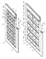
フレームFは、矩形枠状の支持部19と、この支持部19に支持された複数の板状部1Aとを有している。支持部19には、このフレームFを所望の箇所に位置決め固定するのに利用するための適当なサイズの貫通孔(図示略)を設けた構成とすることもできる。各板状部1Aは、最終的にはチップ抵抗器の抵抗体となる部分であり、その長手方向の略全長域にわたって各所の幅および厚みが一定とされた帯状あるいは長矩形状である。複数の板状部1Aは、フレームFに形成された複数のスリット18のそれぞれを介して各板状部1Aの幅方向に略平行に並んでいる。板状部1Aの長手方向両端部と支持部19とを繋ぐ連接部17の幅W1は、各板状部1Aの幅W2よりも小さく形成されている。
【0023】
フレームFは、金属製プレートから製造することができる。すなわち、たとえば図2に示すようなプレートPにパンチングを施すことにより、複数のスリット18を貫通させて形成すると、これによりフレームFが得られる。また、パンチングに代えて、たとえはエッチング処理によってスリット18を形成した場合も同様であり、スリット18を形成する手段としては種々の手段を用いることが可能である。チップ抵抗器のメーカがフレームFを準備する場合、このフレームFを自社において製造してもよいが、これに代えて、たとえば他社から購入してもよいことは勿論である。図1(a)においては、フレームFに4つの板状部1Aが設けられているに過ぎないが、これは理解の容易のためであり、チップ抵抗器の生産性を高める観点からすると、1つのフレームFに多数の板状部1Aが設けられることとなる。
【0024】
次に、上記したフレームFを用いてチップ抵抗器を製造する方法の一例について、図3〜図6を参照して説明する。
【0025】
まず、図3(a)に示すように、各板状部1Aの上向きの片面10aの全体に絶縁層2C'を形成する。図面においては、支持部19上にも絶縁層2C'が形成されているが、この支持部19上には形成する必要はない。絶縁層2C'の形成は、たとえばエポキシ樹脂をベタ塗り状に厚膜印刷して行なう。必要に応じて、この絶縁層2C'の表面には標印を施すことができる。
【0026】
次いで、同図(b)に示すように、フレームFを表裏反転させてから、各板状部1Aの上向きとなった面10bに、複数の絶縁層2Aを各板状部1Aの長手方向に一定間隔で並ぶように形成する。各絶縁層2Aは、各板状部1Aと同一幅を有する矩形状である。各絶縁層2Aの形成は、絶縁層2C'の形成に用いたのと同一の樹脂および装置を用いて厚膜印刷により行なう。このようにすれば、複数種類の材料や装置を用いる場合と比較して、チップ抵抗器の製造コストを削減するのに好ましい。また、上記厚膜印刷の手法によれば、各絶縁層2Aを所望のサイズに正確に仕上げることができる。
【0027】
板状部1Aの一対の側面10cには、後述するように絶縁層2B'を形成するが、そのための前準備として、図4(c) に示すように、各板状部1Aをその長手方向に延びる軸線C1周りの矢印N1方向に略90度回転させる。この回転は、連接部17を捩じり変形させることにより行なう。ただし、連接部17は、板状部1Aと比較して幅狭であるため、この連接部17は捩じり変形し易く、板状部1Aを簡単に回転させることが可能である。
【0028】
このように各板状部1Aを回転させると、一対の側面10cのそれぞれは、その向きが変わり、しかも支持部19の表面よりも上方、または裏面よりも下方に位置することとなる。このため、たとえば同図(d)に示すように、絶縁膜形成用の液状の塗料2B"に板状部1Aの側面10cを接触させることによってこの側面10cに塗料2B"を塗布するといった作業が簡単に、かつ適切に行なえることとなる。塗布された塗料2B"の乾燥硬化により、図5(e)に示すように、各板状部1Aの一対の側面10cには、絶縁層2B'が適切に形成される。もちろん、絶縁層2B'は、塗料を塗布するのとは異なる手法で形成することができる。絶縁層2B'の形成後には、各板状部1Aを逆回転させて元の姿勢に戻しておく。ただし、以降の電極形成や各板状部1Aの切断作業は、各板状部1Aが図4(c)に示されたような回転状態であっても実施可能であり、各板状部1Aを元の姿勢に戻す工程を省略し、全体の工程数の減少を図ってもかまわない。
【0029】
次いで、図5(f)に示すように、各板状部1Aの片面10bのうち、絶縁層2Aどうしの間の領域に、電極3A'とハンダ層39A'とを順次形成する。電極3A'の形成はたとえば銅メッキにより行なう。メッキ処理によれば、電極3A'と絶縁層2Aとの間に隙間を生じさせないようにして、隣り合う絶縁層2A間の領域に電極3A'を均一に形成することが可能である。電極3A'の厚みは、絶縁層2Aの厚みよりも大きくする。ハンダ層39A'の形成も電極3A'と同様に、たとえばメッキ処理によって行なう。このように、電極3A'とハンダ層39A'とを形成することにより、チップ抵抗器が板状部1Aの長手方向に一体的に繋がった構成に相当するバー状の抵抗器集合体A’が得られることとなる。もちろん、本願発明においては、このような工程に代えて、電極3A'の形成後にハンダ層39A'を形成することなく、後述するようなチップ化を図った後に、ハンダ層の形成工程を行なうようにしてもかまわない。
【0030】
その後は、図6に示すように、バー状の各抵抗器集合体A’を同図の仮想線C2で示す箇所において切断し、複数のチップ抵抗器Aに分割する。各チップ抵抗器Aは、板状部1Aが切断されたチップ状の抵抗体1と、電極3A'およびハンダ層39A'が切断された電極3およびハンダ層39と、絶縁層2Aと、絶縁層2B',2C'が切断された絶縁層2B,2Cとを備えたものとなる。
【0031】
より詳しくは、チップ抵抗器Aは、図7〜図10に示すように、チップ状の抵抗体1の裏面10bに、互いに間隔を隔てた一対の電極3およびこれに積層した一対のハンダ層39が設けられ、かつ一対の電極3間には絶縁層2Aが設けられた構成となる。各電極3の厚みt1は、絶縁層2Aの厚みt2よりも大きいものとなっている。抵抗体1の表面10aは、絶縁層2Cにより覆われているとともに、抵抗体1の各側面10cは、絶縁層2Bにより覆われたものとなる。抵抗体1の両端面10dは非被覆状態の露出面となる。
【0032】
各電極3は、絶縁層2Aの幅方向の端面20との間に隙間が生じないように端面20に接している。このことにより、一対の電極3の間隔は、絶縁層2Aによって規定されており、絶縁層2Aの幅s1と同一の寸法となっている。図8においては、電極3やハンダ層39の端部を概略的に示しているが、これら電極3やハンダ層39はメッキにより形成されているために、実際には、図9の符号n1で示すように、それらの一部分は絶縁層2A上にオーバラップしている。ただし、このオーバラップしている部分自体は、抵抗体1の裏面10bに直接接触している訳ではないため、抵抗体1の電極間抵抗値に誤差を生じさせる要因にはならない。
【0033】
チップ抵抗器Aは、所望の実装対象領域に対し、たとえばハンダリフローの手法を用いて面実装される。このハンダリフローの手法では、実装対象領域に設けられている端子上にクリームハンダを塗布してから、その上に各電極3を接触させるようにチップ抵抗器Aを載置した状態で、リフロー炉を利用して加熱する。各電極3は、絶縁層2Aの下面よりも下方に突出しているために、各電極3の下面へのハンダ付着の確実化が図られる。
【0034】
上記面実装時には、ハンダが上記端子からはみ出す場合がある。これに対し、抵抗体1の裏面10bの電極3間の領域と抵抗体1の各側面10cとは、絶縁層2A,2Bにより覆われているために、抵抗体1のそれらの面にハンダが直接付着することはない。したがって、抵抗体1に対する不当なハンダ付着に起因して抵抗値誤差が発生することはない。また、抵抗体1の表面10aは絶縁層2Cによって覆われているために、この表面10aと他の部材や機器との間に不当な電気導通が生じることも防止される。一方、抵抗体1の一対の端面10dは露出しているために、この端面10dに対してはハンダを付着させることによりハンダフィレットを形成し、ハンダ接合強度を高めることが可能である。このハンダフィレットを確実に形成させるための手段として、ハンダ層39と一体または別体のハンダ層を端面10dに形成してもかまわない。
【0035】
抵抗体1は、図1に示したフレームFの板状部1Aを切断することにより形成されたものであるが、そのサイズについては高い寸法精度に仕上げることが可能である。また、一対の電極3間の寸法s1は、絶縁層2Aの幅と一致するが、この絶縁層2Aは厚膜印刷によってかなり高い寸法精度で形成することが可能であるから、上記寸法s1も高い精度で所望の寸法に仕上げることができる。このように、抵抗体1のサイズおよび一対の電極3間の寸法s1が高い精度に仕上げられていれば、このチップ抵抗器Aの電極間抵抗値の誤差を非常に小さくすることが可能である。したがって、このチップ抵抗器Aにおいては、その製造後に、抵抗値調整を行なうためのトリミングを行なう必要を無くすことができる。トリミングを無くすことができれば、その分だけチップ抵抗器Aのコスト低減が図られる。
【0036】
また、上述したチップ抵抗器Aの製造に際しては、従来技術とは異なり、金属板の一部に切削加工を施すことによって一対の電極を形成するといった必要はないため、製造作業の効率も良い。したがって、チップ抵抗器Aのコストをより低減することが可能である。
【0037】
図11〜図13は、本願発明の他の実施形態を示している。これらの図において、上記実施形態と同一または類似の要素には、同一の符号を付している。
【0038】
図11(a),(b)に示すチップ抵抗器Aaは、抵抗体1の裏面10bの両端縁から適当な距離s2 だけ離間した位置に一対の電極3が設けられ、かつ裏面10bのそれ以外の領域には絶縁層2Aが3箇所に分散して設けられた構成を有している(なお、図11〜図13においては、各電極3に積層して形成されるハンダ層39を省略している)。このような構成のチップ抵抗器Aaにおいては、各電極3が抵抗体1の端縁から適当な距離s2だけ離間していることにより、各電極3の幅の縮小化が図られている。このため、一対の電極3のそれぞれの内側端縁30a間の抵抗値R1と、外側端縁30b間の抵抗値R2との差を小さくすることが可能である。したがって、たとえば面実装に用いられるハンダが不均一に塗布されていることに起因して、内側端縁30a寄りに偏った位置でハンダ付けがなされた場合と、外側端縁30b寄りに偏った位置でハンダ付けがなされた場合との抵抗値の差を小さくするのに好適となる。
【0039】
このようなチップ抵抗器Aaを製造するには、たとえば同図(c)に示すように、フレームFの各板状部1Aの片面上に、複数の絶縁層2Aを形成するとともに、それらの間に電極3を形成することにより、バー状の抵抗器集合体Aa'を形成する。次いで、仮想線C3で示す箇所において、この抵抗器集合体Aa'を切断すればよい。
【0040】
図12(a),(b)に示すチップ抵抗器Abは、絶縁層2Aが略十字状に形成されていることにより、抵抗体1の裏面には4つの電極3が設けられている。このチップ抵抗器Abにおいては、4つの電極3を有しているために、たとえば次のような使用が可能となる。すなわち、4つの電極3のうち、2つの電極3を一対の電流用電極として用いるとともに、残りの2つの電極3を一対の電圧用電極として用いる。電気回路の電流検出を行なう場合、一対の電流用電極3については上記電気回路の電流が流れるように上記電気回路との電気接続を図る。一対の電圧用電極3には電圧計を接続する。チップ抵抗器Abの抵抗値は既知であるため、このチップ抵抗器Abの抵抗体1における電圧降下を上記電圧計を利用して測定すると、この測定値をオームの式にあてはめることにより、抵抗体1に流れる電流の値を正確に知ることが可能となる。また、上記した4つの電極3の配置は対称であるから、チップ抵抗器Abを上下反転させて実装しても不具合を生じないようにすることができる。
【0041】
このチップ抵抗器Abを製造するには、たとえばフレームFの片面に形成する絶縁層2Aを同図(c)に示すような形状とするとともに、上記片面の残余部分に電極3を形成することにより、バー状の抵抗器集合体Ab'を形成する。次いで、同図の仮想線C4で示す箇所において抵抗器集合体Ab'を切断すればよい。
【0042】
上記実施形態のように、本願発明においては、二対(4つ)の電極3を設けたチップ抵抗器を製造する構成とすることもできる。もちろん、二対以上の対をなすようにそれ以上の数の電極3を設けた構成としてもかまわない。チップ抵抗器の電極の総数を多くした場合、たとえばそれらのうちの一部の電極のみを使用するといった使用法も可能である。
【0043】
図13(a),(b)に示すチップ抵抗器Acは、2つの電極3aどうし、および2つの電極3bどうしがそれぞれ対をなしており、かつ電極3aと電極3bとは、互いに形状、サイズ、およびそれらの電極間寸法s3,s4が相違したものとなっている。このチップ抵抗器Acを製造するには、たとえばフレームFの各板状部1Aの片面に形成する絶縁層2Aを、同図(c)に示したような形状とするとともに、上記片面の残余部分に電極を3a,3bを形成することにより抵抗器集合体Ac'を形成する。そして、同図の仮想線C5で示す箇所において抵抗器集合体Ac'を切断すればよい。本実施形態から理解されるように、本願発明においては、複数の電極の形状やサイズなどを不揃いにしたチップ抵抗器の製造にも適用することができる。本願発明の製造方法により製造されるチップ抵抗器の電極のそれぞれの具体的な形状、サイズ、および配置などは限定されるものではない。
【0044】
本願発明は、上述した実施形態の内容に限定されない。本願発明に係るチップ抵抗器の製造方法の各作業工程の具体的な構成は、種々に変更自在である。本願発明は、低抵抗のチップ抵抗器の製造に好適であるが、その抵抗値の具体的な値も限定されない。
【0045】
チップ抵抗器の製造に用いるフレームも、上述した実施形態に限定されない。たとえば、図14(a)に示すように、複数の板状部1Aが支持部19に片もち状に支持された形態とすることも可能であり、必ずしも各板状部1Aを支持部19に両端支持させていなくてもかまわない。また、同図(b)に示すように、板状部1Aと支持部19との連接部17を細幅に形成する場合には、板状部1Aの幅方向中心から偏った位置に連接部17を設けた構成としてもかまわない。フレームの材質や板状部の具体的なサイズなどは、最終的に製造されるチップ抵抗器の仕様に応じて適宜選択できる事項である。
【図面の簡単な説明】
【図1】(a)は、本願発明に係るチップ抵抗器の製造に用いられるフレームの一例を示す斜視図であり、(b)は、その要部平面図である。
【図2】図1に示すフレームを製造するためのプレートの斜視図である。
【図3】(a),(b)は、本願発明に係るチップ抵抗器の製造方法の一例の一部の工程を示す斜視図である。
【図4】(c),(d)は、本願発明に係るチップ抵抗器の製造方法の一例の他の工程を示す説明図である。
【図5】(e),(f)は、本願発明に係るチップ抵抗器の製造方法の一例の他の工程を示す斜視図である。
【図6】本願発明に係るチップ抵抗器の製造方法の一例の他の工程を示す斜視図である。
【図7】図3〜図6に示した製造方法により製造されたチップ抵抗器の一例を示す斜視図である。
【図8】図7のVIII−VIII断面図である。
【図9】図8の要部拡大断面図である。
【図10】図7のX−X断面図である。
【図11】(a)は、本願発明に係るチップ抵抗器の他の例を示す断面図であり、(b)は、(a)の底面図であり、(c)は、(a)に示すチップ抵抗器を製造する工程の一例を示す要部平面図である。
【図12】(a)は、本願発明に係るチップ抵抗器の他の例を示す断面図であり、(b)は、(a)の底面図であり、(c)は、(a)に示すチップ抵抗器を製造する工程の一例を示す要部平面図である。
【図13】(a)は、本願発明に係るチップ抵抗器の他の例を示す断面図であり、(b)は、(a)の底面図であり、(c)は、(a)に示すチップ抵抗器を製造する際の工程例を示す要部平面図である。
【図14】(a),(b)は、フレームの他の例を示す要部平面図である。
【図15】従来のチップ抵抗器の一例を示す斜視図である。
【図16】(a)〜(e)は、従来のチップ抵抗器の製造方法の一例を示す説明図である。
【符号の説明】
A,Aa〜Ac チップ抵抗器
F フレーム
1 抵抗体
1A 板状部(フレームの)
2A 絶縁層
2B,2B' 絶縁層
2C,2C' 絶縁層
3,3A' 電極
10a,10b 表裏面
10c 側面[0001]
BACKGROUND OF THE INVENTION
The present invention relates to a chip resistor manufacturing method and a frame used therefor.
[0002]
[Prior art]
An example of a conventional chip resistor is shown in FIG. 15 (see Patent Document 1). The illustrated chip resistor B has a configuration in which a pair of
[0003]
This chip resistor B is manufactured by a method as shown in FIG. First, as shown in FIG. 5A, two
[0004]
[Patent Document 1]
JP 2002-57009 A (FIGS. 1 and 3)
[0005]
[Problems to be solved by the invention]
The chip resistor B described above has a structure in which the region between the pair of
[0006]
Moreover, in the said prior art, there existed a malfunction that the manufacture operation | work of the chip resistor B was complicated and the productivity was bad. More specifically, conventionally, the
[0007]
The present invention has been conceived under the circumstances described above, and it is possible to eliminate or suppress such a problem that an error occurs in the resistance value due to solder adhesion to the resistor. An object of the present invention is to provide a chip resistor manufacturing method capable of efficiently and appropriately manufacturing a chip resistor. Another object of the present invention is to provide a manufacturing frame suitable for carrying out such a chip resistor manufacturing method.
[0008]
DISCLOSURE OF THE INVENTION
In order to solve the above problems, the present invention takes the following technical means.
[0009]
A method of manufacturing a chip resistor provided by the first aspect of the present invention includes a plurality of plate-like portions having front and back surfaces and a pair of side surfaces and extending in a certain direction, and supporting the plurality of plate-like portions. A frame made of a conductive member provided with a support portion is prepared, and a plurality of electrodes arranged at intervals in the predetermined direction on one of the front and back surfaces of each plate-like portion and a region between the plurality of electrodes Forming a plurality of bar-shaped resistor assemblies by forming a second insulating layer on the pair of side surfaces of each plate-like portion, Dividing each resistor assembly into a plurality of chip resistors so that each of the plate-like portions becomes a plurality of chip-like resistors.
[0010]
According to the present invention, a plurality of electrodes are provided on either one of the front and back sides of the chip-like resistor, and the inter-electrode region and the pair of side surfaces of the resistor are the first and second insulating layers. A chip resistor having a structure coated with is manufactured. In the chip resistor having such a structure, there is no possibility that the solder is erroneously attached to the above-described one surface or the pair of side surfaces of the resistor. Therefore, a large error in resistance value due to improper solder adhesion to the resistor is prevented, and a large deviation in the specifications of an electric circuit configured using a chip resistor is properly eliminated. Is done.
[0011]
Further, according to the present invention, unlike the prior art, a plurality of electrodes can be divided by the first insulating layer, and a cutting means is used as a means for forming the plurality of electrodes. There is no need to use. For this reason, unlike the prior art, it is possible to easily prevent the resistor from being cut inappropriately and to make the resistor have a desired accurate size. As a result, according to the present invention, it is possible to manufacture a chip resistor having a very small error and a very high quality.
[0012]
Furthermore, according to the present invention, in addition to being able to take a plurality of chip resistors from each plate-like portion of the frame, the work of forming the second insulating layer is divided into a plurality of chip resistors. Since the corresponding operations can be performed collectively, the production efficiency of the chip resistor is good and the production cost can be reduced.
[0013]
In a preferred embodiment of the present invention, the step of forming the second insulating layer on the pair of side surfaces of each plate-like portion twists the connecting portion between each plate-like portion and the support portion of the frame. By deforming, each plate-like portion is rotated around an axis extending in the longitudinal direction. According to such a structure, when each said plate-shaped part is rotated around the said axis line, the direction of the side surface is changed, and the side surface vicinity part of each said plate-shaped part is said from the support part of the said frame. It can also be made to protrude in the thickness direction of the frame. Therefore, it is possible to facilitate the work of forming the second insulating layer on the side surface of each plate-like portion.
[0014]
In a preferred embodiment of the present invention, a frame in which the connecting part is formed narrower than the plate-like part is used as the frame. According to such a structure, each said connection part becomes easy to torsionally deform, and each said plate-shaped part can be rotated easily.
[0015]
In a preferred embodiment of the present invention, before dividing the resistor assembly into a plurality of chip resistors, the surface on which the first insulating layer is formed among the front and back surfaces of each plate-like portion. The method further includes the step of forming a third insulating layer on the opposite surface. According to such a configuration, a chip resistor in which the surface of the resistor is insulated and protected by the third insulating layer is obtained.
[0016]
In a preferred embodiment of the present invention, in the step of producing the bar-shaped resistor assembly, the first to third insulating layers are formed on the plate-like portions, and then the plurality of the plurality of the plurality of bar-shaped resistor assemblies are plated. Forming an electrode. According to such a configuration, the plurality of electrodes can be easily formed collectively by plating.
[0017]
The frame provided by the second aspect of the present invention includes a plurality of plate-like portions having front and back surfaces and a pair of side surfaces and extending in a certain direction, and a support portion that supports the plurality of plate-like portions. A frame made of a conductive member, wherein the connecting portion between each plate-like portion and the support portion is formed narrower than the plate-like portion.
[0018]
The frame having such a configuration can be suitably used in the implementation of the chip resistor manufacturing method provided by the first aspect of the present invention. In particular, since each of the connecting portions is formed with a narrow width, the operation of rotating the plate-like portions by twisting and deforming the connecting portions can be easily performed.
[0019]
Other features and advantages of the present invention will become more apparent from the following description of embodiments of the invention.
[0020]
DETAILED DESCRIPTION OF THE INVENTION
Hereinafter, a preferred embodiment of the present invention will be specifically described with reference to the drawings.
[0021]
In manufacturing the chip resistor, for example, a frame F as shown in FIG. 1 is prepared in advance. The frame F serves as a resistor material of the chip resistor, and is made of a metal such as a Ni—Cu alloy, a Cu—Mn alloy, or a Ni—Cr alloy. However, the specific material is not limited, and is appropriately selected according to the material of the resistor of the chip resistor to be finally obtained.
[0022]
The frame F has a rectangular frame-shaped
[0023]
The frame F can be manufactured from a metal plate. That is, for example, when a plurality of
[0024]
Next, an example of a method for manufacturing a chip resistor using the above-described frame F will be described with reference to FIGS.
[0025]
First, as shown in FIG. 3A, an insulating
[0026]
Next, as shown in FIG. 6B, after the frame F is turned upside down, a plurality of insulating
[0027]
As will be described later, an insulating
[0028]
When each plate-
[0029]
Next, as shown in FIG. 5 (f), an
[0030]
After that, as shown in FIG. 6, each bar-shaped resistor aggregate A ′ is cut at a location indicated by an imaginary line C <b> 2 in the same figure and divided into a plurality of chip resistors A. Each chip resistor A includes a chip-
[0031]
More specifically, the chip resistor A includes a pair of
[0032]
Each
[0033]
The chip resistor A is surface-mounted on a desired mounting target area using, for example, a solder reflow technique. In this solder reflow technique, cream solder is applied to the terminals provided in the mounting target area, and then the chip resistor A is placed so that each
[0034]
During the surface mounting, the solder may protrude from the terminal. On the other hand, since the region between the
[0035]
The
[0036]
Further, when manufacturing the chip resistor A described above, unlike the prior art, it is not necessary to form a pair of electrodes by cutting a part of a metal plate, so that the efficiency of the manufacturing operation is good. Therefore, the cost of the chip resistor A can be further reduced.
[0037]
11 to 13 show another embodiment of the present invention. In these drawings, elements that are the same as or similar to those in the above embodiment are given the same reference numerals.
[0038]
A chip resistor Aa shown in FIGS. 11 (a) and 11 (b) is provided with a pair of
[0039]
In order to manufacture such a chip resistor Aa, for example, as shown in FIG. 2C, a plurality of insulating
[0040]
In the chip resistor Ab shown in FIGS. 12A and 12B, four
[0041]
In order to manufacture this chip resistor Ab, for example, the insulating
[0042]
Like the said embodiment, in this invention, it can also be set as the structure which manufactures the chip resistor which provided the two pairs (four) of
[0043]
In the chip resistor Ac shown in FIGS. 13A and 13B, two
[0044]
The present invention is not limited to the contents of the above-described embodiment. The specific configuration of each work process of the chip resistor manufacturing method according to the present invention can be variously changed. The present invention is suitable for manufacturing a low-resistance chip resistor, but the specific value of the resistance value is not limited.
[0045]
The frame used for manufacturing the chip resistor is not limited to the above-described embodiment. For example, as shown in FIG. 14 (a), a plurality of plate-
[Brief description of the drawings]
FIG. 1A is a perspective view showing an example of a frame used for manufacturing a chip resistor according to the present invention, and FIG.
2 is a perspective view of a plate for manufacturing the frame shown in FIG. 1. FIG.
FIGS. 3A and 3B are perspective views showing some steps of an example of a method for manufacturing a chip resistor according to the present invention; FIGS.
FIGS. 4C and 4D are explanatory views showing another process of the example of the method for manufacturing the chip resistor according to the present invention. FIGS.
FIGS. 5E and 5F are perspective views showing another process of the example of the method for manufacturing the chip resistor according to the present invention. FIGS.
FIG. 6 is a perspective view showing another process of the example of the chip resistor manufacturing method according to the present invention.
7 is a perspective view showing an example of a chip resistor manufactured by the manufacturing method shown in FIGS. 3 to 6; FIG.
8 is a cross-sectional view taken along the line VIII-VIII in FIG.
9 is an enlarged cross-sectional view of a main part of FIG.
10 is a cross-sectional view taken along the line XX of FIG.
11A is a cross-sectional view showing another example of the chip resistor according to the present invention, FIG. 11B is a bottom view of FIG. 11A, and FIG. It is a principal part top view which shows an example of the process of manufacturing the chip resistor shown.
12A is a cross-sectional view showing another example of the chip resistor according to the present invention, FIG. 12B is a bottom view of FIG. 12A, and FIG. 12C is a cross-sectional view of FIG. It is a principal part top view which shows an example of the process of manufacturing the chip resistor shown.
13A is a cross-sectional view showing another example of a chip resistor according to the present invention, FIG. 13B is a bottom view of FIG. 13A, and FIG. 13C is a cross-sectional view of FIG. It is a principal part top view which shows the process example at the time of manufacturing the chip resistor shown.
FIGS. 14A and 14B are main part plan views showing another example of a frame. FIGS.
FIG. 15 is a perspective view showing an example of a conventional chip resistor.
FIGS. 16A to 16E are explanatory views showing an example of a conventional method of manufacturing a chip resistor.
[Explanation of symbols]
A, Aa to Ac Chip
Claims (6)
上記各板状部の表裏面のいずれか一方に、上記一定方向に間隔を隔てて並んだ複数の電極とこれら複数の電極間領域に位置する第1の絶縁層とを形成するとともに、上記各板状部の一対の側面に第2の絶縁層を形成することにより、複数のバー状の抵抗器集合体を作製する工程と、
上記各板状部を複数のチップ状の抵抗体とするように、上記各抵抗器集合体を複数のチップ抵抗器に分割する工程と、
を有していることを特徴とする、チップ抵抗器の製造方法。Preparing a frame made of a conductive member including a plurality of plate-like portions having front and back surfaces and a pair of side surfaces and extending in a certain direction, and a support portion for supporting the plurality of plate-like portions;
On either one of the front and back surfaces of each plate-like part, a plurality of electrodes arranged at intervals in the predetermined direction and a first insulating layer located in the inter-electrode region are formed, Forming a plurality of bar-shaped resistor assemblies by forming a second insulating layer on a pair of side surfaces of the plate-like portion; and
Dividing each resistor assembly into a plurality of chip resistors so that each plate-like portion is a plurality of chip-like resistors;
A method of manufacturing a chip resistor, comprising:
上記各板状部と上記支持部との連接部は、上記板状部よりも幅狭に形成されていることを特徴とする、フレーム。A frame comprising a conductive member having a plurality of plate-like portions having front and back surfaces and a pair of side surfaces and extending in a certain direction, and a support portion for supporting the plurality of plate-like portions,
The connecting portion between each plate-like portion and the support portion is formed to be narrower than the plate-like portion.
Priority Applications (4)
| Application Number | Priority Date | Filing Date | Title |
|---|---|---|---|
| JP2002348883A JP3653076B2 (en) | 2002-11-29 | 2002-11-29 | Chip resistor manufacturing method and frame used therefor |
| PCT/JP2003/013964 WO2004040592A1 (en) | 2002-10-31 | 2003-10-30 | Chip resistor, process for producing the same, and frame for use therein |
| CN200380102422.XA CN1708814B (en) | 2002-10-31 | 2003-10-30 | Chip resistor, process for producing the same, and frame for use therein |
| US10/533,489 US7612429B2 (en) | 2002-10-31 | 2003-10-30 | Chip resistor, process for producing the same, and frame for use therein |
Applications Claiming Priority (1)
| Application Number | Priority Date | Filing Date | Title |
|---|---|---|---|
| JP2002348883A JP3653076B2 (en) | 2002-11-29 | 2002-11-29 | Chip resistor manufacturing method and frame used therefor |
Publications (2)
| Publication Number | Publication Date |
|---|---|
| JP2004186247A JP2004186247A (en) | 2004-07-02 |
| JP3653076B2 true JP3653076B2 (en) | 2005-05-25 |
Family
ID=32751670
Family Applications (1)
| Application Number | Title | Priority Date | Filing Date |
|---|---|---|---|
| JP2002348883A Expired - Lifetime JP3653076B2 (en) | 2002-10-31 | 2002-11-29 | Chip resistor manufacturing method and frame used therefor |
Country Status (1)
| Country | Link |
|---|---|
| JP (1) | JP3653076B2 (en) |
Families Citing this family (1)
| Publication number | Priority date | Publication date | Assignee | Title |
|---|---|---|---|---|
| JP4526117B2 (en) * | 2004-06-23 | 2010-08-18 | ローム株式会社 | Chip resistor having low resistance value and manufacturing method thereof |
-
2002
- 2002-11-29 JP JP2002348883A patent/JP3653076B2/en not_active Expired - Lifetime
Also Published As
| Publication number | Publication date |
|---|---|
| JP2004186247A (en) | 2004-07-02 |
Similar Documents
| Publication | Publication Date | Title |
|---|---|---|
| TWI260650B (en) | Chip resistor and its manufacturing method | |
| US7327214B2 (en) | Chip resistor and method of making the same | |
| JP4047760B2 (en) | Chip resistor and manufacturing method thereof | |
| US7612429B2 (en) | Chip resistor, process for producing the same, and frame for use therein | |
| JP3848286B2 (en) | Chip resistor | |
| US8044765B2 (en) | Chip resistor and method of making the same | |
| JP4640952B2 (en) | Chip resistor and manufacturing method thereof | |
| JP2004311747A (en) | Chip resistor and its manufacturing method | |
| JP3848247B2 (en) | Chip resistor and manufacturing method thereof | |
| JP3848245B2 (en) | Chip resistor | |
| JP3653076B2 (en) | Chip resistor manufacturing method and frame used therefor | |
| JP5242614B2 (en) | Chip resistor and manufacturing method thereof | |
| JP5490861B2 (en) | Chip resistor and manufacturing method thereof | |
| JP5037288B2 (en) | Chip resistor and manufacturing method thereof | |
| JP2004153160A (en) | Chip resistor and method for manufacturing the same | |
| JP2006157064A (en) | Chip resistor and method of manufacturing the same | |
| JP2004319874A (en) | Chip resistor and its manufacturing method | |
| JP2013254983A (en) | Chip resistor and manufacturing method of the same |
Legal Events
| Date | Code | Title | Description |
|---|---|---|---|
| TRDD | Decision of grant or rejection written | ||
| A01 | Written decision to grant a patent or to grant a registration (utility model) |
Free format text: JAPANESE INTERMEDIATE CODE: A01 Effective date: 20050222 |
|
| A61 | First payment of annual fees (during grant procedure) |
Free format text: JAPANESE INTERMEDIATE CODE: A61 Effective date: 20050224 |
|
| R150 | Certificate of patent or registration of utility model |
Ref document number: 3653076 Country of ref document: JP Free format text: JAPANESE INTERMEDIATE CODE: R150 Free format text: JAPANESE INTERMEDIATE CODE: R150 |
|
| FPAY | Renewal fee payment (event date is renewal date of database) |
Free format text: PAYMENT UNTIL: 20110304 Year of fee payment: 6 |
|
| R250 | Receipt of annual fees |
Free format text: JAPANESE INTERMEDIATE CODE: R250 |
|
| FPAY | Renewal fee payment (event date is renewal date of database) |
Free format text: PAYMENT UNTIL: 20120304 Year of fee payment: 7 |
|
| FPAY | Renewal fee payment (event date is renewal date of database) |
Free format text: PAYMENT UNTIL: 20130304 Year of fee payment: 8 |
|
| FPAY | Renewal fee payment (event date is renewal date of database) |
Free format text: PAYMENT UNTIL: 20140304 Year of fee payment: 9 |
|
| R250 | Receipt of annual fees |
Free format text: JAPANESE INTERMEDIATE CODE: R250 |
|
| R250 | Receipt of annual fees |
Free format text: JAPANESE INTERMEDIATE CODE: R250 |
|
| R250 | Receipt of annual fees |
Free format text: JAPANESE INTERMEDIATE CODE: R250 |
|
| EXPY | Cancellation because of completion of term |