JP5239107B2 - トレンチ絶縁構造形成の間の凹型面形成に関する問題を減少させる方法 - Google Patents
トレンチ絶縁構造形成の間の凹型面形成に関する問題を減少させる方法 Download PDFInfo
- Publication number
- JP5239107B2 JP5239107B2 JP2001168642A JP2001168642A JP5239107B2 JP 5239107 B2 JP5239107 B2 JP 5239107B2 JP 2001168642 A JP2001168642 A JP 2001168642A JP 2001168642 A JP2001168642 A JP 2001168642A JP 5239107 B2 JP5239107 B2 JP 5239107B2
- Authority
- JP
- Japan
- Prior art keywords
- film
- polishing
- silicon
- stop layer
- dielectric material
- Prior art date
- Legal status (The legal status is an assumption and is not a legal conclusion. Google has not performed a legal analysis and makes no representation as to the accuracy of the status listed.)
- Expired - Fee Related
Links
Images


Classifications
-
- H—ELECTRICITY
- H01—ELECTRIC ELEMENTS
- H01L—SEMICONDUCTOR DEVICES NOT COVERED BY CLASS H10
- H01L21/00—Processes or apparatus adapted for the manufacture or treatment of semiconductor or solid state devices or of parts thereof
- H01L21/70—Manufacture or treatment of devices consisting of a plurality of solid state components formed in or on a common substrate or of parts thereof; Manufacture of integrated circuit devices or of parts thereof
- H01L21/71—Manufacture of specific parts of devices defined in group H01L21/70
- H01L21/76—Making of isolation regions between components
- H01L21/762—Dielectric regions, e.g. EPIC dielectric isolation, LOCOS; Trench refilling techniques, SOI technology, use of channel stoppers
- H01L21/76224—Dielectric regions, e.g. EPIC dielectric isolation, LOCOS; Trench refilling techniques, SOI technology, use of channel stoppers using trench refilling with dielectric materials
Landscapes
- Engineering & Computer Science (AREA)
- Physics & Mathematics (AREA)
- Condensed Matter Physics & Semiconductors (AREA)
- General Physics & Mathematics (AREA)
- Manufacturing & Machinery (AREA)
- Computer Hardware Design (AREA)
- Microelectronics & Electronic Packaging (AREA)
- Power Engineering (AREA)
- Element Separation (AREA)
Description
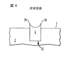
4…トレンチ開口
6…誘電体材料
8…研磨停止層
12…酸化物フィルム
14…ボイド領域
15…縁
26…シリコンフィルム
30…キャップ部分
31…上部表面
39…突端
Claims (9)
- 絶縁トレンチ構造を形成する方法であって、
(a)基材を用意する工程;
(b)前記基材上に研磨停止層を堆積させる工程;
(c)前記研磨停止層の上側表面から前記基材内に下向きに延びる開口を形成し、前記開口を誘電体材料で満たす工程;
(d)前記誘電体材料内部で、かつ、前記研磨停止層の前記上側表面よりも下に存在するボイド領域を形成するように、前記誘電体材料の一部を化学機械研磨で除去する工程;
(e)前記研磨停止層及び前記誘電体材料上にシリコンフィルムを堆積させ、前記ボイド領域を充填する工程;
(f)前記シリコンフィルムを熱的に酸化させ、それによって前記シリコンフィルムを二酸化ケイ素フィルムにする工程;及び
(g)化学機械研磨によって前記研磨停止層上から前記二酸化ケイ素フィルムを除去する工程であって、前記研磨停止層は前記化学機械研磨の停止層として働き、それによって、前記ボイド領域を充填している前記二酸化ケイ素フィルムの上側表面が前記研磨停止層の上側表面と平面になるように、前記ボイド領域を充填している前記二酸化ケイ素フィルムの一部を残すようにする工程;
からなる方法。
- 前記工程(g)が、前記ボイド領域内に残り、かつ、このボイド領域を満たす前記二酸化ケイ素フィルムのキャップ部分を作ることを含み、前記キャップ部分が、前記上側表面と共面の上部表面を有する、請求項1に記載の方法。
- 前記研磨停止層が窒化物フィルムである、請求項1に記載の方法。
- 前記誘電体材料が化学気相堆積によって作られる、請求項1に記載の方法。
- 前記工程(a)が、
(1)窒化ケイ素を含む第1の材料をその上に有する半導体基材を用意する工程であって、前記第1の材料は前記半導体基材上に形成された更なる二酸化ケイ素フィルム上に形成されている、工程;
(2)前記第1の材料及び前記更なる二酸化ケイ素フィルムを通って前記半導体基材内にまで延びる前記開口をエッチングする工程、
(3)前記上側表面上に前記誘電体材料のフィルムを堆積させ、前記開口を充填する工程、及び
(4)前記上側表面上から前記誘電体材料のフィルムの一部を除去し、前記開口内において前記誘電体の上側面が前記上側平面の下にへこんでいるようにし、それによって前記ボイド領域を作る工程、
を含む、請求項1に記載の方法。
- 前記工程(g)の後に、(h)前記第1の材料を除去する工程、を更に含む、請求項5に記載の方法。
- 前記第1の材料が窒化ケイ素を含む、請求項5に記載の方法。
- 前記工程(b)が、多結晶シリコンフィルム及びアモルファスシリコンフィルムのうちの一方を堆積させることを含む、請求項1に記載の方法。
- 前記工程(f)が、550℃〜1,100℃の温度での急速熱焼きなまし及び炉酸化の一方を含む、請求項1に記載の方法。
Applications Claiming Priority (2)
| Application Number | Priority Date | Filing Date | Title |
|---|---|---|---|
| US09/586,384 US6500729B1 (en) | 2000-06-02 | 2000-06-02 | Method for reducing dishing related issues during the formation of shallow trench isolation structures |
| US09/586384 | 2000-06-02 |
Publications (3)
| Publication Number | Publication Date |
|---|---|
| JP2002076110A JP2002076110A (ja) | 2002-03-15 |
| JP2002076110A5 JP2002076110A5 (ja) | 2008-06-26 |
| JP5239107B2 true JP5239107B2 (ja) | 2013-07-17 |
Family
ID=24345514
Family Applications (1)
| Application Number | Title | Priority Date | Filing Date |
|---|---|---|---|
| JP2001168642A Expired - Fee Related JP5239107B2 (ja) | 2000-06-02 | 2001-06-04 | トレンチ絶縁構造形成の間の凹型面形成に関する問題を減少させる方法 |
Country Status (4)
| Country | Link |
|---|---|
| US (1) | US6500729B1 (ja) |
| JP (1) | JP5239107B2 (ja) |
| GB (1) | GB2368460B (ja) |
| TW (1) | TW486780B (ja) |
Families Citing this family (5)
| Publication number | Priority date | Publication date | Assignee | Title |
|---|---|---|---|---|
| US7514336B2 (en) * | 2005-12-29 | 2009-04-07 | Agere Systems Inc. | Robust shallow trench isolation structures and a method for forming shallow trench isolation structures |
| CN105702573B (zh) * | 2014-11-27 | 2019-03-26 | 联华电子股份有限公司 | 平坦化半导体装置的方法 |
| FR3054927B1 (fr) * | 2016-08-04 | 2018-07-13 | Soitec | Procede de fabrication d'une structure de semi-conducteur |
| CN113611663A (zh) * | 2021-08-23 | 2021-11-05 | 上海芯物科技有限公司 | 一种半导体表面平坦化的方法及制得的半导体和用途 |
| US20230129131A1 (en) * | 2021-10-25 | 2023-04-27 | Soitec | Method for manufacturing a semiconductor structure |
Family Cites Families (13)
| Publication number | Priority date | Publication date | Assignee | Title |
|---|---|---|---|---|
| US5189501A (en) | 1988-10-05 | 1993-02-23 | Sharp Kabushiki Kaisha | Isolator for electrically isolating semiconductor devices in an integrated circuit |
| JP2597022B2 (ja) | 1990-02-23 | 1997-04-02 | シャープ株式会社 | 素子分離領域の形成方法 |
| US5376222A (en) * | 1991-09-04 | 1994-12-27 | Fujitsu Limited | Polishing method for polycrystalline silicon |
| JP3265199B2 (ja) * | 1996-09-30 | 2002-03-11 | 株式会社東芝 | 化学的機械研磨法、化学的機械研磨法に用いる研磨剤および半導体装置の製造方法 |
| JP3904676B2 (ja) * | 1997-04-11 | 2007-04-11 | 株式会社ルネサステクノロジ | トレンチ型素子分離構造の製造方法およびトレンチ型素子分離構造 |
| US5872045A (en) * | 1997-07-14 | 1999-02-16 | Industrial Technology Research Institute | Method for making an improved global planarization surface by using a gradient-doped polysilicon trench--fill in shallow trench isolation |
| US6136664A (en) * | 1997-08-07 | 2000-10-24 | International Business Machines Corporation | Filling of high aspect ratio trench isolation |
| JPH1187487A (ja) * | 1997-09-03 | 1999-03-30 | Oki Electric Ind Co Ltd | 選択酸化方法 |
| JPH11284061A (ja) * | 1998-03-31 | 1999-10-15 | Kawasaki Steel Corp | 半導体装置の製造方法 |
| US6303461B1 (en) | 1998-12-23 | 2001-10-16 | United Microelectronics Corp. | Method for fabricating a shallow trench isolation structure |
| JP3450221B2 (ja) | 1999-04-21 | 2003-09-22 | Necエレクトロニクス株式会社 | 半導体装置の製造方法 |
| TW429514B (en) * | 1999-10-06 | 2001-04-11 | Mosel Vitelic Inc | Planarization method for polysilicon layer deposited on the trench |
| US6316331B1 (en) * | 2000-10-13 | 2001-11-13 | Vanguard International Semiconductor Corp. | Method of making dishing-free insulator in trench isolation |
-
2000
- 2000-06-02 US US09/586,384 patent/US6500729B1/en not_active Expired - Lifetime
-
2001
- 2001-06-04 TW TW090113472A patent/TW486780B/zh not_active IP Right Cessation
- 2001-06-04 GB GB0113492A patent/GB2368460B/en not_active Expired - Fee Related
- 2001-06-04 JP JP2001168642A patent/JP5239107B2/ja not_active Expired - Fee Related
Also Published As
| Publication number | Publication date |
|---|---|
| GB0113492D0 (en) | 2001-07-25 |
| US6500729B1 (en) | 2002-12-31 |
| JP2002076110A (ja) | 2002-03-15 |
| TW486780B (en) | 2002-05-11 |
| GB2368460B (en) | 2005-01-05 |
| GB2368460A (en) | 2002-05-01 |
Similar Documents
| Publication | Publication Date | Title |
|---|---|---|
| US7915173B2 (en) | Shallow trench isolation structure having reduced dislocation density | |
| US5945724A (en) | Trench isolation region for semiconductor device | |
| US8580649B2 (en) | Method for manufacturing semiconductor device | |
| US7622769B2 (en) | Isolation trench | |
| US5885883A (en) | Methods of forming trench-based isolation regions with reduced susceptibility to edge defects | |
| US5956598A (en) | Method for fabricating a shallow-trench isolation structure with a rounded corner in integrated circuit | |
| US6194283B1 (en) | High density trench fill due to new spacer fill method including isotropically etching silicon nitride spacers | |
| US7238586B2 (en) | Seamless trench fill method utilizing sub-atmospheric pressure chemical vapor deposition technique | |
| US6583025B2 (en) | Method of forming a trench isolation structure comprising annealing the oxidation barrier layer thereof in a furnace | |
| US6399461B1 (en) | Addition of planarizing dielectric layer to reduce a dishing phenomena experienced during a chemical mechanical procedure used in the formation of shallow trench isolation regions | |
| KR19990084517A (ko) | 트렌치 격리 형성 방법 | |
| US20070072387A1 (en) | Method of fabricating shallow trench isolation structure | |
| JP2006156471A (ja) | 半導体装置および半導体装置の製造方法 | |
| JP2000012676A (ja) | 半導体装置のトレンチ素子分離方法 | |
| US6841851B2 (en) | Semiconductor device having a high density plasma oxide layer | |
| US6521510B1 (en) | Method for shallow trench isolation with removal of strained island edges | |
| JP3701175B2 (ja) | 半導体集積回路のトレンチ分離方法 | |
| US6583488B1 (en) | Low density, tensile stress reducing material for STI trench fill | |
| US7029987B2 (en) | Method of manufacturing semiconductor device having shallow trench isolation (STI) | |
| US6649488B2 (en) | Method of shallow trench isolation | |
| US6358785B1 (en) | Method for forming shallow trench isolation structures | |
| JP5239107B2 (ja) | トレンチ絶縁構造形成の間の凹型面形成に関する問題を減少させる方法 | |
| JP2004014696A (ja) | 半導体装置の製造方法 | |
| US7154159B2 (en) | Trench isolation structure and method of forming the same | |
| US6303467B1 (en) | Method for manufacturing trench isolation |
Legal Events
| Date | Code | Title | Description |
|---|---|---|---|
| A521 | Request for written amendment filed |
Free format text: JAPANESE INTERMEDIATE CODE: A523 Effective date: 20080513 |
|
| A621 | Written request for application examination |
Free format text: JAPANESE INTERMEDIATE CODE: A621 Effective date: 20080513 |
|
| RD03 | Notification of appointment of power of attorney |
Free format text: JAPANESE INTERMEDIATE CODE: A7423 Effective date: 20080605 |
|
| RD04 | Notification of resignation of power of attorney |
Free format text: JAPANESE INTERMEDIATE CODE: A7424 Effective date: 20080605 |
|
| A977 | Report on retrieval |
Free format text: JAPANESE INTERMEDIATE CODE: A971007 Effective date: 20111208 |
|
| A131 | Notification of reasons for refusal |
Free format text: JAPANESE INTERMEDIATE CODE: A131 Effective date: 20111226 |
|
| A601 | Written request for extension of time |
Free format text: JAPANESE INTERMEDIATE CODE: A601 Effective date: 20120323 |
|
| A602 | Written permission of extension of time |
Free format text: JAPANESE INTERMEDIATE CODE: A602 Effective date: 20120328 |
|
| A601 | Written request for extension of time |
Free format text: JAPANESE INTERMEDIATE CODE: A601 Effective date: 20120426 |
|
| A602 | Written permission of extension of time |
Free format text: JAPANESE INTERMEDIATE CODE: A602 Effective date: 20120502 |
|
| A521 | Request for written amendment filed |
Free format text: JAPANESE INTERMEDIATE CODE: A523 Effective date: 20120625 |
|
| A131 | Notification of reasons for refusal |
Free format text: JAPANESE INTERMEDIATE CODE: A131 Effective date: 20120731 |
|
| A601 | Written request for extension of time |
Free format text: JAPANESE INTERMEDIATE CODE: A601 Effective date: 20121031 |
|
| A602 | Written permission of extension of time |
Free format text: JAPANESE INTERMEDIATE CODE: A602 Effective date: 20121105 |
|
| A601 | Written request for extension of time |
Free format text: JAPANESE INTERMEDIATE CODE: A601 Effective date: 20121130 |
|
| A602 | Written permission of extension of time |
Free format text: JAPANESE INTERMEDIATE CODE: A602 Effective date: 20121205 |
|
| A521 | Request for written amendment filed |
Free format text: JAPANESE INTERMEDIATE CODE: A523 Effective date: 20130128 |
|
| TRDD | Decision of grant or rejection written | ||
| A01 | Written decision to grant a patent or to grant a registration (utility model) |
Free format text: JAPANESE INTERMEDIATE CODE: A01 Effective date: 20130219 |
|
| A711 | Notification of change in applicant |
Free format text: JAPANESE INTERMEDIATE CODE: A712 Effective date: 20130318 |
|
| A61 | First payment of annual fees (during grant procedure) |
Free format text: JAPANESE INTERMEDIATE CODE: A61 Effective date: 20130318 |
|
| FPAY | Renewal fee payment (event date is renewal date of database) |
Free format text: PAYMENT UNTIL: 20160412 Year of fee payment: 3 |
|
| R150 | Certificate of patent or registration of utility model |
Free format text: JAPANESE INTERMEDIATE CODE: R150 |
|
| S111 | Request for change of ownership or part of ownership |
Free format text: JAPANESE INTERMEDIATE CODE: R313113 |
|
| S533 | Written request for registration of change of name |
Free format text: JAPANESE INTERMEDIATE CODE: R313533 |
|
| R350 | Written notification of registration of transfer |
Free format text: JAPANESE INTERMEDIATE CODE: R350 |
|
| R371 | Transfer withdrawn |
Free format text: JAPANESE INTERMEDIATE CODE: R371 |
|
| S111 | Request for change of ownership or part of ownership |
Free format text: JAPANESE INTERMEDIATE CODE: R313113 |
|
| R371 | Transfer withdrawn |
Free format text: JAPANESE INTERMEDIATE CODE: R371 |
|
| S111 | Request for change of ownership or part of ownership |
Free format text: JAPANESE INTERMEDIATE CODE: R313113 |
|
| R350 | Written notification of registration of transfer |
Free format text: JAPANESE INTERMEDIATE CODE: R350 |
|
| R250 | Receipt of annual fees |
Free format text: JAPANESE INTERMEDIATE CODE: R250 |
|
| LAPS | Cancellation because of no payment of annual fees |