JP5227411B2 - Charge pump circuit and semiconductor integrated circuit - Google Patents
Charge pump circuit and semiconductor integrated circuit Download PDFInfo
- Publication number
- JP5227411B2 JP5227411B2 JP2010529701A JP2010529701A JP5227411B2 JP 5227411 B2 JP5227411 B2 JP 5227411B2 JP 2010529701 A JP2010529701 A JP 2010529701A JP 2010529701 A JP2010529701 A JP 2010529701A JP 5227411 B2 JP5227411 B2 JP 5227411B2
- Authority
- JP
- Japan
- Prior art keywords
- current
- circuit
- charge pump
- voltage
- power supply
- Prior art date
- Legal status (The legal status is an assumption and is not a legal conclusion. Google has not performed a legal analysis and makes no representation as to the accuracy of the status listed.)
- Active
Links
- 239000004065 semiconductor Substances 0.000 title claims description 16
- 239000003990 capacitor Substances 0.000 claims description 58
- 238000001514 detection method Methods 0.000 claims description 4
- 239000000758 substrate Substances 0.000 claims description 3
- 101100407828 Neurospora crassa (strain ATCC 24698 / 74-OR23-1A / CBS 708.71 / DSM 1257 / FGSC 987) ptr-3 gene Proteins 0.000 description 26
- 102100040862 Dual specificity protein kinase CLK1 Human genes 0.000 description 25
- 101000749294 Homo sapiens Dual specificity protein kinase CLK1 Proteins 0.000 description 25
- 238000010586 diagram Methods 0.000 description 25
- 102100040844 Dual specificity protein kinase CLK2 Human genes 0.000 description 18
- 101000749291 Homo sapiens Dual specificity protein kinase CLK2 Proteins 0.000 description 18
- 101100351735 Neurospora crassa (strain ATCC 24698 / 74-OR23-1A / CBS 708.71 / DSM 1257 / FGSC 987) ptr-4 gene Proteins 0.000 description 14
- 230000007423 decrease Effects 0.000 description 11
- 230000002596 correlated effect Effects 0.000 description 8
- 238000012544 monitoring process Methods 0.000 description 8
- 101100349268 Caenorhabditis elegans ntr-2 gene Proteins 0.000 description 7
- 101100388504 Chlamydomonas reinhardtii ODA4 gene Proteins 0.000 description 6
- 101100445488 Neurospora crassa (strain ATCC 24698 / 74-OR23-1A / CBS 708.71 / DSM 1257 / FGSC 987) ptr-2 gene Proteins 0.000 description 6
- 101100119048 Ogataea pini SUP2 gene Proteins 0.000 description 6
- 101100065564 Saccharomyces cerevisiae (strain ATCC 204508 / S288c) SUP35 gene Proteins 0.000 description 6
- 101100389631 Saccharomyces cerevisiae (strain ATCC 204508 / S288c) SUP45 gene Proteins 0.000 description 6
- 230000000875 corresponding effect Effects 0.000 description 6
- 230000000694 effects Effects 0.000 description 6
- 101100349264 Caenorhabditis elegans ntr-1 gene Proteins 0.000 description 4
- 101100215778 Neurospora crassa (strain ATCC 24698 / 74-OR23-1A / CBS 708.71 / DSM 1257 / FGSC 987) ptr-1 gene Proteins 0.000 description 4
- 238000000034 method Methods 0.000 description 4
- 238000012546 transfer Methods 0.000 description 4
- 238000005516 engineering process Methods 0.000 description 3
- 238000009825 accumulation Methods 0.000 description 2
- 230000005540 biological transmission Effects 0.000 description 2
- 230000010355 oscillation Effects 0.000 description 2
- 230000003321 amplification Effects 0.000 description 1
- 239000000919 ceramic Substances 0.000 description 1
- 230000000295 complement effect Effects 0.000 description 1
- 230000001276 controlling effect Effects 0.000 description 1
- 239000013078 crystal Substances 0.000 description 1
- 238000012986 modification Methods 0.000 description 1
- 230000004048 modification Effects 0.000 description 1
- 238000003199 nucleic acid amplification method Methods 0.000 description 1
- 238000012545 processing Methods 0.000 description 1
- -1 respectively Proteins 0.000 description 1
Images


Classifications
-
- H—ELECTRICITY
- H01—ELECTRIC ELEMENTS
- H01L—SEMICONDUCTOR DEVICES NOT COVERED BY CLASS H10
- H01L27/00—Devices consisting of a plurality of semiconductor or other solid-state components formed in or on a common substrate
- H01L27/02—Devices consisting of a plurality of semiconductor or other solid-state components formed in or on a common substrate including semiconductor components specially adapted for rectifying, oscillating, amplifying or switching and having at least one potential-jump barrier or surface barrier; including integrated passive circuit elements with at least one potential-jump barrier or surface barrier
- H01L27/0203—Particular design considerations for integrated circuits
- H01L27/0214—Particular design considerations for integrated circuits for internal polarisation, e.g. I2L
- H01L27/0218—Particular design considerations for integrated circuits for internal polarisation, e.g. I2L of field effect structures
- H01L27/0222—Charge pumping, substrate bias generation structures
-
- H—ELECTRICITY
- H02—GENERATION; CONVERSION OR DISTRIBUTION OF ELECTRIC POWER
- H02M—APPARATUS FOR CONVERSION BETWEEN AC AND AC, BETWEEN AC AND DC, OR BETWEEN DC AND DC, AND FOR USE WITH MAINS OR SIMILAR POWER SUPPLY SYSTEMS; CONVERSION OF DC OR AC INPUT POWER INTO SURGE OUTPUT POWER; CONTROL OR REGULATION THEREOF
- H02M3/00—Conversion of dc power input into dc power output
- H02M3/02—Conversion of dc power input into dc power output without intermediate conversion into ac
- H02M3/04—Conversion of dc power input into dc power output without intermediate conversion into ac by static converters
- H02M3/06—Conversion of dc power input into dc power output without intermediate conversion into ac by static converters using resistors or capacitors, e.g. potential divider
- H02M3/07—Conversion of dc power input into dc power output without intermediate conversion into ac by static converters using resistors or capacitors, e.g. potential divider using capacitors charged and discharged alternately by semiconductor devices with control electrode, e.g. charge pumps
Description
本発明は、被駆動回路に電源を供給するチャージ・ポンプ回路に係り、特に、キャパシタに電荷を蓄積するときに発生するノイズを小さくするのに好適なチャージ・ポンプ回路及び半導体集積回路に関する。 The present invention relates to a charge pump circuit that supplies power to a driven circuit, and more particularly to a charge pump circuit and a semiconductor integrated circuit that are suitable for reducing noise generated when charges are accumulated in a capacitor.
従来、単電源すなわち一つの正電源下で駆動され、グランド終端される小抵抗に対して信号を出力する回路として、図13に示すようなビデオアンプを駆動するチャージ・ポンプ回路の技術が特許文献1に開示されている。この従来技術は、正電源(VCC)とグランド電圧(GND)からチャージ・ポンプ回路で負電源(VEE)を発生し、正電源(VCC)と負電源(VEE)との間で駆動される被駆動回路で、グランド電圧(GND)を中心レベルとしてDC(直流)カット用のキャパシタを用いずに直接負荷を駆動し、信号を出力するものである。 Conventionally, as a circuit that outputs a signal to a small resistor that is driven under a single power source, that is, a single positive power source and is ground-terminated, a technology of a charge pump circuit that drives a video amplifier as shown in FIG. 1 is disclosed. In this prior art, a negative power source (VEE) is generated by a charge pump circuit from a positive power source (VCC) and a ground voltage (GND) and driven between the positive power source (VCC) and the negative power source (VEE). A drive circuit drives a load directly with a ground voltage (GND) as a central level without using a DC (direct current) cut capacitor, and outputs a signal.
ここで用いられるチャージ・ポンプ回路は、クロック信号の第1の期間で与えられた正電圧とグランド電圧の間にキャパシタを直接接続して電荷を蓄積し、第2の期間でグランド電圧と負電圧を発生する負電圧端子の間で該キャパシタを直接接続して、蓄積された電荷を転送させる。この一連の動作を繰り返し行うことで負電圧を発生する。
このチャージ・ポンプ回路において、キャパシタに電荷を蓄積する期間における電流量は、期間の前半は大きいが時間の経過と共に減少し、期間の後半は小さくなる。ビデオアンプ及びその負荷で消費する電流量が大きいときは、この期間の前半に流れる大きな電流が原因となって、電源ノイズ、電流供給能力の超過などの問題が発生する。The charge pump circuit used here stores a charge by directly connecting a capacitor between a positive voltage applied during the first period of the clock signal and the ground voltage, and the ground voltage and negative voltage during the second period. The capacitor is directly connected between the negative voltage terminals that generate the voltage to transfer the accumulated charge. A negative voltage is generated by repeating this series of operations.
In this charge pump circuit, the amount of current during the period in which charges are accumulated in the capacitor is large in the first half of the period but decreases with the passage of time, and becomes smaller in the second half of the period. When the amount of current consumed by the video amplifier and its load is large, problems such as power supply noise and excess current supply capability occur due to the large current flowing in the first half of this period.
この問題を解決するための技術として、図14に示すビデオアンプを駆動するチャージ・ポンプ回路の技術が特許文献2に開示されている。この技術では、チャージ・ポンプ回路のキャパシタに電荷を蓄積する期間における電流量を一定にすることを行う。この技術は、ビデオアンプで消費する電流の大きさに関わらず、内部の定電流回路を用いて一定の電流を作り出し、この定電流でキャパシタに電荷を蓄積するため、電荷を蓄積する期間の前半と後半で同等の電流が流れ、期間の前半だけに大きな電流が流れることを防ぐことができる。
As a technique for solving this problem,
しかしながら、上記特許文献2の従来技術においては、ビデオアンプで消費する電流量の大きさに関わらず、キャパシタに電荷を蓄積する電流が一定であることから、この定電流値はビデオアンプで消費する電流が最大の時にチャージ・ポンプ回路が問題なく動作できる大きめの値に設定する必要があった。そのため、通常使用範囲では必要以上に大きな電流が流れるため、電源ノイズが大きくなり、さらに、電源としては、大きな電流供給能力のあるものが必要であった。
However, in the prior art of
そこで、本発明は、このような従来の技術の有する未解決の課題に着目してなされたものであって、電源を発生し、発生された電源で被駆動回路を駆動するチャージ・ポンプ回路において、チャージ・ポンプ回路のキャパシタに電荷を蓄積するときに発生するノイズを小さくするのに好適なチャージ・ポンプ回路及び半導体集積回路を提供することを目的とするものである。 Accordingly, the present invention has been made paying attention to such an unsolved problem of the conventional technology, and in a charge pump circuit that generates a power source and drives a driven circuit with the generated power source. An object of the present invention is to provide a charge pump circuit and a semiconductor integrated circuit suitable for reducing noise generated when charge is accumulated in a capacitor of a charge pump circuit.
〔発明1〕上記目的を達成するために、発明1のチャージ・ポンプ回路は、入力電源からの電荷をキャパシタに蓄積する第1の状態と前記キャパシタに蓄積された電荷を電源供給部に転送する第2の状態とを交互に繰り返すことで所定の極性の出力電源を生成するチャージ・ポンプ回路であって、前記出力電源で駆動されるアンプ回路の出力段を構成する複数のトランジスタのうち、前記出力電源側のトランジスタの出力電流である第1の電流に比例する第2の電流を発生する、前記第1の電流とカレントミラーの関係にある電流発生部と、該電流発生部において発生した第2の電流に基づき、前記キャパシタに電荷を蓄積するときの電流の供給量を制御する供給電流量制御手段と、を備える。
[Invention 1] In order to achieve the above object, the charge pump circuit of
このような構成であれば、供給電流量制御手段において、出力電源で駆動されるアンプ回路の出力段を構成する複数のトランジスタのうち、出力電源側のトランジスタに流れる電流の量(以下、電流量と称す)の増減に追随して、キャパシタに供給する電流量(以下、供給電流量と称す)を増減する制御を行うことが可能である。
これによって、アンプ回路で消費される電流量と、キャパシタに電荷を蓄積する(以下、充電と称す)ときの供給電流量との差を小さくすることができるので、アンプ回路に電流を過供給するのを防ぐことができると共に、キャパシタを充電するときに発生するノイズを小さくすることができるという効果が得られる。
With such a configuration, in the supply current amount control means, the amount of current flowing through the transistor on the output power source side (hereinafter referred to as current amount) among the plurality of transistors constituting the output stage of the amplifier circuit driven by the output power The amount of current supplied to the capacitor (hereinafter referred to as supply current amount) can be controlled to increase or decrease following the increase or decrease of
As a result, the difference between the amount of current consumed in the amplifier circuit and the amount of supply current when the electric charge is stored in the capacitor (hereinafter referred to as charging) can be reduced, so that the current is excessively supplied to the amplifier circuit. it is possible to prevent the, Ru effect is obtained that it is possible to reduce the noise generated when charging the capacitor.
〔発明2〕 更に、発明2のチャージ・ポンプ回路は、発明1のチャージ・ポンプ回路において、前記供給電流量制御手段は、前記キャパシタに供給する電流の量を、該電流の量と前記被駆動回路に流れる電流の量との間に正の相関が成立するように制御する。
このような構成であれば、発明1と同等の作用及び効果を得ることができる。[Invention 2] The charge pump circuit of
With such a configuration, it is possible to obtain operations and effects equivalent to those of the first aspect.
〔発明3〕 更に、発明3のチャージ・ポンプ回路は、発明1又は2のチャージ・ポンプ回路において、前記供給電流量制御手段は、前記キャパシタに供給する電流の量を、該電流の量が前記被駆動回路に流れる電流の量よりも予め設定された量だけ多くなるように制御する。
このような構成であれば、供給電流量に余裕を持たせることができるので、負荷(被駆動回路)に流れる電流量が0のときや、負荷に流れる電流量がばらついて供給電流量の追随が間に合わないときなどにおいても、チャージ・ポンプ回路を正常に動作させることができるという効果が得られる。[Invention 3] Further, the charge pump circuit of Invention 3 is the charge pump circuit of
With such a configuration, a margin can be provided for the amount of supplied current, so that when the amount of current flowing through the load (driven circuit) is zero or when the amount of current flowing through the load varies, the amount of supplied current can be followed. Even when the time is not in time, the charge pump circuit can be operated normally.
〔発明4〕 更に、発明4のチャージ・ポンプ回路は、発明1乃至3のいずれか1のチャージ・ポンプ回路において、前記キャパシタの両端間の電圧を検出する電圧検出手段と、前記電圧検出手段で検出された電圧のレベルと所定のレベルとを比較する電圧レベル比較手段と、前記電圧レベル比較手段の比較結果に基づき、前記第1の状態において前記検出された電圧のレベルが前記所定のレベルに到達したときに、前記第1の状態を前記第2の状態に切り替える切替制御手段と、を備える。
このような構成であれば、キャパシタの両端間の電圧のレベルが所定のレベルに到達するまではキャパシタを充電し、所定のレベルに到達したときに、キャパシタの充電を止めて、充電された電荷の転送を行わせることができる。
これによって、所定のレベルを所望の電圧のレベルに設定することで、所望の電圧の出力電源を生成することができるという効果が得られる。[Invention 4] The charge pump circuit according to Invention 4 is the charge pump circuit according to any one of
In such a configuration, the capacitor is charged until the voltage level across the capacitor reaches a predetermined level, and when the voltage reaches the predetermined level, the capacitor is stopped and the charged electric charge is stopped. Can be transferred.
As a result, by setting the predetermined level to a desired voltage level, it is possible to produce an output power supply having a desired voltage.
〔発明5〕 更に、発明5のチャージ・ポンプ回路は、発明1乃至4のいずれか1のチャージ・ポンプ回路において、前記供給電流量制御手段は、複数の前記被駆動回路を駆動するときに、前記複数の被駆動回路に流れる電流の量の総和に基づき、前記キャパシタに電荷を蓄積するときの電流の供給量を制御する。
このような構成であれば、供給電流量制御手段において、例えば、複数の被駆動回路に流れる電流量の総和の増減に追随して、キャパシタの供給電流量を増減する制御を行うことが可能である。
これによって、複数の被駆動回路で消費される電流量の総和と、キャパシタを充電するときの供給電流量との差を小さくすることができるので、複数の被駆動回路に対して電流を過供給するのを防ぐことができると共に、キャパシタを充電するときに発生するノイズを小さくすることができるという効果が得られる。[Invention 5] The charge pump circuit of Invention 5 is the charge pump circuit of any one of
With such a configuration, the supply current amount control means can perform control to increase or decrease the supply current amount of the capacitor, for example, following the increase or decrease of the sum of the current amounts flowing in the plurality of driven circuits. is there.
As a result, the difference between the total amount of current consumed by the plurality of driven circuits and the amount of supply current when charging the capacitor can be reduced, so that overcurrent is supplied to the plurality of driven circuits. It is possible to prevent the noise from occurring and to reduce the noise generated when the capacitor is charged.
〔発明6〕 更に、発明6のチャージ・ポンプ回路は、発明1乃至5のいずれか1のチャージ・ポンプ回路において、前記供給電流量制御手段は、前記被駆動回路の出力部に流れる電流の量に基づき、前記キャパシタに電荷を蓄積するときの電流の供給量を制御する。
このような構成であれば、被駆動回路の出力部に流れる電流の量に基づきキャパシタの供給電流量を制御することができるので、出力部に流れる電流をチャージ・ポンプ回路にフィードバックすることで、比較的簡易な構成で供給電流量の制御を行うことができるという効果が得られる。[Invention 6] The charge pump circuit according to
With such a configuration, the amount of current supplied to the capacitor can be controlled based on the amount of current flowing to the output section of the driven circuit, so by feeding back the current flowing to the output section to the charge pump circuit, The effect that the amount of supplied current can be controlled with a relatively simple configuration is obtained.
〔発明7〕 更に、発明7のチャージ・ポンプ回路は、発明1乃至6のいずれか1のチャージ・ポンプ回路において、前記被駆動回路がアンプ回路である。
このような構成であれば、被駆動回路がアンプ回路であることから、容易に半導体集積回路で実現することができるという効果が得られる。[Invention 7] The charge pump circuit according to Invention 7 is the charge pump circuit according to any one of
With such a configuration, since the driven circuit is an amplifier circuit, an effect that it can be easily realized by a semiconductor integrated circuit is obtained.
〔発明8〕 更に、発明8のチャージ・ポンプ回路は、発明1乃至7のいずれか1のチャージ・ポンプ回路において、前記供給電流量制御手段は、前記アンプ回路の出力段の出力電流である第1の電流に比例する第2の電流を発生する、前記第1の電流とカレントミラーの関係にある電流発生部を備え、該電流発生部において発生した第2の電流に基づき、前記第1の状態において前記キャパシタに電荷を蓄積するときの電流の供給量を制御する。
このような構成であれば、アンプ回路から負荷に流れる第1の電流に比例した第2の電流の電流量に基づきキャパシタに供給する供給電流量を制御することができる。[Invention 8] The charge pump circuit according to
With such a configuration, it is possible to control the supply current amount supplied to the capacitor based on the current amount of the second current proportional to the first current flowing from the amplifier circuit to the load.
従って、第1の電流の電流量の増減に追随して、キャパシタに供給する供給電流量を増減する制御を容易に行うことが可能である。
これによって、被駆動回路に対する負荷で消費される電流量と、キャパシタに供給する供給電流量との差を小さくすることができるので、被駆動回路に電流を過供給するのを防ぐことができると共に、キャパシタを充電するときに発生するノイズを小さくすることができるという効果が得られる。Accordingly, it is possible to easily perform control to increase or decrease the amount of current supplied to the capacitor following the increase or decrease of the current amount of the first current.
As a result, the difference between the amount of current consumed by the load on the driven circuit and the amount of supply current supplied to the capacitor can be reduced, so that it is possible to prevent overcurrent supply to the driven circuit. The effect that the noise generated when the capacitor is charged can be reduced is obtained.
〔発明9〕 更に、発明9のチャージ・ポンプ回路は、発明1乃至8のいずれか1のチャージ・ポンプ回路において、前記入力電源から、該入力電源の極性とは反対の極性の出力電源を生成し、前記電源供給部は、前記出力電源と、前記出力電源とは反対の極性の電源との間の電圧範囲の電源を前記被駆動回路に供給する構成となっている。
このような構成であれば、電源供給部において、例えば、グランド電圧を基準にして、入力電源と同極の正電圧の電源と、当該チャージ・ポンプ回路で生成した負電圧の電源とを被駆動回路に供給することが可能である。
これによって、グランド電圧を基準として、正電源及び負電源の双方を用いて駆動する被駆動回路を駆動させることができるという効果が得られる。[Invention 9] The charge pump circuit according to Invention 9 is the charge pump circuit according to any one of
With such a configuration, the power supply unit drives, for example, a positive voltage power supply having the same polarity as the input power supply and a negative voltage power supply generated by the charge pump circuit with reference to the ground voltage. It is possible to supply the circuit.
As a result, it is possible to drive a driven circuit that is driven using both the positive power source and the negative power source with the ground voltage as a reference.
〔発明10〕 一方、上記目的を達成するために、発明10の半導体集積回路は、発明1乃至9のいずれか1項に記載のチャージ・ポンプ回路を含んでなる回路を半導体基板上に集積化して成る。
このような構成であれば、上記発明1乃至9のいずれか1に記載のチャージ・ポンプ回路と同等の作用及び効果が得られる半導体集積回路を得ることができる。[Invention 10] On the other hand, in order to achieve the above object, a semiconductor integrated circuit according to
With such a configuration, it is possible to obtain a semiconductor integrated circuit capable of obtaining the same operation and effect as the charge pump circuit according to any one of the first to ninth aspects.
〔第1の実施の形態〕
以下、本発明の第1の実施の形態を図面に基づき説明する。図1〜図6は、本発明に係るチャージ・ポンプ回路及び半導体集積回路の第1の実施の形態を示す図である。
本実施の形態では、本発明に係るチャージ・ポンプ回路を、被駆動回路であるアンプ回路に適用し、このアンプ回路によって入力信号を増幅して負荷に供給するシステムを構成する。[First Embodiment]
Hereinafter, a first embodiment of the present invention will be described with reference to the drawings. 1 to 6 are diagrams showing a first embodiment of a charge pump circuit and a semiconductor integrated circuit according to the present invention.
In the present embodiment, the charge pump circuit according to the present invention is applied to an amplifier circuit which is a driven circuit, and a system in which an input signal is amplified by this amplifier circuit and supplied to a load is configured.
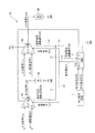
まず、本発明に係る負荷駆動システム1の構成を図1に基づき説明する。図1は、本発明の第1の実施の形態に係る負荷駆動システム1の構成を示すブロック図である。
負荷駆動システム1は、図1に示すように、チャージ・ポンプ回路2と、クロック発生回路4と、アンプ回路6と、負荷8とを含んで構成される。
チャージ・ポンプ回路2は、キャパシタとスイッチング素子とを用いたチャージ・ポンプ方式によって、正極の入力電源VCCから負極の出力電源VEEを生成し、この生成する機能を有している。この生成したVEEはアンプ回路6に供給される。First, the structure of the
As shown in FIG. 1, the
The
クロック発生回路4は、水晶振動子、セラミック振動子などの振動子を備え、チャージ・ポンプ回路2の有するスイッチング素子のオン・オフを制御する2種類のクロック信号CLK1、CLK2(以下、単にCLK1、CLK2と称す)を発生する機能を有している。なお、CLK1とCLK2とは、同じ周期及び同じ振幅の信号であり、一方に対して他方の位相が半周期ずれた信号である。つまり、クロック信号CLK1がハイレベルのときにクロック信号CLK2がローレベルとなり、クロック信号CLK1がローレベルのときにクロック信号CLK2がハイレベルとなる。また、発生したクロック信号CLK1、CLK2は、チャージ・ポンプ回路2に供給される。
The clock generation circuit 4 includes a resonator such as a crystal resonator or a ceramic resonator, and two types of clock signals CLK1 and CLK2 (hereinafter simply referred to as CLK1, (Referred to as CLK2). Note that CLK1 and CLK2 are signals having the same period and the same amplitude, and are signals in which the other phase is shifted by a half period with respect to one. That is, when the clock signal CLK1 is high level, the clock signal CLK2 is low level, and when the clock signal CLK1 is low level, the clock signal CLK2 is high level. The generated clock signals CLK1 and CLK2 are supplied to the
アンプ回路6は、OPアンプを含んで構成される反転増幅回路であって、反転入力端子(−)に入力された入力信号Sinと、非反転入力端子(+)に入力されたオフセット電圧のレベル調整電圧Vrとの差分の信号を反転増幅してなる出力信号Soutを出力する機能を有している。
負荷8は、アンプ回路6からの出力信号Soutによって駆動される負荷であり、例えば、入力信号Sinが音声入力信号であれば、スピーカやヘッドホンなどが該当する。また、後段となるスピーカやヘッドホンを駆動するバッファ回路なども該当する。The
The
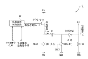
次に、図2に基づき、チャージ・ポンプ回路2の詳細な構成を説明する。
ここで、図2は、チャージ・ポンプ回路2の詳細な構成を示す回路図である。
本実施の形態のチャージ・ポンプ回路2は、図2に示すように、Pチャンネル型のMOSトランジスタであるPTr3と、キャパシタC1,C2と、スイッチング素子SW1,SW2,SW3と、供給電流制御回路20とを含んで構成される。Next, a detailed configuration of the
Here, FIG. 2 is a circuit diagram showing a detailed configuration of the
As shown in FIG. 2, the
本実施の形態において、スイッチング素子SW1,SW2及びSW3は、Nチャンネル型のMOSトランジスタから構成されている。なお、Nチャンネル型のMOSトランジスタに限らずPチャンネル型のMOSトランジスタで構成することも可能である。
供給電流制御回路20の制御信号出力端子(不図示)は、PTr3のゲート端子に電気的に接続され、PTr3のソース端子は、電源VCCの入力端子に電気的に接続されている。なお、この入力端子には、電圧VCCの電源の電源供給端子が電気的に接続されている。In the present embodiment, the switching elements SW1, SW2, and SW3 are composed of N-channel MOS transistors. It should be noted that the present invention is not limited to the N channel type MOS transistor, and may be composed of a P channel type MOS transistor.
The control signal output terminal (not shown) of the supply
PTr3のドレイン端子は、C1の正極側の端子とSW1のドレイン端子とにそれぞれ電気的に接続されており、SW1のソース端子はグランド端子(GND)に電気的に接続されている。なお、このグランド端子には、グランド電位(0[V])が接続されている。
更に、図示していないが、SW1のゲート端子は、クロック発生回路4のCLK1の出力端子と電気的に接続されている。The drain terminal of PTr3 is electrically connected to the positive terminal of C1 and the drain terminal of SW1, and the source terminal of SW1 is electrically connected to the ground terminal (GND). Note that a ground potential (0 [V]) is connected to the ground terminal.
Further, although not shown, the gate terminal of SW1 is electrically connected to the output terminal of CLK1 of the clock generation circuit 4.
C1の負極側の端子は、SW2及びSW3のドレイン端子にそれぞれ電気的に接続され、SW2のソース端子はグランド端子に電気的に接続され、SW3のソース端子はC2の負極側の端子に電気的に接続されている。
更に、図示していないが、SW2のゲート端子は、クロック発生回路4のクロック信号CLK1の出力端子と電気的に接続され、SW3のゲート端子は、クロック発生回路4のCLK2の出力端子と電気的に接続されている。The negative terminal of C1 is electrically connected to the drain terminals of SW2 and SW3, the source terminal of SW2 is electrically connected to the ground terminal, and the source terminal of SW3 is electrically connected to the negative terminal of C2. It is connected to the.
Further, although not shown, the gate terminal of SW2 is electrically connected to the output terminal of the clock signal CLK1 of the clock generation circuit 4, and the gate terminal of SW3 is electrically connected to the output terminal of CLK2 of the clock generation circuit 4. It is connected to the.
次に、図3に基づき、供給電流制御回路20の詳細な構成を説明する。
ここで、図3は、供給電流制御回路20の詳細な構成を示す回路図である。
本実施の形態の供給電流制御回路20は、図3に示すように、Pチャンネル型のMOSトランジスタであるPTr4と、スイッチング素子SW4と、Nチャンネル型のMOSトランジスタであるNTr6とを含んで構成される。
本実施の形態において、スイッチング素子SW4は、Nチャンネル型のMOSトランジスタから構成されている。なお、Nチャンネル型のMOSトランジスタに限らずPチャンネル型のMOSトランジスタで構成することも可能である。Next, a detailed configuration of the supply
Here, FIG. 3 is a circuit diagram showing a detailed configuration of the supply
As shown in FIG. 3, the supply
In the present embodiment, the switching element SW4 is composed of an N channel type MOS transistor. It should be noted that the present invention is not limited to the N channel type MOS transistor, and may be composed of a P channel type MOS transistor.
PTr4のソース端子は、電源VCCの入力端子に電気的に接続されており、ドレイン端子は、SW4のドレイン端子にそれぞれ電気的に接続されている。なお、この入力端子には、電源VCCの電源供給端子が電気的に接続されている。
PTr4のゲート端子は、PTr4のドレイン端子及びPTr3のゲート端子とそれぞれ電気的に接続されており、PTr3とPTr4とでカレントミラー回路を構成している。The source terminal of PTr4 is electrically connected to the input terminal of the power supply V CC , and the drain terminal is electrically connected to the drain terminal of SW4. Note that a power supply terminal of the power supply V CC is electrically connected to this input terminal.
The gate terminal of PTr4 is electrically connected to the drain terminal of PTr4 and the gate terminal of PTr3, respectively, and PTr3 and PTr4 constitute a current mirror circuit.
SW4のソース端子は、NTr6のドレイン端子に電気的に接続され、ゲート端子は、クロック発振回路4のCLK1の出力端子と電気的に接続されている。
NTr6のソース端子は、出力電源である負電圧VEEに電気的に接続されており、ゲート端子は、アンプ回路6を構成するNチャンネル型のMOSトランジスタであるNTr5(後述)のゲート端子と電気的に接続されている。
そして、NTr6及びSW4がオンのときに、NTr6のドレイン−ソース間を流れる電流信号である負荷電流連動信号65が、SW4を介してPTr4のゲート端子及びドレイン端子と、PTr3のゲート端子とに供給される。The source terminal of SW4 is electrically connected to the drain terminal of NTr6, and the gate terminal is electrically connected to the output terminal of CLK1 of the clock oscillation circuit 4.
The source terminal of
When NTr6 and SW4 are on, a load current interlocking signal 65, which is a current signal flowing between the drain and source of NTr6, is supplied to the gate terminal and drain terminal of PTr4 and the gate terminal of PTr3 via SW4. Is done.
上記構成によって、チャージ・ポンプ回路2は、クロック発生回路4からのCLK1がハイレベルのときにSW2及びSW4がオンになり、ローレベルのときにオフとなる。また、クロック信号CLK2がハイレベルのときにSW1及びSW3がオンになり、ローレベルのときにオフとなる。但し、SW2とSW3は負電圧領域でパスをオン・オフするために適切にレベルシフトされて用いられる。
With the above configuration, the
そして、SW2及びSW4がオンで、SW1及びSW3がオフのときに、制御信号Ctrl1がPTr3の駆動電位(PTr3をオンにする電位)のときは、PTr3がオンとなって、電源VCCからの供給電流ISUPがC1に供給され、この第1の期間(Φ1)においてC1が充電される。
また、SW2及びSW4がオフで、SW1及びSW3がオンのときは、PTr3がオフとなって、電源VCCからの供給電流がC1に供給されなくなり、この第2の期間(Φ2)においてはC1が充電されない。When SW2 and SW4 are on, SW1 and SW3 are off, and the control signal Ctrl1 is the drive potential of PTr3 (potential for turning on PTr3), PTr3 is on and the power supply V CC The supply current I SUP is supplied to C1, and C1 is charged in the first period (Φ1).
Also, when SW2 and SW4 are off and SW1 and SW3 are on, PTr3 is off and the supply current from the power supply V CC is not supplied to C1, and during this second period (Φ2), C1 Is not charged.
一方、SW2及びSW4がオフで、SW1及びSW3がオンのときは、GND−SW1−C1−SW3−C2−GNDの閉ループが構成され、C1に蓄積された電荷が、図2に示す極性でC2へと転送される。
SW2及びSW4のオン・オフと、SW1及びSW3のオン・オフとの切り替えを、上記のCLK1及びCLK2による切り替えタイミングで繰り返し(継続して)行うことで、グランド端子と出力電源の供給端子との間に、正電圧VCCの極性を反転させた電圧と略同じレベルの負電圧VEEを発生させることができる。On the other hand, when SW2 and SW4 are off and SW1 and SW3 are on, a closed loop of GND-SW1-C1-SW3-C2-GND is formed, and the charge accumulated in C1 has the polarity shown in FIG. Forwarded to
By repeatedly (continuously) switching on / off of SW2 and SW4 and on / off of SW1 and SW3 at the switching timing according to the above-described CLK1 and CLK2, the ground terminal and the output power supply terminal In the meantime , it is possible to generate the negative voltage V EE having substantially the same level as the voltage obtained by inverting the polarity of the positive voltage V CC .
また、制御信号Ctrl1の電位は、負荷電流連動信号65の電流レベルに応じて変化し、負荷電流連動信号65の電流レベルが大きければ大きいほど制御信号Ctrl1の電位が低くなる。従って、負荷電流連動信号65の電流レベルが大きければ大きいほどPTr3のゲート−ソース間の電圧VGSが負方向に大きくなり、これにより、供給電流ISUPが大きくなる。
つまり、負荷電流連動信号65と、供給電流ISUPとの間には正の相関が成立し、負荷電流連動信号65の電流レベルの増減に応じて、キャパシタC1への供給電流量が増減する。Further, the potential of the control signal Ctrl1 changes according to the current level of the load current interlocking signal 65, and the potential of the control signal Ctrl1 decreases as the current level of the load current interlocking signal 65 increases. Therefore, the gate of the larger the PTr3 larger the current level of the load current interlock signal 65 - the voltage V GS between source is increased in the negative direction, thereby, the supply current I SUP is increased.
That is, a positive correlation is established between the load current interlocking signal 65 and the supply current ISUP, and the amount of supply current to the capacitor C1 increases or decreases according to the increase or decrease of the current level of the load current interlocking signal 65.
次に、図4に基づき、アンプ回路6の詳細な構成を説明する。
ここで、図4は、アンプ回路6の詳細な構成を示す回路図である。
アンプ回路6は、図4に示すように、入力段差動回路60と、出力段回路62と、抵抗Rs,Rfとを含んで構成される。
入力段差動回路60は、負荷Aと、負荷Bと、Nチャンネル型のMOSトランジスタであるNTr1,NTr2,NTr3とを含んで構成される。
出力段回路62は、Pチャンネル型のMOSトランジスタであるPTr1,PTr2、Nチャンネル型のMOSトランジスタであるNTr4,NTr5と、位相補償のための抵抗R10及びキャパシタC10とを含んで構成される。Next, a detailed configuration of the
Here, FIG. 4 is a circuit diagram showing a detailed configuration of the
As shown in FIG. 4, the
The input stage
The
抵抗Rs,Rfは、アンプ回路6の電圧利得を決めると共に出力信号Soutを反転入力端子(−)であるNTr2のゲート端子に帰還させる役割を有している。
つまり、アンプ回路6は、差動対となる入力段差動回路60と出力段回路62とから構成されるOPアンプと、抵抗Rs及びRfとを含んで構成される反転増幅回路となる。
本実施の形態において、負荷A及び負荷Bは、抵抗素子RA及びRBとする。なお、負荷A及び負荷Bは、MOSトランジスタを用いたカレントミラー回路として構成するなど、他の素子を用いて構成してもよい。The resistors R s and R f determine the voltage gain of the
That is, the
In this embodiment, the load A and the load B is a resistive element R A and R B. The load A and the load B may be configured using other elements such as a current mirror circuit using a MOS transistor.
また、アンプ回路6の正電源入力端子及び負電源入力端子には、チャージ・ポンプ回路2から、正電圧VCCの正電源と、負電圧VEEの負電源とが供給されている。
入力段差動回路60を構成する、RA及びRBの一端は、電源VCCの正電源入力端子にそれぞれ電気的に接続され、RAの他端は、NTr1のドレイン端子に電気的に接続され、RBの他端は、NTr2のドレイン端子に電気的に接続されている。Further, the positive power source input terminal and the negative power source input terminal of the
One end of R A and R B constituting the input stage
更に、NTr1及びNTr2のソース端子は、NTr3のドレイン端子に電気的に接続され、NTr3のソース端子は、電源VEEの負電源入力端子に電気的に接続されている。
更に、NTr2のゲート端子は、入力信号Sinの入力端子になっており、外部の装置(不図示)から入力信号Sinが入力される。
更に、NTr1のゲート端子は、レベル調整電圧Vrが印加され、NTr3のゲート端子には、NTr3を飽和領域で駆動させるのに十分な定電流生成電圧Vbが印加される。Further, the source terminal of NTr1 and NTr2 is electrically connected to the drain terminal of NTr3, the source terminal of NTr3 is electrically connected to the negative power supply input terminal of the power source V EE.
Furthermore, the gate terminal of NTr2 is adapted to the input terminal of the input signal S in, the input signal S in is input from an external device (not shown).
Furthermore, a level adjustment voltage Vr is applied to the gate terminal of NTr1, and a constant current generation voltage Vb sufficient to drive NTr3 in the saturation region is applied to the gate terminal of NTr3.
出力段回路62を構成する、PTr1、PTr2のソース端子は、正電源入力端子に電気的に接続され、PTr1のゲート端子は、NTr2のドレイン端子に電気的に接続されており、PTr2のゲート端子には、PTr2を飽和領域で駆動させるのに十分な定電流生成電圧Vb2が印加される。
更に、PTr1のドレイン端子は、NTr4のドレイン端子と電気的に接続され、PTr2のドレイン端子は、NTr5のドレイン端子と電気的に接続され、NTr4及びNTr5のソース端子は、負電源入力端子と電気的に接続されている。The source terminals of PTr1 and PTr2 constituting the
Furthermore, the drain terminal of PTr1 is electrically connected to the drain terminal of NTr4, the drain terminal of PTr2 is electrically connected to the drain terminal of NTr5, and the source terminals of NTr4 and NTr5 are electrically connected to the negative power supply input terminal. Connected.
更に、NTr5のゲート端子は、抵抗R10の一端と電気的に接続され、R10の他端はキャパシタC10の一端と電気的に接続され、C10の他端はNTr5のドレイン端子及び信号出力端子にそれぞれ電気的に接続されている。また、信号出力端子は、負荷8と電気的に接続されている。
更に、NTr4のゲート端子とNTr5のゲート端子とは電気的に接続されており、NTr4のゲート端子とドレイン端子とは電気的に接続されている。この構成により、NTr4とNTr5とカレントミラー回路を構成する。Furthermore, the gate terminal of NTr5 has one end and is electrically connected to resistors R 10, the other end of R 10 are electrically connected to one end of the capacitor C 10, a drain terminal and a signal at the other end to C 10 are NTr5 Each output terminal is electrically connected. The signal output terminal is electrically connected to the
Furthermore, the gate terminal of NTr4 and the gate terminal of NTr5 are electrically connected, and the gate terminal and drain terminal of NTr4 are electrically connected. With this configuration, NTr4 and NTr5 constitute a current mirror circuit.
また、NTr4及びNTr5のゲート端子は、NTr6のゲート端子と電気的に接続されており、NTr5のドレイン−ソース間を流れる第1の電流と、NTr6のドレイン−ソース間を流れる第2の電流との間にカレントミラーの関係が成立している。なお、第1の電流は、負荷8に流れる電流ILであり、第2の電流は、負荷電流ILに比例した電流となり、この電流信号が負荷電流連動信号65である。つまり、負荷電流連動信号65は、NTr5とNTr6とのサイズの比(チャンネル幅及びチャンネル長の比)によって決まる。双方ともサイズが同じであれば、負荷電流連動信号65は、負荷電流ILと略同じレベルの電流信号となる。The gate terminals of NTr4 and NTr5 are electrically connected to the gate terminal of NTr6, and a first current that flows between the drain and source of NTr5, and a second current that flows between the drain and source of NTr6, Current mirror relationship is established between the two. The first current is a current I L flowing through the
また、抵抗Rsの一端は信号入力端子と電気的に接続され、他端は、抵抗Rfの一端及びNTr2のゲート端子とそれぞれ電気的に接続され、Rfの他端は、信号出力端子と電気的に接続されている。
上記構成のアンプ回路6は、チャージ・ポンプ回路2で生成されると共に同回路2から供給される負電圧VEEの負電源と、正電圧VCCの正電源とによって駆動され、入力信号Sinを、抵抗Rs、Rfによって決まる増幅度でレベル調整電圧Vrを中心に反転増幅し、グランド電圧(0[V])中心の出力信号Soutとして出力する。One end of the resistor R s is electrically connected to the signal input terminal, the other end is electrically connected to one end of the resistor R f and the gate terminal of NTr2, and the other end of R f is the signal output terminal. And are electrically connected.
The
また、出力段回路62は相補型のPTr2とNTr5とから最終出力段が構成され、それぞれVb2及びNTr4からの信号が与えられ制御される。
この構成によって、出力信号Soutはグランド電圧の上下の電圧範囲にわたって出力される。
本実施の形態において、上記説明したチャージ・ポンプ回路2及びアンプ回路6のうち少なくともチャージ・ポンプ回路2は、半導体基板上にMOSトランジスタを用いて集積された半導体集積回路として構成される。Further, the
With this configuration, the output signal Sout is output over a voltage range above and below the ground voltage.
In the present embodiment, at least the
次に、図5に基づき、本実施の形態の負荷駆動システム1のより具体的な動作を説明する。
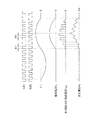
ここで、図5は、チャージ・ポンプ回路2、クロック発生回路4及びアンプ回路6を流れる信号のタイミングチャートである。
図5において、クロック信号CLK1,CLK2、入力信号Sinは電圧波形であり、負電圧VEEの電源の供給端子に流れ込む負荷電流ILは、電流の絶対値の波形である。また、発生電圧VGは、負電圧VEE(定電圧)を基準としたときに発生する電圧である。
負荷駆動システム1の各回路に電源を供給すると、各回路が起動し、図5に示すタイミングで、クロック信号CLK1がSW2及びSW4のゲート端子に供給され、クロック信号CLK2がSW1及びSW3のゲート端子に供給され、入力信号Sinがアンプ回路6の反転入力端子(−)に入力される。Next, a more specific operation of the
Here, FIG. 5 is a timing chart of signals flowing through the
5, the clock signal CLK1, CLK2, the input signal S in is a voltage waveform, the load current I L flowing into the power supply terminal of the negative voltage V EE is a waveform of the absolute value of the current. The generated voltage V G is a voltage generated when the negative voltage V EE (constant voltage) is used as a reference.
When power is supplied to each circuit of the
これにより、入力信号Sinが負電圧の期間において、CLK1がハイレベルの期間(Φ1)は、CLK2がローレベルとなり、チャージ・ポンプ回路2のSW2及びSW4がオン、SW1及びSW3がオフ、PTr4がオンとなる。しかし、入力信号Sinが負電圧であるため、正電圧VCCの電源から負荷8に電流が供給され、負電圧VEEの電源からは負荷8に負荷電流ILが供給されない。そのため、制御信号Ctrl1の電位がVCCと略同じ電位となり、PTr3がオフとなる。従って、C1には供給電流ISUPが供給されないため、C1は充電されない。As a result, during the period when the input signal S in is a negative voltage, the period CLK1 is high (Φ1), the period CLK2 is low, SW2 and SW4 of the
引き続き、CLK2がハイレベルの期間(Φ2)は、CLK1がローレベルになり、チャージ・ポンプ回路2のSW2及びSW4がオフ、且つSW1及びSW3がオンとなる。しかし、入力信号Sinが負電圧の期間は、Φ1の期間にC1に供給電流ISUPが供給されないため、C1からC2への電荷の転送が行われない。また、PTr3及びPTr4もオフとなる。
以上より、入力信号Sinが負電圧の期間は、図5に示すように、負荷電流IL、供給電流ISUP及び、電圧VEEを基準とした発生電圧VGはいずれも「0」となる。Subsequently, during a period (Φ2) when CLK2 is at a high level, CLK1 is at a low level, SW2 and SW4 of the
From the above, during the period in which the input signal S in is a negative voltage, as shown in FIG. 5, the load voltage I L , the supply current I SUP, and the generated voltage V G based on the voltage V EE are all “0”. Become.
一方、入力信号Sinが正電圧の期間において、CLK1がハイレベルの期間(Φ1)は、CLK2がローレベルとなり、チャージ・ポンプ回路2のSW2及びSW4がオン、SW1及びSW3がオフとなる。入力信号Sinが正電圧のときは、負電圧VEEの電源から負荷8に負荷電流ILが供給される。このとき、チャージ・ポンプ回路2の供給電流制御回路20のNTr6もオンとなる。On the other hand, during a period when the input signal S in is a positive voltage and the CLK1 is at a high level (Φ1), CLK2 is at a low level, SW2 and SW4 of the
従って、負荷電流ILに比例した負荷電流連動信号65が、NTr6のドレイン−ソース間を流れる。また、Φ1の期間は、SW4がオンとなり、負荷電流連動信号65がPTr4及びPTr3のゲート端子に供給され、制御信号Ctrl1の電位が負荷電流連動信号65の電流レベルに応じた電位(低電位)となり、PTr3のVGSが駆動電位となってPTr3がオンとなる。これにより、Φ1の期間において、図5に示すように、負荷電流ILの電流レベルに比例した供給電流ISUPがC1に供給され、C1が充電される。Therefore, the load current interlock signal 65 which is proportional to the load current I L, the drain of NTr6 - flowing between the source. During the period Φ1, SW4 is turned on, the load current interlocking signal 65 is supplied to the gate terminals of PTr4 and PTr3, and the potential of the control signal Ctrl1 is a potential (low potential) corresponding to the current level of the load current interlocking signal 65. next, PTr3 is on V GS of PTr3 becomes the driving potential. Thus, in the period of .phi.1, as shown in FIG. 5, is supplied to the load current supply current I SUP is C1 proportional to the current level of I L, C1 is charged.
引き続き、CLK2がハイレベルの期間(Φ2)は、CLK1がローレベルになり、チャージ・ポンプ回路2のSW2及びSW4がオフ、且つSW1及びSW3がオン、PTr3及びPTr4がオフとなる。これによって、Φ1の期間にC1に蓄積された電荷がC2に転送され、C2が充電される。更に、負電圧VEEの電源から負荷8に負荷電流ILが供給される。Subsequently, during a period (Φ2) when CLK2 is at a high level, CLK1 is at a low level, SW2 and SW4 of the
以上より、入力信号Sinが正電圧の期間は、図5に示すように、供給電流ISUPは、負荷電流ILのレベルに応じた出力値となり、発生電圧VGは、供給電流ISUPのレベル(供給量)に応じた出力値となる。
具体的に、発生電圧VGは、Φ1の期間では負荷電流ILによって、グランド方向に上昇するが、Φ2の期間でキャパシタC1に蓄えられた電荷が転送されて負電圧方向に下降する。このとき、転送される電荷量は、Φ1の期間にキャパシタC1に蓄積される電荷量(供給電流ISUP)と正の相関がある。Thus, the period of the input signal S in a positive voltage, as shown in FIG. 5, the supply current I SUP, the output value becomes corresponding to the level of the load current I L, the generated voltage V G, the supply current I SUP It becomes an output value according to the level (supply amount).
Specifically, the generated voltage V G rises in the ground direction due to the load current I L during the period Φ1, but drops in the negative voltage direction due to transfer of the charge stored in the capacitor C1 during the period Φ2. At this time, the transferred charge amount has a positive correlation with the charge amount (supply current I SUP ) accumulated in the capacitor C1 during the period Φ1.
また、Φ1とΦ2の期間が交互に繰り返されることで発生電圧VGが生じて、負電圧VEEは上昇と下降がバランスする電圧領域で微小な上下を繰り返す。しかし、負電圧VEEの微小な上下は、チャージ・ポンプ回路2に適切に大きな容量値のキャパシタC1、C2(この容量値は駆動する負荷の大きさ等に依存して決まり、一般に、0.01[μF]〜100[μF]で、好ましくは1[μF]となる)を用いることで吸収することができる。これによって、負電圧VEEとして、正電圧VCCと絶対値が同じ負の電圧に十分近い電圧を作ることができる。このようにして生成した負電圧VEEによって、アンプ回路6は、入力信号Sinの正電圧部分の信号を適切に増幅することができると共に、負荷8を十分に駆動できるものとなる。Further, the generated voltage V G is generated by alternately repeating the periods of
以上、本実施の形態のチャージ・ポンプ回路2は、アンプ回路6のNTr5とカレントミラーの関係にあるNTr6によって、負荷電流ILに比例したレベルの電流を流す負荷電流連動信号65を生成して、PTr3のソース−ドレイン間に流れる電流(供給電流ISUP)を制御し、図6に示すように負荷電流ILと供給電流ISUPに正の相関を持たせることで、Φ2の期間にキャパシタC1から転送される電荷量と負荷電流ILの間に正の相関を生じさせることができる。Above, the
ここで、図6は、負荷電流ILと供給電流ISUPとの関係を示す図である。
これにより、負電圧VEEの電源供給端子に流れ込む負荷電流ILを効率よく転送させることができると共に、アンプ回路6の動作条件に応じた供給電流ISUPをキャパシタC1に供給することが可能になり、通常使用範囲において発生する電源ノイズを小さくすることができる。
上記第1の実施の形態において、供給電流制御回路20は、発明1、2、6及び8のいずれか1に記載の供給電流量制御手段に対応する。Here, FIG. 6 is a diagram showing the relationship between the load current I L and the supply current I SUP .
As a result, the load current I L flowing into the power supply terminal of the negative voltage V EE can be efficiently transferred, and the supply current I SUP corresponding to the operating condition of the
In the first embodiment, the supply
〔第2の実施の形態〕
次に、本発明の第2の実施の形態を図面に基づき説明する。図7〜図9は、本発明に係るチャージ・ポンプ回路及び半導体集積回路の第2の実施の形態を示す図である。
上記第1の実施の形態のチャージ・ポンプ回路2は、キャパシタC1を充電して、正電圧VCCと絶対値が略同じ負電圧VEEを生成していたが、これに対して、本実施の形態のチャージ・ポンプ回路3は、キャパシタC1の両端の電圧を監視し、所定の電圧に到達したときにC1への電荷の蓄積を終了させることができる点が上記第1の実施の形態のチャージ・ポンプ回路2と異なる。[Second Embodiment]
Next, a second embodiment of the present invention will be described with reference to the drawings. FIGS. 7 to 9 are diagrams showing a second embodiment of the charge pump circuit and the semiconductor integrated circuit according to the present invention.
The
従って、チャージ・ポンプ回路以外の他の構成部は、上記第1の実施の形態と同様となる。以下、上記第1の実施の形態のチャージ・ポンプ回路2と異なる部分を詳細に説明し、同様の部分は同じ符号を付して説明を適宜省略する。
まず、図7に基づき、本実施の形態のチャージ・ポンプ回路3の詳細な構成を説明する。
ここで、図7は、チャージ・ポンプ回路3の詳細な構成を示す回路図である。
本実施の形態のチャージ・ポンプ回路3は、図7に示すように、Pチャンネル型のMOSトランジスタであるPTr3と、キャパシタC1,C2と、スイッチング素子SW1,SW2,SW3と、供給電流制御回路21と、電圧モニター回路22とを含んで構成される。Therefore, other components than the charge pump circuit are the same as those in the first embodiment. Hereinafter, parts different from the
First, based on FIG. 7, the detailed structure of the charge pump circuit 3 of this Embodiment is demonstrated.
Here, FIG. 7 is a circuit diagram showing a detailed configuration of the charge pump circuit 3.
As shown in FIG. 7, the charge pump circuit 3 of the present embodiment includes a PTr3 that is a P-channel MOS transistor, capacitors C1 and C2, switching elements SW1, SW2, and SW3, and a supply
供給電流制御回路21の制御信号出力端子(不図示)は、PTr3のゲート端子に電気的に接続され、PTr3のソース端子は、電源VCCの入力端子に電気的に接続されている。なお、この入力端子には、電圧VCCの電源の電源供給端子が電気的に接続されている。
電圧モニター回路22の、正電圧監視用端子はC1の正極側の端子に電気的に接続され、負電圧監視用端子はC1の負極側の端子に電気的に接続され、制御信号出力端子は供給電流制御回路21の制御信号入力端子と電気的に接続されている。
他の接続構成は、上記第1の実施の形態のチャージ・ポンプ回路2と同様となる。The control signal output terminal (not shown) of the supply
The positive voltage monitoring terminal of the
Other connection configurations are the same as those of the
次に、図8に基づき、供給電流制御回路21の詳細な構成を説明する。
ここで、図8は、供給電流制御回路21の詳細な構成を示す回路図である。
本実施の形態の供給電流制御回路21は、図8に示すように、Pチャンネル型のMOSトランジスタであるPTr4と、スイッチング素子SW4と、Nチャンネル型のMOSトランジスタであるNTr6と、NOT回路23と、AND回路24とを含んで構成される。Next, a detailed configuration of the supply
Here, FIG. 8 is a circuit diagram showing a detailed configuration of the supply
As shown in FIG. 8, the supply
SW4のゲート端子は、AND回路24の出力端子に電気的に接続され、AND回路24の第1の入力端子は、NOT回路23の出力端子に電気的に接続され、AND回路24の第2の入力端子は、クロック発振回路4のCLK1の出力端子と電気的に接続されている。
更に、NOT回路23の入力端子(制御信号入力端子)は、電圧モニター回路22の制御信号出力端子と電気的に接続されている。
なお、他の接続構成は、上記第1の実施の形態の供給電流制御回路20と同様となる。The gate terminal of SW4 is electrically connected to the output terminal of the AND
Further, the input terminal (control signal input terminal) of the
The other connection configuration is the same as that of the supply
次に、図9に基づき、電圧モニター回路22の詳細な構成を説明する。
ここで、図9は、電圧モニター回路22の詳細な構成を示す回路図である。
電圧モニター回路22は、図9に示すように、減算回路25と、コンパレータ回路26とを含んで構成される。
減算回路25は、上記した正電圧監視用端子、上記した負電圧監視用端子及び減算結果出力端子を備え、減算結果出力端子は、コンパレータ回路26の比較電圧入力端子と電気的に接続されている。
更に、減算回路25は、正電圧監視用端子に入力される正側電圧V+から、負電圧監視用端子に入力される負側電圧V-を減算し、減算結果に応じた電圧Vdを減算結果出力端子から出力する。Next, a detailed configuration of the
Here, FIG. 9 is a circuit diagram showing a detailed configuration of the
As shown in FIG. 9, the
The
Further, the subtracting
コンパレータ回路26は、比較電圧入力端子、参照電圧入力端子及び上記した制御信号出力端子を備え、比較電圧入力端子に入力される電圧Vdと、参照電圧入力端子に入力される参照電圧Vref(Vref<VCC)とを比較し、VdがVref未満のときは制御信号出力端子からローレベルの電流制御信号CCtrl1を出力し、VdがVref以上のときは制御信号出力端子からハイレベルの電流制御信号CCtrl1を出力する。The
上記構成によって、チャージ・ポンプ回路3は、クロック発生回路4からのCLK1がハイレベルで且つ電流制御信号CCtrl1がローレベルのときに、SW2及びSW4がオンになり、CLK1がローレベル又はCCtrl1がハイレベルのときにオフとなる。
つまり、C1の両端間電圧Vdが参照電圧Vref未満のときは、電流制御信号CCtrl1がローレベルになり、AND回路24の第1の入力端子にはNOT回路23でハイレベルへと反転されたCCtrl1が入力され、AND回路24の出力は、CLK1がハイレベルのときにハイレベルとなる。With the above configuration, when the CLK1 from the clock generation circuit 4 is at a high level and the current control signal CCtrl1 is at a low level, the charge pump circuit 3 turns on SW2 and SW4, and CLK1 is at a low level or CCtrl1 is at a high level. Off when level.
That is, when the voltage V d between both ends of C1 is less than the reference voltage Vref, the current control signal CCtrl1 becomes low level, and the first input terminal of the AND
一方、C1の両端間電圧Vdが参照電圧Vref以上のときは、電流制御信号CCtrl1がハイレベルとなり、AND回路24の第1の入力端子にはNOT回路23でローレベルへと反転されたCCtrl1が入力され、AND回路24の出力は、CLK1がハイレベル又はローレベルのいずれであってもローレベルとなる。
いま、CLK1がハイレベルで且つCCtrl1がローレベルになってSW2及びSW4がオンになり、CLK2がローレベルになってSW1及びSW3がオフになると、PTr3がオンとなる。これによって、電源VCCからの負荷電流ILと正の相関にある供給電流ISUPがC1に供給されC1の充電が開始される。On the other hand, when the voltage V d between both ends of C1 is equal to or higher than the reference voltage Vref, the current control signal CCtrl1 is at a high level, and the first input terminal of the AND
Now, when CLK1 is at a high level and CCtrl1 is at a low level and SW2 and SW4 are turned on, and when CLK2 is at a low level and SW1 and SW3 are turned off, PTr3 is turned on. As a result, the supply current I SUP having a positive correlation with the load current I L from the power source V CC is supplied to C1, and charging of C1 is started.
一方、C1が充電中において(CLK1がハイレベルであるΦ1の期間において)CCtrl1がハイレベルになると、SW4がオフとなって、PTr3及びPTr4もオフとなり、C1の充電は強制的に終了される。これによって、C1の両端間電圧を略Vrefとすることができる。
引き続き、CLK1がローレベルになってSW2及びSW4がオフになり、CLK2がハイレベルになってSW1及びSW3がオンになると、GND−SW1−C1−SW3−C2−GNDのループが構成され、C1に蓄積された電荷が、図7に示す極性でC2へと転送される。これにより、供給端子のVEEの電圧レベルをVrefのレベルとすることができる。
なお、その他の動作については、上記第1の実施の形態のチャージ・ポンプ回路2と同様となる。On the other hand, when CCtrl1 goes high while C1 is charging (during the period of Φ1 when CLK1 is high), SW4 is turned off, PTr3 and PTr4 are also turned off, and charging of C1 is forcibly terminated. . As a result, the voltage across C1 can be made substantially Vref.
Subsequently, when CLK1 becomes low level and SW2 and SW4 are turned off, and CLK2 becomes high level and SW1 and SW3 are turned on, a loop of GND-SW1-C1-SW3-C2-GND is formed, and C1 Is transferred to C2 with the polarity shown in FIG. This makes it possible to the voltage level of V EE supply terminal and the level of Vref.
Other operations are the same as those of the
以上、本実施の形態の負荷駆動システム1は、供給電流制御回路21によって、アンプ回路6を流れる負荷電流ILと正の相関を持った供給電流ISUPによって、チャージ・ポンプ回路3のC1を充電することができる。
更に、電圧モニター回路22によって、C1の両端の電圧を監視し、両端間の電圧がVref以上になったときに、供給電流制御回路21によって、SW4をオフにしC1への充電をVCCよりも小さいVrefで終了させることができる。
つまり、Vrefを所望の電圧とすることで、VEEをVCCよりも低い所望の電圧にすることができる。Above, the
Further, the
That is, by the Vref and desired voltage, it is possible to the V EE to a desired voltage lower than V CC.
従来のチャージ・ポンプ回路を用いてこのような構成にした場合、キャパシタC1の充電が不十分の状態で電荷の蓄積を終了させるため、供給電流が非常に大きくなってしまう。一方、本実施の形態のチャージ・ポンプ回路3では、アンプ回路6の動作条件に応じた供給電流ISUPをキャパシタC1に供給することが可能になり、Vrefの段階でC1の充電を終了する使い方をしても、そのときに発生する電源ノイズを小さくすることができる。In the case of such a configuration using a conventional charge pump circuit, since the charge accumulation is terminated in a state where the capacitor C1 is not sufficiently charged, the supply current becomes very large. On the other hand, in the charge pump circuit 3 according to the present embodiment, it becomes possible to supply the supply current ISUP corresponding to the operating condition of the
上記第2の実施の形態において、供給電流制御回路21は、発明1、2、6及び8のいずれか1に記載の供給電流量制御手段に対応し、電圧モニター回路22は、発明4に記載の電圧レベル比較手段に対応し、供給電流制御回路21における電圧モニター回路22からの電流制御信号CCtrl1に基づきSW4を切り替える処理は、発明4に記載の切替制御手段に対応する。
In the second embodiment, the supply
〔第3の実施の形態〕
次に、本発明の第3の実施の形態を図面に基づき説明する。図10は、本発明に係るチャージ・ポンプ回路及び半導体集積回路の第3の実施の形態を示す図である。
上記第1の実施の形態の負荷駆動システム1は、チャージ・ポンプ回路2の被駆動回路として、1つのアンプ回路6を駆動する構成にしていたが、本実施の形態の負荷駆動システム10は、チャージ・ポンプ回路2の被駆動回路として、2つのアンプ回路6A及び6Bを駆動する点が上記第1の実施の形態と異なる。[Third Embodiment]
Next, a third embodiment of the present invention will be described with reference to the drawings. FIG. 10 is a diagram showing a third embodiment of the charge pump circuit and the semiconductor integrated circuit according to the present invention.
The
更に、本実施の形態の負荷駆動システム10は、キャパシタC1の充電を行うときに、アンプ回路6Aに流れる負荷電流ILAと正の相関を有する負荷電流連動信号65Aと、アンプ回路6Bに流れる負荷電流ILBと正の相関を有する負荷電流連動信号65Bとの和からなる負荷電流連動信号65Cと正の相関を有する(比例する)供給電流ISUPによって、C1を充電する点が上記第1の実施の形態と異なる。
従って、アンプ回路6が、アンプ回路6A及び6Bになる点と、負荷電流連動信号65A及び65Bの和をSW4を介してPTr3及びPTr4に供給する点以外の他の構成部は、上記第1の実施の形態と同様となる。以下、上記第1の実施の形態と異なる部分を詳細に説明し、同様の部分は同じ符号を付して説明を適宜省略する。Furthermore, the
Therefore, the components other than the point where the
図10に基づき、本実施の形態の負荷駆動システム10の構成を説明する。
ここで、図10は、負荷駆動システム10の構成を示すブロック図である。
負荷駆動システム10は、図10に示すように、チャージ・ポンプ回路2と、クロック発生回路4と、アンプ回路6A及び6Bと、負荷8A及び8Bとを含んで構成される。
アンプ回路6Aからは、上記第1の実施の形態のNTr6と同様の役割を果たすNTr6Aを介して、アンプ回路6Aを流れる負荷電流ILAと正の相関を有する負荷電流連動信号65Aを伝送する導電性のラインL1がチャージ・ポンプ回路2に向けて伸びている。Based on FIG. 10, the structure of the
Here, FIG. 10 is a block diagram showing a configuration of the
As shown in FIG. 10, the
From the
また、アンプ回路6Bからは、上記第1の実施の形態のNTr6と同様の役割を果たす、NTr6Bを介して、アンプ回路6Bを流れる負荷電流ILBと正の相関を有する負荷電流連動信号65Bを伝送する導電性のラインL2がチャージ・ポンプ回路2に向けて伸びている。
従って、本実施の形態では、NTr6Aは、アンプ回路6A側に設け、NTr6Bはアンプ回路6B側に設けている。なお、NTr6A及び6Bを、チャージ・ポンプ回路2側に設ける構成としてもよい。Also, from the
Therefore, in the present embodiment, NTr6A is provided on the
そして、ラインL1とL2とはチャージ・ポンプ回路2の手前で合流してラインL3となり、ラインL3がチャージ・ポンプ回路2のSW4と電気的に接続される。
これにより、ラインL1を流れる負荷電流連動信号65Aと、ラインL2を流れる負荷電流連動信号65Bとが合流してラインL3には、負荷電流連動信号65Aと負荷電流連動信号65Bとを合算した信号である負荷電流連動信号65Cが流れる。The lines L1 and L2 merge before the
As a result, the load current interlocking signal 65A flowing through the line L1 and the load current interlocking signal 65B flowing through the line L2 merge, and the line L3 is a signal obtained by adding the load current interlocking signal 65A and the load current interlocking signal 65B. A certain load current interlocking signal 65C flows.
更に、チャージ・ポンプ回路2からは、電圧VEEの電源を供給する導電性のラインL4がアンプ回路6A及び6Bに向けて伸びており、ラインL4は、途中でアンプ回路6Aに向けて伸びるラインL5とアンプ回路6Bに向けて伸びるラインL6とに分岐して、それぞれ、アンプ回路6A及び6Bの負電源供給端子に電気的に接続される。
従って、ラインL4を流れる負荷電流ILは、ラインL5を流れる負荷電流ILAと、ラインL6を流れる負荷電流ILBとを合算した電流(IL=ILA+ILB)となる。Further, a conductive line L4 for supplying power of voltage V EE extends from the
Therefore, the load current I L flowing through the line L4 is a sum of the load current I LA flowing through the line L5 and the load current I LB flowing through the line L6 (I L = I LA + I LB ).
なお、説明の便宜上、ラインという言葉を用いて説明したが、信号を伝送可能な導電性のパターンであればラインに限らない。また、同じ状態を作り出せれば、加算器を用いるなどどのような構成でもよい。
更に、負荷8Aは、アンプ回路6Aによって駆動される負荷であり、負荷8Bは、アンプ回路6Bによって駆動される負荷である。
また、アンプ回路6A及び6Bは、入力信号(SinA、SinB)及び駆動する負荷(8A、8B)が異なる(同じ内容でも良い)だけで、上記第1の実施の形態のアンプ回路6と同様の構成及び動作となる。For convenience of explanation, the term “line” is used for description, but the present invention is not limited to a line as long as it is a conductive pattern capable of transmitting a signal. Moreover, as long as the same state can be created, any configuration such as using an adder may be used.
Furthermore, the
The
また、説明の便宜上、図10に示す例では、2つのアンプ回路6A及び6Bを駆動する構成としたが、これに限らず、3つ以上のアンプ回路を駆動する構成としてもよい。また、アンプ回路に限らず、他の被駆動回路を複数駆動する構成としてもよい。また、本実施の形態の構成は、上記第2の実施の形態にも適用することが可能である。
上記構成によって、チャージ・ポンプ回路2は、Φ1の期間において、負荷電流連動信号65Cに比例する供給電流ISUPによってC1を充電することができる。Further, for convenience of explanation, in the example shown in FIG. 10, the two
The above configuration, the
以上より、本実施の形態の負荷駆動システム10は、チャージ・ポンプ回路2の被駆動回路である、アンプ回路6A及び6Bを流れる負荷電流ILA及びILBの和の電流と正の相関のある供給電流ISUPによってC1を充電することができる。
これにより、例えば、ステレオヘッドホンアンプなどの複数のアンプ回路を含むデバイスを効率よく駆動することができる。
上記第3の実施の形態において、供給電流制御回路20は、発明1、2、5、6及び8のいずれか1に記載の供給電流量制御手段に対応する。As described above, the
Thereby, for example, a device including a plurality of amplifier circuits such as a stereo headphone amplifier can be efficiently driven.
In the third embodiment, the supply
〔第4の実施の形態〕
次に、本発明の第4の実施の形態を図面に基づき説明する。図11〜図12は、本発明に係るチャージ・ポンプ回路及び半導体集積回路の第4の実施の形態を示す図である。
上記第1の実施の形態の負荷駆動システム1は、チャージ・ポンプ回路2において、アンプ回路6を流れる負荷電流ILと正の相関を持った供給電流ISUPによって、C1を充電する構成としたが、本実施の形態の負荷駆動システム11は、負荷電流ILと正の相関を持った負荷電流連動信号65に、予め設定したレベルの定電流を加算して負荷電流連動信号65Dを生成し、この信号と比例する供給電流ISUPによって、C1を充電する点が上記第1の実施の形態と異なる。
従って、負荷電流連動信号65に、予め設定したレベルの定電流を加算する定電流源を追加した以外は、上記第1の実施の形態と同様となる。以下、上記第1の実施の形態と異なる部分を詳細に説明し、同様の部分は同じ符号を付して説明を適宜省略する。[Fourth Embodiment]
Next, a fourth embodiment of the present invention will be described with reference to the drawings. 11 to 12 are diagrams showing a fourth embodiment of the charge pump circuit and the semiconductor integrated circuit according to the present invention.
Accordingly, the present embodiment is the same as the first embodiment except that a constant current source for adding a preset level of constant current is added to the load current interlocking signal 65. Hereinafter, parts different from those of the first embodiment will be described in detail, and the same parts are denoted by the same reference numerals, and description thereof will be omitted as appropriate.
図11に基づき、本実施の形態の負荷駆動システム11の構成を説明する。
ここで、図11は、負荷駆動システム11の構成を示すブロック図である。
負荷駆動システム11は、図11に示すように、チャージ・ポンプ回路2と、クロック発生回路4と、アンプ回路6と、負荷8と、定電流源12とを含んで構成される。
アンプ回路6からは、NTr6を介して、アンプ回路6を流れる負荷電流ILと正の相関を有する負荷電流連動信号65を伝送する導電性のラインL1がチャージ・ポンプ回路2に向けて伸びている。Based on FIG. 11, the structure of the
Here, FIG. 11 is a block diagram showing a configuration of the
As shown in FIG. 11, the
From the
従って、本実施の形態では、NTr6は、アンプ回路6側に設けている。なお、NTr6を、チャージ・ポンプ回路2側に設ける構成としてもよい。
定電流源12は、予め定められた電流レベルの定電流信号IAを出力する機能を有している。定電流源12からは、定電流信号IAを伝送する導電性のラインL2がチャージ・ポンプ回路2に向けて伸びている。
ラインL1とラインL2とは、チャージ・ポンプ回路2の手前で合流してラインL3となり、ラインL3がチャージ・ポンプ回路2のSW4と電気的に接続される。
これにより、ラインL1を流れる負荷電流連動信号65と、ラインL2を流れる定電流信号IAとが合流してラインL3には、負荷電流連動信号65と定電流信号IAとを合算した信号である負荷電流連動信号65Dが流れる。Therefore, in the present embodiment, NTr6 is provided on the
The constant
The line L1 and the line L2 merge before the
As a result, the load current interlocking signal 65 flowing through the line L1 and the constant current signal I A flowing through the line L2 merge, and the line L3 is a signal obtained by adding the load current interlocking signal 65 and the constant current signal I A. A certain load current interlocking signal 65D flows.
なお、説明の便宜上、ラインという言葉を用いて説明したが、信号を伝送可能な導電性のパターンであればラインに限らない。同じ状態を作り出せれば、例えば、加算器を設けるなどどのような構成でもよい。
上記構成によって、チャージ・ポンプ回路2は、Φ1の期間において、負荷電流連動信号65Dに比例する供給電流ISUPによってC1を充電することができる。For convenience of explanation, the term “line” is used for description, but the present invention is not limited to a line as long as it is a conductive pattern capable of transmitting a signal. As long as the same state can be created, for example, any configuration such as providing an adder may be used.
The above configuration, the
具体的に、上記第1の実施の形態の供給電流をISUP1とし、本実施の形態の供給電流をISUP2とし、定電流信号IAの上乗せ分をΔIとすると、図12に示すように、供給電流ISUP2は、供給電流ISUP1と比較して、ISUP1に常にΔI分が加算された状態となる。従って、ΔIを任意の値に設定することで、負荷電流連動信号65に縛られずに、それよりもΔIだけ高い電流レベルの信号と正の相関を有する供給電流ISUP2によって、C1を充電することができる。Specifically, if the supply current of the first embodiment is I SUP1 , the supply current of the present embodiment is I SUP2, and the addition of the constant current signal I A is ΔI, as shown in FIG. , the supply current I SUP2, as compared to the supply current I SUP1, is always a state where ΔI amount has been added to the I SUP1. Therefore, by setting ΔI to an arbitrary value, C1 is charged by the supply current I SUP2 having a positive correlation with a signal having a current level higher by ΔI without being bound by the load current interlocking signal 65. Can do.
ここで、図12は、チャージ・ポンプ回路2を駆動させる上で最低限必要な供給電流ISUP1と負荷電流ILの関係と、供給電流ISUP1をあらかじめ設定された値大きくした供給電流ISUP2と負荷電流ILとの関係とを示す図である。
以上より、本実施の形態の負荷駆動システム11は、チャージ・ポンプ回路2の被駆動回路であるアンプ回路6を流れる負荷電流ILと正の相関のある負荷電流連動信号65に定電流信号IAを加算してなる負荷電流連動信号65Dに比例する供給電流ISUPによってC1を充電することができる。Here, FIG. 12, the supply current I to the minimum required supply current I SUP1 on driving the
From the above, the
これによって、定電流を加算して、供給電流ISUP2を少し大きめに設定することで、負荷電流ILが0のときや供給電流量がばらついた時でもチャージ・ポンプ回路2を余裕をもって駆動させることができる。
上記第4の実施の形態において、供給電流制御回路20は、発明1、2、3、6及び8のいずれか1に記載の供給電流量制御手段に対応する。
なお、上記第1〜第4の実施の形態においては、チャージ・ポンプ回路2において、キャパシタC1及びC2とによって正電圧VCCの極性を反転した電圧と略同じレベルの負電圧VEEの負電源を生成する構成としたが、この構成に限らず、キャパシタをもっと多段接続して、キャパシタの数に応じた倍圧の負電圧の負電源を生成する構成としてもよい。Thus, by adding a constant current and setting the supply current I SUP2 slightly larger, the
In the fourth embodiment, the supply
In the first to fourth embodiments, in the
また、上記第1の実施の形態においては、チャージ・ポンプ回路2において正電圧VCCの極性を反転した電圧と略同じレベルの負電圧VEEの負電源を生成するときに、該負電源を供給するアンプ回路6に流れる負荷電流ILと正の相関を有した負荷電流連動信号を生成し、これにより、負荷電流ILと正の相関を有した供給電流ISUPで、キャパシタC1を供給する構成について説明したが、この構成に限らない。In the first embodiment, when the negative power source of the negative voltage V EE having substantially the same level as the voltage obtained by inverting the polarity of the positive voltage V CC is generated in the
例えば、所望の正電源を生成するチャージ・ポンプ回路を用いた場合でも同様に負荷電流連動信号を生成することが可能である。
また、上記第1〜第4の実施の形態においては、負荷電流連動信号65を、出力段回路62のNTr5と供給電流制御回路20のNTr6とから生成したが、これに限らず、入力段差動回路60のNTr3を用いて生成することもできる。For example, even when a charge pump circuit that generates a desired positive power supply is used, it is possible to generate a load current interlocking signal in the same manner.
In the first to fourth embodiments, the load current interlocking signal 65 is generated from NTr5 of the
また、上記第1〜第4の実施の形態においては、被駆動回路として、アンプ回路を適用したが、これに限らず、アウトプットバッファやマイク素子のバイアス電流供給回路など他の回路にも適用させることができる。
なお、上記第1〜第4の実施の形態において、チャージ・ポンプ回路2、3を構成するPTr3及びPTr4としてPチャンネル型のMOSトランジスタを用いて構成したが、これに限らず、Nチャンネル型のMOSトランジスタを用いて構成してもよい。In the first to fourth embodiments, the amplifier circuit is applied as the driven circuit. However, the present invention is not limited to this, and is applied to other circuits such as an output buffer and a bias current supply circuit for the microphone element. Can be made.
In the first to fourth embodiments, the PTr3 and PTr4 constituting the
また、上記第1〜第4の実施の形態においては、半導体集積回路を構成するために、MOSトランジスタを用いて各回路を構成しているが、この構成に限らず、バイポーラトランジスタなど他のトランジスタで構成してもよい。
また、上記第1〜第4の実施の形態は、本発明の好適な具体例であり、技術的に好ましい種々の限定が付されているが、本発明の範囲は、上記の説明において特に本発明を限定する旨の記載がない限り、これらの形態に限られるものではない。また、上記の説明で用いる図面は、図示の便宜上、部材ないし部分の縦横の縮尺は実際のものとは異なる模式図である。
また、本発明は上記第1〜第4の実施の形態に限定されるものではなく、本発明の目的を達成できる範囲での変形、改良等は本発明に含まれるものである。In the first to fourth embodiments, each circuit is configured by using MOS transistors in order to configure a semiconductor integrated circuit. However, the present invention is not limited to this configuration, and other transistors such as bipolar transistors. You may comprise.
The first to fourth embodiments are preferred specific examples of the present invention, and various technically preferable limitations are given. However, the scope of the present invention is particularly limited to the present description. Unless stated to limit the invention, it is not limited to these forms. In the drawings used in the above description, for convenience of illustration, the vertical and horizontal scales of members or parts are schematic views different from actual ones.
The present invention is not limited to the first to fourth embodiments described above, but includes modifications and improvements as long as the object of the present invention can be achieved.
1,10,11…負荷駆動システム、2,3…チャージ・ポンプ回路、4…クロック発生回路、6,6A,6B…アンプ回路、8,8A,8B…負荷、12…定電流源、20,21…供給電流制御回路、22…電圧モニター回路、23…NOT回路、24…AND回路、25…減算回路、26…コンパレータ回路、PTr1〜PTr4…Pチャネル型のMOSトランジスタ、NTr1〜NTr6…Nチャネル型のMOSトランジスタ、SW1〜SW4…スイッチング素子、C1,C2,C10…キャパシタ、Rs,Rf,R10…抵抗DESCRIPTION OF
Claims (6)
前記出力電源で駆動されるアンプ回路の出力段を構成する複数のトランジスタのうち、前記出力電源側のトランジスタの出力電流である第1の電流に比例する第2の電流を発生する、前記第1の電流とカレントミラーの関係にある電流発生部と、
該電流発生部において発生した第2の電流に基づき、前記キャパシタに電荷を蓄積するときの電流の供給量を制御する供給電流量制御手段と、
を備えることを特徴とするチャージ・ポンプ回路。 A charge for generating an output power supply of a predetermined polarity by alternately repeating a first state in which charge from the input power supply is accumulated in the capacitor and a second state in which the charge accumulated in the capacitor is transferred to the power supply unit A pump circuit,
Of the plurality of transistors constituting the output stage of the amplifier circuit driven by the output power supply, the first current is generated that is proportional to the first current that is the output current of the transistor on the output power supply side . A current generator in a current mirror relationship with the current of
A supply current amount control means for controlling a supply amount of current when charge is accumulated in the capacitor, based on a second current generated in the current generation unit;
A charge pump circuit comprising:
前記電圧検出手段で検出された電圧のレベルと所定のレベルとを比較する電圧レベル比較手段と、
前記電圧レベル比較手段の比較結果に基づき、前記第1の状態において前記検出された電圧のレベルが前記所定のレベルに到達したときに、前記第1の状態を前記第2の状態に切り替える切替制御手段と、を備えることを特徴とする請求項1乃至請求項3のいずれか1項に記載のチャージ・ポンプ回路。 Voltage detection means for detecting a voltage across the capacitor;
Voltage level comparison means for comparing the voltage level detected by the voltage detection means with a predetermined level;
Switching control for switching the first state to the second state when the level of the detected voltage in the first state reaches the predetermined level based on the comparison result of the voltage level comparison means. The charge pump circuit according to claim 1, further comprising: means .
前記電源供給部は、前記出力電源と、前記出力電源とは反対の極性の電源との間の電圧範囲の電源を前記アンプ回路に供給する構成となっていることを特徴とする請求項1乃至請求項4のいずれか1項に記載のチャージ・ポンプ回路。 From the input power supply, an output power supply having a polarity opposite to the polarity of the input power supply is generated,
The power supply unit is configured to supply a power supply having a voltage range between the output power supply and a power supply having a polarity opposite to that of the output power supply to the amplifier circuit. The charge pump circuit according to claim 4 .
The semiconductor integrated circuit, characterized in that formed by integrated circuit formed on a semiconductor substrate including a charge pump circuit according to any one of claims 1 to 5.
Priority Applications (1)
| Application Number | Priority Date | Filing Date | Title |
|---|---|---|---|
| JP2010529701A JP5227411B2 (en) | 2008-09-17 | 2009-08-25 | Charge pump circuit and semiconductor integrated circuit |
Applications Claiming Priority (4)
| Application Number | Priority Date | Filing Date | Title |
|---|---|---|---|
| JP2008237473 | 2008-09-17 | ||
| JP2008237473 | 2008-09-17 | ||
| PCT/JP2009/064767 WO2010032589A1 (en) | 2008-09-17 | 2009-08-25 | Charge pump circuit and semiconductor integrated circuit |
| JP2010529701A JP5227411B2 (en) | 2008-09-17 | 2009-08-25 | Charge pump circuit and semiconductor integrated circuit |
Publications (2)
| Publication Number | Publication Date |
|---|---|
| JPWO2010032589A1 JPWO2010032589A1 (en) | 2012-02-09 |
| JP5227411B2 true JP5227411B2 (en) | 2013-07-03 |
Family
ID=42039429
Family Applications (1)
| Application Number | Title | Priority Date | Filing Date |
|---|---|---|---|
| JP2010529701A Active JP5227411B2 (en) | 2008-09-17 | 2009-08-25 | Charge pump circuit and semiconductor integrated circuit |
Country Status (4)
| Country | Link |
|---|---|
| US (1) | US8395437B2 (en) |
| EP (1) | EP2239833B1 (en) |
| JP (1) | JP5227411B2 (en) |
| WO (1) | WO2010032589A1 (en) |
Families Citing this family (3)
| Publication number | Priority date | Publication date | Assignee | Title |
|---|---|---|---|---|
| RU2718636C2 (en) * | 2015-06-25 | 2020-04-10 | Филипс Лайтинг Холдинг Б.В. | Led light module |
| CA3043269A1 (en) * | 2016-11-30 | 2018-06-07 | 9672656 Canada Inc. | Patient arm support and method for supporting a patient's arm |
| CN115309231A (en) * | 2021-05-08 | 2022-11-08 | 长鑫存储技术有限公司 | Comparison circuit and negative voltage generation system |
Citations (4)
| Publication number | Priority date | Publication date | Assignee | Title |
|---|---|---|---|---|
| JP2005020922A (en) * | 2003-06-27 | 2005-01-20 | Toko Inc | Charge pump circuit |
| JP2005033865A (en) * | 2003-07-08 | 2005-02-03 | Seiko Instruments Inc | Semiconductor integrated circuit device |
| JP2005151777A (en) * | 2003-11-19 | 2005-06-09 | Sanyo Electric Co Ltd | Charge pumping circuit and amplifier |
| JP2008125220A (en) * | 2006-11-10 | 2008-05-29 | Fujitsu Ltd | Control circuit and method of current mode dc-dc converter |
Family Cites Families (13)
| Publication number | Priority date | Publication date | Assignee | Title |
|---|---|---|---|---|
| KR950002015B1 (en) * | 1991-12-23 | 1995-03-08 | 삼성전자주식회사 | Static source voltage generating circuit operated by an oscillator |
| US5550728A (en) * | 1994-04-18 | 1996-08-27 | Analog Devices, Inc. | Charge pump converter structure |
| KR100294584B1 (en) * | 1998-06-19 | 2001-09-17 | 윤종용 | Substrate bias voltage generation circuit of semiconductor memory device |
| JP2001309400A (en) | 2000-04-19 | 2001-11-02 | Sony Corp | Integrated circuit |
| US20030197546A1 (en) * | 2001-07-09 | 2003-10-23 | Samsung Electronics Co., Ltd. | Negative voltage generator for a semiconductor memory device |
| US6618296B2 (en) * | 2001-08-22 | 2003-09-09 | Texas Instruments Incorporated | Charge pump with controlled charge current |
| US6445623B1 (en) * | 2001-08-22 | 2002-09-03 | Texas Instruments Incorporated | Charge pumps with current sources for regulation |
| US7183857B2 (en) * | 2002-01-24 | 2007-02-27 | Maxim Integrated Products Inc. | Single supply direct drive amplifier |
| JP2005151468A (en) * | 2003-11-19 | 2005-06-09 | Sanyo Electric Co Ltd | Amplifier |
| JP4511288B2 (en) * | 2004-09-01 | 2010-07-28 | 三洋電機株式会社 | Charge pump circuit |
| TW200705771A (en) * | 2005-06-28 | 2007-02-01 | Sanyo Electric Co | Circuit for preventing over-boosting |
| US7276960B2 (en) * | 2005-07-18 | 2007-10-02 | Dialog Semiconductor Gmbh | Voltage regulated charge pump with regulated charge current into the flying capacitor |
| US8456404B2 (en) * | 2007-03-01 | 2013-06-04 | Renesas Electronics Corporation | Voltage boosting power supply circuit for monitoring charging voltage with predetermined voltage to detect boosted voltage, and boosted voltage control method |
-
2009
- 2009-08-25 US US12/865,585 patent/US8395437B2/en active Active
- 2009-08-25 EP EP09814434.8A patent/EP2239833B1/en active Active
- 2009-08-25 JP JP2010529701A patent/JP5227411B2/en active Active
- 2009-08-25 WO PCT/JP2009/064767 patent/WO2010032589A1/en active Application Filing
Patent Citations (4)
| Publication number | Priority date | Publication date | Assignee | Title |
|---|---|---|---|---|
| JP2005020922A (en) * | 2003-06-27 | 2005-01-20 | Toko Inc | Charge pump circuit |
| JP2005033865A (en) * | 2003-07-08 | 2005-02-03 | Seiko Instruments Inc | Semiconductor integrated circuit device |
| JP2005151777A (en) * | 2003-11-19 | 2005-06-09 | Sanyo Electric Co Ltd | Charge pumping circuit and amplifier |
| JP2008125220A (en) * | 2006-11-10 | 2008-05-29 | Fujitsu Ltd | Control circuit and method of current mode dc-dc converter |
Also Published As
| Publication number | Publication date |
|---|---|
| US8395437B2 (en) | 2013-03-12 |
| US20110001554A1 (en) | 2011-01-06 |
| JPWO2010032589A1 (en) | 2012-02-09 |
| EP2239833B1 (en) | 2017-10-04 |
| EP2239833A4 (en) | 2016-09-14 |
| EP2239833A1 (en) | 2010-10-13 |
| WO2010032589A1 (en) | 2010-03-25 |
Similar Documents
| Publication | Publication Date | Title |
|---|---|---|
| JP5331508B2 (en) | Voltage regulator | |
| US7312657B2 (en) | Class D amplifier | |
| US8823343B2 (en) | Power amplifying circuit, DC-DC converter, peak holding circuit, and output voltage control circuit including the peak holding circuit | |
| US7385444B2 (en) | Class D amplifier | |
| US9949023B2 (en) | Biasing circuitry for MEMS transducers | |
| US7368983B2 (en) | Operational amplifier and method for canceling offset voltage of operational amplifier | |
| US8854125B2 (en) | Linear amplifier that perform level shift and method of level shifting | |
| JP2011142173A (en) | Control circuit and laser diode driving circuit | |
| JPWO2004010575A1 (en) | Power amplifier device | |
| JP5227411B2 (en) | Charge pump circuit and semiconductor integrated circuit | |
| JP2007233657A (en) | Amplifier, step-down regulator using it, and operational amplifier | |
| US8283981B2 (en) | Operational amplifier having a common mode feedback circuit portion | |
| US8742788B2 (en) | Common mode voltage control | |
| JP2012231264A (en) | Power amplifier | |
| JP2007221429A (en) | Operational amplifier | |
| JP5936975B2 (en) | Class D amplifier circuit | |
| US20050035811A1 (en) | Apparatus for controlling a boosted voltage and method of controlling a boosted voltage | |
| JP2008072234A (en) | Driver circuit | |
| JPH0712128B2 (en) | amplifier | |
| JP2003046347A (en) | High output amplifier | |
| KR20090033820A (en) | Differential amplifier | |
| JP2009171410A (en) | Signal output circuit | |
| JP4211369B2 (en) | AGC circuit | |
| JP4304063B2 (en) | Electronic circuit having an amplifier for amplifying binary signals | |
| JP4613932B2 (en) | Amplifier circuit |
Legal Events
| Date | Code | Title | Description |
|---|---|---|---|
| A131 | Notification of reasons for refusal |
Free format text: JAPANESE INTERMEDIATE CODE: A131 Effective date: 20120522 |
|
| A521 | Request for written amendment filed |
Free format text: JAPANESE INTERMEDIATE CODE: A523 Effective date: 20120625 |
|
| A131 | Notification of reasons for refusal |
Free format text: JAPANESE INTERMEDIATE CODE: A131 Effective date: 20121204 |
|
| A521 | Request for written amendment filed |
Free format text: JAPANESE INTERMEDIATE CODE: A523 Effective date: 20130130 |
|
| TRDD | Decision of grant or rejection written | ||
| A01 | Written decision to grant a patent or to grant a registration (utility model) |
Free format text: JAPANESE INTERMEDIATE CODE: A01 Effective date: 20130312 |
|
| A61 | First payment of annual fees (during grant procedure) |
Free format text: JAPANESE INTERMEDIATE CODE: A61 Effective date: 20130315 |
|
| R150 | Certificate of patent or registration of utility model |
Ref document number: 5227411 Country of ref document: JP Free format text: JAPANESE INTERMEDIATE CODE: R150 Free format text: JAPANESE INTERMEDIATE CODE: R150 |
|
| FPAY | Renewal fee payment (event date is renewal date of database) |
Free format text: PAYMENT UNTIL: 20160322 Year of fee payment: 3 |
|
| S531 | Written request for registration of change of domicile |
Free format text: JAPANESE INTERMEDIATE CODE: R313531 |
|
| R350 | Written notification of registration of transfer |
Free format text: JAPANESE INTERMEDIATE CODE: R350 |