JP5188024B2 - Oscillator device, potential measuring device, and optical deflection device - Google Patents
Oscillator device, potential measuring device, and optical deflection device Download PDFInfo
- Publication number
- JP5188024B2 JP5188024B2 JP2006031806A JP2006031806A JP5188024B2 JP 5188024 B2 JP5188024 B2 JP 5188024B2 JP 2006031806 A JP2006031806 A JP 2006031806A JP 2006031806 A JP2006031806 A JP 2006031806A JP 5188024 B2 JP5188024 B2 JP 5188024B2
- Authority
- JP
- Japan
- Prior art keywords
- movable member
- drive
- electrode
- signal
- derived
- Prior art date
- Legal status (The legal status is an assumption and is not a legal conclusion. Google has not performed a legal analysis and makes no representation as to the accuracy of the status listed.)
- Expired - Fee Related
Links
- 230000003287 optical effect Effects 0.000 title claims description 22
- 238000001514 detection method Methods 0.000 claims description 72
- 230000015572 biosynthetic process Effects 0.000 claims description 8
- 230000007423 decrease Effects 0.000 claims description 6
- 239000003990 capacitor Substances 0.000 description 60
- 238000000034 method Methods 0.000 description 16
- 238000012545 processing Methods 0.000 description 15
- 238000005259 measurement Methods 0.000 description 12
- 230000008859 change Effects 0.000 description 10
- 238000010586 diagram Methods 0.000 description 10
- 230000008569 process Effects 0.000 description 7
- 239000000463 material Substances 0.000 description 6
- 238000004519 manufacturing process Methods 0.000 description 5
- 239000000758 substrate Substances 0.000 description 5
- 239000004020 conductor Substances 0.000 description 4
- 238000013459 approach Methods 0.000 description 3
- 230000003247 decreasing effect Effects 0.000 description 3
- 238000009792 diffusion process Methods 0.000 description 3
- 238000006073 displacement reaction Methods 0.000 description 3
- 230000005684 electric field Effects 0.000 description 3
- 238000012546 transfer Methods 0.000 description 3
- XUIMIQQOPSSXEZ-UHFFFAOYSA-N Silicon Chemical compound [Si] XUIMIQQOPSSXEZ-UHFFFAOYSA-N 0.000 description 2
- 238000009434 installation Methods 0.000 description 2
- 238000012986 modification Methods 0.000 description 2
- 230000004048 modification Effects 0.000 description 2
- 238000000059 patterning Methods 0.000 description 2
- 239000004065 semiconductor Substances 0.000 description 2
- 229910052710 silicon Inorganic materials 0.000 description 2
- 239000010703 silicon Substances 0.000 description 2
- 230000003321 amplification Effects 0.000 description 1
- 230000008901 benefit Effects 0.000 description 1
- 238000006243 chemical reaction Methods 0.000 description 1
- 230000008878 coupling Effects 0.000 description 1
- 238000010168 coupling process Methods 0.000 description 1
- 238000005859 coupling reaction Methods 0.000 description 1
- 230000007613 environmental effect Effects 0.000 description 1
- 239000011521 glass Substances 0.000 description 1
- 239000012535 impurity Substances 0.000 description 1
- 239000011810 insulating material Substances 0.000 description 1
- 230000001678 irradiating effect Effects 0.000 description 1
- 239000002184 metal Substances 0.000 description 1
- 238000003199 nucleic acid amplification method Methods 0.000 description 1
- 230000000737 periodic effect Effects 0.000 description 1
- 238000003672 processing method Methods 0.000 description 1
- 239000000523 sample Substances 0.000 description 1
- 229910001285 shape-memory alloy Inorganic materials 0.000 description 1
Images


Classifications
-
- G—PHYSICS
- G03—PHOTOGRAPHY; CINEMATOGRAPHY; ANALOGOUS TECHNIQUES USING WAVES OTHER THAN OPTICAL WAVES; ELECTROGRAPHY; HOLOGRAPHY
- G03G—ELECTROGRAPHY; ELECTROPHOTOGRAPHY; MAGNETOGRAPHY
- G03G15/00—Apparatus for electrographic processes using a charge pattern
- G03G15/50—Machine control of apparatus for electrographic processes using a charge pattern, e.g. regulating differents parts of the machine, multimode copiers, microprocessor control
- G03G15/5033—Machine control of apparatus for electrographic processes using a charge pattern, e.g. regulating differents parts of the machine, multimode copiers, microprocessor control by measuring the photoconductor characteristics, e.g. temperature, or the characteristics of an image on the photoconductor
- G03G15/5037—Machine control of apparatus for electrographic processes using a charge pattern, e.g. regulating differents parts of the machine, multimode copiers, microprocessor control by measuring the photoconductor characteristics, e.g. temperature, or the characteristics of an image on the photoconductor the characteristics being an electrical parameter, e.g. voltage
-
- G—PHYSICS
- G02—OPTICS
- G02B—OPTICAL ELEMENTS, SYSTEMS OR APPARATUS
- G02B26/00—Optical devices or arrangements for the control of light using movable or deformable optical elements
- G02B26/08—Optical devices or arrangements for the control of light using movable or deformable optical elements for controlling the direction of light
- G02B26/10—Scanning systems
- G02B26/105—Scanning systems with one or more pivoting mirrors or galvano-mirrors
Landscapes
- Engineering & Computer Science (AREA)
- Microelectronics & Electronic Packaging (AREA)
- Physics & Mathematics (AREA)
- General Physics & Mathematics (AREA)
- Mechanical Optical Scanning Systems (AREA)
- Cleaning In Electrography (AREA)
- Facsimile Scanning Arrangements (AREA)
- Control Or Security For Electrophotography (AREA)
Description
本発明は、検知電極に生じる電荷の量の増減によって被検知物の電位を検知する電位測定装置、光を偏向する光偏向装置などとして構成され得る、固定部に対して可動部材を揺動する揺動体装置に関する。また、この電位測定装置を備える画像形成装置などの光学機器に関するものである。 The present invention swings a movable member with respect to a fixed portion, which can be configured as a potential measuring device that detects the potential of an object to be detected by increasing or decreasing the amount of charge generated in a detection electrode, an optical deflecting device that deflects light, or the like. The present invention relates to an oscillator device. The present invention also relates to an optical apparatus such as an image forming apparatus provided with the potential measuring device.
従来、センサ装置において、可動部材(振動子)の駆動情報の入手方法として、歪み検出素子を用いるものがある。歪み検出素子としては、シリコン基板上にp型またはn型不純物の拡散によって形成されたピエゾ抵抗素子が用いられている(特許文献1参照)。 2. Description of the Related Art Conventionally, there is a sensor device that uses a strain detection element as a method for obtaining drive information of a movable member (vibrator). As the strain detection element, a piezoresistive element formed by diffusion of a p-type or n-type impurity on a silicon substrate is used (see Patent Document 1).
また、他の可動部材の駆動情報の入手方法として、コンデンサを用いるものがある。可動部材(基板)とそれを支持する部材(天板)との間に、対向する様に電極を設け、コンデンサを構成している(特許文献2参照)。 Another method for obtaining drive information of other movable members is to use a capacitor. An electrode is provided between the movable member (substrate) and a member (top plate) that supports the movable member (substrate) to constitute a capacitor (see Patent Document 2).
また、被検知物から見える検知電極の面積を変化させる方式の電位測定装置において、可動部材(振動要素)の駆動情報の入手方法として、圧電ピックアップを用いるものがある(特許文献3参照)。この電位測定装置は、振動要素上に形成された検知電極が、被検知物に対向した状態で左右に動き、開口から見え隠れすることを特徴としている。この構成で、被検知物から見える面積が変化する検知電極では電荷が発生、増減し、これが交流の電気信号となる。 In addition, in a potential measuring device that changes the area of a detection electrode that can be seen from an object to be detected, there is a method that uses a piezoelectric pickup as a method for obtaining drive information of a movable member (vibrating element) (see Patent Document 3). This potential measuring device is characterized in that the detection electrode formed on the vibration element moves to the left and right in a state of facing the object to be detected, and is visible and hidden from the opening. With this configuration, electric charges are generated and increased / decreased in the detection electrode whose area visible from the object to be detected changes, and this becomes an alternating electrical signal.
さらに、電磁アクチュエータ(可動部)の共振周期は環境変化でドリフトするので、予め設定した共振周波数の電流をコイルに供給し続けるのでは、環境によって可動部の振れ角が一定にならないという点に注目した光偏向器が提案されている(特許文献4参照)。電磁力によって全反射ミラー付き可動部材を揺動させるこの光偏向器は、コイルを可動部の励振用として利用すると共に可動部の駆動状態の検出用としても利用している。この検出には、コイルに生じる誘導起電圧又は誘導起電流を用いている。
しかしながら、上記特許文献1と3の提案は、センサ装置の可動部材の駆動情報の入手方法として、ピエゾ抵抗素子、又は、圧電ピックアップを形成するものである。前者では、ピエゾ抵抗素子を作製するために、基板材質が限定される、或いは拡散層を形成するためのプロセスが必要であるといった制約を受ける。後者では、圧電ピックアップの作製、及び貼り付けプロセスが必要である。また、構成によっては使用環境温度の影響を受け、歪み検出素子、圧電ピックアップの特性が変化して、一定の駆動をしていても、得られる駆動情報が変化する。 However, the proposals in Patent Documents 1 and 3 form a piezoresistive element or a piezoelectric pickup as a method for obtaining drive information of the movable member of the sensor device. In the former, in order to produce a piezoresistive element, there is a restriction that a substrate material is limited or a process for forming a diffusion layer is necessary. In the latter case, it is necessary to manufacture and attach a piezoelectric pickup. In addition, depending on the configuration, the characteristics of the strain detection element and the piezoelectric pickup change due to the influence of the use environment temperature, and the obtained drive information changes even if a constant drive is performed.
また、上記特許文献2の提案では、コンデンサをなす電極は、基板と天板との間の傾きを検出する手段として用いられているに過ぎない。 In the proposal of Patent Document 2, the electrode forming the capacitor is only used as a means for detecting the inclination between the substrate and the top plate.
さらに、上記特許文献4の提案では、検出手段であるコイルは、作製が複雑になると共に、それからの誘導起電圧又は誘導起電流の処理も複雑になる。 Further, according to the proposal of the above-mentioned Patent Document 4, the coil as the detection means is complicated to manufacture and the processing of the induced electromotive voltage or induced electromotive current therefrom is also complicated.
上記課題に鑑み、本発明の揺動体装置は、揺動可能に設けられた可動部材と、前記可動部材に対して設けられた固定部と、前記可動部材を駆動するための駆動手段と、前記駆動手段による前記可動部材の駆動状態に由来する駆動由来信号を発生するための電極と、を有する。前記電極は、前記可動部材と前記固定部夫々に形成されてなる。そして、前記駆動手段は、前記駆動由来信号に基づいて、前記可動部材を共振駆動するように制御することができる。 In view of the above problems, the oscillator device of the present invention, a movable member provided swingably, a fixed portion provided to said movable member, and driving means for driving said movable member, said And an electrode for generating a drive-derived signal derived from the drive state of the movable member by the drive means . The electrode is formed on each of the movable member and the fixed portion. And the said drive means can be controlled to resonance drive the said movable member based on the said drive origin signal.
また、上記課題に鑑み、本発明の画像形成装置は、電位測定装置として構成された上記揺動体装置と画像形成手段とを備え、電位測定装置より得られるセンサ出力信号を用いて画像形成手段が画像形成の制御を行うことを特徴とする。 In view of the above problems, an image forming apparatus according to the present invention includes the oscillator device configured as a potential measuring device and an image forming unit, and the image forming unit uses a sensor output signal obtained from the potential measuring device. It is characterized by controlling image formation.
本発明の電位測定装置、光偏向装置などとして構成され得る揺動体装置によれは、可動部材と固定部の夫々に電極を設けるという、構成が簡単で作製が容易な駆動検出手段で、可動部材の駆動情報を入手することが可能となる。また、コンデンサ電極の駆動検出手段は、使用環境温度の影響をあまり受けないので、比較的安定して精度の良い信号(駆動由来信号とも言う)が得られて、これを信号処理することで安定した可動部材の駆動制御が可能となる。 According to the oscillator device that can be configured as the potential measuring device, the optical deflecting device, or the like of the present invention, the movable member is an easy-to-manufacture drive detection unit that includes an electrode on each of the movable member and the fixed portion. It becomes possible to obtain the driving information. In addition, since the drive detection means of the capacitor electrode is not significantly affected by the operating environment temperature, a relatively stable and accurate signal (also referred to as a drive-derived signal) can be obtained, and stable by signal processing. It becomes possible to control the driving of the movable member.
さらに、揺動体装置を電位測定装置として構成する場合、可動部材の動きを電極からの信号を用いて制御することで、センシングを比較的安定化でき、精度の良い電位のセンシングが可能となる。揺動体装置を光偏向装置として構成する場合も、光偏向素子を担う可動部材の動きを電極からの信号を用いて制御することで、光偏向走査を比較的安定化して良好なものとできる。 Furthermore, when the oscillator device is configured as a potential measurement device, sensing can be relatively stabilized by controlling the movement of the movable member using a signal from the electrode, and the sensing of the potential with high accuracy is possible. Even when the oscillator device is configured as an optical deflecting device, by controlling the movement of the movable member carrying the optical deflecting element using a signal from the electrode, the optical deflection scanning can be relatively stabilized and improved.
以下に、本発明の実施の形態を説明する。本発明の揺動体装置の一実施形態は、揺動可能な可動部材、可動部材を支持する支持部材などの固定部、可動部材を駆動するための駆動手段、可動部材と固定部に形成されて可動部材の駆動状態に応じた信号(駆動由来信号とも言う)を発生する電極を備える。駆動手段は、必要に応じて、前記信号の情報を用いて、可動部材の駆動を制御する。 Hereinafter, embodiments of the present invention will be described. One embodiment of the oscillator device according to the present invention is formed on a movable member that can swing, a fixed part such as a support member that supports the movable member, a driving means for driving the movable member, and the movable member and the fixed part. An electrode that generates a signal (also referred to as a drive-derived signal) according to the drive state of the movable member is provided. The driving means controls the driving of the movable member using the information of the signal as necessary.
本発明の、前記可動部材の駆動状態に応じた信号を得る電極は、互いに所定の間隙を保って対向させて配置することにより一種のコンデンサを形成する。そして、前記可動部材の駆動状態が変化することで当該コンデンサの容量が変化し、信号として検出することができる。本発明において前記電極(コンデンサ電極とも言う)は、間隙を隔てて互いに噛み合う櫛歯形状の電極の形態を採り得る。さらに、当該電極の個数は一組に限らず、複数組設けられてもよい。複数組のコンデンサ電極からの駆動由来信号同士の位相は、同じにもできるし、または180度ずれている様にもできる。可動部材は、撓み揺動される様に支持されてもよいし、ねじれ駆動される様に支持されてもよい。 The electrodes for obtaining a signal according to the driving state of the movable member of the present invention form a kind of capacitor by being arranged facing each other with a predetermined gap therebetween. And the capacity | capacitance of the said capacitor | condenser changes by the drive state of the said movable member changing, and it can detect as a signal. In the present invention, the electrodes (also referred to as capacitor electrodes) may take the form of comb-shaped electrodes that mesh with each other with a gap therebetween. Further, the number of the electrodes is not limited to one set, and a plurality of sets may be provided. The phases of drive-derived signals from a plurality of sets of capacitor electrodes can be the same or can be shifted by 180 degrees. The movable member may be supported so as to be bent and swayed, or may be supported so as to be torsionally driven.
揺動体装置は、電位測定装置や光偏向装置などとして構成することができる。電位測定装置では、可動部材または固定部に検知電極が形成され、可動部材を駆動して被検知物と検知電極との間の静電容量を変化させる。そして、この静電容量の変化で、被検知物の電位に応じた電荷量の増減を検知電極で生じさせ、電荷量の増減からセンサ出力信号を得て、被検知物の電位を測定する。光偏向装置では、可動部材に反射ミラー、回折格子などの光偏向素子が設けられる。 The oscillator device can be configured as a potential measurement device, an optical deflection device, or the like. In the potential measuring device, a detection electrode is formed on a movable member or a fixed portion, and the capacitance between the object to be detected and the detection electrode is changed by driving the movable member. Then, due to this change in capacitance, an increase or decrease in the amount of charge corresponding to the potential of the detected object is caused at the detection electrode, a sensor output signal is obtained from the increase or decrease in the amount of charge, and the potential of the detected object is measured. In the optical deflection apparatus, the movable member is provided with an optical deflection element such as a reflection mirror or a diffraction grating.
次に、図面を用いて、本発明の具体的な実施例を詳しく説明する。 Next, specific embodiments of the present invention will be described in detail with reference to the drawings.
(第1の実施例)
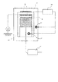
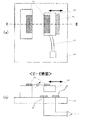
図1は、本発明の第1の実施例の電位測定装置に係るセンサヘッドを示す構成図である。図1(a)は上面図、図1(b)は図1(a)のA-A線における断面図である。図1において、101は、被検知物(図示せず)の電位に応じた電荷量の増減を生じる検知電極、102は一対のコンデンサ電極、103は可動部材、104は、可動部材103を揺動可能に支持する支持部材である。可動部材103は、後述する駆動力発生部(駆動手段)により駆動される。コンデンサ電極102は、可動部材103と支持部材104夫々に略対向して形成され、可動部材103の駆動状態に応じた駆動由来信号を発生する。この駆動由来信号の情報に基づいて、可動部材103の駆動状態が検知され、その検知結果を用いて駆動力発生部が可動部材103の駆動状態を制御する。
(First embodiment)
FIG. 1 is a configuration diagram showing a sensor head according to the potential measuring apparatus of the first embodiment of the present invention. FIG. 1 (a) is a top view, and FIG. 1 (b) is a cross-sectional view taken along line AA in FIG. 1 (a). In FIG. 1, 101 is a detection electrode that increases or decreases the amount of charge according to the potential of an object to be detected (not shown), 102 is a pair of capacitor electrodes, 103 is a movable member, and 104 is swinging the
検知電極101及び一対のコンデンサ電極102は、導電体よりなる電極である。これらの電極は金属板などを貼り付けて形成することが可能である。半導体プロセスで用いられる様な成膜方法により、成膜、パターニングして形成することも容易に可能である。
The
可動部材103と支持部材104は共通の材料で作製することが可能であるが、別々の材料で作製することも可能である。半導体プロセスで用いられる様なシリコンあるいはガラスなどの材料を用いることも可能である。これらの場合、材料としては、導電性、絶縁性何れの材質のものを用いても構わない。導電性の材料を用いる場合、検知電極101及びコンデンサ電極102と、可動部材103及び支持部材104との絶縁を夫々とるために、絶縁層を間に介して作製する。
The
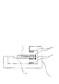
図2は、図1に示す構成に信号処理部などを加えた構成を示す上面図である。検知電極101は、センサ出力信号処理部201と繋がっており、そこで、検知電極101からの増減する電荷量信号が処理される。そして、例えば、センサ出力信号処理部201の後段に控える処理回路でさらに信号処理される。例えば、電位測定装置の被検知物からの測定距離依存性をキャンセルするために用いられるフィードバック処理回路部でセンサ出力信号が処理される。
FIG. 2 is a top view showing a configuration obtained by adding a signal processing unit and the like to the configuration shown in FIG. The
検知電極101に誘起される電荷の量を変化させ、該電荷量の変化から被検知物の電位を測定する一般的な原理は次の通りである。
The general principle of changing the amount of charge induced in the
何らかの手段で被検知物から検知電極に達する電気力線の量が変化すると(以下の説明では、被検知物から見える検知電極の面積(s)が変化するとして説明する)、被検知物と検知電極間に誘起される静電(結合)容量(C)は変化する。
静電容量(C)は一般に式(1)で表すことができる。
C=(ε・s)/g (1)
ここで、εは被検知物と検知電極間の誘電率、gは被検知物と検知電極間の距離、sは被検知物から見える検知電極の面積である。
When the amount of electric field lines reaching the detection electrode from the detected object changes by some means (in the following description, it is assumed that the area (s) of the detection electrode visible from the detected object changes), the detected object and the detection The electrostatic (coupling) capacitance (C) induced between the electrodes varies.
The capacitance (C) can be generally expressed by the formula (1).
C = (ε · s) / g (1)
Here, ε is a dielectric constant between the detection object and the detection electrode, g is a distance between the detection object and the detection electrode, and s is an area of the detection electrode visible from the detection object.
また、静電容量(C)は式(2)でも表すことができる。
Q=C×Vd (2)
ここで、Qは電荷の量、Vdは被検知物の電位である。
式(1)を式(2)に代入すると、式(3)となる。
Q=(ε・s)/g×Vd (3)
The capacitance (C) can also be expressed by equation (2).
Q = C × Vd (2)
Here, Q is the amount of charge, and Vd is the potential of the object to be detected.
Substituting equation (1) into equation (2) yields equation (3).
Q = (ε · s) / g × Vd (3)
ここで、被検知物から見える検知電極の面積が時間(t)に伴って変化する場合、式(3)は式(4)で表すことができる。この変化は、例えば、被検知物と検知電極との間に導電性材料などで形成された遮断板を挿入、引出しすること(後述の第5の実施例などの場合)や両者間の距離の変化(本実施例などの場合)で達成される。
Q(t)=(ε・s(t))/g×Vd (4)
Here, when the area of the detection electrode seen from the object to be detected changes with time (t), the expression (3) can be expressed by the expression (4). This change can be caused, for example, by inserting and pulling out a shielding plate made of a conductive material between the object to be detected and the detection electrode (in the case of the fifth embodiment described later) or the distance between the two. This is achieved by a change (in the case of this example).
Q (t) = (ε · s (t)) / g × Vd (4)
式(4)を時間(t)で微分すると式(5)となる。ここで、時間あたりの面積変化ds(t)/dtは分かっている値である。
dQ(t)/dt=I(t)=(ε/g・ds(t)/dt)×Vd (5)
こうして、式(5)より検知電極からの電流信号I(t)が得られ、この値からVdを求めることができる。また、信号処理精度の向上等を目的として必要に応じてI(t)を電流−電圧変換すれば、電圧出力信号V(t)を得ることができ、出力信号V(t)から被検知物の電位Vdが分かる。また、上記フィードバック処理回路部を用いる方法は、適当な部材(例えば、センサプローブの筐体等)に電圧を印加して、この電圧出力信号V(t)がゼロとなるように調整する。そして、その時の当該印加電圧を被検知物の電位Vdとするものである。
Differentiating equation (4) with respect to time (t) yields equation (5). Here, the area change ds (t) / dt per time is a known value.
dQ (t) / dt = I (t) = (ε / g · ds (t) / dt) × Vd (5)
Thus, the current signal I (t) from the detection electrode is obtained from the equation (5), and Vd can be obtained from this value. Further, if I (t) is subjected to current-voltage conversion for the purpose of improving the signal processing accuracy, etc., the voltage output signal V (t) can be obtained, and the detected object can be obtained from the output signal V (t). Can be obtained. Further, in the method using the feedback processing circuit unit, a voltage is applied to an appropriate member (for example, a housing of the sensor probe) and the voltage output signal V (t) is adjusted to be zero. Then, the applied voltage at that time is set to the potential Vd of the object to be detected.
ここで、コンデンサ電極102について説明する。コンデンサ電極102はその電極間に電位差を生じさせる。図2では可動部材103側のコンデンサ電極102に一定の電位を与えているが、固定部(本実施例では支持部材104)側のコンデンサ電極102に一定の電位を与えても構わない。この場合、センサヘッド駆動時に、検知電極101との位置関係の変わらない方のコンデンサ電極102に一定の電位を与えることで、検知電極101には、オフセット電位が発生することがある。また、固定部側のコンデンサ電極102に一定の電位を与える場合、検知電極101との間に可変なコンデンサを形成し、ノイズ信号としてのってくることがある。何れの場合も、このノイズ信号は特定できるので、トリマーなどで信号を調整することで、除去することは可能である。或いは、後に述べる差動増幅処理でノイズ成分を除去することも可能である。
Here, the
一定の電位を与えない方のコンデンサ電極102はセンサ駆動信号処理部202と繋がっており、そこでコンデンサ電極102からの駆動由来信号が信号処理され、可動部材103の駆動状態(駆動周波数、振幅ないし駆動量)の情報を得る。それら情報より、最適な駆動周波数、駆動用の電力などの駆動信号を発生し、駆動力発生部203に投入する。可動部材103を共振駆動する場合では、最適な駆動信号は、設定された振幅と共振周波数を持つ信号である。共振駆動特性では、周波数が共振周波数から僅かにずれても駆動振幅ないし駆動量は大きく変化する。したがって、駆動周波数と駆動量、または駆動周波数をモニターしていて駆動状態の情報を得て、これらを制御してもよいが、駆動量のみをモニターしていて駆動状態の情報を得て、これに基づいて駆動手段を制御してもよい。この様に、コンデンサ電極102からの駆動由来信号の周期、信号レベルから選択される少なくとも1つに基づいて、必要に応じて可動部材103の駆動状態を検知し、この検知結果を駆動手段にフィードバックすることで、可動部材103の駆動の周期または駆動量またはそれら両方を制御できる。
The
駆動力発生部203により可動部材103を駆動するには、可動部材103に物理的、或いは電気的な力を加える。力としては、例えば、静電引力、電磁力、圧電体素子の歪力、形状記憶合金の形状変化、振動など様々な力を利用することが可能である。駆動力発生部203としては、例えば、可動部材103側に磁石を設置し、支持部材104側にコイルを設置する。コイルに電流を流すと、それに応じた磁場が発生し、その磁場によって磁石に引力、斥力が発生し、可動部材103を駆動させる。この場合、磁石とコイルとの設置関係は逆でも構わないし、両方をコイルとしても構わない。
In order to drive the
静電引力を用いる場合は、可動部材103と支持部材104に電極を対向する様に夫々形成し、そこに電位差を生じさせ、そのときに発生する静電引力により可動部材103を駆動させる。圧電体素子を用いて駆動させる場合は、可動部材103と支持部材104の何れか一方、若しくは両方に圧電体素子を貼付ける。
When electrostatic attraction is used, electrodes are formed on the
図1の構成のセンサヘッドでは、図1(b)の矢印で示す様に、可動部材103が支持部材104で支持される部分をほぼ軸にして片持ち梁式に上下に揺動する。このとき、コンデンサ電極102では、振動に伴う電荷の増減が起こり、駆動由来信号を得ることができる。この信号は上記の如く処理される。
In the sensor head configured as shown in FIG. 1, as indicated by the arrow in FIG. 1B, the
本実施例では、センサ出力信号は、可動部材103の1回の上記上下揺動で1周期の信号が発生する。このとき駆動由来信号については、コンデンサ電極102が電極間距離が最小となる状態と最大となる状態、若しくは、最大面積で対向する状態と最小面積で対向する状態の間を2回経るので、2周期の信号が発生する。こうして、センサ出力信号の周波数と駆動由来信号の周波数との関係は1:2の関係になる。従って、夫々の信号の周期が異なるので、センサ出力信号と駆動由来信号が夫々にとってノイズ成分として影響してくる場合、以下のように対応することができる。例えば、センサ出力信号にバンドパスフィルタをかけることで、S/N比の高いセンサ出力信号を得ることが可能となる。これは、駆動由来信号に対しても同様である。
In the present embodiment, the sensor output signal is generated in one cycle when the
コンデンサ電極102の形状、配置箇所について、本実施例では図1(b)に示す様に平板状のコンデンサ電極102が端面を対向させて可動部材103と支持部材104の端部の上面に夫々形成されている。この構成は、コンデンサ電極102と検知電極101が同一平面上にあるので、MEMSなどの技術を用いて容易に一体的に作製できる利点がある。しかし、例えば、符号102’で示す様に、平板状の電極が平面を対向させて可動部材103と支持部材104の端部の側面に夫々形成される様にしてもよい。この構成によれば、コンデンサ電極102’の対向面積が増えるので、駆動由来信号を増大できる。
With respect to the shape and location of the
図3は、コンデンサ電極301の構成の変形例を示す。図3の様に、コンデンサ形成部を櫛歯形状にすることで、コンデンサ電極301が形成される領域が増えて対向面積が増大する。これによって、駆動由来信号を増大できる。したがって、可動部材103の駆動の制御をより高精度にできる。また、駆動由来信号を増幅するためのオペアンプの選択を安価なものにできる。こうした櫛歯形状の形態は以下の実施例でも適用できるものである。
FIG. 3 shows a modification of the configuration of the
以上に説明した様に、本実施例では、駆動検出手段にコンデンサを用いる。コンデンサは、可動部材と支持部材(固定部)に電極を設けることで、作製することができる。よって、ピエゾ抵抗素子を作製するために、部材の材質を制限されることがなくなる。また、パターニング工程及び拡散工程などの工程が不要になる。また、圧電体素子を貼り付ける工程も不要である。さらには、検知電極を形成する工程で、同時に駆動検出手段となるコンデンサ電極を形成できるので、電位測定装置の製造コストを下げることができる。 As described above, in this embodiment, a capacitor is used as the drive detection means. The capacitor can be manufactured by providing electrodes on the movable member and the support member (fixed portion). Therefore, the material of the member is not limited in order to manufacture the piezoresistive element. In addition, processes such as a patterning process and a diffusion process are not necessary. Further, the step of attaching the piezoelectric element is not necessary. Furthermore, since the capacitor electrode which becomes the drive detection means can be formed at the same time in the step of forming the detection electrode, the manufacturing cost of the potential measuring device can be reduced.
(第2の実施例)
図4は、本発明の第2の実施例の電位測定装置に係るセンサヘッドを示す断面図である。本実施例では、可動部材404と支持部材405の間で、2組のコンデンサ電極が形成されている。2組のコンデンサ電極402、403は、一方の組の電極間が近づくと、他方の組みが離れる構成となっている。これにより、駆動由来信号の位相が略180度ずれたものを得ることができる。これら信号を差動増幅すると、S/N比の高い信号を得ることが可能となる。第2の実施例では、検知電極401からのセンサ出力信号の周波数と各組のコンデンサ電極402、403からの駆動由来信号の周波数との関係は、1:1の関係になる。
(Second embodiment)
FIG. 4 is a cross-sectional view showing a sensor head according to the potential measuring apparatus of the second embodiment of the present invention. In this embodiment, two sets of capacitor electrodes are formed between the
第2の実施例が第1の実施例と異なる点は、コンデンサ電極402、403とこれらを設けた支持部材405の部分とセンサ出力信号の周波数と駆動由来信号の周波数の関係のみで、その他の構成や動作は第1の実施例と同様である。
The second embodiment is different from the first embodiment only in the relationship between the
(第3の実施例)
図5は、本発明の第3の実施例の電位測定装置に係るセンサヘッドを示す構成図である。図5(a)は上面図、図5(b)は図5(a)のB-B線における断面図である。図5において、可動部材504は図5(b)に示す様に、支持部材505に一端を支持されたねじれ軸(トーションバー)504aの回りにねじれ駆動される。そして、検知電極501、502は、ねじれ軸504aに対してほぼ対称的に可動部材504上に設けられている。したがって、一方の検知電極が被検知物に近づくときに他方の検知電極が被検知物から遠ざかる様になる。こうしたねじれ駆動をすることで、検知電極501、502夫々から得られるセンサ出力信号の位相が略180度ずれた関係となり、これら信号を差動増幅することが可能となって、S/N比の高いセンサ出力信号を得ることができる。
(Third embodiment)
FIG. 5 is a configuration diagram showing a sensor head according to the potential measuring apparatus of the third embodiment of the present invention. FIG. 5 (a) is a top view, and FIG. 5 (b) is a cross-sectional view taken along line BB in FIG. 5 (a). In FIG. 5, the
コンデンサ電極503の形状、配置箇所について、本実施例では図5(a)に示す様に平板状の電極が、端面を対向させて可動部材504と支持部材505の端部の上面に夫々形成されている。したがって、本実施例では、センサ出力信号は、可動部材504の1回のねじれ揺動で1周期の信号が発生するが、この間に駆動由来信号は、コンデンサ電極503が最大面積で対向する状態と最小面積で対向する状態の間を2回経るので2周期の信号が発生する。こうして、センサ出力信号の周波数と駆動由来信号の周波数との関係は1:2の関係になる。したがって、本実施例でも、夫々の信号の周期が異なるので、例えば、センサ出力信号にバンドパスフィルタをかけることで、S/N比の高いセンサ出力信号を得ることが可能となる。
With respect to the shape and location of the
第3の実施例が第1の実施例と異なる点は、可動部材504の揺動態様、検知電極501、502の設置態様、センサ出力信号の処理方法のみで、その他の構成や動作は第1の実施例と同様である。
The third embodiment is different from the first embodiment only in the swing mode of the
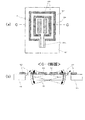
(第4の実施例)
図6は、本発明の第4の実施例の電位測定装置に係るセンサヘッドを示す構成図である。図6(a)は上面図、図6(b)は図6(a)のC-C線における断面図である。本実施例では、図6に示す様に、コンデンサ電極603は可動部材504を囲む様に形成されている。コンデンサ電極603の形成される領域が増えることで、駆動由来信号を増大できる。その他の点は第3の実施例と同じである。
(Fourth embodiment)
FIG. 6 is a configuration diagram showing a sensor head according to the potential measuring apparatus of the fourth embodiment of the present invention. 6 (a) is a top view, and FIG. 6 (b) is a cross-sectional view taken along line CC of FIG. 6 (a). In this embodiment, as shown in FIG. 6, the
尚、図6の構成において、コンデンサ電極をねじれ軸(トーションバー)504aと平行に伸びる部分のみとして、コンデンサ電極をねじれ軸504aを挟んで左右の両側に2組設ける様な変更が可能である。この場合、センサ出力信号の周波数の略2倍の周波数の2つの駆動由来信号が同相で出力されるので、これらを加算して可動部材504の駆動状態を検知することができる。
In the configuration of FIG. 6, it is possible to change the capacitor electrodes so that only two portions extending parallel to the torsion shaft (torsion bar) 504a are provided on the left and right sides of the
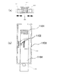
(第5の実施例)
図7は、本発明の第5の実施例の電位測定装置に係るセンサヘッドを示す構成図である。図7(a)は上面図、図7(b)は図7(a)のD-D線における断面図である。本実施例では、図7に示す様に、検知電極702は、固定部である支持部材704側に形成されている。そして、可動部材703は、被検知物(図示せず)と検知電極702との間で形成される電場を変化させる。ここでは、可動部材703は、支持部材704上に一端が固定された可撓性の支持梁705で支持される。上記電場の変化により、被検知物の電位に応じて、検知電極702に生じる電荷の量が変化し、被検知物の電位を検知することが可能となる。
(Fifth embodiment)
FIG. 7 is a configuration diagram showing a sensor head according to the potential measuring apparatus of the fifth embodiment of the present invention. FIG. 7 (a) is a top view, and FIG. 7 (b) is a cross-sectional view taken along the line DD in FIG. 7 (a). In this embodiment, as shown in FIG. 7, the
他方、可動部材703と支持部材704上の固定部に夫々設けられたコンデンサ電極701間に形成されるコンデンサの容量は、可動部材703の動き(図7(b)の矢印参照)に応じて変化する。これにより、可動部材703の動き(駆動状態)に関する情報(変位量、駆動の周期など)を得ることが可能となる。本実施例では、センサ出力信号の周波数と駆動由来信号の周波数との関係は1:1の関係になる。
On the other hand, the capacitance of the capacitor formed between the
可動部材703の駆動するための駆動手段としては、例えば、可動部材703の延長部に電極を設け、この電極と対向して電極を固定側に設けて、これら電極間にアクティブに変調電圧を印加して静電引力で駆動する方法などがある。この場合、図3の櫛歯形状の電極などを好適に用いることができる。電位測定の原理、可動部材703のフィードバック駆動制御などについては、第1の実施例と同様である。
As a driving means for driving the
(第6の実施例)
図8は、本発明の第6の実施例の電位測定装置に係るセンサヘッドを示す構成図である。図8(a)は上面図、図8(b)は図8(a)のE-E線における断面図である。本実施例では、図8に示す様に、検知電極が2つ形成されている。図8において、検知電極801と検知電極802とは、可動部材703の平行移動的な動きによって、被検知物と一方の検知電極の間が遮られるとき、他方の検知電極が遮られない関係となる。これにより、夫々の検知電極801、802から発生する信号の位相は略180度ずれた関係となる。したがって、センサ出力信号を差動増幅することが可能となり、S/N比の高い信号を得ることが可能となる。その他の点は、第5の実施例と同様である。
(Sixth embodiment)
FIG. 8 is a configuration diagram showing a sensor head according to the potential measuring apparatus of the sixth embodiment of the present invention. 8A is a top view, and FIG. 8B is a cross-sectional view taken along the line EE in FIG. 8A. In the present embodiment, as shown in FIG. 8, two detection electrodes are formed. In FIG. 8, the
(第7の実施例)
図9は、本発明の第7の実施例の電位測定装置に係るセンサヘッドを示す構成図である。図9(a)は上面図、図9(b)は図9(a)のF-F線における断面図である。本実施例では、図9に示す様に、コンデンサ電極901、902が可動部材703の移動方向の両側に形成されている。図9において、一方の組のコンデンサ電極間の距離が近づくとき、もう一方の組のコンデンサ電極間の距離が離れる。したがって、各々の組のコンデンサ電極901、902から発生する駆動由来信号の位相は略180度ずれた関係となる。これにより、信号を差動増幅することが可能となり。S/N比の高い駆動由来信号を得ることが可能となる。その他の点は、第5の実施例と同様である。
(Seventh embodiment)
FIG. 9 is a configuration diagram showing a sensor head according to the potential measuring apparatus of the seventh embodiment of the present invention. FIG. 9 (a) is a top view, and FIG. 9 (b) is a cross-sectional view taken along the line FF in FIG. 9 (a). In this embodiment, as shown in FIG. 9,
(第8の実施例)
図10は、図7における可動部材703、検知電極702が複数組並んで配置される構成の第8の実施例を示す上面図である。図10において、並べる組数に比例して、大きなセンサ出力信号を得ることが可能となる。この場合、図7における可動部材703を繋げて1つの可動部材1003とすることにより、夫々の検知電極702に対する可動部材を一度に動かすことができる。これにより、夫々の検知電極702から得られるセンサ出力信号の位相を同じにでき、これらを加算することで大きなセンサ出力信号を得られる。また、可動部材を繋げることにより、一つの可動部材1003を動かせば、それに連れて、繋がった全ての可動部材を一度に動かすことが可能であるので、可動部材用の駆動手段の構成が簡単になる。その他の点は、第5の実施例と同様である。
(Eighth embodiment)
FIG. 10 is a top view showing an eighth embodiment having a configuration in which a plurality of sets of
(第9の実施例)
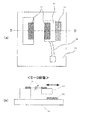
図11は、可動部材1103が、図11(a)の矢印の如く振動するいわゆる音叉型である第9の実施例を示す構成図である。図11(a)は上面図、図11(b)は正面図である。図11において、1101は、被検知物(図示せず)に対向する検知電極、1102はコンデンサ電極、1104はプリント基板(PCB)などの支持部材である。コンデンサ電極1102は、一方の電極が音叉型可動部材1103の一方の腕の内面に設けられ、他方の電極が支持部材1104上の固定部1108に設けられて、可動部材1103の振動に応じの間隔が変化する。音叉型可動部材1103は、その根元部が取付け部1103aを介して支持部材1104に固定されることで、音叉型振動可能に支持部材1104に支持されている。
(Ninth embodiment)
FIG. 11 is a block diagram showing a ninth embodiment in which the
本実施例では、例えば、音叉型可動部材1103に取り付けられた圧電体素子により可動部材1103が駆動されることにより、検知電極1101の被検知物に対して露出する面積が変化してセンサ出力信号が生成される。このとき、コンデンサ電極1102の間隔が変化して駆動由来信号が取り出され、音叉型可動部材1103の駆動状態に関する情報を得ることが可能となる。本実施例では、センサ出力信号の周波数と駆動由来信号の周波数との関係は1:1の関係になる。電位測定の原理、可動部材1003のフィードバック駆動制御などについては、第1の実施例と同様である。
In the present embodiment, for example, when the
上述してきた各実施例は、構成によって、それ単独で利用することも可能であるし、複数の実施例を組み合わせて用いること(例えば、図6のコンデンサ電極の形態を図1の構成に用いること)も可能である。また、上記実施例は電位測定装置として説明したが、図1の構成や図5の構成などは、検知電極に代えて反射ミラーなどの光偏向素子を設けることで、光偏向装置として構成することもできる。こうした光偏向装置では、可動部材の揺動の振幅と周期が高い精度で一定とできるので、光走査幅と走査周期が安定した精度の高い光走査を実現できて、良好な画像形成を達成できる。 Each of the embodiments described above can be used independently depending on the configuration, or a plurality of embodiments can be used in combination (for example, the form of the capacitor electrode in FIG. 6 is used in the configuration in FIG. ) Is also possible. Further, although the above embodiment has been described as a potential measuring device, the configuration of FIG. 1 and the configuration of FIG. 5 can be configured as an optical deflecting device by providing an optical deflecting element such as a reflecting mirror instead of the detection electrode. You can also. In such an optical deflecting device, the amplitude and period of the swing of the movable member can be made constant with high accuracy, so that it is possible to realize high-precision optical scanning with a stable optical scanning width and scanning period, and to achieve good image formation. .
(第10の実施例)
図12は、本発明の電位測定装置が組み込まれた画像形成装置の模式的な構成の一例を示す図である。この画像形成装置は、本発明の電位測定装置1201、帯電器1204、信号処理装置1202、高電圧発生器1203、露光装置1206、トナー供給系1207、被転写物送りローラー1208、感光性ドラム(本発明の電位測定装置で、被検知物と記載するものの一例)1205、被転写物1209の構成よりなる。ここにおいて、画像情報に従って変調される光ビームを走査して感光性ドラム1205に照射するための露光装置1206中に、光走査幅と走査周期が安定した精度の高い光走査を実現できる本発明の光偏向装置を用いることもできる。
(Tenth embodiment)
FIG. 12 is a diagram showing an example of a schematic configuration of an image forming apparatus in which the potential measuring device of the present invention is incorporated. The image forming apparatus includes an electric potential measuring device 1201, a
動作は次の様に行われる。(1)帯電器1204で、ドラム1205を帯電する。(2)露光装置1206で帯電部を露光し、潜像を得る。(3)トナー供給系1207で潜像にトナーを付着させ、トナー像を得る。(4)トナー像を被転写物1209に転写する。(5)被転写物1209上のトナーを溶融して、固着させる。これらの工程を経て画像形成が達成される。この際、ドラム1205の帯電状態を電位測定装置1201で測定し、その結果を信号処理装置1202で処理して、必要に応じて高電圧発生器1203にフィードバックをかける。このことにより、安定したドラム帯電を実現し、安定した良好な画像形成を実現できる。
The operation is performed as follows. (1) The
これら一連の作業を行っていく中で、電位測定装置1201の可動部材の駆動の周期がずれたり変位量(駆動量)が変わったりすると、正確にドラム1205の帯電状態を検知できない。本実施例では、上記コンデンサ電極より、可動部材の駆動状態に関する情報を取得できるため、可動部材の駆動の周期がずれたり変位量が変わったりするのを防止でき、正確にドラム1205の帯電状態を検知できる。こうして、画像形成装置に本発明の電位測定装置を搭載することで、被検知物(ドラム1205)の正確な電位を把握でき、被検知物への帯電処理、現像処理等を高精度にでき、より高品位な画像形成が可能となる。
In the course of these series of operations, if the driving cycle of the movable member of the potential measuring device 1201 shifts or the displacement amount (drive amount) changes, the charged state of the
101、401、501、502、702、801、802、1101・・・検知電極
102、301、402、403、503、603、701、901、902、1102・・・電極(コンデンサ電極、櫛歯形状電極)
103、504、703、1003、1103・・・可動部材
104、405、505、704、1104・・・固定部(支持部材)
201・・・センサ出力信号処理部
202・・・センサ駆動信号処理部
203・・・駆動手段(駆動力発生部)
1205・・・被検知物(ドラム)
101, 401, 501, 502, 702, 801, 802, 1101 ... Detection electrodes
102, 301, 402, 403, 503, 603, 701, 901, 902, 1102 ... Electrode (capacitor electrode, comb-shaped electrode)
103, 504, 703, 1003, 1103 ... movable member
104, 405, 505, 704, 1104 ... fixed part (supporting member)
201 ... Sensor output signal processor
202 ... Sensor drive signal processor
203 ... Drive means (drive force generator)
1205 ... Object to be detected (drum)
Claims (10)
前記可動部材に対して設けられた固定部と、
前記可動部材を駆動するための駆動手段と、
前記可動部材、固定部夫々に形成されてなる、前記駆動手段による前記可動部材の駆動状態に由来する駆動由来信号を発生するための電極と、
を備え、
前記駆動手段が、前記駆動由来信号に基づいて、前記可動部材を共振駆動するように制御することを特徴とする揺動体装置。 A movable member provided to be swingable;
A fixed portion provided for the movable member;
Driving means for driving the movable member;
An electrode for generating a drive-derived signal derived from the drive state of the movable member by the drive means , formed on each of the movable member and the fixed portion;
With
An oscillating body device characterized in that the driving means controls the movable member to resonately drive based on the drive-derived signal.
前記可動部材若しくは固定部に検知電極が形成され、
前記可動部材を共振駆動して被検知物と前記検知電極との間の静電容量を変化させることで、被検知物の電位に応じた電荷量の増減を前記検知電極で生じさせ、
電荷量の増減からセンサ出力信号を得て、被検知物の電位を測定することを特徴とする電位測定装置。 Including the oscillator device according to any one of claims 1 to 6,
A detection electrode is formed on the movable member or the fixed part,
Wherein the movable member resonant drive to by changing the capacitance between the sensing electrode and the detection object, caused by the sensing electrode to increase or decrease the amount of charge corresponding to the potential of the detection object,
A potential measuring device that obtains a sensor output signal from an increase or decrease in the amount of charge and measures the potential of an object to be detected.
前記可動部材に光偏向素子が設けられたことを特徴とする光偏向装置。 Including the oscillator device according to any one of claims 1 to 6,
An optical deflection apparatus, wherein an optical deflection element is provided on the movable member.
Priority Applications (2)
| Application Number | Priority Date | Filing Date | Title |
|---|---|---|---|
| JP2006031806A JP5188024B2 (en) | 2006-02-09 | 2006-02-09 | Oscillator device, potential measuring device, and optical deflection device |
| US11/670,277 US7612569B2 (en) | 2006-02-09 | 2007-02-01 | Oscillating device, electric potential measuring device, light deflecting device, and image forming apparatus |
Applications Claiming Priority (1)
| Application Number | Priority Date | Filing Date | Title |
|---|---|---|---|
| JP2006031806A JP5188024B2 (en) | 2006-02-09 | 2006-02-09 | Oscillator device, potential measuring device, and optical deflection device |
Publications (3)
| Publication Number | Publication Date |
|---|---|
| JP2007212262A JP2007212262A (en) | 2007-08-23 |
| JP2007212262A5 JP2007212262A5 (en) | 2009-03-26 |
| JP5188024B2 true JP5188024B2 (en) | 2013-04-24 |
Family
ID=38333407
Family Applications (1)
| Application Number | Title | Priority Date | Filing Date |
|---|---|---|---|
| JP2006031806A Expired - Fee Related JP5188024B2 (en) | 2006-02-09 | 2006-02-09 | Oscillator device, potential measuring device, and optical deflection device |
Country Status (2)
| Country | Link |
|---|---|
| US (1) | US7612569B2 (en) |
| JP (1) | JP5188024B2 (en) |
Families Citing this family (8)
| Publication number | Priority date | Publication date | Assignee | Title |
|---|---|---|---|---|
| JP2008191537A (en) * | 2007-02-07 | 2008-08-21 | Canon Inc | Vibrating element and light deflector equipped with the same |
| US8345339B2 (en) * | 2007-06-21 | 2013-01-01 | Canon Kabushiki Kaisha | Optical deflector |
| US8054143B2 (en) | 2007-08-16 | 2011-11-08 | Nec Corporation | Switch circuit and semiconductor device |
| CN101514990B (en) * | 2008-02-21 | 2014-01-29 | 天津先阳科技发展有限公司 | Sensor for sensing contents of components to be measured in human tissue fluid, fluid channel unit and method for measuring contents of components to be measured in human tissue fluid |
| US7940040B2 (en) * | 2008-12-19 | 2011-05-10 | Illinois Tool Works Inc. | Foil-leaf electrometer for static field detection with triggered indicator |
| US7915897B2 (en) * | 2008-12-19 | 2011-03-29 | Illinois Tool Works Inc. | Foil-leaf electrometer for static field detection with permanently separating leaves |
| US7924018B2 (en) * | 2008-12-19 | 2011-04-12 | Illinois Tool Works Inc. | MEMS electrometer that measures amount of repulsion of adjacent beams from each other for static field detection |
| US8432049B2 (en) * | 2010-07-15 | 2013-04-30 | Sukho JUNG | Electrical generator |
Family Cites Families (46)
| Publication number | Priority date | Publication date | Assignee | Title |
|---|---|---|---|---|
| US3852667A (en) * | 1973-05-10 | 1974-12-03 | Trek Inc | Probe for electrostatic voltmeter |
| US4205267A (en) * | 1977-11-03 | 1980-05-27 | Williams Bruce T | High speed electrostatic voltmeter |
| US4835461A (en) * | 1984-04-13 | 1989-05-30 | Xerox Corporation | Microdeflector probe for electrostatic voltmeter |
| US4720682A (en) * | 1984-11-29 | 1988-01-19 | Matsushita Electric Industrial Co., Ltd. | Surface electric potential sensor |
| US4763078A (en) * | 1986-03-27 | 1988-08-09 | Williams Bruce T | Sensor for electrostatic voltmeter |
| JP2884447B2 (en) * | 1991-04-22 | 1999-04-19 | キヤノン株式会社 | Cantilever probe, scanning tunneling microscope and information processing device using the same |
| JP2923813B2 (en) * | 1991-06-11 | 1999-07-26 | キヤノン株式会社 | Cantilever displacement element, scanning tunneling microscope using the same, and information processing apparatus |
| JP3184619B2 (en) * | 1991-09-24 | 2001-07-09 | キヤノン株式会社 | Parallel plane holding mechanism and memory device and STM device using the same |
| US5212451A (en) * | 1992-03-09 | 1993-05-18 | Xerox Corporation | Single balanced beam electrostatic voltmeter modulator |
| JP3114397B2 (en) | 1992-10-12 | 2000-12-04 | オムロン株式会社 | Optical device |
| US5489850A (en) * | 1994-05-09 | 1996-02-06 | Xerox Corporation | Balanced beam electrostatic voltmeter modulator employing a shielded electrode and carbon fiber conductors |
| US5455514A (en) * | 1994-06-20 | 1995-10-03 | Eastman Kodak Company | Apparatus and method for measuring polar charge on a sheet or moving web |
| JP3192887B2 (en) * | 1994-09-21 | 2001-07-30 | キヤノン株式会社 | Probe, scanning probe microscope using the probe, and recording / reproducing apparatus using the probe |
| JP3116772B2 (en) | 1995-05-10 | 2000-12-11 | 横河電機株式会社 | EO probe |
| JP3679519B2 (en) * | 1995-09-14 | 2005-08-03 | キヤノン株式会社 | Manufacturing method of micro tip for detecting tunnel current or micro force or magnetic force, manufacturing method of probe having the micro tip, probe thereof, probe unit having the probe, scanning probe microscope, and information recording / reproducing apparatus |
| JP3102320B2 (en) | 1995-09-29 | 2000-10-23 | オムロン株式会社 | Sensor device |
| JP3518099B2 (en) | 1995-10-06 | 2004-04-12 | 株式会社デンソー | Optical scanner device |
| JP3618896B2 (en) * | 1996-03-29 | 2005-02-09 | キヤノン株式会社 | Manufacturing method of probe having minute aperture, probe thereby, combined apparatus of scanning near-field light microscope and scanning tunneling microscope using the probe, and recording / reproducing apparatus using the probe |
| US6101878A (en) * | 1997-03-24 | 2000-08-15 | Denso Corporation | Angular rate sensor and method of improving output characteristic thereof |
| JP3653933B2 (en) | 1997-06-09 | 2005-06-02 | 株式会社村田製作所 | Surface potential detector |
| US6075639A (en) * | 1997-10-22 | 2000-06-13 | The Board Of Trustees Of The Leland Stanford Junior University | Micromachined scanning torsion mirror and method |
| JP3148729B2 (en) * | 1998-04-13 | 2001-03-26 | セイコーインスツルメンツ株式会社 | Ultrasonic motor and electronic equipment with ultrasonic motor |
| JP2000035396A (en) * | 1998-07-16 | 2000-02-02 | Canon Inc | Probe with minute protrusion and its manufacturing method |
| JP2000055670A (en) | 1998-08-07 | 2000-02-25 | Toyota Central Res & Dev Lab Inc | Oscillating type detector |
| US6177800B1 (en) * | 1998-11-10 | 2001-01-23 | Xerox Corporation | Method and apparatus for using shuttered windows in a micro-electro-mechanical system |
| JP4347992B2 (en) | 2000-04-25 | 2009-10-21 | 日本信号株式会社 | Electromagnetic actuator, electromagnetic actuator drive control apparatus and method, electromagnetic actuator resonance frequency signal generation apparatus and method |
| US6504375B1 (en) * | 2000-11-28 | 2003-01-07 | Xerox Corporation | Electrostatic voltmeter modulators and methods of making same |
| US6452399B1 (en) * | 2001-01-29 | 2002-09-17 | Xerox Corporation | Modulator base for electrostatic voltmeter modulator assembly |
| US6831765B2 (en) * | 2001-02-22 | 2004-12-14 | Canon Kabushiki Kaisha | Tiltable-body apparatus, and method of fabricating the same |
| JP2003005124A (en) * | 2001-06-26 | 2003-01-08 | Canon Inc | Optical deflector equipped with displacement detecting function for movable plate, and optical equipment using optical deflector |
| US6600323B2 (en) * | 2001-08-24 | 2003-07-29 | Trek, Inc. | Sensor for non-contacting electrostatic detector |
| US7002719B2 (en) * | 2003-01-15 | 2006-02-21 | Lucent Technologies Inc. | Mirror for an integrated device |
| JP4174345B2 (en) | 2003-03-03 | 2008-10-29 | キヤノン株式会社 | Optical deflector and optical deflector control method |
| JP2004294350A (en) * | 2003-03-28 | 2004-10-21 | Canon Inc | Electric potential sensor and image forming apparatus |
| JP2004294351A (en) | 2003-03-28 | 2004-10-21 | Canon Inc | Electric potential sensor and image forming apparatus |
| JP5027984B2 (en) * | 2003-03-28 | 2012-09-19 | キヤノン株式会社 | Potential measuring apparatus using oscillator, potential measuring method, and image forming apparatus |
| JP2004301554A (en) | 2003-03-28 | 2004-10-28 | Canon Inc | Electric potential measuring device and image forming device |
| JP2005150329A (en) * | 2003-11-14 | 2005-06-09 | Canon Inc | Wiring structure and its forming method |
| JP2005173411A (en) * | 2003-12-12 | 2005-06-30 | Canon Inc | Light deflector |
| JP4174420B2 (en) | 2003-12-15 | 2008-10-29 | キヤノン株式会社 | Optical deflector |
| JP2005338241A (en) * | 2004-05-25 | 2005-12-08 | Canon Inc | Rocking body, image forming apparatus using the same and method of reducing speckle |
| JP2005352300A (en) * | 2004-06-11 | 2005-12-22 | Nippon Signal Co Ltd:The | Optical scanning element and scan optical device using the same |
| JP2006003130A (en) * | 2004-06-15 | 2006-01-05 | Canon Inc | Electric potential measuring apparatus and image forming apparatus |
| JP2006003131A (en) * | 2004-06-15 | 2006-01-05 | Canon Inc | Potential sensor |
| US7049804B2 (en) * | 2004-07-12 | 2006-05-23 | Canon Kabushiki Kaisha | Electric potential measuring apparatus, and image forming apparatus |
| JP2006162457A (en) * | 2004-12-08 | 2006-06-22 | Canon Inc | Electric potential measuring device and image forming apparatus |
-
2006
- 2006-02-09 JP JP2006031806A patent/JP5188024B2/en not_active Expired - Fee Related
-
2007
- 2007-02-01 US US11/670,277 patent/US7612569B2/en not_active Expired - Fee Related
Also Published As
| Publication number | Publication date |
|---|---|
| US20070182419A1 (en) | 2007-08-09 |
| JP2007212262A (en) | 2007-08-23 |
| US7612569B2 (en) | 2009-11-03 |
Similar Documents
| Publication | Publication Date | Title |
|---|---|---|
| JP5188024B2 (en) | Oscillator device, potential measuring device, and optical deflection device | |
| JP5027984B2 (en) | Potential measuring apparatus using oscillator, potential measuring method, and image forming apparatus | |
| KR100901237B1 (en) | Optical deflector and optical instrument using the same | |
| JP2007199682A (en) | Optical deflector and light beam scanning apparatus | |
| JP3882972B2 (en) | Angular velocity sensor | |
| KR20000029967A (en) | Angular velocity detector | |
| JP2000329681A (en) | Self-exciation and self-detection-type probe and scanning probe device | |
| US7372278B2 (en) | Electric potential measuring apparatus electrostatic capacitance measuring apparatus, electric potential measuring method, electrostatic capacitance measuring method, and image forming apparatus | |
| JP4886495B2 (en) | Potential measuring apparatus and image forming apparatus | |
| JPH10300478A (en) | Angular velocity detecting element and angular velocity measuring device | |
| WO2010041422A1 (en) | Angular velocity sensor element, angular velocity sensor and angular velocity sensor unit both using angular velocity sensor element, and signal detecting method for angular velocity sensor unit | |
| JP3264580B2 (en) | Angular velocity detector | |
| CN112088483A (en) | Electrostatic actuator and physical quantity sensor | |
| JP2006003130A (en) | Electric potential measuring apparatus and image forming apparatus | |
| JP4320934B2 (en) | Semiconductor angular velocity sensor | |
| JP2008225041A (en) | Method of driving and controlling optical scanner, and driving and controlling apparatus | |
| US7690046B2 (en) | Drive stage for scanning probe apparatus, and scanning probe apparatus | |
| JPH08334332A (en) | Vibration gyro | |
| JP4950574B2 (en) | Potential measuring apparatus and potential measuring method | |
| JP2004301575A (en) | Angular velocity sensor | |
| JP2007046981A (en) | Electric potential measuring apparatus and image forming apparatus | |
| JP2007298451A (en) | Potential measuring instrument, and image forming device equipped with potential measuring instrument | |
| JP2009074948A (en) | Oscillating body apparatus, potential measurement apparatus using same and image forming apparatus | |
| JP2005140798A (en) | Angular velocity measuring system | |
| JP2006337161A (en) | Rotation vibration device and potential measuring device |
Legal Events
| Date | Code | Title | Description |
|---|---|---|---|
| A521 | Request for written amendment filed |
Free format text: JAPANESE INTERMEDIATE CODE: A523 Effective date: 20090209 |
|
| A621 | Written request for application examination |
Free format text: JAPANESE INTERMEDIATE CODE: A621 Effective date: 20090209 |
|
| A131 | Notification of reasons for refusal |
Free format text: JAPANESE INTERMEDIATE CODE: A131 Effective date: 20120315 |
|
| A521 | Request for written amendment filed |
Free format text: JAPANESE INTERMEDIATE CODE: A523 Effective date: 20120507 |
|
| TRDD | Decision of grant or rejection written | ||
| A01 | Written decision to grant a patent or to grant a registration (utility model) |
Free format text: JAPANESE INTERMEDIATE CODE: A01 Effective date: 20130108 |
|
| A61 | First payment of annual fees (during grant procedure) |
Free format text: JAPANESE INTERMEDIATE CODE: A61 Effective date: 20130122 |
|
| FPAY | Renewal fee payment (event date is renewal date of database) |
Free format text: PAYMENT UNTIL: 20160201 Year of fee payment: 3 |
|
| FPAY | Renewal fee payment (event date is renewal date of database) |
Free format text: PAYMENT UNTIL: 20160201 Year of fee payment: 3 |
|
| LAPS | Cancellation because of no payment of annual fees |