JP2005173411A - Light deflector - Google Patents
Light deflector Download PDFInfo
- Publication number
- JP2005173411A JP2005173411A JP2003415786A JP2003415786A JP2005173411A JP 2005173411 A JP2005173411 A JP 2005173411A JP 2003415786 A JP2003415786 A JP 2003415786A JP 2003415786 A JP2003415786 A JP 2003415786A JP 2005173411 A JP2005173411 A JP 2005173411A
- Authority
- JP
- Japan
- Prior art keywords
- movable
- gimbal
- fixed
- movable mirror
- electrode
- Prior art date
- Legal status (The legal status is an assumption and is not a legal conclusion. Google has not performed a legal analysis and makes no representation as to the accuracy of the status listed.)
- Pending
Links
Images


Classifications
-
- G—PHYSICS
- G02—OPTICS
- G02B—OPTICAL ELEMENTS, SYSTEMS OR APPARATUS
- G02B26/00—Optical devices or arrangements for the control of light using movable or deformable optical elements
- G02B26/08—Optical devices or arrangements for the control of light using movable or deformable optical elements for controlling the direction of light
- G02B26/0816—Optical devices or arrangements for the control of light using movable or deformable optical elements for controlling the direction of light by means of one or more reflecting elements
- G02B26/0833—Optical devices or arrangements for the control of light using movable or deformable optical elements for controlling the direction of light by means of one or more reflecting elements the reflecting element being a micromechanical device, e.g. a MEMS mirror, DMD
- G02B26/085—Optical devices or arrangements for the control of light using movable or deformable optical elements for controlling the direction of light by means of one or more reflecting elements the reflecting element being a micromechanical device, e.g. a MEMS mirror, DMD the reflecting means being moved or deformed by electromagnetic means
-
- G—PHYSICS
- G02—OPTICS
- G02B—OPTICAL ELEMENTS, SYSTEMS OR APPARATUS
- G02B26/00—Optical devices or arrangements for the control of light using movable or deformable optical elements
- G02B26/08—Optical devices or arrangements for the control of light using movable or deformable optical elements for controlling the direction of light
- G02B26/0816—Optical devices or arrangements for the control of light using movable or deformable optical elements for controlling the direction of light by means of one or more reflecting elements
- G02B26/0833—Optical devices or arrangements for the control of light using movable or deformable optical elements for controlling the direction of light by means of one or more reflecting elements the reflecting element being a micromechanical device, e.g. a MEMS mirror, DMD
- G02B26/0841—Optical devices or arrangements for the control of light using movable or deformable optical elements for controlling the direction of light by means of one or more reflecting elements the reflecting element being a micromechanical device, e.g. a MEMS mirror, DMD the reflecting element being moved or deformed by electrostatic means
Landscapes
- Physics & Mathematics (AREA)
- General Physics & Mathematics (AREA)
- Optics & Photonics (AREA)
- Electromagnetism (AREA)
- Mechanical Optical Scanning Systems (AREA)
- Mechanical Light Control Or Optical Switches (AREA)
- Micromachines (AREA)
- Facsimile Heads (AREA)
- Facsimile Scanning Arrangements (AREA)
- Laser Beam Printer (AREA)
Abstract
Description
本発明は、マイクロメカニクスの手法などにて作製される光偏向器に関するものである。 The present invention relates to an optical deflector manufactured by a micromechanics technique or the like.
近年、マイクロメカニクス技術を用いたマイクロアクチュエータの開発が盛んである。駆動手段は静電駆動・圧電駆動・電磁駆動等がある。こうしたマイクロアクチュエータに対しては、コストダウンやモバイル機器等への需要に伴い、小型化・大出力(小電力で比較的大きな偏向角を得られること)の要請が強くなってきている。特に、2つのトーションバー(ねじり梁)で支持された可動ミラーを偏向させる光偏向器は、簡便な構成で光センサーや画像形成装置を形成することが可能なデバイスとして開発が進んでいる。 In recent years, development of microactuators using micromechanics technology has been active. Driving means include electrostatic driving, piezoelectric driving, electromagnetic driving, and the like. For such microactuators, demands for downsizing and large output (relatively large deflection angle can be obtained with small electric power) are increasing with the demand for cost reduction and mobile devices. In particular, an optical deflector that deflects a movable mirror supported by two torsion bars (twisted beams) has been developed as a device that can form an optical sensor and an image forming apparatus with a simple configuration.
この様な構成の可動ミラーを駆動する方法としては、まず、図6に断面図と平面図で示すように対向電極と可動ミラーとの間に働く静電力により可動ミラーをトーションバーの回転軸の回りで偏向(変位)させる方法がある(特許文献1参照)。また、図7に示すように可動ミラー上に櫛型電極を形成し、これと隙間を隔てて互いに噛み合うように櫛型電極を配置し、2つの櫛型電極の間に働く静電力により可動ミラーをトーションバーの回転軸の回りで偏向させる方法がある(特許文献2参照)。また、図8に示すように可動ミラー上にコイルを配線し、コイルの近傍に永久磁石を配置し、コイルに電流を流すことで発生する磁場が永久磁石と作用することにより可動ミラーをトーションバーの回転軸の回りで偏向させる、ムービングコイルと呼ばれる方法がある(特許文献3参照)。また、図9に示すように可動ミラー上に磁石を配置し、磁石の近傍にコイルを配置し、コイルに電流を流すことで発生する磁場が永久磁石と作用することにより可動ミラーをトーションバーの回転軸の回りで偏向させる、ムービングマグネットと呼ばれる方法がある(特開平6−82711)。 As a method of driving the movable mirror having such a configuration, first, as shown in a cross-sectional view and a plan view in FIG. 6, the movable mirror is moved by the electrostatic force acting between the counter electrode and the movable mirror. There is a method of deflecting (displacement) around (see Patent Document 1). In addition, as shown in FIG. 7, a comb-shaped electrode is formed on the movable mirror, and the comb-shaped electrode is disposed so as to mesh with each other with a gap therebetween, and the movable mirror is driven by an electrostatic force acting between the two comb-shaped electrodes. Is deflected around the rotation axis of the torsion bar (see Patent Document 2). Further, as shown in FIG. 8, a coil is wired on the movable mirror, a permanent magnet is disposed in the vicinity of the coil, and a magnetic field generated by passing an electric current through the coil acts on the permanent magnet so that the movable mirror is moved to the torsion bar. There is a method called a moving coil that deflects around the rotation axis (see Patent Document 3). Further, as shown in FIG. 9, a magnet is arranged on the movable mirror, a coil is arranged in the vicinity of the magnet, and a magnetic field generated by passing an electric current through the coil acts on the permanent magnet so that the movable mirror is placed on the torsion bar. There is a method called a moving magnet that deflects around a rotation axis (Japanese Patent Laid-Open No. 6-82711).
さらに、図10に示すように上記のような偏向器を二軸偏向可能に配置した構造のアクチュエータも開発されている(特許文献5参照)。すなわち、可動ミラーが2つのトーションバーでジンバル(可動な基板ないしフレーム)に支持され、ジンバルが他の2つのトーションバーで基板に支持され、可動ミラーとジンバルとの駆動軸が互いに直交する構造を有しており、可動部と二対の対向電極との間の静電力により可動部を駆動する。ここには、磁気的な手段による可動部の駆動も開示されている。この構成においては、可動ミラーとジンバルとの共振周波数を所望の値にして、ラスタ走査による画像形成が可能な二軸光偏向器を提供することができる。
上記のようなジンバル構造を有するアクチュエータにおいて、二軸の回りの駆動を静電駆動で行う場合、対向電極であるか櫛型電極であるか、また、その他の方法であるかに関わらず、二軸駆動のためにそれぞれの電極を配置する為、互いの作る電場のクロストークが問題となる。同様に、二軸の回りの駆動を電磁駆動で行う場合、ムービングマグネットであるかムービングコイルであるか、また、その他の方法であるかに関わらず、二軸駆動のためにそれぞれの永久磁石や電磁コイルを配置する為、磁石の配置の制限や、互いの作る磁場のクロストークが問題となる。また、一方の駆動が対向電極による静電駆動の場合、対向電極の構造上の欠点として、可動部駆動用発生力と可動部変位量とのどちらかを犠牲にしなければならない。すなわち、変位量が大きく取れるように電極間距離を大きくすると所望の変位角を得る為の駆動電圧が高くなるという問題点がある。 In the actuator having the gimbal structure as described above, when driving around two axes is performed by electrostatic driving, it does not matter whether it is a counter electrode, a comb electrode, or any other method. Since each electrode is arranged for axial driving, crosstalk of electric fields generated by each other becomes a problem. Similarly, when driving around two axes by electromagnetic driving, regardless of whether it is a moving magnet, a moving coil, or other methods, each permanent magnet or Since the electromagnetic coil is arranged, there are problems in limiting the arrangement of the magnets and crosstalk between the magnetic fields generated by each other. In addition, when one drive is electrostatic drive using a counter electrode, as a drawback of the structure of the counter electrode, one of the generated force for driving the movable part and the amount of displacement of the movable part must be sacrificed. That is, there is a problem that the drive voltage for obtaining a desired displacement angle increases when the distance between the electrodes is increased so that the displacement amount can be increased.
上記課題に鑑み、本発明の光偏向器は、可動ミラーと、該可動ミラーを第1の支持部により回転軸の回りで揺動可能に支持するジンバルと、該ジンバルを第2の支持部により該可動ミラーの回転軸と角度をなす回転軸の回りで揺動可能に支持するフレームと、前記ジンバル上の該ジンバルの揺動方向とほぼ平行な面を持つ可動電極と、該可動電極の面と対向し合うように配置された固定電極と、可動電極と固定電極との間に働く静電力により該ジンバルを変位させる静電駆動手段と、電磁力により該可動ミラーを変位させる電磁駆動手段とを有することを特徴とする。 In view of the above problems, an optical deflector of the present invention includes a movable mirror, a gimbal that supports the movable mirror by a first support portion so as to be swingable around a rotation axis, and the gimbal that is supported by a second support portion. A frame that is pivotably supported around a rotation axis that forms an angle with the rotation axis of the movable mirror, a movable electrode having a surface substantially parallel to a swing direction of the gimbal on the gimbal, and a surface of the movable electrode A fixed electrode disposed so as to face each other, electrostatic drive means for displacing the gimbal by electrostatic force acting between the movable electrode and the fixed electrode, and electromagnetic drive means for displacing the movable mirror by electromagnetic force It is characterized by having.
上記基本構成に基づいて、以下の様な態様が可能である。
前記可動電極が可動櫛型電極であり、前記固定電極が、可動櫛型電極と隙間を隔てて互いに噛み合うように配置される固定櫛型電極である様にできる。或いは、ジンバルの両端部(ジンバルの回転軸に直交する方向の両端)に設けた可動電極に、ジンバルの揺動方向とほぼ平行な比較的広い面積の平面を持たせ、これと対向して比較的広い面積の平面を固定電極に持たせる様な態様にすることも可能である。また、第1の支持部が、ジンバルに対して可動ミラーを回転軸の回りでねじり回転可能に支持する2つのトーションバーであり、第2の支持部が、フレームに対してジンバルを、可動ミラーの回転軸と直交する回転軸の回りでねじり回転可能に支持する2つのトーションバーである様にできる。ねじり回転可能なトーションバーを用いる場合、共振駆動を容易に実現できて高速走査が可能となる。勿論、支持部としては、可動ミラーやジンバルを揺動可能に支持するものであればどの様なものでもよく、また、可動ミラーの回転軸とジンバルの回転軸は角度をなしていれば、直角以外の角度で交差する様になっていてもよい。
Based on the above basic configuration, the following modes are possible.
The movable electrode may be a movable comb electrode, and the fixed electrode may be a fixed comb electrode disposed so as to mesh with the movable comb electrode with a gap therebetween. Alternatively, the movable electrodes provided at both ends of the gimbal (both ends in the direction orthogonal to the rotational axis of the gimbal) have a relatively large area plane almost parallel to the swinging direction of the gimbal, and are compared with this. It is also possible to adopt a mode in which the fixed electrode has a plane with a large area. Further, the first support part is two torsion bars that support the movable mirror so that the movable mirror can be torsionally rotated around the rotation axis with respect to the gimbal, and the second support part supports the gimbal with respect to the frame. It is possible to provide two torsion bars that support torsional rotation around a rotation axis orthogonal to the rotation axis. When a torsion bar capable of twisting rotation is used, resonance driving can be easily realized and high-speed scanning is possible. Of course, the support portion may be any member that supports the movable mirror and the gimbal so that the movable mirror and the gimbal can oscillate. You may be allowed to cross at an angle other than.
また、前記電磁駆動手段は、固定コイルと、可動ミラー上に配置される可動磁石とを有し、固定コイルと可動磁石との間に働く電磁力により該可動ミラーを変位させる構成を有したり、少なくとも1つ以上の固定磁石と、可動ミラー上に配置される可動コイルとを有し、固定磁石と可動コイルとの間に働く電磁力により該可動ミラーを変位させる構成を有したりする。この場合、前記固定磁石が複数であり、かつ、ジンバルの回転軸と平行に一列に離散的に配置されている態様にできる。こうした構成により、偏向角を大きく取れる。 In addition, the electromagnetic drive unit includes a fixed coil and a movable magnet disposed on the movable mirror, and has a configuration for displacing the movable mirror by an electromagnetic force acting between the fixed coil and the movable magnet. And having at least one fixed magnet and a movable coil disposed on the movable mirror, and having a configuration in which the movable mirror is displaced by electromagnetic force acting between the fixed magnet and the movable coil. In this case, a plurality of the fixed magnets can be provided and discretely arranged in a line parallel to the rotation axis of the gimbal. With this configuration, a large deflection angle can be obtained.
また、前記フレーム、固定電極、固定コイルが形成されたコイル基板、固定磁石のうちの少なくとも1つが共通基板に支持されている構成にもできる。この場合、前記固定電極、コイル基板、固定磁石のうちの少なくとも1つが共通基板に形成された凹部に設置されている様にできる。この構成において、固定電極が共通基板上に形成された取り出し電極上に設置されている構成や、フレームがスペーサを介して共通基板に支持されている構成を採り得る。 Further, at least one of the frame, the fixed electrode, the coil substrate on which the fixed coil is formed, and the fixed magnet may be supported by a common substrate. In this case, at least one of the fixed electrode, the coil substrate, and the fixed magnet can be installed in a recess formed in the common substrate. In this configuration, a configuration in which the fixed electrode is installed on the extraction electrode formed on the common substrate, or a configuration in which the frame is supported on the common substrate through the spacer can be adopted.
また、前記電磁駆動手段と静電駆動手段の少なくとも一方が、可動ミラーまたはジンバルを共振駆動させる手段である様にもできる。 Further, at least one of the electromagnetic driving means and the electrostatic driving means may be means for resonantly driving the movable mirror or gimbal.
更に、上記課題に鑑み、本発明の画像形成装置は、光源、該光源からの光を偏向する上記の光偏向器を具備し、該光偏向器からの光で画像を形成することを特徴とする。 Further, in view of the above problems, an image forming apparatus of the present invention includes a light source and the above-described optical deflector that deflects light from the light source, and forms an image with the light from the optical deflector. To do.
本発明により、比較的変位角を大きくでき、比較的低電圧で駆動でき、コンパクトな構成にでき、高速走査が可能で、二軸それぞれの駆動信号間のクロストークを低減できるジンバル構造による二軸駆動光偏向器を実現できる。すなわち、ジンバルの揺動方向とほぼ平行な面同士で対向し合う可動電極と固定電極による静電駆動を用いるので比較的変位角を大きくでき、電磁力により可動ミラーを変位させる電磁駆動を用いるので比較的低電圧で駆動でき、こうした静電駆動手段や電磁駆動手段を用いるのでコンパクトな構成にでき、可動ミラーを変位させるのに電磁駆動を用いることでその慣性モーメントを比較的小さくできて高速走査が可能となり、二軸それぞれの駆動力の性質を異ならせているのでクロストークを低減できる。また、共通基板に凹部を形成する場合、そこに配置する固定電極や固定コイルや固定磁石の位置精度を向上させることができる。また、ジンバルの回転軸と平行な方向に固定磁石を離散的に一列に配置する場合、二軸の偏向角を共に大きくすることができる。更に、本発明により、コンパクトな構成にでき、比較的低電圧で駆動でき、比較的偏向角を大きくでき、高精細な画像が得られる画像形成装置を実現できる。 The present invention enables a relatively large displacement angle, can be driven at a relatively low voltage, can have a compact configuration, can perform high-speed scanning, and can reduce crosstalk between the drive signals of the two axes. A driving light deflector can be realized. That is, since the electrostatic drive by the movable electrode and the fixed electrode facing each other on the plane almost parallel to the swinging direction of the gimbal is used, the displacement angle can be relatively large, and the electromagnetic drive that displaces the movable mirror by the electromagnetic force is used. It can be driven at a relatively low voltage, and since it uses such electrostatic drive means and electromagnetic drive means, it can be made compact, and by using electromagnetic drive to displace the movable mirror, its moment of inertia can be made relatively small and high-speed scanning can be achieved. Crosstalk can be reduced because the driving force characteristics of the two axes are made different. Moreover, when forming a recessed part in a common board | substrate, the positional accuracy of the fixed electrode arrange | positioned there, a fixed coil, or a fixed magnet can be improved. Further, when the fixed magnets are discretely arranged in a line in a direction parallel to the rotational axis of the gimbal, both the biaxial deflection angles can be increased. Furthermore, according to the present invention, it is possible to realize an image forming apparatus that can be made compact, can be driven at a relatively low voltage, can have a relatively large deflection angle, and can obtain a high-definition image.
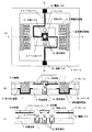
上述した様に、本発明は、ジンバル構造を有する二軸光偏向器において、ジンバル(可動な第1の基板)の揺動方向とほぼ平行な面を持つ電極(櫛型電極など)による静電駆動でジンバルを固定の第2の基板に対して揺動駆動し、かつ、可動ミラーを電磁駆動でジンバルに対して揺動駆動することを特徴とする。こうした特徴を有する本発明による光偏向器の一実施形態について、図1を用いて説明する。図1(a)は、光偏向器の反射面と反対側の面から見た可動部分の構成図、図1(b)はA-A’断面図である。 As described above, in the biaxial optical deflector having a gimbal structure, the present invention is based on an electrostatic force generated by an electrode (such as a comb electrode) having a plane substantially parallel to the swinging direction of the gimbal (movable first substrate). It is characterized in that the gimbal is driven to swing relative to the fixed second substrate by driving, and the movable mirror is driven to swing relative to the gimbal by electromagnetic driving. An embodiment of the optical deflector according to the present invention having such characteristics will be described with reference to FIG. FIG. 1A is a configuration diagram of a movable part viewed from a surface opposite to the reflection surface of the optical deflector, and FIG. 1B is a cross-sectional view taken along line A-A ′.
本実施形態では、反射膜11を備えた可動ミラー1が、2つのトーションバー2により、ジンバル3にねじり回転可能に支持されている。ジンバル3は、他の2つのトーションバー4により、可動ミラー1の回転軸と直交する軸方向にねじり回転可能にフレーム5に支持されている。ジンバル3には2つの可動櫛型電極6が形成され、可動櫛型電極6と適当な隙間を隔てて互いに噛み合うように2つの固定櫛型電極7が配置されている。2つの固定櫛型電極7は取り出し電極8を介して共通基板9上に配置されている。また、フレーム5はスペーサ10を介して共通基板9に接合されている。こうして、ジンバル3は静電力で駆動される。
In this embodiment, the movable mirror 1 including the reflective film 11 is supported by the two
一方、可動ミラー1は電磁力により駆動される。この電磁力は、可動ミラー1上の磁石20と、コイル基板22、取り出し電極23を介して共通基板9上に配置された固定コイル21との間で発生する。この構成では、コイル基板22により固定コイル21は磁石20に接近して配置できて、電磁力は有効に磁石20に作用する。図1においては固定コイル21の作る磁場により可動ミラー1上の磁石20が力を受けて変位するが、可動ミラー上のコイルに流れる電流が固定磁石の作る磁場と作用して変位する方法も、同様に用いることが可能である。
On the other hand, the movable mirror 1 is driven by electromagnetic force. This electromagnetic force is generated between the
本実施形態においては、上記した様にジンバル3を櫛型電極6、7による静電駆動で駆動するが、櫛型電極駆動では、櫛歯のピッチや対向面積の設計により、背景技術ところで説明した対向電極より低電圧にでき、かつ、変位量を大きくできる。特に、ジンバル3は可動ミラー1と比較して端の辺の長さが大きいので、櫛歯の本数を多くできる為、駆動用発生力を大きくすることが可能である。
In the present embodiment, as described above, the gimbal 3 is driven by electrostatic drive using the
他方、ラスタ走査の高速走査に対応する可動ミラー1の揺動は電磁駆動によるので、櫛型電極のジンバル3と比較して可動ミラー1の慣性モーメントを小さくでき、その共振周波数を高くできる。この結果、可動ミラー1は小型でかつ高速走査が可能となる。また、電磁駆動の特徴として比較的低電圧で駆動でき、可動体1が高電圧にならないので、ショートの問題が無いという利点がある。さらに、可動ミラー1を電磁駆動、ジンバル3を櫛型電極による静電駆動とすることで二軸それぞれの駆動信号間のクロストークを低減でき、高性能なデバイスを提供できる。 On the other hand, the swinging of the movable mirror 1 corresponding to the high-speed scanning of the raster scan is based on electromagnetic drive, so that the moment of inertia of the movable mirror 1 can be reduced and its resonance frequency can be increased as compared with the gimbal 3 of the comb electrode. As a result, the movable mirror 1 is small and can be scanned at high speed. Further, as a feature of electromagnetic drive, there is an advantage that there is no short circuit problem because the movable body 1 can be driven at a relatively low voltage and the movable body 1 does not become a high voltage. Furthermore, by making the movable mirror 1 electromagnetically driven and the gimbal 3 electrostatically driven by comb electrodes, crosstalk between the drive signals of the two axes can be reduced, and a high-performance device can be provided.
図2は本実施形態による光偏向器の駆動の様子を示したものである。図2(a)は駆動前の状態(中立の状態)、図2(b)はジンバル3を偏向させた状態、図2(c)はジンバル3と可動ミラー1との両方を偏向させた状態である。すなわち、可動ミラー1およびジンバル3を支持するそれぞれのトーションバー2、4が捻れることにより、可動ミラー1およびジンバル3が偏向する。こうして、可動ミラー1の偏向にはジンバル3の偏向が重畳され、可動ミラー1の二次元的な偏向が可能となる。偏向には後述するDC駆動を用いてもよいが、可動ミラー1およびジンバル3それぞれの共振振動を利用することにより、比較的小さい消費電力で可動ミラー1を駆動できる。
FIG. 2 shows how the optical deflector according to this embodiment is driven. 2A is a state before driving (neutral state), FIG. 2B is a state where the gimbal 3 is deflected, and FIG. 2C is a state where both the gimbal 3 and the movable mirror 1 are deflected. It is. That is, when the
本発明の光偏向器においては、また、固定櫛型電極と共通基板とを別体で形成し、固定櫛型電極を共通基板上に設置した構成をも採り得る(図3等参照)。この構成により、固定櫛型電極と可動櫛型電極との位置関係を任意に設計できる。また、固定櫛型電極やコイル基板や固定磁石を共通基板上の凹部に設置することにより、位置制御を容易にすることが可能となる。 In the optical deflector of the present invention, a configuration in which the fixed comb electrode and the common substrate are formed separately and the fixed comb electrode is installed on the common substrate can also be adopted (see FIG. 3 and the like). With this configuration, the positional relationship between the fixed comb electrode and the movable comb electrode can be arbitrarily designed. Further, the position control can be facilitated by installing the fixed comb electrode, the coil substrate, and the fixed magnet in the concave portion on the common substrate.
本発明の光偏向器においては、また、固定磁石をジンバルの回転軸と平行に一列に配置した構成をも採り得る(図4等参照)。この配置方法により、ジンバルの変位の影響を受けずに可動ミラーを偏向させることができる。 In the optical deflector of the present invention, it is also possible to adopt a configuration in which fixed magnets are arranged in a line parallel to the rotational axis of the gimbal (see FIG. 4 and the like). With this arrangement method, the movable mirror can be deflected without being affected by the displacement of the gimbal.
本発明は、また、本発明の光偏向器を用いた画像形成装置をも対象とする。本発明による低電圧駆動が可能で、高速走査に対応でき、変位角を大きく取れる光偏向器を用いることで、小型かつ低コストで、消費電力が小さく、解像度の高い画像形成装置を実現することが可能となる。 The present invention is also directed to an image forming apparatus using the optical deflector of the present invention. By using an optical deflector that can be driven at a low voltage according to the present invention, can cope with high-speed scanning, and has a large displacement angle, a small, low-cost, low power consumption, high-resolution image forming apparatus can be realized. Is possible.
以下、具体的な実施例を挙げて本発明を詳細に説明する。 Hereinafter, the present invention will be described in detail with specific examples.
(実施例1)
本実施例は本発明による光偏向器の第一態様である。図1にその構成を示す。その概略構成は上記実施形態のところで説明した通りである。本実施例において、可動ミラー1、トーションバー2、ジンバル3、トーションバー4、およびフレーム5は、厚さ150μmのシリコン基板をエッチング加工することにより一体形成される。可動ミラー1上には、反射膜11が形成され、また、可動ミラー1の反射膜11と反対面上には2つの可動磁石20が接合されている。
(Example 1)
This embodiment is a first embodiment of the optical deflector according to the present invention. FIG. 1 shows the configuration. The general configuration is as described in the above embodiment. In this embodiment, the movable mirror 1, the
固定コイル21は、コイル基板22上に形成され、コイル基板22は2つの取り出し電極23を介して共通基板9上に配置されている。2つの取り出し電極23は、それぞれコイル基板22に形成された貫通配線を経由して、固定コイル21の最内周と最外周とに接続される。 The fixed coil 21 is formed on the coil substrate 22, and the coil substrate 22 is disposed on the common substrate 9 via the two extraction electrodes 23. The two extraction electrodes 23 are connected to the innermost periphery and the outermost periphery of the fixed coil 21 through through wirings formed in the coil substrate 22, respectively.
本実施例による光偏向器は、さらに、可動櫛型電極6と固定櫛型電極7との間に電位差を発生させ、可動櫛型電極6と固定櫛型電極7との間に働く静電力によりジンバル3を駆動させる静電駆動手段(不図示)と、固定コイル21に電流を流すことで発生する磁場が可動磁石20に作用することにより可動ミラー1を駆動させる電磁駆動手段(不図示)とを有している。
The optical deflector according to the present embodiment further generates a potential difference between the
本実施例の駆動方法を説明する。本実施例においては、可動ミラー1およびジンバル3を共振駆動により駆動させる。まず、ジンバル3の駆動方法について説明する。駆動電源と制御回路よりなる静電駆動手段により、可動櫛型電極6と固定櫛型電極7との間にジンバル3のねじり振動周波数と同じ周波数の交流電圧を印加して、ジンバル3を振動させる。
A driving method of this embodiment will be described. In this embodiment, the movable mirror 1 and the gimbal 3 are driven by resonance driving. First, a method for driving the gimbal 3 will be described. By applying electrostatic drive means comprising a drive power source and a control circuit, an alternating voltage having the same frequency as the torsional vibration frequency of the gimbal 3 is applied between the
この共振駆動されるジンバル3の外形寸法は4×10mm、厚さは150μmとする。ジンバル3用のトーションバー4の長さは5mm、幅は20μm、厚さは150μmとする。また、ジンバル3は一回往復振動する間にラスタ走査の2フレームを描画する様にする。ここでのフレームレートは60Hzで、従ってジンバル3の共振周波数は30Hzである。偏向角は±10°とする。 The external dimensions of the resonantly driven gimbal 3 are 4 × 10 mm and the thickness is 150 μm. The length of the torsion bar 4 for the gimbal 3 is 5 mm, the width is 20 μm, and the thickness is 150 μm. The gimbal 3 draws two frames of raster scanning while reciprocating once. The frame rate here is 60 Hz, and therefore the resonant frequency of the gimbal 3 is 30 Hz. The deflection angle is ± 10 °.
さらに、ジンバル3の慣性モーメントIは約1×10⁻¹⁰ [kgm2]、トーションバー4のばね定数k は約3.6×10⁻⁶ [Nm] とする。その共振のQ値は約100であり、偏向角±10°の振動に必要なトルクを求めると約5×10⁻⁹
[kgm2]となる。ジンバル3の長辺は上記の如く10mmであり、トルクより必要な力を求めると力F=約1×10⁻⁶
[N]である。
Further, the moment of inertia I of the gimbal 3 is about 1 × 10 −10 [kgm 2 ], and the spring constant k of the torsion bar 4 is about 3.6 × 10 −6 [Nm]. The Q value of the resonance is about 100, and the torque required for vibration with a deflection angle of ± 10 ° is about 5 × 10 −9.
[kgm 2 ]. The long side of the gimbal 3 is 10 mm as described above, and when the required force is obtained from the torque, the force F = about 1 × 10 −6.
[N].
一方、櫛型電極の発生力Fは、ジンバル3の変位(偏向)に伴う可動櫛型電極6と固定櫛型電極7との間の静電容量Cの変化を用いて、
F=1/2・dC/dx・V2(変位量x)
で表現される。櫛歯の間隔は10μm、櫛歯の幅は10μmとしたので、櫛歯は片側40μmピッチである。櫛歯の形成されるジンバル3の辺の長さは4000μm(4mm)なので、櫛歯の本数は片側100本となる。1本の櫛歯の長さは300μmとする。共振のQ値は100であるので、偏向角±10°の振動に必要な電圧を上式を用いて求めると約6Vであった。
On the other hand, the generated force F of the comb-shaped electrode is obtained by using the change in the capacitance C between the movable comb-shaped
F = 1/2 · dC / dx · V 2 (displacement x)
It is expressed by Since the interval between the comb teeth is 10 μm and the width of the comb teeth is 10 μm, the comb teeth have a pitch of 40 μm on one side. Since the length of the side of the gimbal 3 where the comb teeth are formed is 4000 μm (4 mm), the number of comb teeth is 100 on one side. The length of one comb tooth is 300 μm. Since the Q value of the resonance is 100, the voltage required for vibration with a deflection angle of ± 10 ° is obtained using the above equation and is about 6V.
次に、可動ミラー1の駆動方法について説明する。駆動電源と制御回路よりなる電磁駆動手段を用いて、固定コイル21に可動ミラー1のねじり振動周波数と同じ周波数の交流電流を流すことにより交流磁界を発生させ、この磁界と可動磁石20との作用により可動ミラー1を駆動させる。
Next, a method for driving the movable mirror 1 will be described. An electromagnetic field is generated by causing an alternating current having the same frequency as the torsional vibration frequency of the movable mirror 1 to flow through the fixed coil 21 using an electromagnetic driving means including a driving power source and a control circuit, and an action between the magnetic field and the
可動ミラー1の外形寸法は1.1×1.3mm、厚さは150μm、慣性モーメントIは7×10⁻¹⁴ [kgm2]とする。可動ミラー1用のトーションバー2の長さは3.7mm、幅は100μm、厚さは150μmとする。可動ミラー1の共振周波数は20kHzで偏向角は±12°である。また、固定コイル21の配線幅は30μm、高さは50μm、ターン数は40ターンとする。ここにおいて、共振のQ値は約3000であり、駆動に必要な電圧は約8Vであった。
The outer dimensions of the movable mirror 1 are 1.1 × 1.3 mm, the thickness is 150 μm, and the moment of inertia I is 7 × 10 −14 [kgm 2 ]. The length of the
上記構成の本実施例により、比較的変位角(偏向角)が大きく、比較的低電圧で駆動でき、コンパクトな構成であり、高速走査が可能で、2つの駆動信号のクロストークを低減できる光偏向器を実現できた。 With this embodiment having the above-described configuration, light having a relatively large displacement angle (deflection angle), capable of being driven at a relatively low voltage, a compact configuration, capable of high-speed scanning, and reducing crosstalk between two drive signals. A deflector was realized.
(実施例2)
本実施例は本発明による光偏向器の第二態様である。図3にその構成を示す。図3(a)は、光偏向器の反射面と反対側の面から見た可動部分の構成図、図3(b)はA-A’断面図であり、その構成は実施例1と略同様である。
(Example 2)
This embodiment is a second embodiment of the optical deflector according to the present invention. FIG. 3 shows the configuration. FIG. 3A is a configuration diagram of the movable part viewed from the surface opposite to the reflection surface of the optical deflector, and FIG. 3B is a cross-sectional view taken along the line AA ′. It is the same.
本実施例が実施例1と異なる点は、共通基板9に設けた複数の凹部25に、固定櫛型電極7とコイル基板22とを設置したことにある。凹部25はフォトリソグラフィーとエッチングの手法により共通基板9に精度良く形成することが可能である。本実施例においては、共通基板9として面方位(100)の単結晶シリコン基板を用い、100℃に加熱した30%の水酸化カリウム水溶液を用いて200μmの深さの凹部25を形成する。
The present embodiment is different from the first embodiment in that the fixed comb electrode 7 and the coil substrate 22 are installed in a plurality of
本実施例に示す様に、凹部25に固定櫛型電極7とコイル基板22とを設置することにより、可動櫛型電極6と固定櫛型電極7との相対位置、および、可動ミラー1とコイル基板22との相対位置を精度良く形成することができた。
As shown in the present embodiment, by installing the fixed comb electrode 7 and the coil substrate 22 in the
(実施例3)
本実施例は本発明による光偏向器の第三態様である。図4にその構成を示す。図4(a)は、光偏向器の反射面と反対側の面から見た可動部分の構成図、図4(b)はA-A’断面図、図4(c)はB-B’断面図である。本実施例においても、可動ミラー1は2つのトーションバー2によりジンバル3にねじり回転可能に支持されている。可動ミラー1上には反射膜11が形成され、また、可動ミラー1の反射膜11と反対面上には可動コイル31が形成されている。可動コイル31の最内周端と最外周端からは、トーションバー2、ジンバル3、トーションバー4上を経て配線が引き出され、フレーム5上の電極パッド33にそれぞれ接続されている。
(Example 3)
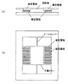
This embodiment is a third embodiment of the optical deflector according to the present invention. FIG. 4 shows the configuration. 4A is a configuration diagram of the movable part viewed from the surface opposite to the reflecting surface of the optical deflector, FIG. 4B is a cross-sectional view along AA ′, and FIG. 4C is BB ′. It is sectional drawing. Also in this embodiment, the movable mirror 1 is supported on the gimbal 3 by the two
さらに、本実施例においても、ジンバル3は2つのトーションバー4により可動ミラー1の回転軸と直交する軸方向にねじり回転可能にフレーム5に支持されている。そして、可動ミラー1、トーションバー2、ジンバル3、トーションバー4、およびフレーム5は、厚さ150μmのシリコン基板をエッチング加工することにより一体形成される。また、上記実施例と同様に、ジンバル3には2つの可動櫛型電極6が形成され、可動櫛型電極6と隙間を隔てて互いに噛み合うように2つの固定櫛型電極7が配置されている。フレーム5はスペーサ10を介して共通基板9に接合される。
Furthermore, also in this embodiment, the gimbal 3 is supported by the frame 5 by two torsion bars 4 so as to be torsionally rotated in the axial direction orthogonal to the rotation axis of the movable mirror 1. The movable mirror 1, the
本実施例では、共通基板9の表面に設けた複数の凹部25に、2つの固定櫛型電極7と3つの固定磁石32とが設置されている。2つの固定櫛型電極7は取り出し電極8を介して凹部25に配置されている。また、3つの固定磁石32は接着剤により凹部25に固定されている。本実施例の凹部25は高密度プラズマを用いたドライエッチングにより形成した。
In this embodiment, two fixed comb electrodes 7 and three fixed magnets 32 are installed in a plurality of
3つの固定磁石32はいずれもFeとCrとCoを含有する円筒状の永久磁石であり、長手方向に着磁されている。また、中央の固定磁石32と両脇の固定磁石32とは互いに逆方向に着磁されており、可動ミラー1を駆動させる磁場が可動コイル31に対して効果的に作用する配置となっている。ただし、固定磁石の数、着磁方向、配置形態はこれに限らず、磁場が可動コイル31に対して効果的に作用する態様であれば、どの様なものでもよい。また、3つの固定磁石32は、図4(a)のようにジンバル3を支持するトーションバー4の伸長方向と平行な方向に一列に配置されている。これにより、ジンバル3の揺動範囲が3つの固定磁石32の存在で制限されず、ジンバル3の偏向角を大きく取れる構造となっている。更に、3つの固定磁石32は、可動コイル31を支持するトーションバー2の伸長方向と直角な方向に配置されているが、3つが図4(c)に示すごとく空間を開けて離散的に配置されているので可動ミラー1が揺動する際にその端部が固定磁石32に触れる恐れは無く、可動ミラー1の偏向角も大きく取れる構造となっている。
All of the three fixed magnets 32 are cylindrical permanent magnets containing Fe, Cr, and Co, and are magnetized in the longitudinal direction. Further, the fixed magnet 32 at the center and the fixed magnets 32 on both sides are magnetized in opposite directions, and the magnetic field for driving the movable mirror 1 is arranged to effectively act on the
本実施例による光偏向器は、さらに、可動櫛型電極6と固定櫛型電極7との間に電位差を発生させ、可動櫛型電極6と固定櫛型電極7との間に働く静電力によりジンバル3を駆動させる静電駆動手段(不図示)と、可動コイル31に電流を流すことで発生する磁場が固定磁石32と作用することにより、可動ミラー1を駆動させる電磁駆動手段(不図示)とを有している。
The optical deflector according to the present embodiment further generates a potential difference between the
本実施例の駆動方法を説明する。本実施例においては、可動ミラー1を共振駆動により駆動し、ジンバル3をノコギリ波駆動信号を用いたDC制御により駆動する。まず、ジンバル3の駆動方法について説明すると、駆動電源と制御回路よりなる静電駆動手段により、可動櫛型電極6と固定櫛型電極7との間に60Hzのノコギリ波を印加して、ジンバル3を±10°の偏向角範囲で偏向させる。
A driving method of this embodiment will be described. In this embodiment, the movable mirror 1 is driven by resonance driving, and the gimbal 3 is driven by DC control using a sawtooth wave driving signal. First, a driving method of the gimbal 3 will be described. By applying electrostatic sawing means composed of a driving power source and a control circuit, a sawtooth wave of 60 Hz is applied between the
本実施例では、ジンバル3の外形寸法は4×10mm、厚さは150μmとする。また、トーションバー4の長さは4mm、幅は130μm(上記実施例のものより相当大きくなっている)、厚さは150μmである。ジンバル3の共振周波数は600Hz、トーションバー4のばね定数は1.5×10⁻³[Nm]であって、ジンバル3を±10°偏向させるために必要なトルクは2.5×10⁻⁴[Nm]である。ここにおいて必要とされる電圧は約1.2kVであった。本実施例においては、上記の様に、ジンバル3の駆動に共振駆動でなくノコギリ波によるDC駆動を用いる。DC駆動では駆動電圧が比較的高くなる欠点はあるが、画像形成において画像データを並べ替える必要が無い点で、1フレーム分のメモリが必要な往復利用の共振駆動と比較して有利である。 In this embodiment, the outer dimensions of the gimbal 3 are 4 × 10 mm and the thickness is 150 μm. The torsion bar 4 has a length of 4 mm, a width of 130 μm (which is considerably larger than that of the above embodiment), and a thickness of 150 μm. The resonance frequency of the gimbal 3 is 600 Hz, the spring constant of the torsion bar 4 is 1.5 × 10 −3 [Nm], and the torque required to deflect the gimbal 3 ± 10 ° is 2.5 × 10 −4. [Nm]. The required voltage here was about 1.2 kV. In the present embodiment, as described above, the driving of the gimbal 3 is not resonant driving but DC driving using a sawtooth wave. Although DC driving has a drawback that the driving voltage is relatively high, it is advantageous in comparison with reciprocal resonance driving that requires memory for one frame in that image data need not be rearranged in image formation.
次に、可動ミラー1の駆動方法について説明する。駆動電源と制御回路よりなる電磁駆動手段を用いて、可動コイル31に可動ミラー1のねじり振動周波数と同じ周波数の交流電流を流すことにより交流磁界を発生させ、この磁界と3つの固定磁石32との作用により可動ミラー1を電磁駆動させる。
Next, a method for driving the movable mirror 1 will be described. An electromagnetic field is generated by passing an alternating current having the same frequency as the torsional vibration frequency of the movable mirror 1 through the
本実施例では、可動ミラー1の外形寸法は1.1×1.3mm、厚さは150μm、慣性モーメントIは7×10⁻¹⁴ [kgm2]とする。トーションバー2の長さは3.7mm、幅は100μm、厚さは150μmである。また、可動ミラー1の共振周波数は20kHzで、偏向角は±12°である。さらに、可動コイル31の配線幅は30μm、厚さは1μm、ターン数は10ターンである。この場合、共振のQ値は約3000であり、駆動に必要な電圧は約10Vであった。
In the present embodiment, the outer dimensions of the movable mirror 1 are 1.1 × 1.3 mm, the thickness is 150 μm, and the moment of inertia I is 7 × 10 −14 [kgm 2 ]. The
上記構成の本実施例では、ジンバル3の回転軸伸長方向と平行な方向に固定磁石32を一列に配置することにより、ジンバル3の偏向角を妨げずに可動ミラー1の偏向を行なえた。また、凹部25を形成してそこに固定磁石32を納めることで固定磁石32の長さを大きくすることができ、磁場発生力を大きくできた。
In the present embodiment having the above-described configuration, the movable mirror 1 can be deflected without hindering the deflection angle of the gimbal 3 by arranging the fixed magnets 32 in a row in a direction parallel to the direction in which the rotation axis of the gimbal 3 extends. Moreover, the length of the fixed magnet 32 can be increased by forming the
(実施例4)
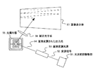
本実施例は、本発明による光偏向器を用いた画像形成装置の例である。図5に本実施例の構成を示す。まず、光源変調駆動部51から出た変調信号52により直接変調光源53の変調を行う。本実施例においては、直接変調光源53として赤色の半導体レーザを用いた。直接変調光源53は、また、赤色、青色、緑色の直接変調可能な光源を用い、これらを混色光学系にて混色して用いてもよい。直接変調光源53から直接変調された出力光54は、光偏向器55の反射面に照射される。さらに、光偏向器55により2次元的に偏向された反射光は、補正光学系56を通って画像表示体57上に画像として表示される。補正光学系56は、投影による画像の歪みを補正する光学系である。
Example 4
The present embodiment is an example of an image forming apparatus using an optical deflector according to the present invention. FIG. 5 shows the configuration of this embodiment. First, the modulation light source 53 is directly modulated by the modulation signal 52 output from the light source modulation drive unit 51. In this embodiment, a red semiconductor laser is used as the direct modulation light source 53. The direct modulation light source 53 may be a red, blue, or green light source that can be directly modulated, and these may be mixed by a color mixing optical system. The output light 54 directly modulated from the direct modulation light source 53 is applied to the reflection surface of the optical deflector 55. Further, the reflected light deflected two-dimensionally by the optical deflector 55 is displayed as an image on the image display body 57 through the correction optical system 56. The correction optical system 56 is an optical system that corrects image distortion due to projection.
本実施例の光偏向器55は、両方向において共振駆動である実施例2による光偏向器であり、光偏向器55を用いて出力光54をラスタ走査することにより、画像表示体57に画像を表示する。高速走査(可動ミラー)は、周波数20kHzの往復描画であり、偏向角は±10°で、反射角にすると±20°である。低速走査(ジンバル)は、30Hzの往復描画であり、偏向角は±8°で、反射角にすると±16°である。また、光偏向器55の駆動電圧は8Vである。 The optical deflector 55 of the present embodiment is an optical deflector according to the second embodiment that is resonantly driven in both directions. By raster scanning the output light 54 using the optical deflector 55, an image is displayed on the image display body 57. indicate. The high-speed scanning (movable mirror) is a reciprocal drawing with a frequency of 20 kHz, the deflection angle is ± 10 °, and the reflection angle is ± 20 °. The low-speed scanning (gimbal) is a reciprocal drawing of 30 Hz, the deflection angle is ± 8 °, and the reflection angle is ± 16 °. The drive voltage of the optical deflector 55 is 8V.
上記構成の本実施例により、コンパクトな構成を有し、比較的低電圧で駆動でき、偏向角が大きく、高精細な画像が得られる画像形成装置を実現することができた。 According to the present embodiment having the above-described configuration, an image forming apparatus that has a compact configuration, can be driven at a relatively low voltage, has a large deflection angle, and can obtain a high-definition image can be realized.
1 可動ミラー
2、4 トーションバー
3 ジンバル
5 フレーム
6 可動櫛型電極
7 固定櫛型電極
8 固定櫛型電極の取り出し電極
9 共通基板
10 スペーサ
11 反射膜
20 可動磁石
21 固定コイル
22 コイル基板
23 固定コイルの取り出し電極
25 凹部
31 可動コイル
32 固定磁石
33 電極パッド
51 光源変調駆動部
52 変調信号
53 直接変調光源
54 直接変調された出力光
55 光偏向器
56 補正光学系
57 画像表示体
DESCRIPTION OF SYMBOLS 1
Claims (9)
Priority Applications (2)
| Application Number | Priority Date | Filing Date | Title |
|---|---|---|---|
| JP2003415786A JP2005173411A (en) | 2003-12-12 | 2003-12-12 | Light deflector |
| US11/003,455 US7220009B2 (en) | 2003-12-12 | 2004-12-06 | Optical deflector |
Applications Claiming Priority (1)
| Application Number | Priority Date | Filing Date | Title |
|---|---|---|---|
| JP2003415786A JP2005173411A (en) | 2003-12-12 | 2003-12-12 | Light deflector |
Publications (2)
| Publication Number | Publication Date |
|---|---|
| JP2005173411A true JP2005173411A (en) | 2005-06-30 |
| JP2005173411A5 JP2005173411A5 (en) | 2007-01-25 |
Family
ID=34650592
Family Applications (1)
| Application Number | Title | Priority Date | Filing Date |
|---|---|---|---|
| JP2003415786A Pending JP2005173411A (en) | 2003-12-12 | 2003-12-12 | Light deflector |
Country Status (2)
| Country | Link |
|---|---|
| US (1) | US7220009B2 (en) |
| JP (1) | JP2005173411A (en) |
Cited By (9)
| Publication number | Priority date | Publication date | Assignee | Title |
|---|---|---|---|---|
| JP2006224224A (en) * | 2005-02-16 | 2006-08-31 | Fujitsu Ltd | Micro-oscillating element and its manufacturing method |
| JP2007212262A (en) * | 2006-02-09 | 2007-08-23 | Canon Inc | Rocking body device, potential measuring device, and optical deflection device |
| JP2008191513A (en) * | 2007-02-06 | 2008-08-21 | Seiko Epson Corp | Actuator, optical scanner, and image forming apparatus |
| WO2009119568A1 (en) * | 2008-03-25 | 2009-10-01 | 日本ビクター株式会社 | Two-dimensional optical beam deflector and image display device using the same |
| JP2010011547A (en) * | 2008-06-24 | 2010-01-14 | Panasonic Electric Works Co Ltd | Power generation device |
| JP2011242799A (en) * | 2011-07-28 | 2011-12-01 | Seiko Epson Corp | Image display device |
| JP2012252265A (en) * | 2011-06-06 | 2012-12-20 | Jvc Kenwood Corp | Optical scanner |
| JP2019104098A (en) * | 2017-12-14 | 2019-06-27 | 三菱電機株式会社 | Minute electronic mechanical device and inspection method thereof, acceleration sensor and movable mirror device |
| JP2021177214A (en) * | 2020-05-08 | 2021-11-11 | 三菱電機株式会社 | Optical scanner, and method for adjusting optical scanner |
Families Citing this family (26)
| Publication number | Priority date | Publication date | Assignee | Title |
|---|---|---|---|---|
| JP4027359B2 (en) * | 2003-12-25 | 2007-12-26 | キヤノン株式会社 | Micro oscillator, optical deflector, image forming device |
| JP4574396B2 (en) * | 2005-03-02 | 2010-11-04 | キヤノン株式会社 | Optical deflector |
| US7312915B2 (en) * | 2005-05-23 | 2007-12-25 | Texas Instruments Incorporated | Microelectromechanical devices with low inertia movable elements |
| JP4484778B2 (en) * | 2005-07-08 | 2010-06-16 | 富士フイルム株式会社 | Small thin film movable element, small thin film movable element array, and driving method of small thin film movable element |
| US7817318B2 (en) * | 2005-12-09 | 2010-10-19 | Canon Kabushiki Kaisha | Oscillating system and optical deflector |
| KR100718143B1 (en) * | 2005-12-15 | 2007-05-14 | 삼성전자주식회사 | 2-axis actuating scanner |
| US7978388B2 (en) * | 2006-01-12 | 2011-07-12 | Nippon Telegraph And Telephone Corporation | Mirror device and mirror device manufacturing method incorporating a collision preventive structure |
| JP5151065B2 (en) * | 2006-05-19 | 2013-02-27 | コニカミノルタホールディングス株式会社 | Optical scanner and scanning projector |
| JP2007316443A (en) * | 2006-05-26 | 2007-12-06 | Canon Inc | Light deflector and optical equipment using the same |
| US7593934B2 (en) * | 2006-07-28 | 2009-09-22 | Microsoft Corporation | Learning a document ranking using a loss function with a rank pair or a query parameter |
| WO2008068735A2 (en) * | 2006-12-03 | 2008-06-12 | Maradin Technologies Ltd. | A gimbaled scanning micro-mirror actuation scheme and architecture |
| JP2008191537A (en) * | 2007-02-07 | 2008-08-21 | Canon Inc | Vibrating element and light deflector equipped with the same |
| JP2009042737A (en) * | 2007-07-13 | 2009-02-26 | Canon Inc | Oscillating body apparatus and optical deflector using the same |
| JP2009025617A (en) * | 2007-07-20 | 2009-02-05 | Canon Inc | Oscillation body apparatus, optical deflector and optical apparatus using the same |
| JP2009122383A (en) * | 2007-11-14 | 2009-06-04 | Canon Inc | Method for manufacturing oscillator device, and optical deflector and optical device comprising oscillator device manufactured by this method |
| JP2009128463A (en) | 2007-11-21 | 2009-06-11 | Canon Inc | Method of manufacturing oscillating body apparatus, optical deflector composed of oscillating body apparatus manufactured by the method and optical equipment |
| JP2009163198A (en) * | 2007-12-10 | 2009-07-23 | Canon Inc | Method for manufacturing oscillator device, optical deflector, and image forming device |
| WO2009147654A1 (en) * | 2008-06-02 | 2009-12-10 | Maradin Technologies Ltd. | Gimbaled scanning micro-mirror apparatus |
| DE102009000599B4 (en) * | 2009-02-04 | 2021-03-18 | Robert Bosch Gmbh | Electrostatic drive, method for operating a micromechanical component with an electrostatic drive and manufacturing method for an electrostatic drive |
| JP5335654B2 (en) | 2009-12-04 | 2013-11-06 | キヤノン株式会社 | Mode conversion element |
| JP2013102060A (en) | 2011-11-09 | 2013-05-23 | Canon Inc | Charged particle optical system, and drawing device using the same |
| CN102963857B (en) * | 2012-10-17 | 2015-04-15 | 东南大学 | Micro electro mechanical (MEM) comb tooth mechanism capable of modulating backlash under electromagnetic drive |
| GB201312817D0 (en) * | 2012-11-29 | 2013-08-28 | Dann Engineering Ltd | Scanning apparatus |
| CN108347239B (en) * | 2018-05-04 | 2024-01-26 | 上海交通大学 | Electromagnetic drive bistable optical switch |
| US11909291B2 (en) * | 2018-06-26 | 2024-02-20 | Mitsumi Electric Co., Ltd. | Rotary reciprocating drive actuator with movable element and magnets and rotating mirror |
| EP3628964B1 (en) * | 2018-09-28 | 2024-02-14 | Hexagon Technology Center GmbH | Opto-electro-mechanical beam manipulation system |
Family Cites Families (21)
| Publication number | Priority date | Publication date | Assignee | Title |
|---|---|---|---|---|
| US4421381A (en) | 1980-04-04 | 1983-12-20 | Yokogawa Hokushin Electric Corp. | Mechanical vibrating element |
| US4317611A (en) | 1980-05-19 | 1982-03-02 | International Business Machines Corporation | Optical ray deflection apparatus |
| JPS6057052A (en) | 1983-09-05 | 1985-04-02 | Mitsubishi Electric Corp | Centrifugal stepless speed change device |
| JPS6057051A (en) | 1983-09-05 | 1985-04-02 | Mitsubishi Electric Corp | Centrifugal stepless speed change device |
| JPS6082711A (en) | 1983-10-13 | 1985-05-10 | Matsushita Electric Ind Co Ltd | Infrared ray burner |
| JPS60107017A (en) | 1983-11-16 | 1985-06-12 | Hitachi Ltd | Optical deflecting element |
| US6334573B1 (en) * | 1990-05-29 | 2002-01-01 | Symbol Technologies, Inc. | Integrated scanner on a common substrate having an omnidirectional mirror |
| JPH04343318A (en) | 1991-05-20 | 1992-11-30 | Fuji Electric Co Ltd | Torsional vibrator |
| US5819822A (en) * | 1996-03-29 | 1998-10-13 | Caterpillar Inc. | Fluid filler tool for a spin-on fluid filter |
| JPH10293134A (en) | 1997-02-19 | 1998-11-04 | Canon Inc | Optical detection or irradiation probe, near field optical microscope, recorder/placer and aligner employing it, and manufacture of probe |
| JPH11166935A (en) | 1997-09-25 | 1999-06-22 | Canon Inc | Light probe for light detection or irradiation, near-field optical microscope provided with the probe, manufacture of the light probe and substrate used for its manufacture |
| US6477132B1 (en) | 1998-08-19 | 2002-11-05 | Canon Kabushiki Kaisha | Probe and information recording/reproduction apparatus using the same |
| JP3554233B2 (en) | 1998-10-28 | 2004-08-18 | キヤノン株式会社 | Optical probe manufacturing method |
| US6327087B1 (en) | 1998-12-09 | 2001-12-04 | Canon Kabushiki Kaisha | Optical-thin-film material, process for its production, and optical device making use of the optical-thin-film material |
| US6436265B1 (en) | 1999-03-29 | 2002-08-20 | Canon Kabushiki Kaisha | Microstructure array, and apparatus and method for forming the microstructure array, and a mold for fabricating a microstructure array |
| JP3513448B2 (en) | 1999-11-11 | 2004-03-31 | キヤノン株式会社 | Optical probe |
| US6330102B1 (en) | 2000-03-24 | 2001-12-11 | Onix Microsystems | Apparatus and method for 2-dimensional steered-beam NxM optical switch using single-axis mirror arrays and relay optics |
| JP2003015064A (en) * | 2001-07-04 | 2003-01-15 | Fujitsu Ltd | Micro mirror element |
| JP3970066B2 (en) * | 2002-03-18 | 2007-09-05 | オリンパス株式会社 | Optical deflector and electromagnetic actuator |
| JP3862623B2 (en) | 2002-07-05 | 2006-12-27 | キヤノン株式会社 | Optical deflector and manufacturing method thereof |
| JP2005173436A (en) | 2003-12-15 | 2005-06-30 | Canon Inc | Optical deflector |
-
2003
- 2003-12-12 JP JP2003415786A patent/JP2005173411A/en active Pending
-
2004
- 2004-12-06 US US11/003,455 patent/US7220009B2/en not_active Expired - Fee Related
Cited By (11)
| Publication number | Priority date | Publication date | Assignee | Title |
|---|---|---|---|---|
| JP2006224224A (en) * | 2005-02-16 | 2006-08-31 | Fujitsu Ltd | Micro-oscillating element and its manufacturing method |
| JP4573664B2 (en) * | 2005-02-16 | 2010-11-04 | 富士通株式会社 | Micro oscillating device and manufacturing method thereof |
| US8142670B2 (en) | 2005-02-16 | 2012-03-27 | Fujitsu Limited | Micro-oscillating element and method of making the same |
| JP2007212262A (en) * | 2006-02-09 | 2007-08-23 | Canon Inc | Rocking body device, potential measuring device, and optical deflection device |
| JP2008191513A (en) * | 2007-02-06 | 2008-08-21 | Seiko Epson Corp | Actuator, optical scanner, and image forming apparatus |
| WO2009119568A1 (en) * | 2008-03-25 | 2009-10-01 | 日本ビクター株式会社 | Two-dimensional optical beam deflector and image display device using the same |
| JP2010011547A (en) * | 2008-06-24 | 2010-01-14 | Panasonic Electric Works Co Ltd | Power generation device |
| JP2012252265A (en) * | 2011-06-06 | 2012-12-20 | Jvc Kenwood Corp | Optical scanner |
| JP2011242799A (en) * | 2011-07-28 | 2011-12-01 | Seiko Epson Corp | Image display device |
| JP2019104098A (en) * | 2017-12-14 | 2019-06-27 | 三菱電機株式会社 | Minute electronic mechanical device and inspection method thereof, acceleration sensor and movable mirror device |
| JP2021177214A (en) * | 2020-05-08 | 2021-11-11 | 三菱電機株式会社 | Optical scanner, and method for adjusting optical scanner |
Also Published As
| Publication number | Publication date |
|---|---|
| US7220009B2 (en) | 2007-05-22 |
| US20050128609A1 (en) | 2005-06-16 |
Similar Documents
| Publication | Publication Date | Title |
|---|---|---|
| JP2005173411A (en) | Light deflector | |
| JP4928301B2 (en) | Oscillator device, driving method thereof, optical deflector, and image display device using optical deflector | |
| JP4092283B2 (en) | Two-dimensional optical scanner and optical device | |
| WO2012070610A1 (en) | Optical scanning device | |
| US9293975B2 (en) | Actuator, optical scanner, and image forming apparatus | |
| US8988750B2 (en) | Optical scanner, mirror chip, method of manufacturing optical scanner, and image forming apparatus | |
| CN109521561A (en) | A kind of electromagnetism MEMS micromirror | |
| JP2015087444A (en) | Optical scanner, image display device, head-mounted display, and head-up display | |
| CN100380172C (en) | Electromagnetic scanning micro-mirror and optical scanning device using the same | |
| JP2006115683A (en) | Electrostatic actuator and optical scanning device | |
| JP2005169553A (en) | Micro-actuator | |
| JP2003195204A (en) | Light deflector and light deflector array | |
| JP2008122622A (en) | Optical device, optical scanner, and image forming apparatus | |
| JP2005250078A (en) | Optical deflector | |
| JP5092406B2 (en) | Actuator, optical scanner and image forming apparatus | |
| JP6579241B2 (en) | Optical scanner and head mounted display | |
| JP7546752B2 (en) | Actuator | |
| JP4446345B2 (en) | Optical deflection element, optical deflector, optical scanning device, and image forming apparatus | |
| WO2024062856A1 (en) | Micromirror device and optical scanning apparatus | |
| JP4448425B2 (en) | Small imaging device | |
| JP2011100074A (en) | Optical device, optical scanner and image forming apparatus | |
| JP2022162810A (en) | Micromirror device and optical scanner | |
| KR20080067064A (en) | Scanning micromirror | |
| JP2006145962A (en) | Two-dimensional optical deflector and optical apparatus using same | |
| JP2006133387A (en) | Rocking body apparatus and method of manufacturing same |
Legal Events
| Date | Code | Title | Description |
|---|---|---|---|
| A521 | Written amendment |
Free format text: JAPANESE INTERMEDIATE CODE: A523 Effective date: 20061127 |
|
| A621 | Written request for application examination |
Free format text: JAPANESE INTERMEDIATE CODE: A621 Effective date: 20061127 |
|
| A977 | Report on retrieval |
Free format text: JAPANESE INTERMEDIATE CODE: A971007 Effective date: 20080526 |
|
| A131 | Notification of reasons for refusal |
Free format text: JAPANESE INTERMEDIATE CODE: A131 Effective date: 20080528 |
|
| A521 | Written amendment |
Free format text: JAPANESE INTERMEDIATE CODE: A523 Effective date: 20080722 |
|
| A02 | Decision of refusal |
Free format text: JAPANESE INTERMEDIATE CODE: A02 Effective date: 20080819 |