JP5178088B2 - Organic light emitting device - Google Patents
Organic light emitting device Download PDFInfo
- Publication number
- JP5178088B2 JP5178088B2 JP2007213393A JP2007213393A JP5178088B2 JP 5178088 B2 JP5178088 B2 JP 5178088B2 JP 2007213393 A JP2007213393 A JP 2007213393A JP 2007213393 A JP2007213393 A JP 2007213393A JP 5178088 B2 JP5178088 B2 JP 5178088B2
- Authority
- JP
- Japan
- Prior art keywords
- organic
- semi
- layer
- emitting device
- electrode
- Prior art date
- Legal status (The legal status is an assumption and is not a legal conclusion. Google has not performed a legal analysis and makes no representation as to the accuracy of the status listed.)
- Expired - Fee Related
Links
- 0 C*C(C)[n]1c(cccc2)c2c2c1cccc2 Chemical compound C*C(C)[n]1c(cccc2)c2c2c1cccc2 0.000 description 4
- OZVXBXKVMMIGDV-UHFFFAOYSA-N Cc(cc1)ccc1-[n]1c(cccc2)c2c2c1cccc2 Chemical compound Cc(cc1)ccc1-[n]1c(cccc2)c2c2c1cccc2 OZVXBXKVMMIGDV-UHFFFAOYSA-N 0.000 description 1
Images


Classifications
-
- H—ELECTRICITY
- H10—SEMICONDUCTOR DEVICES; ELECTRIC SOLID-STATE DEVICES NOT OTHERWISE PROVIDED FOR
- H10K—ORGANIC ELECTRIC SOLID-STATE DEVICES
- H10K50/00—Organic light-emitting devices
- H10K50/80—Constructional details
- H10K50/85—Arrangements for extracting light from the devices
- H10K50/852—Arrangements for extracting light from the devices comprising a resonant cavity structure, e.g. Bragg reflector pair
-
- C—CHEMISTRY; METALLURGY
- C09—DYES; PAINTS; POLISHES; NATURAL RESINS; ADHESIVES; COMPOSITIONS NOT OTHERWISE PROVIDED FOR; APPLICATIONS OF MATERIALS NOT OTHERWISE PROVIDED FOR
- C09K—MATERIALS FOR MISCELLANEOUS APPLICATIONS, NOT PROVIDED FOR ELSEWHERE
- C09K11/00—Luminescent, e.g. electroluminescent, chemiluminescent materials
- C09K11/06—Luminescent, e.g. electroluminescent, chemiluminescent materials containing organic luminescent materials
-
- H—ELECTRICITY
- H05—ELECTRIC TECHNIQUES NOT OTHERWISE PROVIDED FOR
- H05B—ELECTRIC HEATING; ELECTRIC LIGHT SOURCES NOT OTHERWISE PROVIDED FOR; CIRCUIT ARRANGEMENTS FOR ELECTRIC LIGHT SOURCES, IN GENERAL
- H05B33/00—Electroluminescent light sources
- H05B33/12—Light sources with substantially two-dimensional radiating surfaces
- H05B33/14—Light sources with substantially two-dimensional radiating surfaces characterised by the chemical or physical composition or the arrangement of the electroluminescent material, or by the simultaneous addition of the electroluminescent material in or onto the light source
-
- H—ELECTRICITY
- H05—ELECTRIC TECHNIQUES NOT OTHERWISE PROVIDED FOR
- H05B—ELECTRIC HEATING; ELECTRIC LIGHT SOURCES NOT OTHERWISE PROVIDED FOR; CIRCUIT ARRANGEMENTS FOR ELECTRIC LIGHT SOURCES, IN GENERAL
- H05B33/00—Electroluminescent light sources
- H05B33/12—Light sources with substantially two-dimensional radiating surfaces
- H05B33/22—Light sources with substantially two-dimensional radiating surfaces characterised by the chemical or physical composition or the arrangement of auxiliary dielectric or reflective layers
-
- H—ELECTRICITY
- H10—SEMICONDUCTOR DEVICES; ELECTRIC SOLID-STATE DEVICES NOT OTHERWISE PROVIDED FOR
- H10K—ORGANIC ELECTRIC SOLID-STATE DEVICES
- H10K59/00—Integrated devices, or assemblies of multiple devices, comprising at least one organic light-emitting element covered by group H10K50/00
- H10K59/30—Devices specially adapted for multicolour light emission
- H10K59/35—Devices specially adapted for multicolour light emission comprising red-green-blue [RGB] subpixels
-
- C—CHEMISTRY; METALLURGY
- C09—DYES; PAINTS; POLISHES; NATURAL RESINS; ADHESIVES; COMPOSITIONS NOT OTHERWISE PROVIDED FOR; APPLICATIONS OF MATERIALS NOT OTHERWISE PROVIDED FOR
- C09K—MATERIALS FOR MISCELLANEOUS APPLICATIONS, NOT PROVIDED FOR ELSEWHERE
- C09K2211/00—Chemical nature of organic luminescent or tenebrescent compounds
- C09K2211/10—Non-macromolecular compounds
- C09K2211/1003—Carbocyclic compounds
- C09K2211/1011—Condensed systems
-
- C—CHEMISTRY; METALLURGY
- C09—DYES; PAINTS; POLISHES; NATURAL RESINS; ADHESIVES; COMPOSITIONS NOT OTHERWISE PROVIDED FOR; APPLICATIONS OF MATERIALS NOT OTHERWISE PROVIDED FOR
- C09K—MATERIALS FOR MISCELLANEOUS APPLICATIONS, NOT PROVIDED FOR ELSEWHERE
- C09K2211/00—Chemical nature of organic luminescent or tenebrescent compounds
- C09K2211/10—Non-macromolecular compounds
- C09K2211/1003—Carbocyclic compounds
- C09K2211/1014—Carbocyclic compounds bridged by heteroatoms, e.g. N, P, Si or B
-
- C—CHEMISTRY; METALLURGY
- C09—DYES; PAINTS; POLISHES; NATURAL RESINS; ADHESIVES; COMPOSITIONS NOT OTHERWISE PROVIDED FOR; APPLICATIONS OF MATERIALS NOT OTHERWISE PROVIDED FOR
- C09K—MATERIALS FOR MISCELLANEOUS APPLICATIONS, NOT PROVIDED FOR ELSEWHERE
- C09K2211/00—Chemical nature of organic luminescent or tenebrescent compounds
- C09K2211/10—Non-macromolecular compounds
- C09K2211/1018—Heterocyclic compounds
- C09K2211/1025—Heterocyclic compounds characterised by ligands
- C09K2211/1029—Heterocyclic compounds characterised by ligands containing one nitrogen atom as the heteroatom
- C09K2211/1033—Heterocyclic compounds characterised by ligands containing one nitrogen atom as the heteroatom with oxygen
-
- C—CHEMISTRY; METALLURGY
- C09—DYES; PAINTS; POLISHES; NATURAL RESINS; ADHESIVES; COMPOSITIONS NOT OTHERWISE PROVIDED FOR; APPLICATIONS OF MATERIALS NOT OTHERWISE PROVIDED FOR
- C09K—MATERIALS FOR MISCELLANEOUS APPLICATIONS, NOT PROVIDED FOR ELSEWHERE
- C09K2211/00—Chemical nature of organic luminescent or tenebrescent compounds
- C09K2211/10—Non-macromolecular compounds
- C09K2211/1018—Heterocyclic compounds
- C09K2211/1025—Heterocyclic compounds characterised by ligands
- C09K2211/1029—Heterocyclic compounds characterised by ligands containing one nitrogen atom as the heteroatom
- C09K2211/1037—Heterocyclic compounds characterised by ligands containing one nitrogen atom as the heteroatom with sulfur
-
- C—CHEMISTRY; METALLURGY
- C09—DYES; PAINTS; POLISHES; NATURAL RESINS; ADHESIVES; COMPOSITIONS NOT OTHERWISE PROVIDED FOR; APPLICATIONS OF MATERIALS NOT OTHERWISE PROVIDED FOR
- C09K—MATERIALS FOR MISCELLANEOUS APPLICATIONS, NOT PROVIDED FOR ELSEWHERE
- C09K2211/00—Chemical nature of organic luminescent or tenebrescent compounds
- C09K2211/10—Non-macromolecular compounds
- C09K2211/1018—Heterocyclic compounds
- C09K2211/1025—Heterocyclic compounds characterised by ligands
- C09K2211/1088—Heterocyclic compounds characterised by ligands containing oxygen as the only heteroatom
-
- H—ELECTRICITY
- H10—SEMICONDUCTOR DEVICES; ELECTRIC SOLID-STATE DEVICES NOT OTHERWISE PROVIDED FOR
- H10K—ORGANIC ELECTRIC SOLID-STATE DEVICES
- H10K2102/00—Constructional details relating to the organic devices covered by this subclass
- H10K2102/301—Details of OLEDs
- H10K2102/302—Details of OLEDs of OLED structures
- H10K2102/3023—Direction of light emission
- H10K2102/3026—Top emission
-
- H—ELECTRICITY
- H10—SEMICONDUCTOR DEVICES; ELECTRIC SOLID-STATE DEVICES NOT OTHERWISE PROVIDED FOR
- H10K—ORGANIC ELECTRIC SOLID-STATE DEVICES
- H10K2102/00—Constructional details relating to the organic devices covered by this subclass
- H10K2102/301—Details of OLEDs
- H10K2102/351—Thickness
-
- H—ELECTRICITY
- H10—SEMICONDUCTOR DEVICES; ELECTRIC SOLID-STATE DEVICES NOT OTHERWISE PROVIDED FOR
- H10K—ORGANIC ELECTRIC SOLID-STATE DEVICES
- H10K50/00—Organic light-emitting devices
- H10K50/80—Constructional details
- H10K50/805—Electrodes
- H10K50/82—Cathodes
- H10K50/828—Transparent cathodes, e.g. comprising thin metal layers
Landscapes
- Chemical & Material Sciences (AREA)
- Engineering & Computer Science (AREA)
- Materials Engineering (AREA)
- Organic Chemistry (AREA)
- Physics & Mathematics (AREA)
- Optics & Photonics (AREA)
- Electroluminescent Light Sources (AREA)
- Devices For Indicating Variable Information By Combining Individual Elements (AREA)
Description
本発明は、発光色が異なる有機EL素子を複数備える有機発光装置に関する。 The present invention relates to an organic light emitting device including a plurality of organic EL elements having different emission colors.
有機EL素子(有機発光素子、有機エレクトロルミネッセンス素子)が現在盛んに研究開発されている。有機EL素子の課題として色純度の確保と発光効率の向上がある。この課題の解決策の1つとして、光取り出し側の電極を半透過にすることで、両電極間で発光層から射出される光を共振させる共振器構造が知られている。 Organic EL elements (organic light-emitting elements and organic electroluminescence elements) are currently being actively researched and developed. As problems of the organic EL element, there are securing of color purity and improvement of luminous efficiency. As one solution to this problem, there is known a resonator structure in which light emitted from a light emitting layer is resonated between both electrodes by making the light extraction side electrode semi-transmissive.
例えば、特許文献1は、光反射材料からなる第1電極と、透明電極からなる第2電極との間に発光層を挟持し、第2電極及び発光層の少なくとも一方が発光層で発光した光を共振させる共振部を有する表示素子を開示している。この素子は、下記<式2>を満たす範囲で、共振部の光学的距離Lが正の最小値となるように構成されている。 For example, in Patent Document 1, a light emitting layer is sandwiched between a first electrode made of a light reflecting material and a second electrode made of a transparent electrode, and at least one of the second electrode and the light emitting layer emits light emitted from the light emitting layer. The display element which has the resonance part which resonates is disclosed. This element is configured such that the optical distance L of the resonance part is a positive minimum value in a range satisfying the following <Expression 2>.
<式2>
(2L)/λ+Φ/(2π)=m (mは整数)
L:共振部の光学的距離
Φ:発光層で発生した光が共振部の両端で反射する際に生じる位相シフト
λ:発光層で発生した光のうちの取り出したい光のスペクトルのピーク波長
<Formula 2>
(2L) / λ + Φ / (2π) = m (m is an integer)
L: optical distance of the resonance part Φ: phase shift generated when light generated in the light emitting layer is reflected at both ends of the resonance part λ: peak wavelength of spectrum of light to be extracted from light generated in the light emitting layer
また、特許文献2は発光中心から各反射層までの光学的距離を規定することを開示している。 Patent Document 2 discloses that the optical distance from the light emission center to each reflective layer is defined.
半透過層(半透過電極)を複数の有機EL素子に同一膜厚で形成すると、材料の波長分散性により各有機EL素子で半透過層の透過率、反射率が異なるため、各有機EL素子で共振の強さが異なる。そのため、共振の強さが相対的に弱い有機EL素子では十分に発光効率を高めることができない課題がある。また、有機発光装置として視野角による色度ずれは大きな問題点であるが、共振が強いほど視野角ずれは大きくなる。 When a semi-transmissive layer (semi-transmissive electrode) is formed on a plurality of organic EL elements with the same film thickness, the transmissivity and reflectivity of the semi-transmissive layer differ depending on the wavelength dispersion of the material. The strength of resonance is different. Therefore, there is a problem that the organic EL element having a relatively low resonance intensity cannot sufficiently increase the light emission efficiency. Further, the chromaticity shift due to the viewing angle as an organic light emitting device is a big problem, but the viewing angle shift becomes larger as the resonance becomes stronger.
そこで本発明は、上記問題点に鑑みてなされたものであり、有機EL素子の視野角による色度ずれを抑えつつ共振を強め、全体的な発光効率の向上を達成することができる有機発光装置を提供することを目的とする。 Therefore, the present invention has been made in view of the above problems, and an organic light-emitting device capable of enhancing resonance and suppressing the chromaticity shift due to the viewing angle of the organic EL element, thereby achieving improvement in overall light emission efficiency. The purpose is to provide.
また本発明は、製造バラツキの少ない有機発光装置を提供することも目的とする。 Another object of the present invention is to provide an organic light-emitting device with little manufacturing variation.
上記背景技術の課題を解決するための手段として、請求項1に記載した発明に係る有機発光装置は、
赤色を発する有機EL素子と、緑色を発する有機EL素子と、青色を発する有機EL素子と、を備えており、
前記有機EL素子は、陽極と、陰極と、発光層を含む有機化合物層と、を有し、前記陽極及び前記陰極のうち光取り出し側の電極に金属膜からなる半透過電極を含み、前記陽極と前記陰極の間で前記発光層が発した光を共振させる共振器構造を有する有機発光装置において、
前記青色を発する有機EL素子の半透過電極である金属膜の膜厚が、他の色を発する有機EL素子の半透過電極である金属膜の膜厚よりも薄く、かつ視野角45度以内での正面との色度ずれが、
<式1>
Δu’v’<0.025
(但し、Δu’v’はu’v’色度図での正面視の色度座標と斜面視の色度座標との距離のことである。)
を満たすように設定されていることを特徴とする。
As means for solving the problems of the background art, an organic light-emitting device according to the invention described in claim 1 is:
An organic EL element that emits red, an organic EL element that emits green, and an organic EL element that emits blue;
The organic EL element includes an anode, a cathode, and an organic compound layer including a light emitting layer, and includes a transflective electrode made of a metal film as an electrode on a light extraction side of the anode and the cathode, and the anode In an organic light emitting device having a resonator structure that resonates light emitted from the light emitting layer between the cathode and the cathode,
The film thickness of the metal film that is the semi-transmissive electrode of the organic EL element that emits blue is thinner than the metal film that is the semi-transmissive electrode of the organic EL element that emits other colors, and the viewing angle is within 45 degrees. Chromaticity deviation from the front of
<Formula 1>
Δu′v ′ <0.025
(However, Δu′v ′ is the distance between the chromaticity coordinates of the front view and the chromaticity coordinates of the oblique view in the u′v ′ chromaticity diagram.)
It is set so that it may satisfy | fill.
本発明によれば、有機EL素子に最適な共振器構造を設けることができるため、視野角による色度ずれを抑えつつ共振を強め、全体的な発光効率の向上を達成することができる。 According to the present invention, since an optimal resonator structure can be provided for an organic EL element, resonance can be strengthened while suppressing a chromaticity shift due to a viewing angle, and an overall improvement in light emission efficiency can be achieved.
特に、全部又は一部の有機EL素子の半透過層の材料が異なる構成とすると、前記有機EL素子の両電極間の厚さを厚くすることができ、膜厚バラツキによるロバスト性が高まる。そのため、製造バラツキの少ない有機発光装置を提供することができる。 In particular, when the materials of the semi-transmissive layers of all or some of the organic EL elements are different, the thickness between both electrodes of the organic EL element can be increased, and the robustness due to film thickness variation is increased. Therefore, an organic light emitting device with little manufacturing variation can be provided.
共振器構造を有する有機EL素子において、両電極の間で発光層が発した光を特定の波長で共振させる場合、前記共振の強さは半透過層(半透過電極)の反射率、透過率に依存することが知られている。 In an organic EL device having a resonator structure, when the light emitted from the light emitting layer is resonated at a specific wavelength between the two electrodes, the strength of the resonance is the reflectance and transmittance of the semi-transmissive layer (semi-transmissive electrode). It is known to depend on
例えば、Applied Physics Letters 88,073517 (2006):
“High−efficiency microcavity top−emitting organic light−emitting diodes using silver anode”、では放射強度を示す式として下記の<数1>がある。
For example, Applied Physics Letters 88, 073517 (2006):
In “High-efficiency microcavity top-emitting organic light-emitting diodes using silver anode”, there is the following <Equation 1> as a formula indicating the radiation intensity.
![]()
![]()
ここでは反射面を有する第1電極(陽極)、半透過層を有する第2電極(陰極)の有機EL素子を考えており、R2、T2は半透過層の反射率、透過率である。R1は第1電極の反射率である。φ1、φ2は各電極での位相シフトである。zは発光位置と第1電極との間の距離であり、dは共振波長である。<数1>から分かる通り、半透過層の反射率、透過率の値によって放射強度、つまり、共振の強さが異なる。 Here, an organic EL element of a first electrode (anode) having a reflective surface and a second electrode (cathode) having a semi-transmissive layer is considered, and R 2 and T 2 are the reflectance and transmittance of the semi-transmissive layer. . R 1 is the reflectance of the first electrode. φ 1 and φ 2 are phase shifts at each electrode. z is a distance between the light emitting position and the first electrode, and d is a resonance wavelength. As can be seen from <Equation 1>, the intensity of the radiation, that is, the strength of resonance differs depending on the reflectance and transmittance of the semi-transmissive layer.
そのため、共振器構造を有する有機EL素子を複数備えた有機発光装置を考えた場合、各有機EL素子で共振の強さを調整することが最適である。本発明では、半透過層の材料及び膜厚、又は半透過層の材料若しくは膜厚を発光色に応じて最適化することで高効率な有機発光装置を得る。 Therefore, when considering an organic light-emitting device including a plurality of organic EL elements having a resonator structure, it is optimal to adjust the strength of resonance with each organic EL element. In the present invention, a highly efficient organic light-emitting device is obtained by optimizing the material and film thickness of the semi-transmissive layer, or the material or film thickness of the semi-transmissive layer according to the emission color.
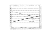
ここで、有機EL素子の発光効率と半透過層の膜厚との間には図3のような上に凸な関係が見受けられる。すなわち、半透過層の膜厚を厚くすると、反射率が上がるため発光効率が上がる。しかしながら、半透過層の膜厚を厚くしすぎると、前記半透過層上での吸収が大きくなるために発光効率は下がる。 Here, an upward convex relationship as shown in FIG. 3 is observed between the luminous efficiency of the organic EL element and the film thickness of the semi-transmissive layer. That is, when the film thickness of the semi-transmissive layer is increased, the light emission efficiency is increased because the reflectance is increased. However, if the thickness of the semi-transmissive layer is excessively increased, the light emission efficiency decreases because the absorption on the semi-transmissive layer increases.
発光効率の最大値を与える最適膜厚は半透過層の材料および発光波長によって異なるが、各色発光素子の相対比較では、発光波長が大きい有機EL素子ほどこの最適膜厚は厚くなる。 The optimum film thickness that gives the maximum value of the light emission efficiency varies depending on the material of the transflective layer and the light emission wavelength. However, in the relative comparison of the light emitting elements of each color, the organic EL element having a larger light emission wavelength becomes thicker.
但し、本発明者が検討した範囲内では、半透過層の光学定数をバルクの値としたときに、有機EL素子の共振の強さは<数1>に従うわけではなかった。半透過層の光学定数がバルクの値と異なる等の理由が考えられるが、本発明に支障をきたすわけではない。 However, within the range studied by the present inventors, when the optical constant of the semi-transmissive layer is a bulk value, the intensity of resonance of the organic EL element does not follow <Equation 1>. The reason is that the optical constant of the semi-transmissive layer is different from the bulk value, but this does not hinder the present invention.
<実施形態1>
図1は、本発明に係る有機発光装置の一構成例を示した概略部分拡大断面図である。
<Embodiment 1>
FIG. 1 is a schematic partial enlarged cross-sectional view showing one configuration example of an organic light-emitting device according to the present invention.
図示した有機発光装置10は、赤色(R)、緑色(G)、青色(B)の発光色を示す有機EL素子9R、9G、9Bからなる有機発光装置であり、全ての有機EL素子が共振器構造を有している。 The illustrated organic light-emitting device 10 is an organic light-emitting device composed of organic EL elements 9R, 9G, and 9B that exhibit red (R), green (G), and blue (B) emission colors, and all the organic EL elements resonate. It has a vessel structure.
各有機EL素子9R、9G、9Bは、基板1上に、陽極(アノード)として反射面を有する第1電極2、有機化合物層6としてホール輸送層3及び発光層4及び電子輸送層5を設けている。さらに陰極(カソード)としての積層構造である半透過層7及び透明導電層(透明電極)11、保護層8を設けた構成である。有機EL素子に電流を通電することで、陽極から注入されたホールと陰極から注入された電子とを、RGBそれぞれの発光層4において再結合させ、RGBそれぞれの光を陰極側から取り出すことが可能なトップエミッション型の構成とされている。 Each organic EL element 9R, 9G, 9B is provided with a first electrode 2 having a reflective surface as an anode (anode) on a substrate 1, a hole transport layer 3, a light emitting layer 4, and an electron transport layer 5 as an organic compound layer 6. ing. Further, a semi-transmissive layer 7, a transparent conductive layer (transparent electrode) 11, and a protective layer 8 having a laminated structure as a cathode (cathode) are provided. By supplying current to the organic EL element, holes injected from the anode and electrons injected from the cathode can be recombined in each of the RGB light-emitting layers 4 and each RGB light can be extracted from the cathode side. The top emission type configuration.
第1電極2は、正孔の注入を効率よく行うため、仕事関数が大きい材料が用いられる。具体的には、ITO又はIZOなどの透明性の導電性金属酸化物層2bからなり、その下に反射率の高いメタル層2a、例えば、クロム、銀、白金、アルミ、又はこれらを含む合金などを形成することが好ましい。メタル層2aが形成される場合、このメタル層2aと導電性金属酸化物層2bとの境界面が共振器構造の下部反射面に相当する。 The first electrode 2 is made of a material having a large work function in order to efficiently inject holes. Specifically, it is composed of a transparent conductive metal oxide layer 2b such as ITO or IZO, and a metal layer 2a having a high reflectance below it, for example, chromium, silver, platinum, aluminum, or an alloy containing these. Is preferably formed. When the metal layer 2a is formed, the interface between the metal layer 2a and the conductive metal oxide layer 2b corresponds to the lower reflection surface of the resonator structure.
半透過層7は、仕事関数の低い金属薄膜などが適している。具体例には、アルミニウム、カルシウム、マグネシウム、銀、金等の金属、又はこれら金属とリチウム金属等の合金、又はマグネシウムと銀の合金等が挙げられる。更にはそれらの合金がある。合金の場合、物理的劣化及び化学的劣化に対する耐性が高いため、半透過層の材料として好適である。 As the semi-transmissive layer 7, a metal thin film having a low work function is suitable. Specific examples include metals such as aluminum, calcium, magnesium, silver, and gold, alloys of these metals and lithium metals, alloys of magnesium and silver, and the like. Furthermore, there are those alloys. In the case of an alloy, since it has high resistance to physical deterioration and chemical deterioration, it is suitable as a material for a semi-transmissive layer.
本実施形態では、第1電極のメタル層2a及び第2電極の半透過層7は共に銀膜で形成されている。半透過層7の銀膜は、その膜厚を7Rで30nm、7Gで25nm、7Bで15nmとされている。つまり、発光波長の大きい有機EL素子ほど、半透過層の膜厚が厚い。各色有機EL素子で発光効率[cd/A]が最大になるように各有機EL素子で半透過層7の膜厚を変えている。 In the present embodiment, the metal layer 2a of the first electrode and the semi-transmissive layer 7 of the second electrode are both formed of a silver film. The silver film of the semi-transmissive layer 7 has a film thickness of 30 nm for 7R, 25 nm for 7G, and 15 nm for 7B. That is, the organic EL element having a larger emission wavelength has a thicker semi-transmissive layer. The thickness of the semi-transmissive layer 7 is changed in each organic EL element so that the luminous efficiency [cd / A] is maximized in each color organic EL element.
一対の電極2と7で挟持された有機化合物層を成すホール輸送層3、発光層4、電子輸送層5、(電子注入層(図示省略))としては、低分子材料で構成されても、高分子材料で構成されても、両者を用いて構成されてもよく、特に限定されるものではない。必要に応じてこれまで知られている材料を使用することができる。 The hole transport layer 3, the light emitting layer 4, the electron transport layer 5 (electron injection layer (not shown)) forming an organic compound layer sandwiched between the pair of electrodes 2 and 7 may be composed of a low molecular material, Even if it comprises a high molecular material, it may comprise using both, It does not specifically limit. Conventionally known materials can be used as required.
ホール輸送性材料としては、陽極からのホールの注入を容易にし、また注入されたホールを発光層4に輸送するに優れたモビリティを有することが好ましい。また、必要に応じて陽極2とホール輸送層3でホール注入層(図示省略)を挟持しても良い。ホール注入輸送性能を有する低分子及び高分子系材料としては、トリアリールアミン誘導体、フェニレンジアミン誘導体、トリアゾール誘導体、オキサジアゾール誘導体、イミダゾール誘導体、ピラゾリン誘導体、ピラゾロン誘導体、オキサゾール誘導体;
フルオレノン誘導体、ヒドラゾン誘導体、スチルベン誘導体、フタロシアニン誘導体、ポルフィリン誘導体、及びポリ(ビニルカルバゾール)、ポリ(シリレン)、ポリ(チオフェン)、その他導電性高分子が挙げられる。もちろんこれらに限定されるものではない。以下に、具体例の一部を示す。
The hole transporting material preferably has excellent mobility for facilitating the injection of holes from the anode and transporting the injected holes to the light emitting layer 4. Further, a hole injection layer (not shown) may be sandwiched between the anode 2 and the hole transport layer 3 as necessary. Examples of the low-molecular and high-molecular materials having hole injection and transport performance include triarylamine derivatives, phenylenediamine derivatives, triazole derivatives, oxadiazole derivatives, imidazole derivatives, pyrazoline derivatives, pyrazolone derivatives, oxazole derivatives;
Examples include fluorenone derivatives, hydrazone derivatives, stilbene derivatives, phthalocyanine derivatives, porphyrin derivatives, poly (vinyl carbazole), poly (silylene), poly (thiophene), and other conductive polymers. Of course, it is not limited to these. Some specific examples are shown below.

発光材料としては、発光効率の高い蛍光色素や燐光材料が用いられる。以下に具体例の一部を示す。 As the light emitting material, a fluorescent dye or a phosphorescent material having high light emission efficiency is used. Some specific examples are shown below.
電子輸送性材料としては、注入された電子を発光層4に輸送する機能を有するものから任意に選ぶことができ、ホール輸送材料のキャリア移動度とのバランス等を考慮し選択される。電子注入輸送性能を有する材料としては、オキサジアゾール誘導体、オキサゾール誘導体、チアゾール誘導体、チアジアゾール誘導体、ピラジン誘導体、トリアゾール誘導体、トリアジン誘導体、ペリレン誘導体、キノリン誘導体、キノキサリン誘導体;
フルオレノン誘導体、アントロン誘導体、フェナントロリン誘導体、有機金属錯体等が挙げられるが、もちろんこれらに限定されるものではない。以下に、具体例の一部を示す。
The electron transporting material can be arbitrarily selected from those having a function of transporting injected electrons to the light emitting layer 4, and is selected in consideration of the balance with the carrier mobility of the hole transporting material. Examples of materials having electron injection and transport performance include oxadiazole derivatives, oxazole derivatives, thiazole derivatives, thiadiazole derivatives, pyrazine derivatives, triazole derivatives, triazine derivatives, perylene derivatives, quinoline derivatives, and quinoxaline derivatives;
Examples include, but are not limited to, fluorenone derivatives, anthrone derivatives, phenanthroline derivatives, organometallic complexes, and the like. Some specific examples are shown below.
電子注入材料としては、前述した電子輸送性材料に、アルカリ金属やアルカリ土類金属、もしくはその化合物を0.1〜数十%含有させることにより、電子注入性を付与することができる。なお、電子注入層は、必要不可欠な層ではないが、この後に半透過層7を形成する際のダメージを考慮すると、良好な電子注入性を確保するために10〜100nm程度の膜厚で挿入した方が好ましい。 As the electron injecting material, electron injecting property can be imparted by adding 0.1 to several tens of percent of an alkali metal, an alkaline earth metal, or a compound thereof in the above-described electron transporting material. Although the electron injection layer is not an indispensable layer, it is inserted with a film thickness of about 10 to 100 nm in order to ensure good electron injection properties in consideration of damage when the semi-transmissive layer 7 is formed thereafter. Is preferable.
本発明の有機化合物層6は、一般には真空蒸着法、イオン化蒸着法、スパッタリング、プラズマあるいは、適当な溶媒に溶解させて公知の塗布法(例えば、スピンコーティング、ディッピング、キャスト法、LB法、インクジェット法等)により薄膜を形成する。特に塗布法で成膜する場合は、適当な結着樹脂と組み合わせて膜を形成することもできる。上記結着樹脂としては、広範囲な結着樹脂より選択でき、例えば、ポリビニルカルバゾール樹脂、ポリカーボネート樹脂、ポリエステル樹脂、ポリアリレート樹脂、ポリスチレン樹脂、ABS樹脂、ポリブタジエン樹脂、ポリウレタン樹脂、アクリル樹脂;
メタクリル樹脂、ブチラール樹脂、ポリビニルアセタール樹脂、ポリアミド樹脂、ポリイミド樹脂、ポリエチレン樹脂、ポリエーテルスルホン樹脂、ジアリルフタレート樹脂、フェノール樹脂、エポキシ樹脂、シリコン樹脂;
ポリスルホン樹脂、尿素樹脂等が挙げられるが、これらに限定されるものではない。また、これらは単独又は共重合体ポリマーとして1種又は2種以上混合しても良い。更に必要に応じて、公知の可塑剤、酸化防止剤、紫外線吸収剤等の添加剤を併用しても良い。
In general, the organic compound layer 6 of the present invention is dissolved in a vacuum deposition method, ionization deposition method, sputtering, plasma, or an appropriate solvent, and a known coating method (for example, spin coating, dipping, casting method, LB method, inkjet method). Method). In particular, when a film is formed by a coating method, the film can be formed in combination with an appropriate binder resin. The binder resin can be selected from a wide range of binder resins. For example, polyvinyl carbazole resin, polycarbonate resin, polyester resin, polyarylate resin, polystyrene resin, ABS resin, polybutadiene resin, polyurethane resin, acrylic resin;
Methacrylic resin, butyral resin, polyvinyl acetal resin, polyamide resin, polyimide resin, polyethylene resin, polyethersulfone resin, diallyl phthalate resin, phenol resin, epoxy resin, silicone resin;
Examples include, but are not limited to, polysulfone resins and urea resins. These may be used alone or in combination as a copolymer polymer. Furthermore, you may use together additives, such as a well-known plasticizer, antioxidant, and an ultraviolet absorber, as needed.
保護層8は、酸素や水分等との接触を防止する目的で設けられる。保護層8としては、窒化シリコン、窒化酸化シリコン等の金属窒化物膜や、酸化タンタル等の金属酸化物膜、ダイヤモンド薄膜が挙げられる。また、フッ素樹脂、ポリパラキシレン、ポリエチレン、シリコーン樹脂、ポリスチレン樹脂等の高分子膜、さらには、光硬化性樹脂等が挙げられる。また、ガラス、気体不透過性フィルム、金属などをカバーし、適当な封止樹脂により素子自体をパッケージングすることもできる。また、防湿性を高める為に、保護層8内に吸湿材を含有させても良い。 The protective layer 8 is provided for the purpose of preventing contact with oxygen or moisture. Examples of the protective layer 8 include metal nitride films such as silicon nitride and silicon nitride oxide, metal oxide films such as tantalum oxide, and diamond thin films. Moreover, polymer films, such as a fluororesin, polyparaxylene, polyethylene, a silicone resin, a polystyrene resin, Furthermore, photocurable resin etc. are mentioned. Further, it is possible to cover glass, a gas impermeable film, a metal, etc., and to package the element itself with an appropriate sealing resin. Further, a moisture absorbing material may be included in the protective layer 8 in order to improve moisture resistance.
<比較例1>
比較例1の有機発光装置は、半透過層の膜厚を全ての有機EL素子で同一とした構成であり、半透過層は膜厚15nmの銀膜とする。半透過層を除く有機EL素子の構成は実施形態1と同一とする。図2は比較例1の有機化合物層からの反射率、透過率である。但し、銀の光学定数にはバルクの値を用いた。
<Comparative Example 1>
The organic light emitting device of Comparative Example 1 has a configuration in which the thickness of the semi-transmissive layer is the same for all organic EL elements, and the semi-transmissive layer is a silver film having a thickness of 15 nm. The configuration of the organic EL element excluding the semi-transmissive layer is the same as that of the first embodiment. FIG. 2 shows the reflectance and transmittance from the organic compound layer of Comparative Example 1. However, the bulk value was used for the optical constant of silver.
全ての有機EL素子で半透過層の膜厚を一定にすると、波長によって反射率、透過率が異なることから、共振の強さが各有機EL素子で異なる。そのため、全ての有機EL素子で最適な共振構造にはなっていない。 If the film thickness of the semi-transmissive layer is constant in all the organic EL elements, the reflectance and the transmittance differ depending on the wavelength, and therefore the resonance intensity differs for each organic EL element. Therefore, not all organic EL elements have an optimal resonance structure.
一方、実施形態1では、各有機EL素子で半透過層の膜厚を変えることで、全ての有機EL素子で十分な共振強め合いを得ることができる。 On the other hand, in Embodiment 1, sufficient resonance strengthening can be obtained in all organic EL elements by changing the film thickness of the semi-transmissive layer in each organic EL element.
実施形態1及び比較例1の各有機EL素子の効率[cd/A]、CIE色度座標を<表1>に示す。但し効率は規格化してある。 Table 1 shows the efficiency [cd / A] and CIE chromaticity coordinates of the organic EL elements of Embodiment 1 and Comparative Example 1. However, efficiency is standardized.
実施形態1のRとGの有機EL素子は、深い純度の色でありながら発光効率が比較例1以上になっている。当然のことながら有機発光装置を構成した際の消費電力は実施形態1の方が低くなる。また、有機EL素子の寿命は電流密度に依存するため、長寿命化、低消費電力化を達成できる。 The organic EL elements of R and G of Embodiment 1 have a luminous efficiency equal to or higher than that of Comparative Example 1 while having a deep purity color. Naturally, the power consumption when the organic light emitting device is configured is lower in the first embodiment. Further, since the life of the organic EL element depends on the current density, it is possible to achieve a long life and low power consumption.
<実施形態2>
実施形態1では各色有機発光素子が最大効率となるように半透過層7の膜厚を決めた。しかしながら、表示装置として有機発光装置を考えた場合、発光効率だけでなく視野角特性も非常に重要である。一般的に、共振器構造を用いた有機EL素子の場合、共振が強いほど視野角特性が低下する。具体的には、半透過層を厚くする程、視野角による色度ずれが大きくなる。そこで、本実施形態では発光効率だけでなく、視野角特性も考慮した有機発光装置を提供する。
<Embodiment 2>
In the first embodiment, the thickness of the semi-transmissive layer 7 is determined so that each color organic light-emitting element has maximum efficiency. However, when an organic light-emitting device is considered as a display device, not only luminous efficiency but also viewing angle characteristics are very important. In general, in the case of an organic EL element using a resonator structure, the viewing angle characteristic decreases as the resonance increases. Specifically, the thicker the semi-transmissive layer, the greater the chromaticity shift due to the viewing angle. Therefore, the present embodiment provides an organic light-emitting device that considers not only luminous efficiency but also viewing angle characteristics.
良好な視野角特性を得るため、有機発光装置上の全有機EL素子で視野角45度以内での正面との色度ずれがΔu’v’<0.025(式1)を満たすようにする。但し、Δu’v’はu’v’色度図での正面視の色度座標と斜面視の色度座標との距離のことである。 In order to obtain good viewing angle characteristics, the chromaticity deviation from the front within a viewing angle of 45 degrees or less in all organic EL elements on the organic light emitting device satisfies Δu′v ′ <0.025 (Equation 1). . Here, Δu′v ′ is the distance between the chromaticity coordinates of the front view and the chromaticity coordinates of the oblique view in the u′v ′ chromaticity diagram.
実施形態1においてはGとBの有機EL素子は上記視野角特性を満たすものの、Rの有機EL素子では上記視野角特性を満たさなかった。そこで、本実施形態ではRの有機EL素子の半透過層7の膜厚を20nmとし、それ以外の構成は実施形態1と同様とする。これにより本実施形態における有機発光装置上の全有機EL素子は上記視野角特性を満たす。 In Embodiment 1, G and B organic EL elements satisfy the viewing angle characteristics, but R organic EL elements do not satisfy the viewing angle characteristics. Therefore, in this embodiment, the film thickness of the semi-transmissive layer 7 of the R organic EL element is set to 20 nm, and the other configuration is the same as that of the first embodiment. Thereby, all the organic EL elements on the organic light emitting device in the present embodiment satisfy the viewing angle characteristics.
また、本実施形態及び比較例1の各有機EL素子の効率[cd/A]、CIE色度座標を<表2>に示す。但し効率は規格化してある。 Table 2 shows the efficiency [cd / A] and CIE chromaticity coordinates of the organic EL elements of this embodiment and Comparative Example 1. However, efficiency is standardized.
実施形態2のRとGの有機EL素子は、深い純度の色でありながら発光効率が比較例1以上になっている。当然のことながら有機発光装置を構成した際の消費電力は実施形態2の方が低くなる。また、有機EL素子の寿命は電流密度に依存するため、長寿命化、低消費電力化を達成できる。更には本実施形態では視野角特性が良好な有機発光装置になる。 The R and G organic EL elements of Embodiment 2 have a luminous efficiency equal to or higher than that of Comparative Example 1 while having a deep purity color. As a matter of course, the power consumption when the organic light emitting device is configured is lower in the second embodiment. Further, since the life of the organic EL element depends on the current density, it is possible to achieve a long life and low power consumption. Furthermore, in the present embodiment, an organic light emitting device having good viewing angle characteristics is obtained.
<実施形態3(参考形態)>
本実施形態の有機発光装置は、最も発光効率の低いB有機EL素子の半透過層7Bの材料のみが異なり、他の構成は実施形態1と同様である。
<Embodiment 3 (reference form) >
The organic light emitting device of this embodiment is different in only the material of the semi-transmissive layer 7B of the B organic EL element having the lowest luminous efficiency, and the other configuration is the same as that of the first embodiment.
具体的には、半透過層7R、7Gは共に膜厚10nmの銀膜で形成され、半透過層7Bは膜厚10nmのアルミニウム膜で形成されている。 Specifically, the semi-transmissive layers 7R and 7G are both formed of a silver film having a thickness of 10 nm, and the semi-transmissive layer 7B is formed of an aluminum film having a thickness of 10 nm.
<比較例2>
比較例2の有機発光装置は、全ての有機EL素子の半透過層を同一膜厚の銀膜で形成した構成である。
<Comparative example 2>
The organic light-emitting device of Comparative Example 2 has a configuration in which the semi-transmissive layers of all the organic EL elements are formed with the same film thickness.
実施形態3と比較例2とで有機化合物層6の膜厚の違いによる特性比較を行う。 The characteristic comparison by the difference in the film thickness of the organic compound layer 6 is performed between Embodiment 3 and Comparative Example 2.
共振器構造を有する有機EL素子の場合、半透過層には可視光での反射率の高い金属として銀又は銀を主体とした合金を用いることが多い。しかしながら、共振器構造を有する全ての有機EL素子において、<式2>でm=1に相当する干渉条件を用いた場合、波長の短い発光色を示す有機EL素子ほど、共振長が短くなる。よってR、G、Bの有機EL素子からなる有機発光装置の場合、有機化合物層の膜厚はR>G>Bとなる。この膜厚が薄いと、実際に有機EL素子を製造した際の膜厚バラツキの影響を大きく受ける。膜厚バラツキによる具体的な問題点は、有機EL素子の色純度の低下、有機発光装置のホワイトバランスが崩れるといったものが考えられる。よって、有機発光装置の製造のロバスト性の観点からは、全ての有機EL素子で一定以上の厚さであることが好ましい。 In the case of an organic EL element having a resonator structure, silver or an alloy mainly composed of silver is often used for the semi-transmissive layer as a metal having a high visible light reflectance. However, in all organic EL elements having a resonator structure, when the interference condition corresponding to m = 1 in <Expression 2> is used, the organic EL element that exhibits a light emission color with a shorter wavelength has a shorter resonance length. Therefore, in the case of an organic light emitting device composed of R, G, and B organic EL elements, the film thickness of the organic compound layer is R> G> B. When this film thickness is thin, the film thickness is greatly affected by variations in film thickness when an organic EL element is actually manufactured. Specific problems due to the variation in film thickness include a decrease in color purity of the organic EL element and a loss of white balance of the organic light emitting device. Therefore, from the viewpoint of robustness in the manufacture of the organic light emitting device, it is preferable that the thickness is equal to or greater than a certain value for all organic EL elements.
実施形態3は、半透過層7Bの材料としてアルミニウムを用いたため、位相変化を考慮すると、半透過層の材料として銀を用いた場合に較べて有機化合物層の膜厚が厚くなる。 In the third embodiment, since aluminum is used as the material of the semi-transmissive layer 7B, the film thickness of the organic compound layer is thicker than when silver is used as the material of the semi-transmissive layer in consideration of the phase change.
実施形態3及び比較例2での各層の膜厚を<表3>に示す。 Table 3 shows the film thickness of each layer in Embodiment 3 and Comparative Example 2.
<表3>から分かる通り、半透過層7Bとしてアルミニウムを用いると、比較例2に較べてB有機EL素子の有機化合物層の膜厚を厚くすることができ、膜厚バラツキによるロバスト性が高まる。また、半透過層7R、7Gとして、可視光において高反射率を有する銀を用いたので、高い共振効果を得ることができ、高い発光効率を有する有機発光装置となる。 As can be seen from <Table 3>, when aluminum is used as the semi-transmissive layer 7B, the film thickness of the organic compound layer of the B organic EL element can be increased as compared with Comparative Example 2, and the robustness due to film thickness variation is increased. . Moreover, since silver which has a high reflectance in visible light is used as the semi-transmissive layers 7R and 7G, a high resonance effect can be obtained and an organic light-emitting device having high luminous efficiency can be obtained.
<実施形態4>
本実施形態の有機発光装置は、最も発光効率の低いB有機EL素子の半透過層7Bのみ膜厚が異なり、他の構成は実施形態1と同様である。
<Embodiment 4>
The organic light-emitting device of this embodiment is different in film thickness only from the semi-transmissive layer 7B of the B organic EL element having the lowest luminous efficiency, and the other configurations are the same as those of the first embodiment.
具体的には、半透過層7R、7Gは共に膜厚25nmの銀膜で形成され、半透過層7Bは膜厚15nmの銀膜で形成されている。 Specifically, the semi-transmissive layers 7R and 7G are both formed of a silver film with a thickness of 25 nm, and the semi-transmissive layer 7B is formed of a silver film with a thickness of 15 nm.
<比較例3>
比較例3の有機発光装置は、全ての有機EL素子の半透過層を同一膜厚の銀膜で形成した構成である。
<Comparative Example 3>
The organic light-emitting device of Comparative Example 3 has a configuration in which the semi-transmissive layers of all the organic EL elements are formed with the same film thickness.
具体的には、R、G、Bの有機EL素子の半透過層の膜厚が15nm、あるいは25nmの銀膜で形成されている。 Specifically, the semi-transmissive layer of the R, G, B organic EL element is formed of a silver film having a film thickness of 15 nm or 25 nm.
RGB3色の発光の場合、色によって発光効率がそれぞれ異なる。そこで最も発光効率の低い有機EL素子のみ半透過層の膜厚を調整することで、プロセスの簡便性と高効率化を同時に達成できる。実施形態4では一般的に発光効率の低いB有機EL素子のみ半透過層の膜厚を15nmとし、R、Gの有機EL素子の半透過層の膜厚を25nmとしている。本発明者が調べた限りでは、半透過層7R、7Gの膜厚が25nmのときに効率が良いのに対して、半透過層7Bの膜厚は15nmのときに効率が良かった。従来であれば、全ての有機EL素子で半透過層を同一膜厚で形成するが、実施形態4のようにB有機EL素子のみ半透過層の膜厚を変えることで、全ての有機EL素子で高効率な有機発光装置となる。 In the case of RGB three-color light emission, the light emission efficiency differs depending on the color. Therefore, by adjusting the thickness of the semi-transmissive layer only in the organic EL element having the lowest luminous efficiency, it is possible to simultaneously achieve process simplicity and high efficiency. In the fourth embodiment, the thickness of the semi-transmissive layer is generally 15 nm only for the B organic EL element having low luminous efficiency, and the thickness of the semi-transmissive layer of the R and G organic EL elements is 25 nm. As far as the inventors have examined, the efficiency is good when the film thickness of the semi-transmissive layers 7R and 7G is 25 nm, whereas the efficiency is good when the film thickness of the semi-transmissive layer 7B is 15 nm. Conventionally, the semi-transmissive layer is formed with the same film thickness in all the organic EL elements, but all the organic EL elements are changed by changing the thickness of the semi-transmissive layer only in the B organic EL element as in the fourth embodiment. It becomes a highly efficient organic light emitting device.
<表4>はR、G、Bの有機EL素子の半透過層の膜厚が15nm、25nm時の各有機EL素子の効率比較である。 Table 4 shows the efficiency comparison of each organic EL element when the film thickness of the semi-transmissive layer of the R, G, and B organic EL elements is 15 nm and 25 nm.
以上、実施形態により本発明を説明し、比較例を挙げながら本発明の効果を示した。但し、本発明は上記実施形態に限定されるものではない。 As described above, the present invention has been described with reference to the embodiments, and the effects of the present invention have been shown while giving comparative examples. However, the present invention is not limited to the above embodiment.
有機発光装置の場合、要求される特性は発光効率だけでなく、色純度、視野角特性、ホワイトバランス、製造時のロバスト性等多岐にわたる。これら多くの特性値を最適化するよう、各有機EL素子で共振の強さを調整することが本発明の本質である。 In the case of an organic light emitting device, not only the light emission efficiency but also various properties such as color purity, viewing angle characteristics, white balance, and robustness at the time of manufacture are included. It is the essence of the present invention to adjust the strength of resonance in each organic EL element so as to optimize these many characteristic values.
例えば、NTSC方式で100%の色再現範囲を確保するために、NTSC色純度から離れている有機EL素子ほど、共振を強めることも本発明での好適な実施形態の1つである。 For example, in order to ensure a color reproduction range of 100% in the NTSC system, it is one of the preferred embodiments in the present invention that the organic EL elements that are farther away from the NTSC color purity have stronger resonance.
TFT側が陽極となる構成で説明してきたが、TFT側を陰極としても本発明を実施することは可能である。更に、透明基板上に半透過電極、有機化合物層、反射電極を積層したボトムエミッション型においても本発明を実施することは可能であり、特に限定されるものではない。全ての実施形態で保護層を入れているが、保護層が無くても本発明は有効である。 Although the description has been made with the configuration in which the TFT side is the anode, the present invention can be implemented even when the TFT side is the cathode. Furthermore, the present invention can be implemented in a bottom emission type in which a transflective electrode, an organic compound layer, and a reflective electrode are laminated on a transparent substrate, and is not particularly limited. Although the protective layer is included in all the embodiments, the present invention is effective even without the protective layer.
また、カソード・アノードともに半透過電極で形成し、その両面から発光を取り出す構成でも有効である。更に、複数の有機EL素子が積層されたマルチフォトン構成や多段階積層構成としても本発明は実施可能である。ホール注入層(HIL)を省略して説明してきたが、HIL層を設けても当然、本発明は有効である。 Further, it is also effective to have a structure in which both the cathode and the anode are formed of a semi-transmissive electrode and light emission is extracted from both sides. Further, the present invention can be implemented as a multi-photon configuration in which a plurality of organic EL elements are stacked or a multi-step stacked configuration. Although the hole injection layer (HIL) has been omitted, the present invention is naturally effective even when an HIL layer is provided.
光取り出し側の電極構成については、半透過層のみ、半透過層と透明導電層との積層、あるいは、異なる材料からなる金属薄膜の積層による半透過電極構成等、多くの電極構成があるが本発明は、電極構成によらずに有効である。また、半透過層は、有機発光装置として考えた時の視野角特性から、30nm以下の膜厚が好ましい。陽極の下面から陰極の上面までの厚さについては、内部量子効率の確保、ショートやリークの抑制という観点から、70nm以上が好ましい。 Regarding the electrode configuration on the light extraction side, there are many electrode configurations such as only a semi-transmissive layer, a laminated layer of a semi-transmissive layer and a transparent conductive layer, or a semi-transmissive electrode configuration by laminating metal thin films made of different materials. The invention is effective regardless of the electrode configuration. The semi-transmissive layer preferably has a film thickness of 30 nm or less from the viewpoint of viewing angle characteristics when considered as an organic light emitting device. The thickness from the lower surface of the anode to the upper surface of the cathode is preferably 70 nm or more from the viewpoint of ensuring internal quantum efficiency and suppressing short circuits and leaks.
しかも、アクティブマトリクス駆動又はパッシブマトリクス駆動のいずれでも良い。 Moreover, either active matrix driving or passive matrix driving may be used.
全ての有機EL素子が共振器構造を有する構成で説明してきたが、一部の有機EL素子のみに共振器構造が設けられた構成でも良い。 Although all the organic EL elements have been described as having a resonator structure, a structure in which only some of the organic EL elements have a resonator structure may be used.
以下、実施例により本発明を具体的に説明していく。 Hereinafter, the present invention will be specifically described by way of examples.
<実施例1>
RGB3色の発光色を示す有機EL素子を備えた有機発光装置を以下に示す方法で作製する。
<Example 1>
An organic light-emitting device including organic EL elements that emit RGB three colors is produced by the method described below.
TFT駆動回路が形成された基板1上にコンタクトホールが設けられた平坦化膜(図示省略)を形成する。この上に反射金属2aとして、膜厚100nmの銀合金をスパッタリング法にて形成してパターニングし、次に、透明導電膜2bとして、膜厚20nmのIZOをスパッタリング法にて形成してパターニングし、陽極2を形成する。更に、アクリル樹脂により素子分離膜(図示省略)を形成し陽極付き基盤を作成する。これをイソプロピルアルコール(IPA)で超音波洗浄し、次いで、煮沸洗浄後乾燥する。そして、UV/オゾン洗浄してから有機化合物を真空蒸着により形成する。 A planarizing film (not shown) provided with contact holes is formed on the substrate 1 on which the TFT drive circuit is formed. On this, as a reflective metal 2a, a silver alloy with a film thickness of 100 nm is formed by sputtering and patterned, and then as a transparent conductive film 2b, IZO with a film thickness of 20 nm is formed by sputtering and patterned. The anode 2 is formed. Further, an element isolation film (not shown) is formed with an acrylic resin to form a substrate with an anode. This is subjected to ultrasonic cleaning with isopropyl alcohol (IPA) and then dried after boiling and drying. Then, after UV / ozone cleaning, an organic compound is formed by vacuum deposition.
ホール輸送層3として、下記<化5>を全ての有機EL素子にシャドーマスクを用いて順次形成する。各有機EL素子におけるホール輸送層の膜厚は、3Rが30nm、3Gが25nm、3Bが10nmとする。この際の真空度は1×10⁻⁴Pa、蒸着レートは0.2nm/secである。 As the hole transport layer 3, the following <Chemical Formula 5> is sequentially formed on all organic EL elements using a shadow mask. The thickness of the hole transport layer in each organic EL element is 30 nm for 3R, 25 nm for 3G, and 10 nm for 3B. The degree of vacuum at this time is 1 × 10 −4 Pa and the deposition rate is 0.2 nm / sec.
発光層4として、シャドーマスクを用いて、RGBそれぞれの発光層を形成する。 As the light emitting layer 4, each of the RGB light emitting layers is formed using a shadow mask.
R発光層としては、ホストとしてAlq3と、
発光性化合物DCM [4−(dicyanomethylene)−2−methyl−6(p−dimethylaminostyryl)−4H−pyran]とを共蒸着(重量比99:1)して膜厚45nmの発光層4Rを設ける。G発光層としては、ホストとしてAlq3と、発光性化合物クマリン6とを共蒸着(重量比99:1)して膜厚25nmの発光層4Gを設ける。B発光層としては、ホストとして下記<化6>と<化7>とを共蒸着(重量比80:20)して膜厚15nmの発光層4Bを設ける。蒸着時の真空度は1×10⁻⁴Pa、成膜速度は0.2nm/secの条件である。
As the R light emitting layer, Alq3 as a host,
The light emitting compound DCM [4- (dicyanomethylene) -2-methyl-6 (p-dimethylaminostyryl) -4H-pyran] is co-evaporated (weight ratio 99: 1) to provide a light emitting layer 4R having a thickness of 45 nm. As the G light emitting layer, a light emitting layer 4G having a film thickness of 25 nm is provided by co-evaporating Alq3 as a host and the light emitting compound coumarin 6 (weight ratio 99: 1). As the B light emitting layer, the following <Chemical Formula 6> and <Chemical Formula 7> are co-deposited (weight ratio 80:20) as a host to provide the light emitting layer 4B having a film thickness of 15 nm. The degree of vacuum at the time of vapor deposition is 1 × 10 −4 Pa and the film formation rate is 0.2 nm / sec.
電子輸送層5として、バソフェナントロリン(Bphen)を真空蒸着法にて10nmの膜厚に形成する。蒸着時の真空度は1×10⁻⁴Pa、成膜速度は0.2nm/secの条件である。 As the electron transport layer 5, bathophenanthroline (Bphen) is formed to a thickness of 10 nm by vacuum deposition. The degree of vacuum at the time of vapor deposition is 1 × 10 −4 Pa and the film formation rate is 0.2 nm / sec.
電子注入層(図示省略)として、BphenとCs2CO3とを共蒸着(重量比90:10)して10nmの膜厚に形成する。蒸着時の真空度は3×10⁻⁴Pa、成膜速度は0.2nm/secの条件である。 As an electron injection layer (not shown), Bphen and Cs 2 CO 3 are co-evaporated (weight ratio 90:10) to a thickness of 10 nm. The degree of vacuum at the time of vapor deposition is 3 × 10 −4 Pa and the film formation rate is 0.2 nm / sec.
陰極の半透過層7として、銀(Ag)をシャドーマスクを用いて順次形成する。各有機EL素子における半透過層の膜厚は、7Rが30nm、7Gが25nm、7Bが15nmとする。蒸着時の真空度は1×10⁻⁴Pa、成膜速度は0.2nm/secの条件である。 Silver (Ag) is sequentially formed as a semi-transmissive layer 7 of the cathode using a shadow mask. The film thickness of the semi-transmissive layer in each organic EL element is set to 30 nm for 7R, 25 nm for 7G, and 15 nm for 7B. The degree of vacuum at the time of vapor deposition is 1 × 10 −4 Pa and the film formation rate is 0.2 nm / sec.
そして、真空を破ること無しにスパッタ装置に移動し、陰極における透明導電層11としてIZOの透明導電層を60nmの膜厚に形成する。更に保護層8として、窒化酸化シリコンを700nmの膜厚に形成する。 And it moves to a sputtering device, without breaking a vacuum, and forms the transparent conductive layer of IZO as a transparent conductive layer 11 in a cathode with a film thickness of 60 nm. Further, as the protective layer 8, silicon nitride oxide is formed to a thickness of 700 nm.
保護層8まで形成した基板をスパッタ装置より取り出し、保護層8の上へ厚さ500μmのアクリル樹脂(図示省略)を、更に前記樹脂層の上へ厚さ700μmのガラス板(図示省略)をそれぞれ貼り合わせ、有機発光装置を得る。 The substrate on which the protective layer 8 has been formed is taken out from the sputtering apparatus, an acrylic resin (not shown) having a thickness of 500 μm is applied on the protective layer 8, and a glass plate (not shown) having a thickness of 700 μm is further applied on the resin layer. Bonding to obtain an organic light emitting device.
本実施例は、半透過層7の膜厚を有機EL素子毎に変えることで、各有機EL素子において最適な共振器構造とすることができる。その結果、発光効率の向上、ならびに、素子の長寿命化を達成することができる。 In this embodiment, the optimum resonator structure can be obtained in each organic EL element by changing the film thickness of the semi-transmissive layer 7 for each organic EL element. As a result, it is possible to improve the light emission efficiency and extend the lifetime of the element.
<実施例2>
本実施例では、R有機EL素子における半透過層7Rの膜厚およびホール輸送層3Rの膜厚をそれぞれ20nm、25nmとした以外は、実施例1と同様であるため詳細は省略する。
<Example 2>
This example is the same as Example 1 except that the thickness of the semi-transmissive layer 7R and the thickness of the hole transport layer 3R in the R organic EL element are set to 20 nm and 25 nm, respectively, and thus the details are omitted.
<実施例3(参考例)>
本実施例では、半透過層7の材料、膜厚を変更し、ホール輸送層及び発光層の膜厚を有機EL素子毎に個別に最適化する以外は、実施例1と同様にして有機発光装置を作製する。
<Example 3 (reference example) >
In this example, organic light emission was performed in the same manner as in Example 1 except that the material and film thickness of the semi-transmissive layer 7 were changed and the film thicknesses of the hole transport layer and the light emitting layer were individually optimized for each organic EL element. Make the device.
ホール輸送層3として、実施例1と同一の材料を用いて全ての有機EL素子にシャドーマスクを用いて順次形成する。各有機EL素子におけるホール輸送層の膜厚は、3Rが25nm、3Gが20nm、3Bが20nmとする。 As the hole transport layer 3, all the organic EL elements are sequentially formed using the same material as in the first embodiment using a shadow mask. The film thickness of the hole transport layer in each organic EL element is 25 nm for 3R, 20 nm for 3G, and 20 nm for 3B.
発光層4として、実施例1と同一の材料を用いて全ての有機EL素子にシャドーマスクを用いて順次形成する。各有機EL素子における発光層の膜厚は、4Rが45nm、4Gが25nm、4Bが20nmとする。 The light emitting layer 4 is sequentially formed using a shadow mask on all organic EL elements using the same material as in the first embodiment. The film thickness of the light emitting layer in each organic EL element is 45 nm for 4R, 25 nm for 4G, and 20 nm for 4B.
半透過層7R、7Gとして銀(Ag)を、半透過層7Bとしてアルミニウムをシャドーマスクを用いて順次形成する。各有機EL素子における半透過層の膜厚は全ての有機EL素子で10nmとする。 Silver (Ag) is sequentially formed as the semi-transmissive layers 7R and 7G, and aluminum is sequentially formed as the semi-transmissive layer 7B using a shadow mask. The film thickness of the semi-transmissive layer in each organic EL element is 10 nm for all organic EL elements.
本実施例は、B有機EL素子のみ半透過層の材料としてアルミニウムを用い、有機化合物層6Bの膜厚を厚くした。有機化合物層6Bを従来構成よりも厚くできる理由は、銀とアルミニウムにおける位相シフトの違いによる。半透過層の材料として銀を用いた場合に比べて、ホール輸送層、発光層を厚くすることで、内部量子効率を高め、寿命を伸ばす効果がある。 In this example, aluminum was used as the material of the semi-transmissive layer only for the B organic EL element, and the film thickness of the organic compound layer 6B was increased. The reason why the organic compound layer 6B can be made thicker than the conventional configuration is due to the difference in phase shift between silver and aluminum. Compared with the case where silver is used as the material of the semi-transmissive layer, thickening the hole transport layer and the light emitting layer has the effect of increasing the internal quantum efficiency and extending the lifetime.
<実施例4>
本実施例では、B有機EL素子の半透過層の膜厚を変更し、B有機EL素子においてホール輸送層3B及び発光層4Bの膜厚を最適化する以外は、実施例1と同様にして有機発光装置を作製する。
<Example 4>
In this example, the thickness of the semi-transmissive layer of the B organic EL element was changed, and the film thickness of the hole transport layer 3B and the light emitting layer 4B was optimized in the B organic EL element. An organic light emitting device is manufactured.
ホール輸送層3として、実施例1と同一の材料を用いて全ての有機EL素子にシャドーマスクを用いて順次形成する。各有機EL素子におけるホール輸送層の膜厚は、3Rが30nm、3Gが20nm、3Bが20nmとする。 As the hole transport layer 3, all the organic EL elements are sequentially formed using the same material as in the first embodiment using a shadow mask. The thickness of the hole transport layer in each organic EL element is 30 nm for 3R, 20 nm for 3G, and 20 nm for 3B.
発光層4として、実施例1と同一の材料を用いて全ての有機EL素子にシャドーマスクを用いて順次形成する。各有機EL素子における発光層の膜厚は、4Rが45nm、4Gが25nm、4Bが20nmとする。 The light emitting layer 4 is sequentially formed using a shadow mask on all organic EL elements using the same material as in the first embodiment. The film thickness of the light emitting layer in each organic EL element is 45 nm for 4R, 25 nm for 4G, and 20 nm for 4B.
半透過層7R、7Gとして膜厚25nmの銀膜を、半透過層7Bとして膜厚15nmの銀膜をシャドーマスクを用いて順次形成する。 A silver film having a film thickness of 25 nm is formed as the semi-transmissive layers 7R and 7G, and a silver film having a film thickness of 15 nm is sequentially formed as the semi-transmissive layer 7B using a shadow mask.
本実施例は発光効率の低いB有機EL素子の発光効率を上げるため、他の有機EL素子よりも薄くすることで、各有機EL素子での発光効率を均一にし、かつ、高効率な有機発光装置となる。 In this example, in order to increase the light emission efficiency of the B organic EL element having a low light emission efficiency, the light emission efficiency of each organic EL element is made uniform by making it thinner than other organic EL elements, and the organic light emission is highly efficient. It becomes a device.
1 基板
2 第1電極
3 ホール輸送層
4R、4G、4B 発光層
5 電子輸送層
6 電子注入層
7R、7G、7B 半透過層
8 保護層
9R、9G、9B 有機EL素子
10 有機発光装置
DESCRIPTION OF SYMBOLS 1 Substrate 2 1st electrode 3 Hole transport layer 4R, 4G, 4B Light emitting layer 5 Electron transport layer 6 Electron injection layer 7R, 7G, 7B Semi-transmissive layer 8 Protective layer 9R, 9G, 9B Organic EL element 10 Organic light emitting device
Claims (7)
前記有機EL素子は、陽極と、陰極と、発光層を含む有機化合物層と、を有し、前記陽極及び前記陰極のうち光取り出し側の電極に金属膜からなる半透過電極を含み、前記陽極と前記陰極の間で前記発光層が発した光を共振させる共振器構造を有する有機発光装置において、
前記青色を発する有機EL素子の半透過電極である金属膜の膜厚が、他の色を発する有機EL素子の半透過電極である金属膜の膜厚よりも薄く、かつ視野角45度以内での正面との色度ずれが、
<式1>
Δu’v’<0.025
(但し、Δu’v’はu’v’色度図での正面視の色度座標と斜面視の色度座標との距離のことである。)
を満たすように設定されていることを特徴とする有機発光装置。 An organic EL element that emits red, an organic EL element that emits green, and an organic EL element that emits blue;
The organic EL element includes an anode, a cathode, and an organic compound layer including a light emitting layer, and includes a transflective electrode made of a metal film as an electrode on a light extraction side of the anode and the cathode, and the anode In an organic light emitting device having a resonator structure that resonates light emitted from the light emitting layer between the cathode and the cathode,
The film thickness of the metal film that is the semi-transmissive electrode of the organic EL element that emits blue is thinner than the metal film that is the semi-transmissive electrode of the organic EL element that emits other colors, and the viewing angle is within 45 degrees. Chromaticity deviation from the front of
<Formula 1>
Δu′v ′ <0.025
(However, Δu′v ′ is the distance between the chromaticity coordinates of the front view and the chromaticity coordinates of the oblique view in the u′v ′ chromaticity diagram.)
An organic light-emitting device that is set to satisfy
<式1>
Δu’v’<0.025
(但し、Δu’v’はu’v’色度図での正面視の色度座標と斜面視の色度座標との距離のことである。)
を満たすように設定されていることを特徴とする請求項1乃至請求項4のいずれか1項に記載の有機発光装置。 The film thickness of the metal film that is a semi-transmissive electrode of each of the organic EL element emitting red and the organic EL element emitting green has a chromaticity shift from the front within a viewing angle of 45 degrees.
<Formula 1>
Δu′v ′ <0.025
(However, Δu′v ′ is the distance between the chromaticity coordinates of the front view and the chromaticity coordinates of the oblique view in the u′v ′ chromaticity diagram.)
5. The organic light-emitting device according to claim 1, wherein the organic light-emitting device is set to satisfy the following.
Priority Applications (3)
| Application Number | Priority Date | Filing Date | Title |
|---|---|---|---|
| JP2007213393A JP5178088B2 (en) | 2006-09-07 | 2007-08-20 | Organic light emitting device |
| US11/848,630 US7843123B2 (en) | 2006-09-07 | 2007-08-31 | OLED with semi-transparent layer |
| US12/909,343 US8253325B2 (en) | 2006-09-07 | 2010-10-21 | Organic light-emitting device with microcavity structure and differing semi-transparent layer materials |
Applications Claiming Priority (3)
| Application Number | Priority Date | Filing Date | Title |
|---|---|---|---|
| JP2006242243 | 2006-09-07 | ||
| JP2006242243 | 2006-09-07 | ||
| JP2007213393A JP5178088B2 (en) | 2006-09-07 | 2007-08-20 | Organic light emitting device |
Publications (3)
| Publication Number | Publication Date |
|---|---|
| JP2008091323A JP2008091323A (en) | 2008-04-17 |
| JP2008091323A5 JP2008091323A5 (en) | 2010-09-30 |
| JP5178088B2 true JP5178088B2 (en) | 2013-04-10 |
Family
ID=39187858
Family Applications (1)
| Application Number | Title | Priority Date | Filing Date |
|---|---|---|---|
| JP2007213393A Expired - Fee Related JP5178088B2 (en) | 2006-09-07 | 2007-08-20 | Organic light emitting device |
Country Status (2)
| Country | Link |
|---|---|
| US (2) | US7843123B2 (en) |
| JP (1) | JP5178088B2 (en) |
Families Citing this family (49)
| Publication number | Priority date | Publication date | Assignee | Title |
|---|---|---|---|---|
| US7868542B2 (en) * | 2007-02-09 | 2011-01-11 | Canon Kabushiki Kaisha | Light-emitting apparatus having periodic structure and sandwiched optical waveguide |
| JP5008486B2 (en) * | 2007-07-19 | 2012-08-22 | キヤノン株式会社 | Display device |
| JP5284036B2 (en) * | 2007-11-14 | 2013-09-11 | キヤノン株式会社 | Light emitting device |
| JP5219745B2 (en) * | 2007-11-14 | 2013-06-26 | キヤノン株式会社 | Light emitting device |
| JP5219493B2 (en) * | 2007-11-14 | 2013-06-26 | キヤノン株式会社 | Light emitting element and light emitting device using the same |
| JP4725577B2 (en) * | 2007-12-28 | 2011-07-13 | カシオ計算機株式会社 | Manufacturing method of display device |
| JP5362711B2 (en) * | 2008-05-21 | 2013-12-11 | パイオニア株式会社 | Organic light emitting device |
| JP5608320B2 (en) * | 2008-07-09 | 2014-10-15 | 株式会社ジャパンディスプレイ | Organic EL display device |
| JP5522991B2 (en) * | 2008-07-11 | 2014-06-18 | キヤノン株式会社 | Organic EL display device |
| JP2010182633A (en) * | 2009-02-09 | 2010-08-19 | Seiko Epson Corp | Organic electroluminescent device, manufacturing method for same, and electronic apparatus |
| KR101560409B1 (en) | 2009-06-03 | 2015-10-15 | 엘지디스플레이 주식회사 | Organic Light Emitting Display Device |
| JP2010281953A (en) * | 2009-06-03 | 2010-12-16 | Canon Inc | Image display apparatus using organic el device |
| JP5453952B2 (en) * | 2009-06-23 | 2014-03-26 | ソニー株式会社 | ORGANIC ELECTROLUMINESCENCE ELEMENT AND ITS MANUFACTURING METHOD, DISPLAY DEVICE AND ITS MANUFACTURING METHOD |
| KR101073544B1 (en) | 2009-08-21 | 2011-10-14 | 삼성모바일디스플레이주식회사 | Mask and method for fabricating thereof |
| KR101058109B1 (en) * | 2009-09-15 | 2011-08-24 | 삼성모바일디스플레이주식회사 | Organic light emitting display device |
| KR20110038513A (en) * | 2009-10-08 | 2011-04-14 | 삼성모바일디스플레이주식회사 | Organic light emitting diode display and method of manufacturing the same |
| JP5423325B2 (en) * | 2009-11-10 | 2014-02-19 | ソニー株式会社 | Light emitting device and manufacturing method thereof |
| KR101084243B1 (en) * | 2009-12-14 | 2011-11-16 | 삼성모바일디스플레이주식회사 | Organic light emitting diode display |
| KR101094290B1 (en) * | 2010-01-18 | 2011-12-19 | 삼성모바일디스플레이주식회사 | Organic light emitting diode display |
| KR101094308B1 (en) * | 2010-01-19 | 2011-12-19 | 삼성모바일디스플레이주식회사 | Method for manufacturing organic light emitting diode display |
| JP5407908B2 (en) * | 2010-01-29 | 2014-02-05 | ソニー株式会社 | LIGHT EMITTING DEVICE, LIGHTING DEVICE, AND DISPLAY DEVICE |
| KR101983229B1 (en) * | 2010-07-23 | 2019-05-29 | 삼성디스플레이 주식회사 | Organic light emitting device and method for manufacturing the same |
| KR101407585B1 (en) * | 2011-01-10 | 2014-06-13 | 삼성디스플레이 주식회사 | Organic light emitting display and the manufacturing method thereof |
| JP2013016464A (en) * | 2011-06-07 | 2013-01-24 | Canon Inc | Display device |
| US8884316B2 (en) * | 2011-06-17 | 2014-11-11 | Universal Display Corporation | Non-common capping layer on an organic device |
| JP5975831B2 (en) * | 2011-10-31 | 2016-08-23 | キヤノン株式会社 | Display device |
| US8847216B2 (en) * | 2011-12-23 | 2014-09-30 | Lg Display Co., Ltd. | Organic light emitting display device |
| JP6111643B2 (en) * | 2012-12-17 | 2017-04-12 | セイコーエプソン株式会社 | ORGANIC ELECTROLUMINESCENCE DEVICE AND ELECTRONIC DEVICE |
| KR102073884B1 (en) * | 2013-04-26 | 2020-02-06 | 삼성디스플레이 주식회사 | Organic light emitting diode display |
| KR102094391B1 (en) | 2013-09-09 | 2020-03-30 | 삼성디스플레이 주식회사 | Organic light emitting diode display |
| CN104466027B (en) * | 2014-12-30 | 2017-03-08 | 昆山国显光电有限公司 | The micro-cavity structure of OLED and OLED |
| JP6827265B2 (en) * | 2015-01-05 | 2021-02-10 | シチズン電子株式会社 | LED light emitting device |
| KR102382005B1 (en) * | 2015-05-13 | 2022-04-01 | 삼성디스플레이 주식회사 | Organic light emitting diode display |
| JP6695785B2 (en) * | 2016-11-29 | 2020-05-20 | 株式会社Joled | Light emitting device, display device, and lighting device |
| CN110301053A (en) * | 2016-12-02 | 2019-10-01 | Oti照明公司 | Device and its method including the conductive coating above emitting area is arranged in |
| CN106784356B (en) * | 2017-01-03 | 2018-08-21 | 上海天马有机发光显示技术有限公司 | A kind of OLED display panel |
| CN106784410B (en) | 2017-02-24 | 2019-03-12 | 武汉华星光电技术有限公司 | A kind of flexible display panels and preparation method thereof |
| JP6843727B2 (en) | 2017-10-20 | 2021-03-17 | 株式会社Joled | Light emitting device |
| CN107808934A (en) * | 2017-11-30 | 2018-03-16 | 武汉天马微电子有限公司 | Organic electroluminescence display panel and display device |
| CN108682681B (en) * | 2018-05-25 | 2021-03-30 | 京东方科技集团股份有限公司 | Display substrate, manufacturing method thereof and display device |
| CN209282205U (en) | 2018-09-28 | 2019-08-20 | 云谷(固安)科技有限公司 | A kind of display panel and display device |
| FR3091035B1 (en) * | 2018-12-19 | 2020-12-04 | Commissariat Energie Atomique | METHOD OF MANUFACTURING A PIXEL OF AN OLED MICRO-SCREEN |
| JP6900961B2 (en) | 2019-02-28 | 2021-07-14 | セイコーエプソン株式会社 | Image display device and virtual image display device |
| CN113785411B (en) * | 2019-03-07 | 2023-04-11 | Oti照明公司 | Material for forming nucleation inhibiting coatings and apparatus incorporating the same |
| JP2020181695A (en) * | 2019-04-25 | 2020-11-05 | 大日本印刷株式会社 | Organic electroluminescence display device and manufacturing method for the same, and evaporation mask set |
| KR20220046551A (en) | 2019-06-26 | 2022-04-14 | 오티아이 루미오닉스 인크. | Optoelectronic device comprising a light transmitting region having light diffraction properties |
| US11832473B2 (en) | 2019-06-26 | 2023-11-28 | Oti Lumionics Inc. | Optoelectronic device including light transmissive regions, with light diffraction characteristics |
| CN114342068A (en) | 2019-08-09 | 2022-04-12 | Oti照明公司 | Optoelectronic device comprising auxiliary electrodes and partitions |
| CN110571244B (en) * | 2019-08-13 | 2022-07-12 | 深圳市华星光电半导体显示技术有限公司 | Display panel |
Family Cites Families (11)
| Publication number | Priority date | Publication date | Assignee | Title |
|---|---|---|---|---|
| US6329084B1 (en) * | 1998-06-15 | 2001-12-11 | Toyo Ink Mfg. Co., Ltd. | Compound for organic electro-luminescence device and organic electro-luminescence device using the compound |
| EP1154676A4 (en) * | 1999-11-22 | 2008-08-20 | Sony Corp | Display device |
| JP2004127794A (en) | 2002-10-04 | 2004-04-22 | Pioneer Electronic Corp | Method and device of organic el element patterning, manufacturing method of organic el element, and organic el element |
| JP4439260B2 (en) | 2003-12-26 | 2010-03-24 | 三洋電機株式会社 | Manufacturing method of display device |
| CN100525558C (en) * | 2004-04-30 | 2009-08-05 | 三洋电机株式会社 | Light-emitting display |
| JP4412059B2 (en) * | 2004-06-02 | 2010-02-10 | セイコーエプソン株式会社 | Organic EL devices, electronic devices |
| KR100704258B1 (en) | 2004-06-02 | 2007-04-06 | 세이코 엡슨 가부시키가이샤 | Organic el device and electronic apparatus |
| FR2879025A1 (en) * | 2004-12-07 | 2006-06-09 | Thomson Licensing Sa | ORGANIC ELECTROLUMINESCENT DIODE AND DIODE PANEL WITH ANTI-REFLECTIVE LAYER PROMOTING LIGHT EXTRACTION |
| JP4654207B2 (en) | 2006-03-30 | 2011-03-16 | キヤノン株式会社 | Display device |
| TWM304785U (en) * | 2006-06-02 | 2007-01-11 | Wistron Neweb Corp | Broadband antenna and broadband antenna assembly structure |
| JP2008059791A (en) * | 2006-08-29 | 2008-03-13 | Canon Inc | Organic el element array |
-
2007
- 2007-08-20 JP JP2007213393A patent/JP5178088B2/en not_active Expired - Fee Related
- 2007-08-31 US US11/848,630 patent/US7843123B2/en active Active
-
2010
- 2010-10-21 US US12/909,343 patent/US8253325B2/en not_active Expired - Fee Related
Also Published As
| Publication number | Publication date |
|---|---|
| US20080067926A1 (en) | 2008-03-20 |
| US8253325B2 (en) | 2012-08-28 |
| US20110031515A1 (en) | 2011-02-10 |
| US7843123B2 (en) | 2010-11-30 |
| JP2008091323A (en) | 2008-04-17 |
Similar Documents
| Publication | Publication Date | Title |
|---|---|---|
| JP5178088B2 (en) | Organic light emitting device | |
| JP4378366B2 (en) | Light emitting element array | |
| JP5241128B2 (en) | Multicolor display device | |
| JP4654207B2 (en) | Display device | |
| JP4804289B2 (en) | Display device | |
| JP5126828B2 (en) | Organic electroluminescent device and manufacturing method thereof | |
| US8004185B2 (en) | Display apparatus | |
| JP4596340B2 (en) | Color conversion film using polymer dye and multicolor light emitting organic EL device using the same | |
| JP5465088B2 (en) | Organic electroluminescence device | |
| TWI488350B (en) | Organic electroluminescence element | |
| JP2010003577A (en) | Layered light emission display device | |
| JP2008210665A (en) | Organic light-emitting element, and display device using the same | |
| JP2011018451A (en) | Light-emitting display apparatus | |
| JP2011119233A (en) | Organic electroluminescent element and display with same | |
| JPWO2011004421A1 (en) | Display device and manufacturing method thereof | |
| JP4770699B2 (en) | Display element | |
| CN111403438A (en) | Organic light emitting device | |
| JP4785034B2 (en) | EL element | |
| JP4912210B2 (en) | Display device | |
| Raychaudhuri et al. | Performance enhancement of top‐and bottom‐emitting organic light‐emitting devices using microcavity structures | |
| JP2007180376A (en) | Organic electroluminescent element and organic electroluminescent display device | |
| JP2012204093A (en) | Organic electroluminescent element | |
| WO2008144549A1 (en) | Organic light emitting devices | |
| JP2012204094A (en) | Organic electroluminescent element | |
| JP2010015747A (en) | Multi-color laminated organic el display |
Legal Events
| Date | Code | Title | Description |
|---|---|---|---|
| A521 | Request for written amendment filed |
Free format text: JAPANESE INTERMEDIATE CODE: A523 Effective date: 20100818 |
|
| A621 | Written request for application examination |
Free format text: JAPANESE INTERMEDIATE CODE: A621 Effective date: 20100818 |
|
| A977 | Report on retrieval |
Free format text: JAPANESE INTERMEDIATE CODE: A971007 Effective date: 20111216 |
|
| A131 | Notification of reasons for refusal |
Free format text: JAPANESE INTERMEDIATE CODE: A131 Effective date: 20111220 |
|
| A521 | Request for written amendment filed |
Free format text: JAPANESE INTERMEDIATE CODE: A523 Effective date: 20120220 |
|
| A131 | Notification of reasons for refusal |
Free format text: JAPANESE INTERMEDIATE CODE: A131 Effective date: 20120612 |
|
| A521 | Request for written amendment filed |
Free format text: JAPANESE INTERMEDIATE CODE: A523 Effective date: 20120809 |
|
| TRDD | Decision of grant or rejection written | ||
| A01 | Written decision to grant a patent or to grant a registration (utility model) |
Free format text: JAPANESE INTERMEDIATE CODE: A01 Effective date: 20121211 |
|
| A61 | First payment of annual fees (during grant procedure) |
Free format text: JAPANESE INTERMEDIATE CODE: A61 Effective date: 20130108 |
|
| FPAY | Renewal fee payment (event date is renewal date of database) |
Free format text: PAYMENT UNTIL: 20160118 Year of fee payment: 3 |
|
| LAPS | Cancellation because of no payment of annual fees |