JP5219493B2 - Light emitting element and light emitting device using the same - Google Patents
Light emitting element and light emitting device using the same Download PDFInfo
- Publication number
- JP5219493B2 JP5219493B2 JP2007328709A JP2007328709A JP5219493B2 JP 5219493 B2 JP5219493 B2 JP 5219493B2 JP 2007328709 A JP2007328709 A JP 2007328709A JP 2007328709 A JP2007328709 A JP 2007328709A JP 5219493 B2 JP5219493 B2 JP 5219493B2
- Authority
- JP
- Japan
- Prior art keywords
- light
- periodic structure
- light emitting
- emitting element
- interference
- Prior art date
- Legal status (The legal status is an assumption and is not a legal conclusion. Google has not performed a legal analysis and makes no representation as to the accuracy of the status listed.)
- Expired - Fee Related
Links
- 230000000737 periodic effect Effects 0.000 claims description 141
- 238000001228 spectrum Methods 0.000 claims description 5
- 239000010410 layer Substances 0.000 description 113
- 238000000605 extraction Methods 0.000 description 36
- 239000000758 substrate Substances 0.000 description 30
- 239000010408 film Substances 0.000 description 20
- 229910052751 metal Inorganic materials 0.000 description 20
- 239000002184 metal Substances 0.000 description 20
- 239000012044 organic layer Substances 0.000 description 19
- 238000004544 sputter deposition Methods 0.000 description 14
- 238000002347 injection Methods 0.000 description 13
- 239000007924 injection Substances 0.000 description 13
- KFZMGEQAYNKOFK-UHFFFAOYSA-N Isopropanol Chemical compound CC(C)O KFZMGEQAYNKOFK-UHFFFAOYSA-N 0.000 description 12
- 230000015572 biosynthetic process Effects 0.000 description 12
- 239000013598 vector Substances 0.000 description 12
- 230000003287 optical effect Effects 0.000 description 11
- 230000000052 comparative effect Effects 0.000 description 10
- 239000004038 photonic crystal Substances 0.000 description 10
- 238000000034 method Methods 0.000 description 9
- 230000005525 hole transport Effects 0.000 description 8
- 238000002955 isolation Methods 0.000 description 7
- 239000000463 material Substances 0.000 description 7
- 238000007740 vapor deposition Methods 0.000 description 7
- 229910001316 Ag alloy Inorganic materials 0.000 description 6
- 150000002894 organic compounds Chemical class 0.000 description 5
- 239000002096 quantum dot Substances 0.000 description 5
- DHDHJYNTEFLIHY-UHFFFAOYSA-N 4,7-diphenyl-1,10-phenanthroline Chemical compound C1=CC=CC=C1C1=CC=NC2=C1C=CC1=C(C=3C=CC=CC=3)C=CN=C21 DHDHJYNTEFLIHY-UHFFFAOYSA-N 0.000 description 4
- 150000001875 compounds Chemical class 0.000 description 4
- 238000010586 diagram Methods 0.000 description 4
- 238000001771 vacuum deposition Methods 0.000 description 4
- 230000000694 effects Effects 0.000 description 3
- 230000001902 propagating effect Effects 0.000 description 3
- 238000005728 strengthening Methods 0.000 description 3
- TVIVIEFSHFOWTE-UHFFFAOYSA-K tri(quinolin-8-yloxy)alumane Chemical compound [Al+3].C1=CN=C2C([O-])=CC=CC2=C1.C1=CN=C2C([O-])=CC=CC2=C1.C1=CN=C2C([O-])=CC=CC2=C1 TVIVIEFSHFOWTE-UHFFFAOYSA-K 0.000 description 3
- CBENFWSGALASAD-UHFFFAOYSA-N Ozone Chemical compound [O-][O+]=O CBENFWSGALASAD-UHFFFAOYSA-N 0.000 description 2
- 229910004286 SiNxOy Inorganic materials 0.000 description 2
- VYPSYNLAJGMNEJ-UHFFFAOYSA-N Silicium dioxide Chemical compound O=[Si]=O VYPSYNLAJGMNEJ-UHFFFAOYSA-N 0.000 description 2
- XUIMIQQOPSSXEZ-UHFFFAOYSA-N Silicon Chemical compound [Si] XUIMIQQOPSSXEZ-UHFFFAOYSA-N 0.000 description 2
- 238000009835 boiling Methods 0.000 description 2
- 238000004140 cleaning Methods 0.000 description 2
- VBVAVBCYMYWNOU-UHFFFAOYSA-N coumarin 6 Chemical compound C1=CC=C2SC(C3=CC4=CC=C(C=C4OC3=O)N(CC)CC)=NC2=C1 VBVAVBCYMYWNOU-UHFFFAOYSA-N 0.000 description 2
- 238000000151 deposition Methods 0.000 description 2
- 230000008021 deposition Effects 0.000 description 2
- 238000001035 drying Methods 0.000 description 2
- 238000005530 etching Methods 0.000 description 2
- 238000011156 evaluation Methods 0.000 description 2
- 239000011521 glass Substances 0.000 description 2
- 239000003230 hygroscopic agent Substances 0.000 description 2
- 238000007789 sealing Methods 0.000 description 2
- 229910052710 silicon Inorganic materials 0.000 description 2
- 239000010703 silicon Substances 0.000 description 2
- 238000004506 ultrasonic cleaning Methods 0.000 description 2
- 229910000838 Al alloy Inorganic materials 0.000 description 1
- 238000010521 absorption reaction Methods 0.000 description 1
- 230000005540 biological transmission Effects 0.000 description 1
- 239000004020 conductor Substances 0.000 description 1
- 230000007547 defect Effects 0.000 description 1
- 238000009826 distribution Methods 0.000 description 1
- 239000000284 extract Substances 0.000 description 1
- 230000005283 ground state Effects 0.000 description 1
- 238000005286 illumination Methods 0.000 description 1
- 238000003384 imaging method Methods 0.000 description 1
- 150000002484 inorganic compounds Chemical class 0.000 description 1
- 229910010272 inorganic material Inorganic materials 0.000 description 1
- 230000001788 irregular Effects 0.000 description 1
- 238000003475 lamination Methods 0.000 description 1
- 238000004519 manufacturing process Methods 0.000 description 1
- 230000010363 phase shift Effects 0.000 description 1
- 239000002861 polymer material Substances 0.000 description 1
- 239000000377 silicon dioxide Substances 0.000 description 1
- 230000003595 spectral effect Effects 0.000 description 1
- 239000010409 thin film Substances 0.000 description 1
Images


Classifications
-
- H—ELECTRICITY
- H10—SEMICONDUCTOR DEVICES; ELECTRIC SOLID-STATE DEVICES NOT OTHERWISE PROVIDED FOR
- H10K—ORGANIC ELECTRIC SOLID-STATE DEVICES
- H10K50/00—Organic light-emitting devices
- H10K50/80—Constructional details
- H10K50/85—Arrangements for extracting light from the devices
- H10K50/856—Arrangements for extracting light from the devices comprising reflective means
-
- H—ELECTRICITY
- H05—ELECTRIC TECHNIQUES NOT OTHERWISE PROVIDED FOR
- H05B—ELECTRIC HEATING; ELECTRIC LIGHT SOURCES NOT OTHERWISE PROVIDED FOR; CIRCUIT ARRANGEMENTS FOR ELECTRIC LIGHT SOURCES, IN GENERAL
- H05B33/00—Electroluminescent light sources
- H05B33/10—Apparatus or processes specially adapted to the manufacture of electroluminescent light sources
-
- H—ELECTRICITY
- H10—SEMICONDUCTOR DEVICES; ELECTRIC SOLID-STATE DEVICES NOT OTHERWISE PROVIDED FOR
- H10K—ORGANIC ELECTRIC SOLID-STATE DEVICES
- H10K50/00—Organic light-emitting devices
- H10K50/80—Constructional details
- H10K50/85—Arrangements for extracting light from the devices
- H10K50/858—Arrangements for extracting light from the devices comprising refractive means, e.g. lenses
-
- H—ELECTRICITY
- H10—SEMICONDUCTOR DEVICES; ELECTRIC SOLID-STATE DEVICES NOT OTHERWISE PROVIDED FOR
- H10K—ORGANIC ELECTRIC SOLID-STATE DEVICES
- H10K59/00—Integrated devices, or assemblies of multiple devices, comprising at least one organic light-emitting element covered by group H10K50/00
- H10K59/80—Constructional details
- H10K59/875—Arrangements for extracting light from the devices
- H10K59/878—Arrangements for extracting light from the devices comprising reflective means
-
- H—ELECTRICITY
- H10—SEMICONDUCTOR DEVICES; ELECTRIC SOLID-STATE DEVICES NOT OTHERWISE PROVIDED FOR
- H10K—ORGANIC ELECTRIC SOLID-STATE DEVICES
- H10K59/00—Integrated devices, or assemblies of multiple devices, comprising at least one organic light-emitting element covered by group H10K50/00
- H10K59/80—Constructional details
- H10K59/875—Arrangements for extracting light from the devices
- H10K59/879—Arrangements for extracting light from the devices comprising refractive means, e.g. lenses
Description
本発明は発光素子に関するものである。 The present invention relates to a light emitting element.
有機EL発光装置は、薄膜で自発光を特徴とした有機EL素子(発光素子)から構成され、新方式のフラットパネルディスプレイとして応用されている。有機EL素子は、陰極から電子を、陽極からホール(正孔)を有機層に注入し、有機層中の発光層で励起子を生成させ、これら励起子が基底状態にもどる際に光が放出される原理を利用している。発光層は、蛍光性有機化合物若しくは燐光性有機化合物、量子ドットなどの発光性材料から成る。 Organic EL light-emitting devices are composed of thin-film organic EL elements (light-emitting elements) characterized by self-light emission, and are applied as new-type flat panel displays. An organic EL device injects electrons from the cathode and holes (holes) from the anode into the organic layer, generates excitons in the light emitting layer in the organic layer, and emits light when these excitons return to the ground state. The principle is used. The light emitting layer is made of a light emitting material such as a fluorescent organic compound, a phosphorescent organic compound, or a quantum dot.
このような有機EL素子の開発課題の一つとして、発光効率の向上がある。有機EL素子は、通常、陽極、発光層を含む有機層および陰極が1次元的に積層された構成をとる。このとき、空気の屈折率よりも発光層の屈折率(約1.7〜1.9程度)の方が大きい。このため、発光層の内部から放出された光の大部分は、高屈折率から低屈折率へ変化する積層膜の界面で全反射されて、基板に水平な方向(面内方向)に伝播する導波光となり、素子内部に閉じ込められることになる。発光層の内部で発生した光のうち外部に取り出して利用できる光の割合(光取り出し効率)は、通常、約20%程度でしかない。 One of the development issues of such an organic EL element is to improve luminous efficiency. The organic EL element usually has a configuration in which an anode, an organic layer including a light emitting layer, and a cathode are laminated one-dimensionally. At this time, the refractive index of the light emitting layer (about 1.7 to 1.9) is larger than the refractive index of air. For this reason, most of the light emitted from the inside of the light emitting layer is totally reflected at the interface of the laminated film that changes from a high refractive index to a low refractive index, and propagates in a horizontal direction (in-plane direction) to the substrate. It becomes guided light and is confined inside the device. Of the light generated inside the light emitting layer, the proportion of light that can be extracted and used outside (light extraction efficiency) is usually only about 20%.
よって、有機EL素子の発光効率を改善するためには、この光取り出し効率を向上することが重要である。特許文献1では、全反射を防ぎ素子内部への光閉じ込めを抑制することを目的として、有機層の上部や下部(光取り出し側やその反対側)に周期構造(回折格子)を配置する方法が提案されている。
しかしながら、上述した従来の有機EL素子は、周期構造の配置により反射電極による基板垂直方向の光の干渉強め合いが損なわれてしまうなどの理由から、周期構造の配置によっては、光取り出し効率を反対に低下させてしまうという課題があった。 However, the above-described conventional organic EL element has the opposite effect on the light extraction efficiency depending on the arrangement of the periodic structure because the arrangement of the periodic structure impairs the interference of light in the vertical direction of the substrate by the reflective electrode. There was a problem that it was lowered.
本発明は、上記課題に鑑み、発光素子の光取り出し効率を向上することを目的とする。 In view of the above problems, an object of the present invention is to improve the light extraction efficiency of a light emitting element.
上記背景技術の課題を解決するための手段として、本発明に係る発光素子は、第1電極と、光の出射側にある第2電極と、前記第1電極と前記第2電極の間にある発光層と、を有し、前記発光層よりも前記第1電極側に反射面があり、前記発光層から前記第2電極側に発光する光と、前記発光層から前記反射面側へ発光し前記反射面により反射される光とを干渉により強め合わせる発光素子において、前記発光層で発生し前記発光素子の面内方向に導波する光を前記発光素子の外に出射させる周期構造を有し、前記周期構造が、固定端の境界条件を生じる周期構造であり、かつ、前記干渉の節である前記反射面に配置され、前記発光層が前記干渉の腹に配置されていることを特徴とする。 As means for solving the problems of the background art, a light emitting device according to the present invention is provided between a first electrode , a second electrode on a light emission side, and the first electrode and the second electrode. has a light-emitting layer, and has a reflecting surface on the first electrode side of the front Symbol emitting layer, a light emitting to the second electrode side from the light emitting layer, light emission from the light emitting layer to the reflective surface in to the light emitting element to align strengthened by interference and light reflected by said reflecting surface, have a periodic structure to emit light guided in the plane direction of the light emitting element is generated in the light emitting layer to the outside of the light emitting element and, before Symbol periodic structure is a periodic structure caused the boundary conditions of the fixed end, and is disposed on the reflective surface is a section of the interference, said light emitting layer is disposed at an antinode of the interference Features.
本発明によれば、発光素子の光取り出し効率を向上することが可能となる。 According to the present invention, the light extraction efficiency of the light emitting element can be improved.
以下、本発明の原理を構成例に基づいて説明する。 Hereinafter, the principle of the present invention will be described based on structural examples.
本発明では、有機EL素子の光取り出し効率を向上させるために、周期構造が、発光層から第2電極の方向に進む光と発光層から第1電極の方向に進み反射面で反射する光とによって生じる干渉の節に形成されている。周期構造は、発光層で発生し発光素子の面内方向に導波する光を発光素子の外に取り出すための構造である。例えば、以下の実施形態で説明するように、光透過部材中に金属膜が周期的に設けられている構造や、金属膜中に周期的に開口が設けられている構造などである。反射面とは、金属などの反射部材と光透過部材との界面に生じる反射面や屈折率の異なる光透過部材を複数層積層した反射面など、発光素子の外部に取り出される光のスペクトルのピーク波長における反射率が50%より大きい反射面のことを指すものである。 In the present invention, in order to improve the light extraction efficiency of the organic EL element, the periodic structure includes light traveling from the light emitting layer toward the second electrode and light traveling from the light emitting layer toward the first electrode and reflected by the reflecting surface. Formed in the node of interference caused by. The periodic structure is a structure for extracting light generated in the light emitting layer and guided in the in-plane direction of the light emitting element to the outside of the light emitting element. For example, as described in the following embodiments, there are a structure in which a metal film is periodically provided in the light transmitting member, a structure in which openings are periodically provided in the metal film, and the like. A reflective surface is a peak of the spectrum of light extracted outside the light emitting device, such as a reflective surface formed at the interface between a reflective member such as metal and a light transmissive member, or a reflective surface in which a plurality of light transmissive members having different refractive indexes are laminated It refers to a reflecting surface having a reflectance at a wavelength of greater than 50%.
そして、本発明は、周期構造が、発光層から第2電極の方向に進む光と発光層から第1電極の方向に進み反射面で反射する光とによって生じる干渉の節に形成されていることを特徴とする。干渉の節とは、干渉による光の強め合いが極小になる位置のことである。周期構造を干渉の節に設けることにより、発光層から第2電極の方向に進む光と発光層から第1電極の方向に進み反射面で反射する光とによって生じる干渉が周期構造から受ける影響が少なくなる。そのため、干渉による光取り出し効率の向上と周期構造による光取り出し効率の向上を両立することができ、光取り出し効率が飛躍的に向上する。 In the present invention, the periodic structure is formed at a node of interference caused by light traveling from the light emitting layer toward the second electrode and light traveling from the light emitting layer toward the first electrode and reflected from the reflecting surface. It is characterized by. An interference node is a position where the intensity of light due to interference is minimized. By providing the periodic structure at the interference node, the interference from the periodic structure is affected by light traveling from the light emitting layer toward the second electrode and light traveling from the light emitting layer toward the first electrode and reflected from the reflecting surface. Less. Therefore, it is possible to achieve both the improvement of the light extraction efficiency due to interference and the improvement of the light extraction efficiency due to the periodic structure, and the light extraction efficiency is dramatically improved.
干渉の節に周期構造が構成された有機EL素子の断面概略図を図1に、俯瞰概略図を図2に示す。なお、図示例では有機EL素子を示したが、無機EL素子や発光層にQD(量子ドット)を用いたQD−LED素子などであっても実施できる。 FIG. 1 shows a schematic cross-sectional view of an organic EL element having a periodic structure at the node of interference, and FIG. In addition, although the organic EL element was shown in the example of illustration, even if it is a QD-LED element using QD (quantum dot) for the light emitting layer etc., it can implement.
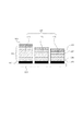
図1に示した有機EL発光装置を構成する有機EL素子(発光素子)は、基板100上に陽極として透明電極103が形成されている。透明電極103の内部には、周期構造300が形成されている。本実施の形態では透明電極103が光取り出し側の第2電極に対応する。さらに、この陽極の周縁を覆うように絶縁部材から成る素子分離層110が形成されている。素子分離層110の開口部から露出する陽極の露出部上に、発光層を含む有機層101が積層され、陰極である反射電極102が形成されている。本実施の形態では、反射電極102が第1電極に対応する。つまり、本実施の形態に係る有機EL発光装置は、基板100側から光を取り出すボトムエミッション型の発光装置の例である。
In the organic EL element (light emitting element) constituting the organic EL light emitting device shown in FIG. 1, a
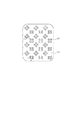
周期構造300は、本構成例では金属により構成され、図2に示すように、EL発光領域302の内側にフォトニック結晶構造(周期構造300)部分と平坦部分とをいずれも有している。なお、図1の透明電極103、有機層101、反射電極102が積層された部分に対応するのが、図2の発光領域(EL発光領域)302である。
The
有機層101は、図3に示すように、通常、ホール輸送層106、発光層105(R発光層115、G発光層125、B発光層135)、電子輸送層107が積層された構成をとる。発光層105は、それぞれの発光色に応じた蛍光性有機化合物若しくは燐光性有機化合物を含む。また、必要に応じて陽極とホール輸送層106との間にホール注入層108を、陰極と電子輸送層107との間に電子注入層109を設けてもよい。
As shown in FIG. 3, the
これらの有機EL素子に電圧を印加することで、陽極から注入された正孔と陰極から注入された電子が、有機層101中の発光層で再結合し、励起子を形成することで発光する。
By applying a voltage to these organic EL elements, holes injected from the anode and electrons injected from the cathode recombine in the light emitting layer in the
図1に示した構成例では、有機層101と反射電極102との界面が反射面となる。発光点201に対して、透明電極103側(第2電極側)が光取り出し側、反射電極側(第1電極側)が反射面側となる。ただし、本発明では反射面は有機層と電極との界面に形成される構成に限られない。反射面側の第1電極の構成は、光透過部材、金属層、或いはその積層であってもよい。第1電極が光透過部材である場合には、光透過性の誘電体を挟んで金属層が配置されている構成となり、反射面は金属層と誘電体との界面に形成される。光透過部材と金属層との積層の場合には、その界面が反射面となる。
In the configuration example shown in FIG. 1, the interface between the
反射面が存在すると、発光層から反射面へ入射する光と反射面で反射する光との重ね合わせによる干渉が生じる。発光層はこの干渉の腹(antinode)に形成される。発光層を干渉の腹に構成することで、発光層から光取り出し側に発光する光と、発光層から反射面側へ発光し反射面により反射される光とが干渉により強め合うことになる。つまり、干渉の腹とは、干渉による光の強め合いが極大になる位置のことである。 When the reflection surface exists, interference occurs due to the superposition of the light incident on the reflection surface from the light emitting layer and the light reflected by the reflection surface. The light emitting layer is formed on the antinode of this interference. By configuring the light emitting layer as an antinode of interference, the light emitted from the light emitting layer to the light extraction side and the light emitted from the light emitting layer to the reflective surface side and reflected by the reflective surface are strengthened by interference. In other words, the anti-interference is a position where the intensity of light due to the interference is maximized.
なお、発光層が干渉の腹に形成されるとは、発光層内の発光位置が干渉の腹の近傍に位置することである。発光位置が干渉の腹に位置することが好ましいが、発光層から発光する光のスペクトルピーク波長と外部に取り出そうとする光のスペクトルピーク波長とが異なる場合には、発光位置と干渉の腹とがずれていてもよい。具体的には、発光位置と干渉の腹との膜厚方向の差が、λ/8n以内にあればよい。発光強度は膜厚方向に分布を有するが、本発明における発光位置は膜厚方向で発光強度がピークとなる位置のことと定義する。発光位置を決める支配的な要因は、発光層へのキャリア注入バランス、即ち電子注入特性とホール注入特性のバランス及び発光層に用いられる材料のキャリア移動度であるが、キャリア注入バランスがほぼ均等である場合には、キャリア移動度が支配的な要因となる。 Note that the fact that the light emitting layer is formed on the antinode of interference means that the light emitting position in the light emitting layer is located in the vicinity of the antinode of interference. It is preferable that the light emission position is located at the antinode of interference, but when the spectrum peak wavelength of light emitted from the light emitting layer is different from the spectrum peak wavelength of light to be extracted outside, the light emission position and the antinode of interference are It may be shifted. Specifically, the difference in the film thickness direction between the light emitting position and the antinode of interference should be within λ / 8n. Although the emission intensity has a distribution in the film thickness direction, the emission position in the present invention is defined as the position where the emission intensity reaches a peak in the film thickness direction. The dominant factors that determine the light emitting position are the carrier injection balance to the light emitting layer, that is, the balance between electron injection characteristics and hole injection characteristics, and the carrier mobility of the material used for the light emitting layer. In some cases, carrier mobility is the dominant factor.
この場合、電子移動度がホール移動度よりも大きい場合には、発光層の陽極側の界面付近が発光位置となり、ホール移動度が電子移動度よりも大きい場合には、発光層の陰極側の界面付近が発光位置となる。 In this case, when the electron mobility is larger than the hole mobility, the vicinity of the anode side interface of the light emitting layer is a light emitting position, and when the hole mobility is larger than the electron mobility, the cathode side of the light emitting layer is located. The vicinity of the interface is the light emission position.
一方、本発明では、周期構造300は干渉の節(node)に構成される。周期構造が干渉の節に形成されるとは、周期構造の膜厚方向の中心が干渉の節の近傍に位置することである。干渉の節の近傍とは以下に詳細に説明するが、周期構造の膜厚方向の中心と干渉の節との差がλ/8n以内であることである。この範囲にある場合には、周期構造が発光層から光取り出し側に発光する光と、発光層から反射面側へ発光し反射面により反射される光との干渉に与える影響が少なくなるため、周期構造と干渉を両立させ飛躍的に光取り出し効率を高めることができる。
Meanwhile, in the present invention, the
一般に、有機EL素子では、発光層の屈折率(約1.7〜1.9程度)が、有機EL素子外部の空気の屈折率1.0よりも大きい。そのため、周期構造300がない場合、発光点201から発光される光の大部分は、全反射により基板水平方向(面内方向)への導波光203として、有機EL素子内部に閉じ込められてしまう。伝播光202として、有機EL素子外部に取り出して利用できる光の割合は、約20%程度でしかない。
In general, in an organic EL element, the refractive index of the light emitting layer (about 1.7 to 1.9) is larger than the refractive index 1.0 of air outside the organic EL element. Therefore, in the absence of the
これに対し、図1に示すように周期構造300が配置された場合は、導波光203の一部が周期構造300によって回折光204に変換され、有機EL素子外部に取り出される。この回折効果のため、発光効率が向上する。
On the other hand, when the
しかしながら、反射面を有する有機EL素子に周期構造を構成する場合、発光効率は周期構造と反射面間の光路長に依存して変化する。周期構造を反射面による干渉の節(node)に構成すると発光効率が向上する。一方、周期構造を反射面による干渉の腹(antinode)に構成すると発光効率は低下してしまう。 However, when a periodic structure is formed in an organic EL element having a reflective surface, the light emission efficiency varies depending on the optical path length between the periodic structure and the reflective surface. If the periodic structure is configured as a node of interference by the reflecting surface, the light emission efficiency is improved. On the other hand, if the periodic structure is configured as an antinode of interference by the reflecting surface, the light emission efficiency is lowered.
この現象を説明するために、反射面による干渉と周期構造の位置関係を示す概念図を図4に示す。図4aは、比較例として、平坦な反射面による干渉(干渉光)を模式的に示している。干渉の腹に発光層を配置することで、干渉強め合いにより発光が強められる。このような構成に、金属周期構造や低屈折率材料中に形成された高屈折率材料の周期構造のように、固定端の境界条件を生じる周期構造を配置することを考察する。図4b、図4cは本発明の構成例として、周期構造を干渉の節に設けた例を示している。図4bは反射面に周期構造を設けた例、図4cは反射面から離間する位置に周期構造を設けた例である。図4b、図4cのように、周期構造を干渉の節に構成すると、基板垂直方向の光の干渉強め合いを概ね保持したまま、基板水平方向の導波光を回折光に変換し、有機EL素子の外部に取り出すことが可能となる。したがって、光取り出し効率が向上する。これに対し、図4dのように、周期構造を干渉の腹に構成すると、干渉強め合いが損なわれて、発光効率が低下してしまう。 In order to explain this phenomenon, FIG. 4 is a conceptual diagram showing the positional relationship between the interference by the reflecting surface and the periodic structure. FIG. 4a schematically shows interference (interference light) by a flat reflecting surface as a comparative example. By arranging the light emitting layer on the antinode of interference, light emission is enhanced by interference strengthening. Consider the arrangement of a periodic structure that generates a boundary condition at the fixed end, such as a metal periodic structure or a periodic structure of a high refractive index material formed in a low refractive index material. 4b and 4c show an example in which a periodic structure is provided at an interference node as a configuration example of the present invention. 4B shows an example in which a periodic structure is provided on the reflecting surface, and FIG. 4C shows an example in which the periodic structure is provided at a position away from the reflecting surface. When the periodic structure is configured as an interference node as shown in FIGS. 4B and 4C, the guided light in the horizontal direction of the substrate is converted into the diffracted light while maintaining the interference enhancement of the light in the vertical direction of the substrate, and the organic EL element It becomes possible to take out to the outside. Therefore, the light extraction efficiency is improved. On the other hand, as shown in FIG. 4d, when the periodic structure is configured as an antinode of interference, the interference strengthening is lost and the light emission efficiency is lowered.
具体例として、周期構造と反射面間の光路長に対する発光強度比の関係を数値計算により評価した結果を図5にグラフとして示す。発光強度比は垂直方向の値で、周期構造がない場合を基準としている。電磁波の数値計算には、有機EL発光装置の断面を考え、FDTD法を用いた。波長範囲λ=380nm〜780nmで、5nm刻みで計算を行った。電磁波モードは、TE、TMモードで計算を行った。 As a specific example, the result of evaluating the relationship of the emission intensity ratio with respect to the optical path length between the periodic structure and the reflecting surface by numerical calculation is shown as a graph in FIG. The emission intensity ratio is a value in the vertical direction and is based on the case where there is no periodic structure. For the numerical calculation of electromagnetic waves, the FDTD method was used considering the cross section of the organic EL light emitting device. The calculation was performed in 5 nm increments in the wavelength range λ = 380 nm to 780 nm. The electromagnetic wave mode was calculated in the TE and TM modes.
図5で周期構造が干渉の節(node)に位置する場合の光路長の範囲を網掛けで示す。それ以外は、干渉の腹(antinode)となる光路長の範囲である。図5より、周期構造を干渉の節に構成すると、周期構造がない有機EL素子と比較し、発光強度が向上する。一方、周期構造を干渉の腹に構成すると、周期構造がない有機EL素子と比較し、発光強度が低下してしまう。 In FIG. 5, the range of the optical path length when the periodic structure is located at the node of interference is shown by shading. Other than that, it is the range of the optical path length which becomes the antinode of interference. As shown in FIG. 5, when the periodic structure is configured as an interference node, the emission intensity is improved as compared with an organic EL element having no periodic structure. On the other hand, when the periodic structure is configured as an antinode of interference, the emission intensity is reduced as compared with an organic EL element having no periodic structure.
したがって、本発明では、発光効率を向上させるために、反射面による干渉の節に周期構造を構成する。よって、発光素子の発光効率を向上することが可能となる。 Therefore, in the present invention, in order to improve the light emission efficiency, a periodic structure is formed at the node of interference by the reflecting surface. Thus, the light emission efficiency of the light emitting element can be improved.
また、高屈折率材料中に形成された低屈折率材料の周期構造のように、自由端の境界条件を生じる周期構造を配置する場合は、周期構造を干渉の腹に構成することが望ましい。 In addition, when a periodic structure that generates a boundary condition at the free end, such as a periodic structure of a low-refractive index material formed in a high-refractive index material, is disposed, it is desirable to configure the periodic structure at the antinode of interference.
以下、より詳細な説明を行う。 A more detailed description will be given below.
周期構造が反射面による干渉の節に位置するための条件は、外部に取り出される光のスペクトルのピーク波長をλ、周期構造と反射面間の距離をd、周期構造と反射面間の平均屈折率をnとして数1で与えられる。ここで、反射面の位相シフトφm、整数mである。また、距離dと平均屈折率nは、周期構造と反射面間の各層iの厚さをdi、屈折率をniとして、それぞれ、d=Σdi、n=Σnidi/dで表される。 The condition for the periodic structure to be positioned at the node of interference by the reflecting surface is that the peak wavelength of the spectrum of the light extracted outside is λ, the distance between the periodic structure and the reflecting surface is d, and the average refraction between the periodic structure and the reflecting surface. The rate is given by the following equation (1). Here, the phase shift φ m of the reflecting surface is an integer m. The distance d and the average refractive index n, the thickness of each layer i between the periodic structure and the reflective surface d i, a refractive index as n i, respectively, d = [Sigma] d i, with n = .SIGMA.n i d i / d expressed.

反射面が金属から構成される場合は、φm〜−πである。図4bのように、周期構造が、反射面に接した干渉の節に構成される場合、m=−1に対応する。図6に、発光層の基板反対側が光取り出し側となるトップエミッション構成を示す。図6の構成例では、金属からなる反射電極102と反射電極上の透明電極103の界面が反射面となり、反射面に周期構造300が構成されており、m=−1の場合である。また、図4cのように、周期構造が反射面から離間した干渉の節に位置する場合は、m≧0に対応する。図1の本構成例は、m≧0の場合である。
When the reflecting surface is made of metal, it is φ m to −π. As shown in FIG. 4b, when the periodic structure is configured at an interference node in contact with the reflecting surface, m = -1. FIG. 6 shows a top emission configuration in which the opposite side of the light emitting layer to the substrate is the light extraction side. In the configuration example of FIG. 6, the interface between the
さらに、周期構造の高さ方向の凹凸に従って場所ごとに光路長が変化し、反射面による干渉に影響を及ぼす。よって、干渉強め合いをより良く保持するには、周期構造の凹凸いずれの領域においても、数1を満たす必要があり、周期構造の基板面に対して垂直方向の高さをhとして、数2の条件式で与えられる。したがって、周期構造の高さhを上限値λ/(4n)より低く抑えることが望ましい。 Furthermore, the optical path length changes from place to place in accordance with the unevenness in the height direction of the periodic structure, which affects interference by the reflecting surface. Therefore, in order to better maintain interference strengthening, it is necessary to satisfy Equation 1 in any region of the irregularity of the periodic structure, and the height in the direction perpendicular to the substrate surface of the periodic structure is h, and Equation 2 Is given by the conditional expression. Therefore, it is desirable to keep the height h of the periodic structure lower than the upper limit value λ / (4n).
有機EL素子では、平均屈折率は、n=1.5〜2.0程度、可視域での発光波長λは380nm〜780nmであるから、周期構造の高さは、130nmより小さいであることが望ましい。また、赤色発光素子、緑色発光素子、青色発光素子(以下R素子、G素子、B素子とする。)で周期構造の高さが共通の場合は、波長の最も短いB(青)で数3の条件を満たす必要があるため、60nmより小さいことが望ましい。R素子、G素子、B素子で周期構造の高さを共通にする場合、周期構造の形成をまとめて行うことができる。さらに、発光層の段切れを防いで電流リークや発光不均一化を防ぐためには発光層の平坦化が求められ、発光層の平坦化のためには、周期構造の高さが30nmより小さことがより望ましい。特に、有機EL素子においては、有機層(発光層)の段切れによる電流リークや発光不均一化の問題が顕著であるため、周期構造の高さを低くすることが好ましい。 In the organic EL element, the average refractive index is about n = 1.5 to 2.0, and the emission wavelength λ in the visible range is 380 nm to 780 nm. Therefore, the height of the periodic structure may be smaller than 130 nm. desirable. Further, when the red light emitting element, the green light emitting element, and the blue light emitting element (hereinafter referred to as “R element”, “G element”, and “B element”) have a common height of the periodic structure, B (blue) having the shortest wavelength is represented by several 3 Since it is necessary to satisfy the above condition, it is desirable that the thickness is smaller than 60 nm. When the height of the periodic structure is shared by the R element, the G element, and the B element, the periodic structure can be formed collectively. Furthermore, in order to prevent the light emitting layer from being disconnected and to prevent current leakage and light emission non-uniformity, the light emitting layer needs to be flattened. For the flattening of the light emitting layer, the height of the periodic structure is smaller than 30 nm. Is more desirable. In particular, in an organic EL element, problems such as current leakage and non-uniform light emission due to disconnection of the organic layer (light emitting layer) are significant, and therefore it is preferable to reduce the height of the periodic structure.
とはいえ周期構造は、発光層よりも基板側に形成する、つまり発光層と基板との間に形成することが好ましい。発光層の光取り出し側に形成する場合、周期構造による発光層の段切れの問題は解決されるが、発光層(有機層)に影響を与えることなく周期構造を形成することが困難であるためである。 However, the periodic structure is preferably formed on the substrate side of the light emitting layer, that is, between the light emitting layer and the substrate. When forming on the light extraction side of the light emitting layer, the problem of step breakage of the light emitting layer due to the periodic structure is solved, but it is difficult to form the periodic structure without affecting the light emitting layer (organic layer). It is.
図2に示すように、本構成例では、周期構造300が存在する部分と存在しない部分から構成される。ここで、周期構造300の周期を規定する2つの基本格子ベクトルをa1、a2とする。また、これらの基本格子ベクトルa1、a2に対し、数3の関係を満たす基本逆格子ベクトルをb1、b2とする。図2の例では、周期構造300が存在する部分と存在しない部分が、より大きな周期で配列された階層構造となっている。ここで、より大きな周期を規定する2つの基本格子ベクトルはA1、A2である。図2の例では、発光素子の上下左右で同じ視野角特性となるように、周期構造300が4回対称性を有する構造となっている。本発明の発光素子を表示装置として用いる場合には、表示装置の上下左右の視野角特性を同じにするために、周期構造の基本格子ベクトル方向と表示領域の上下方向、左右方向を合わせることが好ましい。
As shown in FIG. 2, this configuration example includes a portion where the
![]()
![]()
周期構造による回折の効果を高めるためには、周期構造の周期を設定することがより好ましい。以下周期構造の周期について説明する。 In order to enhance the effect of diffraction by the periodic structure, it is more preferable to set the period of the periodic structure. Hereinafter, the period of the periodic structure will be described.
有機層101中の発光層からの発光ピーク波長をλとし、波数をk=2π/λとする。また、発光層の屈折率をn、光取り出し側媒体(通常は空気)の屈折率をnextとし、条件n>nextを満たすとする。
The emission peak wavelength from the light emitting layer in the
光導波路301を伝播する導波光203に対する基板100の水平方向への伝播係数をβとし、導波光203に対する有効屈折率neff及び有効吸収係数κeffを、数4により定義する。有効屈折率neffは、条件next<neff<nを満たす。
The propagation coefficient in the horizontal direction of the
![]()
![]()
このとき、回折条件は水平方向の位相整合条件から、2つの整数m1、m2を回折次数とし、基板法線方向に対する回折角度をθとして、条件next<neff<nのもとで、数5で与えられる。 At this time, the diffraction condition is based on the condition of n ext <n eff <n, where two integers m 1 and m 2 are diffraction orders and the diffraction angle with respect to the substrate normal direction is θ, based on the phase matching condition in the horizontal direction. , Given by Equation 5.
正方格子の場合は、周期をaとして、基本格子ベクトルは数6となり、基本逆格子ベクトルは数7となる。 In the case of a square lattice, the period is a, the basic lattice vector is Equation 6, and the basic reciprocal lattice vector is Equation 7.
この時、数5の回折条件は、数8となる。 At this time, the diffraction condition of Formula 5 is expressed by Formula 8.
ここで、どちらか一方の1次元方向に着目し、m2=0(もしくは、m1=0)および、|m1|=m>0(もしくは、|m2|=m>0)とする。この時、数8の回折条件は、簡略化され数9となる。さらに、有機EL素子のように、3next>n≧neffの関係を満たす場合、m=1の1次の回折光のみが生じるための回折条件は、数10となる。 Here, paying attention to one of the one-dimensional directions, m 2 = 0 (or m 1 = 0) and | m 1 | = m> 0 (or | m 2 | = m> 0). . At this time, the diffraction condition of Equation 8 is simplified and becomes Equation 9. Further, when the relationship of 3n ext > n ≧ n eff is satisfied as in the case of an organic EL element, the diffraction condition for generating only the first-order diffracted light with m = 1 is expressed by Equation 10.
有機EL素子の発光パターンや効率、色度などの制御を可能とするには、1次の回折光のみを発生させ、また、導波光のモード数を少なくすることが望ましい。有機EL素子では、通常、発光層の屈折率はn=1.6〜2.0程度、光取り出し側の屈折率はnext=1.0である。よって、数10から、主に1次の回折光のみを利用する場合は、周期構造300の周期aは、概ね発光ピーク波長λの0.33倍以上1.0倍以下が望ましい。可視光の波長域が380nm以上780nm以下であることから、周期構造300の周期aは、125nm以上780nm以下であることが望ましい。R素子、G素子、B素子のそれぞれで周期構造の周期が数10を満たすためには、R素子の周期を最も長く、B素子の周期を最も短くすることが好ましい。
In order to enable control of the light emission pattern, efficiency, chromaticity, and the like of the organic EL element, it is desirable to generate only the first-order diffracted light and reduce the number of modes of guided light. In the organic EL element, the refractive index of the light emitting layer is usually about n = 1.6 to 2.0, and the refractive index on the light extraction side is n ext = 1.0. Therefore, when using only the first-order diffracted light from Equation 10, it is desirable that the period a of the
なお、これまでは、基板側を陽極、光取り出し側を陰極とする構成で説明してきたが、基板側を陰極、光取り出し側を陽極とし、ホール輸送層、発光層、電子輸送層を逆順に積層した構成においても本発明を実施することは可能である。したがって、本発明にかかる発光装置は基板側を陽極、光取り出し側を陰極とする構成に限定されるものではない。 In the above description, the substrate side is the anode and the light extraction side is the cathode. However, the substrate side is the cathode, the light extraction side is the anode, and the hole transport layer, light emitting layer, and electron transport layer are in reverse order. The present invention can be implemented even in a stacked configuration. Therefore, the light emitting device according to the present invention is not limited to the configuration in which the substrate side is an anode and the light extraction side is a cathode.
また、図3のホール輸送層106、発光層105、電子輸送層107、ホール注入層108、電子注入層109に用いられる有機化合物としては、低分子材料、高分子材料、若しくはその両方により構成され、特に限定されるものではない。さらに、必要に応じて無機化合物やQD(量子ドット)を用いてもよい。
Further, the organic compound used for the
さらに、周期構造300は、上述したように2次元的なフォトニック結晶構造に限定されず、1次元的な回折格子の組み合わせや3次元的なフォトニック結晶構造でもよい。また、図6では凸型のフォトニック結晶構造を示したが、図7のように凹型のフォトニック結晶構造でもよい。
Furthermore, the
さらに、図8のように、異なる基本格子ベクトルを持つ複数種類の周期構造300をいずれも有する構成であってもよい。図8の例は、基本格子ベクトルa1、a2の周期構造と基本格子ベクトルa’1、a’2の周期構造を組み合わせた場合である。a’1は(a1+a2)/√2方向のベクトルであり、a’2は(−a1+a2)/√2方向のベクトルである。つまり、周期構造は、4回対称性を有する周期構造1と、周期構造1を45°回転した周期構造2を組み合わせた構造になっている。図8のように周期構造を配置することにより、発光素子の上下方向と左右方向の視野角特性だけでなく、発光素子の斜め方向の視野角特性も同じにすることができる。また、同様に、周期構造は、Nを自然数として、N回対称性を有する周期構造1と、周期構造1を180°/N回転した周期構造2を組み合わせた構造とすることができる。
Further, as shown in FIG. 8, the structure may include any of a plurality of types of
周期構造300は、完全に周期的である必要はなく、準結晶構造やフラクタル構造、連続的に周期構造が変化する構造、周期構造中に不規則な欠陥が存在する構造、若しくは周期構造とこれらを組み合わせたものでもよい。
The
さらに、以上の説明では、基板側が光取り出し側となるボトムエミッション構成について説明してきたが、基板の反対側が光取り出し側となるトップエミッション構成においても本発明は実施可能である。図6及び図7では、発光層より基板側に位置する反射面に周期構造を形成する例としている。すなわち、基板100上に周期構造300を有する反射電極102と反射電極上の透明電極103Bを形成し、その上に有機層101、透明電極104を積層したトップエミッション構成を示している。
Further, in the above description, the bottom emission configuration in which the substrate side is the light extraction side has been described, but the present invention can also be implemented in a top emission configuration in which the opposite side of the substrate is the light extraction side. 6 and 7 show an example in which a periodic structure is formed on the reflective surface located on the substrate side of the light emitting layer. That is, a top emission configuration is shown in which the
さらに、図6において、金属からなる反射電極102と可視光の波長領域では誘電体とみなせる反射電極上の透明電極103Bとの界面(金属反射面)を基板水平方向に伝播し、導波光の一種と考えられる表面プラズモンが生じる。よって、反射電極102と反射電極上の透明電極103Bとの界面を光導波路として利用可能である。表面プラズモンの伝播係数βspを、数4の伝播係数βとすると、通常の導波光と同様に回折条件は数5で与えられる。表面プラズモンを生じる界面としては、金属と透明電極界面に限られず、金属と有機層界面や金属と誘電体層界面でも可能である。
Further, in FIG. 6, the interface (metal reflection surface) between the
本発明の発光装置は、表示装置や、照明、表示装置用のバックライト等の様々な用途に適用することができる。表示装置としては、テレビ受像機、パーソナルコンピュータのディスプレイ、撮像装置の背面表示部、携帯電話の表示部、携帯音楽再生装置の表示部、携帯情報端末(PDA)の表示部、携帯ゲーム機の表示部、カーナビゲーションシステムの表示部等がある。 The light emitting device of the present invention can be applied to various uses such as a display device, illumination, and a backlight for the display device. As a display device, a television receiver, a display of a personal computer, a rear display unit of an imaging device, a display unit of a mobile phone, a display unit of a portable music player, a display unit of a personal digital assistant (PDA), a display of a portable game machine And a display unit of a car navigation system.
以下、本発明の発光素子の製造方法を実施例として説明するが、本発明は本実施例によって何ら限定されるものではない。 Hereinafter, although the manufacturing method of the light emitting element of this invention is demonstrated as an Example, this invention is not limited at all by this Example.
<参考例1>
図1に示す構成の有機EL素子を以下に示す方法で作製する。つまり、本参考例1の発光素子は、第1電極と光取り出し側の第2電極との間に発光層を有し、前記発光層よりも前記第1電極側に反射面が構成されている。
< Reference Example 1>
The organic EL element having the configuration shown in FIG. 1 is produced by the following method. That is, the light-emitting element of Reference Example 1 has a light-emitting layer between the first electrode and the second electrode on the light extraction side, and a reflective surface is formed on the first electrode side with respect to the light-emitting layer. .
まず、基板100上に、透明電極103として、スパッタリングによりITOを70nmの膜厚で形成する。
First, ITO is formed with a film thickness of 70 nm on the
次に、リフトオフ加工により、Alからなる周期構造300を形成する。まず、透明電極103上に、ポジ型のレジストをスピンコートしプリベークを行う。その後、レジストに図2に示すような正方格子の周期構造パターンを露光し、現像、ポストベークを行いレジストパターンを形成する。本参考例1では、周期構造300は周期240nm、一辺の長さ100nmとされる。また、10周期ごとに周期構造300が存在する部分と平坦な部分とが交互に並んでいる。次に、蒸着によりAlを30nmの膜厚で形成する。露光部分ではITO上にAlが形成され、露光部分以外ではレジスト上にAlが形成される。その後、レジストを剥離し、レジスト上のAlごと取り除くことにより、Alからなる周期構造300を形成する。この上に、スパッタリングによりITOを150nmの膜厚で形成して電極のパターニングをし、フォトニック結晶付きの陽極を形成する。
Next, the
図2のような正方格子では、発光素子の上下方向と左右方向とで周期構造300の周期(配列)が等しい。そのため、発光素子を視認した場合、上下方向と左右方向とで同様の光学特性を得ることができ、視認性を高めることができる。また、逆に、上下方向と左右方向の周期が異なる四角格子としてもよい。この場合は、方向によって視認性を調整することが可能となる。さらに、図8のように、異なる正方格子を組み合わせることにより、上下方向、左右方向と斜め方向とで同様の光学特性を得ることができ、視認性を高めることができる。
In the square lattice as shown in FIG. 2, the period (array) of the
さらに、酸化窒化珪素(SiNxOy)の素子分離層110を320nmの膜厚で形成した後、各副画素にEL発光領域となる開口部をエッチングし、フォトニック結晶を配置した陽極基板を作製する。
Further, after forming an
これをイソプロピルアルコール(IPA)で超音波洗浄し、次いで、煮沸洗浄後乾燥する。その後、UV/オゾン洗浄してから有機層101を真空蒸着により形成する。
This is subjected to ultrasonic cleaning with isopropyl alcohol (IPA) and then dried after boiling and drying. Thereafter, the
まず、下記構造式で示される化合物[I]を、ホール輸送層として70nmの膜厚で形成する。この際の真空度は1×10⁻⁴Pa、蒸着レートは、0.2nm/secである。 First, Compound [I] represented by the following structural formula is formed with a film thickness of 70 nm as a hole transport layer. The degree of vacuum at this time is 1 × 10 −4 Pa, and the deposition rate is 0.2 nm / sec.
次に、発光層を形成する。ホストとしてtris‐(8‐hydroxyquinoline)Aluminum(以下、Alq3と呼ぶ)と、発光性化合物3‐(2’‐Benzothiazolyl)‐7‐N,N‐diethylaminocoumarin(以下、クマリン6と呼ぶ)とを共蒸着して25nmの膜厚で発光層を形成する。蒸着時の真空度は1×10⁻⁴Pa、成膜速度は0.2nm/secである。 Next, a light emitting layer is formed. Co-evaporated tris- (8-hydroxyquinoline) Aluminum (hereinafter referred to as Alq3) and a luminescent compound 3- (2′-Benzothiazolyl) -7-N, N-diethylaminocoumarin (hereinafter referred to as Coumarin 6) as hosts Then, a light emitting layer is formed with a film thickness of 25 nm. The degree of vacuum during vapor deposition is 1 × 10 −4 Pa, and the film formation rate is 0.2 nm / sec.
さらに、電子輸送層として、1、10‐Bathophenanthroline(以下、BPhenと呼ぶ)を真空蒸着法にて10nmの膜厚で形成する。蒸着時の真空度は1×10⁻⁴Pa、成膜速度は0.2nm/secである。次に、電子注入層として、BPhenとCs2CO3とを共蒸着(重量比90:10)し、25nmの膜厚で形成する。蒸着時の真空度は3×10−4Pa、成膜速度は0.2nm/secである。 Further, 1, 10-Bathophanethroline (hereinafter referred to as BPhen) is formed to a thickness of 10 nm by vacuum deposition as an electron transport layer. The degree of vacuum during vapor deposition is 1 × 10 −4 Pa, and the film formation rate is 0.2 nm / sec. Next, as an electron injection layer, BPhen and Cs 2 CO 3 are co-evaporated (weight ratio 90:10) and formed to a thickness of 25 nm. The degree of vacuum at the time of vapor deposition is 3 × 10 −4 Pa, and the film formation rate is 0.2 nm / sec.
電子注入層まで形成した基板を、真空を破ること無しにスパッタ装置に移動し、反射電極102として、スパッタリングによりAg合金を200nmの膜厚で形成する。Ag合金からなる反射電極102は、可視光の波長域(λ=380nm〜780nm)で分光反射率80%以上の高反射電極である。Ag合金以外に、AlやAl合金などを用いてもよい。
The substrate on which the electron injection layer has been formed is moved to a sputtering apparatus without breaking the vacuum, and an Ag alloy is formed to a thickness of 200 nm by sputtering as the
さらに、発光装置の周辺部に吸湿剤を配置し、エッチングされたキャップガラスで封止することにより、有機EL発光装置を得る。つまり、反射面による干渉の節に金属の周期構造が配置される構成とされている。 Furthermore, an organic EL light emitting device is obtained by disposing a hygroscopic agent in the periphery of the light emitting device and sealing with an etched cap glass. That is, the metal periodic structure is arranged at the node of interference by the reflecting surface.
<比較例1>
まず、基板100上に、透明電極103として、スパッタリングによりITOを190nmの膜厚で形成して電極のパターニングをし、陽極を形成する。素子分離層110の形成以降は参考例1と同様である。つまり、周期構造を有さない構成とされている。
<Comparative Example 1>
First, as a
<比較例2>
まず、基板100上に、透明電極103として、スパッタリングによりITOを140nmの膜厚で形成する。次に、Alからなる周期構造300の形成までは、参考例1と同様である。この上に、スパッタリングによりITOを35nmの膜厚で形成して電極のパターニングをし、フォトニック結晶付きの陽極を形成する。素子分離層110の形成以降は参考例1と同様である。つまり、反射面による干渉の腹領域に金属の周期構造が配置される構成とされている。
<Comparative example 2>
First, ITO is formed as a
表1に、参考例1と比較例1、比較例2における発光強度比(垂直方向)の数値計算による評価値を示す。発光強度比が約1.2倍となり、光取り出し効率が向上することがわかった。 Table 1 shows evaluation values by numerical calculation of the emission intensity ratio (in the vertical direction) in Reference Example 1, Comparative Example 1, and Comparative Example 2. It was found that the light emission intensity ratio was about 1.2 times and the light extraction efficiency was improved.
参考例1の光取り出し効率が向上したのは、発光層から透明電極の方向に進む光と発光層から反射電極の方向に進み反射面で反射する光とによって生じる干渉が周期構造から受ける影響が少ないためである。そのため、干渉による光取り出し効率の向上と周期構造による光取り出し効率の向上を両立することができ、比較例1に比べて光取り出し効率が向上した。比較例2は発光層から透明電極の方向に進む光と発光層から反射電極の方向に進み反射面で反射する光とによって生じる干渉が周期構造から影響を受けたため、比較例1に比べて光取り出し効率が低くなった。なお、表1の実施例1とは参考例1のことである。 The light extraction efficiency of the reference example 1 is improved because interference caused by light traveling from the light emitting layer toward the transparent electrode and light traveling from the light emitting layer toward the reflective electrode and reflected by the reflecting surface is affected by the periodic structure. This is because there are few. Therefore, the improvement of the light extraction efficiency due to interference and the improvement of the light extraction efficiency due to the periodic structure can both be achieved, and the light extraction efficiency is improved as compared with Comparative Example 1. In Comparative Example 2, the interference caused by the light traveling from the light emitting layer in the direction of the transparent electrode and the light traveling from the light emitting layer in the direction of the reflective electrode and reflected from the reflective surface is affected by the periodic structure. The extraction efficiency was low. In addition, Example 1 in Table 1 is Reference Example 1.
<実施例1>
図7に示す構成の有機EL素子を以下に示す方法で作製する。
<Example 1 >
The organic EL element having the configuration shown in FIG. 7 is manufactured by the following method.
まず、基板100上に、反射電極102として、スパッタリングによりAg合金を約150nmの膜厚で形成する。
First, an Ag alloy is formed as a
この反射電極102上に、まず、ポジ型のレジストをスピンコートしプリベークを行う。その後、レジストに図2に示すような正方格子の周期構造パターンを露光し、現像、ポストベークを行いレジストパターンを形成する。
First, a positive resist is spin-coated on the
エッチング加工により、反射電極102表面に周期構造300を形成する。本実施例1では、周期構造300は周期250nm、一辺の長さ140nm、エッチング深さ40nmとされる。また、10周期ごとに周期構造300が存在する部分と平坦な部分とが交互に並んでいる。
The
次に、IZOのリフトオフ加工により、周期構造300の凹状にへこんだエッチング部分を平坦化する。レジストパターンを残した状態で、スパッタリングにより透明導電性材料のIZOを40nmの膜厚で形成する。エッチング部分ではAg合金上にIZOを、エッチング部分以外ではレジスト上にIZOを形成する。その後、レジストを剥離し、レジスト上のIZOごと取り除いて平坦化する。この上に、スパッタリングによりIZOを20nmの膜厚で形成して電極のパターニングをし、フォトニック結晶付きの陽極を形成する。
Next, the etched portion of the
さらに、酸化窒化珪素(SiNxOy)の素子分離層110を320nmの膜厚で形成した後、各副画素にEL発光領域となる開口部をエッチングし、フォトニック結晶を配置した陽極基板を作製する。
Further, after forming an
これをイソプロピルアルコール(IPA)で超音波洗浄し、次いで、煮沸洗浄後乾燥する。その後、UV/オゾン洗浄してから有機層101を真空蒸着により形成する。
This is subjected to ultrasonic cleaning with isopropyl alcohol (IPA) and then dried after boiling and drying. Thereafter, the
まず、化合物[I]を、ホール輸送層として155nmの膜厚で形成する。この際の真空度は1×10⁻⁴Pa、蒸着レートは、0.2nm/secである。 First, compound [I] is formed with a film thickness of 155 nm as a hole transport layer. The degree of vacuum at this time is 1 × 10 −4 Pa, and the deposition rate is 0.2 nm / sec.
次に、発光層を形成する。発光層としては、ホストとしてAlq3と、発光性化合物クマリン6とを共蒸着して30nmの膜厚で発光層を形成する。蒸着時の真空度は1×10⁻⁴Pa、成膜速度は0.2nm/secである。 Next, a light emitting layer is formed. As the light emitting layer, Alq3 as a host and the light emitting compound coumarin 6 are co-evaporated to form a light emitting layer with a thickness of 30 nm. The degree of vacuum during vapor deposition is 1 × 10 −4 Pa, and the film formation rate is 0.2 nm / sec.
さらに、電子輸送層として、BPhenを真空蒸着法にて10nmの膜厚で形成する。蒸着時の真空度は1×10⁻⁴Pa、成膜速度は0.2nm/secである。次に、電子注入層として、BPhenとCs2CO3とを共蒸着(重量比90:10)し、30nmの膜厚で形成する。蒸着時の真空度は3×10−4Pa、成膜速度は0.2nm/secである。 Further, BPhen is formed with a film thickness of 10 nm by vacuum deposition as an electron transport layer. The degree of vacuum during vapor deposition is 1 × 10 −4 Pa, and the film formation rate is 0.2 nm / sec. Next, as an electron injection layer, BPhen and Cs 2 CO 3 are co-evaporated (weight ratio 90:10) and formed to a thickness of 30 nm. The degree of vacuum at the time of vapor deposition is 3 × 10 −4 Pa, and the film formation rate is 0.2 nm / sec.
電子注入層まで形成した基板を、真空を破ること無しにスパッタ装置に移動し、金属半透明電極104として、スパッタリングによりAg合金を24nmの膜厚で形成する。
The substrate formed up to the electron injection layer is moved to a sputtering apparatus without breaking the vacuum, and an Ag alloy is formed to a thickness of 24 nm by sputtering as the metal
さらに、誘電体層104Bとして、スパッタリングによりシリカを290nmの膜厚で形成する。 Further, as the dielectric layer 104B, silica is formed with a thickness of 290 nm by sputtering.
さらに、発光装置の周辺部に吸湿剤を配置し、エッチングされたキャップガラスで封止することにより、有機EL発光装置を得る。 Furthermore, an organic EL light emitting device is obtained by disposing a hygroscopic agent in the periphery of the light emitting device and sealing with an etched cap glass.
<比較例3>
反射電極102の形成までは、実施例1と同様である。スパッタリングによりIZOを20nmの膜厚で形成して電極のパターニングをし、陽極を形成する。ホール輸送層の形成以降は、実施例1と同様である。つまり、周期構造を有さない構成とされている。
<Comparative Example 3>
The processes until the formation of the
表2に、実施例1と比較例3における発光強度比(垂直方向)の数値計算による評価値を示す。発光強度比が約1.8倍となり、発光効率が向上することがわかった。 Table 2 shows evaluation values by numerical calculation of the emission intensity ratio (in the vertical direction) in Example 1 and Comparative Example 3. It was found that the emission intensity ratio was about 1.8 times and the emission efficiency was improved.
実施例1の光取り出し効率が向上したのは、発光層から透明電極の方向に進む光と発光層から反射電極の方向に進み反射面で反射する光とによって生じる干渉が周期構造から受ける影響が少ないためである。そのため、干渉による光取り出し効率の向上と周期構造による光取り出し効率の向上を両立することができ、比較例3に比べて光取り出し効率が向上した。 The light extraction efficiency of Example 1 was improved because interference caused by light traveling from the light emitting layer in the direction of the transparent electrode and light traveling from the light emitting layer to the reflective electrode and reflected from the reflective surface is affected by the periodic structure. This is because there are few. Therefore, the improvement of the light extraction efficiency due to interference and the improvement of the light extraction efficiency due to the periodic structure can both be achieved, and the light extraction efficiency is improved as compared with Comparative Example 3.
100 基板
101 有機層
102 反射電極
103 透明電極
103B 反射電極上の透明電極
104 金属半透明電極
104B 誘電体層
105 発光層
106 ホール輸送層
107 電子輸送層
108 ホール注入層
109 電子注入層
110 素子分離層
201 発光点
202 伝播光
203 導波光
204 回折光
300 周期構造
301 光導波路
302 EL発光領域
DESCRIPTION OF
Claims (8)
前記発光層よりも前記第1電極側に反射面があり、前記発光層から前記第2電極側に発光する光と、前記発光層から前記反射面側へ発光し前記反射面により反射される光とを干渉により強め合わせる発光素子において、
前記発光層で発生し前記発光素子の面内方向に導波する光を前記発光素子の外に出射させる周期構造を有し、
前記周期構造が、固定端の境界条件を生じる周期構造であり、かつ、前記干渉の節である前記反射面に配置され、
前記発光層が前記干渉の腹に配置されていることを特徴とする発光素子。 A first electrode, a second electrode on the light emission side, and a light emitting layer between the first electrode and the second electrode,
There is a reflective surface on the first electrode side of the light emitting layer, light emitted from the light emitting layer to the second electrode side, and light emitted from the light emitting layer to the reflective surface side and reflected by the reflective surface In a light-emitting element that strengthens and by interference,
Having a periodic structure for emitting light generated in the light emitting layer and guided in the in-plane direction of the light emitting element to the outside of the light emitting element;
The periodic structure is a periodic structure that generates a boundary condition of a fixed end, and is disposed on the reflecting surface that is a node of the interference ,
The light emitting element, wherein the light emitting layer is arranged on the antinode of the interference .
を満たすことを特徴とする請求項1に記載の発光素子。 The height h of the periodic structure is the peak wavelength λ of the spectrum of light emitted to the outside, and the average refractive index n between the periodic structure and the reflecting surface,
The light-emitting element according to claim 1, wherein:
前記赤色を発する発光素子と前記緑色を発する発光素子と前記青色を発する発光素子が請求項1乃至請求項5のいずれか1項に記載の発光素子であることを特徴とする発光装置。 A light-emitting device having a light-emitting element that emits red light, a light-emitting element that emits green light, and a light-emitting element that emits blue light,
The light emitting device characterized in that the light-emitting element which emits the blue light-emitting element which emits the green light-emitting element which emits the red is a light-emitting device according to any one of claims 1 to 5.
Priority Applications (3)
| Application Number | Priority Date | Filing Date | Title |
|---|---|---|---|
| JP2007328709A JP5219493B2 (en) | 2007-11-14 | 2007-12-20 | Light emitting element and light emitting device using the same |
| US12/674,240 US8232572B2 (en) | 2007-11-14 | 2008-11-13 | Light emitting device |
| PCT/JP2008/071060 WO2009064020A1 (en) | 2007-11-14 | 2008-11-13 | Light emitting device |
Applications Claiming Priority (5)
| Application Number | Priority Date | Filing Date | Title |
|---|---|---|---|
| JP2007295591 | 2007-11-14 | ||
| JP2007295974 | 2007-11-14 | ||
| JP2007295974 | 2007-11-14 | ||
| JP2007295591 | 2007-11-14 | ||
| JP2007328709A JP5219493B2 (en) | 2007-11-14 | 2007-12-20 | Light emitting element and light emitting device using the same |
Publications (3)
| Publication Number | Publication Date |
|---|---|
| JP2009140894A JP2009140894A (en) | 2009-06-25 |
| JP2009140894A5 JP2009140894A5 (en) | 2012-11-01 |
| JP5219493B2 true JP5219493B2 (en) | 2013-06-26 |
Family
ID=40871294
Family Applications (1)
| Application Number | Title | Priority Date | Filing Date |
|---|---|---|---|
| JP2007328709A Expired - Fee Related JP5219493B2 (en) | 2007-11-14 | 2007-12-20 | Light emitting element and light emitting device using the same |
Country Status (2)
| Country | Link |
|---|---|
| US (1) | US8232572B2 (en) |
| JP (1) | JP5219493B2 (en) |
Families Citing this family (29)
| Publication number | Priority date | Publication date | Assignee | Title |
|---|---|---|---|---|
| JP2011203701A (en) * | 2010-03-04 | 2011-10-13 | Asahi Kasei E-Materials Corp | Diffraction grating substrate |
| JP5553890B2 (en) * | 2010-03-15 | 2014-07-16 | パイオニア株式会社 | Organic EL device and manufacturing method thereof, organic photoelectric conversion device |
| WO2011114424A1 (en) * | 2010-03-15 | 2011-09-22 | パイオニア株式会社 | Organic el panel and method for producing same |
| JP5676949B2 (en) * | 2010-07-21 | 2015-02-25 | キヤノン株式会社 | Organic EL display device |
| JP5744594B2 (en) | 2011-03-30 | 2015-07-08 | パナソニック株式会社 | Organic EL device and method for manufacturing the same |
| US20140203273A1 (en) * | 2011-09-21 | 2014-07-24 | Panasonic Corporation | Organic electroluminescence element |
| KR102001815B1 (en) * | 2011-11-29 | 2019-07-19 | 가부시키가이샤 한도오따이 에네루기 켄큐쇼 | Method of manufacturing sealed body and method of manufacturing light-emitting device |
| JP6118525B2 (en) | 2012-09-03 | 2017-04-19 | 出光興産株式会社 | Organic electroluminescence device and electronic device |
| WO2014084159A1 (en) * | 2012-11-27 | 2014-06-05 | 昭和電工株式会社 | Organic el element and method for manufacturing same |
| CN105940508B (en) | 2014-02-28 | 2019-01-11 | 松下知识产权经营株式会社 | Luminescent device and light emitting device |
| US9518215B2 (en) | 2014-02-28 | 2016-12-13 | Panasonic Intellectual Property Management Co., Ltd. | Light-emitting device and light-emitting apparatus |
| WO2015129224A1 (en) | 2014-02-28 | 2015-09-03 | パナソニックIpマネジメント株式会社 | Light emission device |
| CN105940494A (en) | 2014-02-28 | 2016-09-14 | 松下知识产权经营株式会社 | Light-emitting element and light-emitting device |
| US9515239B2 (en) | 2014-02-28 | 2016-12-06 | Panasonic Intellectual Property Management Co., Ltd. | Light-emitting device and light-emitting apparatus |
| US9618697B2 (en) | 2014-02-28 | 2017-04-11 | Panasonic Intellectual Property Management Co., Ltd. | Light directional angle control for light-emitting device and light-emitting apparatus |
| US9640781B2 (en) * | 2014-05-22 | 2017-05-02 | Universal Display Corporation | Devices to increase OLED output coupling efficiency with a high refractive index substrate |
| KR102218658B1 (en) * | 2014-07-02 | 2021-02-22 | 베르기쉐 유니버시태트 부퍼탈 | Method for concentrating light and light concentrator |
| US10031276B2 (en) | 2015-03-13 | 2018-07-24 | Panasonic Intellectual Property Management Co., Ltd. | Display apparatus including photoluminescent layer |
| US10182702B2 (en) | 2015-03-13 | 2019-01-22 | Panasonic Intellectual Property Management Co., Ltd. | Light-emitting apparatus including photoluminescent layer |
| JP2016171228A (en) | 2015-03-13 | 2016-09-23 | パナソニックIpマネジメント株式会社 | Light emission element, light emission device and detection device |
| JP6569856B2 (en) | 2015-03-13 | 2019-09-04 | パナソニックIpマネジメント株式会社 | Light emitting device and endoscope |
| JP2017003697A (en) | 2015-06-08 | 2017-01-05 | パナソニックIpマネジメント株式会社 | Light-emitting element and light-emitting device |
| JP2017005054A (en) | 2015-06-08 | 2017-01-05 | パナソニックIpマネジメント株式会社 | Light emission device |
| CN105161633B (en) * | 2015-08-12 | 2018-02-06 | 京东方科技集团股份有限公司 | A kind of organic luminescent device |
| JP2017040818A (en) | 2015-08-20 | 2017-02-23 | パナソニックIpマネジメント株式会社 | Light-emitting element |
| US10359155B2 (en) | 2015-08-20 | 2019-07-23 | Panasonic Intellectual Property Management Co., Ltd. | Light-emitting apparatus |
| JP6719094B2 (en) | 2016-03-30 | 2020-07-08 | パナソニックIpマネジメント株式会社 | Light emitting element |
| US10396305B2 (en) * | 2016-11-29 | 2019-08-27 | Canon Kabushiki Kaisha | Organic EL device, and display apparatus and lighting apparatus using the same |
| TWI774143B (en) * | 2020-11-30 | 2022-08-11 | 國立清華大學 | Organic light-emitting diode and manufacturing method thereof |
Family Cites Families (22)
| Publication number | Priority date | Publication date | Assignee | Title |
|---|---|---|---|---|
| JP3065705B2 (en) * | 1991-04-26 | 2000-07-17 | パイオニア株式会社 | Organic electroluminescence device |
| JP2991183B2 (en) | 1998-03-27 | 1999-12-20 | 日本電気株式会社 | Organic electroluminescence device |
| JP3832088B2 (en) | 1998-04-23 | 2006-10-11 | 松下電器産業株式会社 | Organic light emitting device |
| JP2004014529A (en) | 1999-12-08 | 2004-01-15 | Nec Corp | Organic el element |
| JP2002158095A (en) * | 2000-09-06 | 2002-05-31 | Sharp Corp | Self-luminous display element equipped with diffraction structure |
| JP2002289358A (en) * | 2001-03-23 | 2002-10-04 | Ricoh Co Ltd | Organic electroluminescence element |
| JP2005063839A (en) * | 2003-08-13 | 2005-03-10 | Toshiba Matsushita Display Technology Co Ltd | Optical device and organic electroluminescent display device |
| JP2005063840A (en) * | 2003-08-13 | 2005-03-10 | Toshiba Matsushita Display Technology Co Ltd | Spontaneous light emission display device and organic electroluminescent display device |
| US20050088084A1 (en) * | 2003-10-27 | 2005-04-28 | Eastman Kodak Company | Organic polarized light emitting diode display with polarizer |
| JP2006100430A (en) | 2004-09-28 | 2006-04-13 | Toshiba Matsushita Display Technology Co Ltd | Organic el display |
| JP2006100187A (en) * | 2004-09-30 | 2006-04-13 | Toshiba Matsushita Display Technology Co Ltd | Organic el display device |
| US20070052660A1 (en) * | 2005-08-23 | 2007-03-08 | Eastman Kodak Company | Forming display color image |
| JP4804289B2 (en) * | 2005-09-29 | 2011-11-02 | キヤノン株式会社 | Display device |
| JP2007258113A (en) * | 2006-03-24 | 2007-10-04 | Toshiba Matsushita Display Technology Co Ltd | Light-emitting device |
| JP4654207B2 (en) * | 2006-03-30 | 2011-03-16 | キヤノン株式会社 | Display device |
| JP2007300075A (en) * | 2006-04-05 | 2007-11-15 | Canon Inc | Organic el display |
| JP5178088B2 (en) * | 2006-09-07 | 2013-04-10 | キヤノン株式会社 | Organic light emitting device |
| JP2008108706A (en) * | 2006-09-28 | 2008-05-08 | Canon Inc | Display device |
| US7868542B2 (en) * | 2007-02-09 | 2011-01-11 | Canon Kabushiki Kaisha | Light-emitting apparatus having periodic structure and sandwiched optical waveguide |
| JP5008486B2 (en) * | 2007-07-19 | 2012-08-22 | キヤノン株式会社 | Display device |
| CN102929047B (en) * | 2008-02-28 | 2015-05-20 | 住友化学株式会社 | Transparent thin-film electrode |
| US20110025196A1 (en) * | 2009-07-31 | 2011-02-03 | General Electric Company | Hermetic package with getter materials |
-
2007
- 2007-12-20 JP JP2007328709A patent/JP5219493B2/en not_active Expired - Fee Related
-
2008
- 2008-11-13 US US12/674,240 patent/US8232572B2/en not_active Expired - Fee Related
Also Published As
| Publication number | Publication date |
|---|---|
| US20110193116A1 (en) | 2011-08-11 |
| JP2009140894A (en) | 2009-06-25 |
| US8232572B2 (en) | 2012-07-31 |
Similar Documents
| Publication | Publication Date | Title |
|---|---|---|
| JP5219493B2 (en) | Light emitting element and light emitting device using the same | |
| JP5219745B2 (en) | Light emitting device | |
| JP5284036B2 (en) | Light emitting device | |
| JP5008486B2 (en) | Display device | |
| US7868542B2 (en) | Light-emitting apparatus having periodic structure and sandwiched optical waveguide | |
| US20110213094A1 (en) | Anionic Water-Soluble Additives Based on Allyl Ether and Vinyl Ether | |
| CN108353473B (en) | Organic electroluminescent device, method for manufacturing organic electroluminescent device, lighting device, and display device | |
| WO2016031679A1 (en) | Organic electroluminesence apparatus, manufacutring method for same, illumination apparatus, and display apparatus | |
| JPWO2011055440A1 (en) | Display device | |
| JP2007027108A (en) | Flat display device and its manufacturing method | |
| JP2008226718A (en) | Organic el device | |
| JP2009044117A (en) | Light-emitting device | |
| JP5562379B2 (en) | ORGANIC LIGHT EMITTING ELEMENT AND LIGHT EMITTING DEVICE AND DISPLAY DEVICE USING THE SAME | |
| WO2014069573A1 (en) | Organic el element, and image display device and illumination device provided with same | |
| JP2005276662A (en) | Light emitting display device | |
| WO2016043175A1 (en) | Organic electroluminescent device and method for producing electroluminescent device | |
| JP2009272194A (en) | Light-emitting device | |
| JP2010287562A (en) | Display device | |
| WO2016076221A1 (en) | Organic electroluminescence device, illumination device, and display device | |
| WO2009064021A1 (en) | Display apparatus and method of producing same | |
| JP2010040486A (en) | Light-emitting device and light-emitting apparatus | |
| WO2009064019A1 (en) | Light-emitting apparatus | |
| JP2007207509A (en) | Organic electroluminescent element and its manufacturing method | |
| WO2015016176A1 (en) | Organic el element, image display device, and illumination device | |
| JP2010244848A (en) | Light-emitting device |
Legal Events
| Date | Code | Title | Description |
|---|---|---|---|
| RD04 | Notification of resignation of power of attorney |
Free format text: JAPANESE INTERMEDIATE CODE: A7424 Effective date: 20100201 |
|
| RD01 | Notification of change of attorney |
Free format text: JAPANESE INTERMEDIATE CODE: A7421 Effective date: 20100630 |
|
| A521 | Request for written amendment filed |
Free format text: JAPANESE INTERMEDIATE CODE: A523 Effective date: 20101214 |
|
| A621 | Written request for application examination |
Free format text: JAPANESE INTERMEDIATE CODE: A621 Effective date: 20101214 |
|
| A521 | Request for written amendment filed |
Free format text: JAPANESE INTERMEDIATE CODE: A523 Effective date: 20120914 |
|
| A131 | Notification of reasons for refusal |
Free format text: JAPANESE INTERMEDIATE CODE: A131 Effective date: 20121113 |
|
| A521 | Request for written amendment filed |
Free format text: JAPANESE INTERMEDIATE CODE: A523 Effective date: 20121228 |
|
| TRDD | Decision of grant or rejection written | ||
| A01 | Written decision to grant a patent or to grant a registration (utility model) |
Free format text: JAPANESE INTERMEDIATE CODE: A01 Effective date: 20130205 |
|
| A61 | First payment of annual fees (during grant procedure) |
Free format text: JAPANESE INTERMEDIATE CODE: A61 Effective date: 20130305 |
|
| FPAY | Renewal fee payment (event date is renewal date of database) |
Free format text: PAYMENT UNTIL: 20160315 Year of fee payment: 3 |
|
| R151 | Written notification of patent or utility model registration |
Ref document number: 5219493 Country of ref document: JP Free format text: JAPANESE INTERMEDIATE CODE: R151 |
|
| FPAY | Renewal fee payment (event date is renewal date of database) |
Free format text: PAYMENT UNTIL: 20160315 Year of fee payment: 3 |
|
| LAPS | Cancellation because of no payment of annual fees |