JP2009044117A - Light-emitting device - Google Patents
Light-emitting device Download PDFInfo
- Publication number
- JP2009044117A JP2009044117A JP2008011088A JP2008011088A JP2009044117A JP 2009044117 A JP2009044117 A JP 2009044117A JP 2008011088 A JP2008011088 A JP 2008011088A JP 2008011088 A JP2008011088 A JP 2008011088A JP 2009044117 A JP2009044117 A JP 2009044117A
- Authority
- JP
- Japan
- Prior art keywords
- light
- light emitting
- periodic structure
- emitting device
- layer
- Prior art date
- Legal status (The legal status is an assumption and is not a legal conclusion. Google has not performed a legal analysis and makes no representation as to the accuracy of the status listed.)
- Withdrawn
Links
- 230000000737 periodic effect Effects 0.000 claims abstract description 116
- 239000010410 layer Substances 0.000 claims abstract description 103
- 239000000758 substrate Substances 0.000 claims abstract description 44
- 238000000605 extraction Methods 0.000 claims abstract description 35
- 230000003287 optical effect Effects 0.000 claims abstract description 34
- 239000002346 layers by function Substances 0.000 claims abstract description 18
- 239000011159 matrix material Substances 0.000 claims description 17
- 238000001228 spectrum Methods 0.000 claims description 4
- 239000012044 organic layer Substances 0.000 description 33
- 239000010408 film Substances 0.000 description 30
- 238000002955 isolation Methods 0.000 description 25
- 238000005259 measurement Methods 0.000 description 19
- 230000005525 hole transport Effects 0.000 description 16
- 238000004364 calculation method Methods 0.000 description 15
- 238000005530 etching Methods 0.000 description 15
- 238000000034 method Methods 0.000 description 15
- 238000002347 injection Methods 0.000 description 14
- 239000007924 injection Substances 0.000 description 14
- 230000015572 biosynthetic process Effects 0.000 description 13
- 238000010586 diagram Methods 0.000 description 13
- KFZMGEQAYNKOFK-UHFFFAOYSA-N Isopropanol Chemical compound CC(C)O KFZMGEQAYNKOFK-UHFFFAOYSA-N 0.000 description 12
- 150000001875 compounds Chemical class 0.000 description 12
- 229910052751 metal Inorganic materials 0.000 description 11
- 239000002184 metal Substances 0.000 description 11
- 230000000052 comparative effect Effects 0.000 description 9
- 150000002894 organic compounds Chemical class 0.000 description 9
- 238000010521 absorption reaction Methods 0.000 description 6
- 238000007740 vapor deposition Methods 0.000 description 6
- 238000011156 evaluation Methods 0.000 description 5
- 238000001771 vacuum deposition Methods 0.000 description 5
- 239000013598 vector Substances 0.000 description 5
- DHDHJYNTEFLIHY-UHFFFAOYSA-N 4,7-diphenyl-1,10-phenanthroline Chemical compound C1=CC=CC=C1C1=CC=NC2=C1C=CC1=C(C=3C=CC=CC=3)C=CN=C21 DHDHJYNTEFLIHY-UHFFFAOYSA-N 0.000 description 4
- CUJRVFIICFDLGR-UHFFFAOYSA-N acetylacetonate Chemical compound CC(=O)[CH-]C(C)=O CUJRVFIICFDLGR-UHFFFAOYSA-N 0.000 description 4
- 230000000694 effects Effects 0.000 description 4
- 239000000463 material Substances 0.000 description 4
- 230000002093 peripheral effect Effects 0.000 description 4
- 239000004038 photonic crystal Substances 0.000 description 4
- 230000001902 propagating effect Effects 0.000 description 4
- 238000004544 sputter deposition Methods 0.000 description 4
- 229910001316 Ag alloy Inorganic materials 0.000 description 3
- 230000007423 decrease Effects 0.000 description 3
- 239000011521 glass Substances 0.000 description 3
- 229910052741 iridium Inorganic materials 0.000 description 3
- GKOZUEZYRPOHIO-UHFFFAOYSA-N iridium atom Chemical compound [Ir] GKOZUEZYRPOHIO-UHFFFAOYSA-N 0.000 description 3
- TVIVIEFSHFOWTE-UHFFFAOYSA-K tri(quinolin-8-yloxy)alumane Chemical compound [Al+3].C1=CN=C2C([O-])=CC=CC2=C1.C1=CN=C2C([O-])=CC=CC2=C1.C1=CN=C2C([O-])=CC=CC2=C1 TVIVIEFSHFOWTE-UHFFFAOYSA-K 0.000 description 3
- CBENFWSGALASAD-UHFFFAOYSA-N Ozone Chemical compound [O-][O+]=O CBENFWSGALASAD-UHFFFAOYSA-N 0.000 description 2
- 229910004286 SiNxOy Inorganic materials 0.000 description 2
- XUIMIQQOPSSXEZ-UHFFFAOYSA-N Silicon Chemical compound [Si] XUIMIQQOPSSXEZ-UHFFFAOYSA-N 0.000 description 2
- -1 aluminum quinolinol Chemical compound 0.000 description 2
- 230000005540 biological transmission Effects 0.000 description 2
- 238000009835 boiling Methods 0.000 description 2
- 238000006243 chemical reaction Methods 0.000 description 2
- 238000004140 cleaning Methods 0.000 description 2
- 238000010549 co-Evaporation Methods 0.000 description 2
- 239000008199 coating composition Substances 0.000 description 2
- 238000000151 deposition Methods 0.000 description 2
- 230000008021 deposition Effects 0.000 description 2
- ZUOUZKKEUPVFJK-UHFFFAOYSA-N diphenyl Chemical compound C1=CC=CC=C1C1=CC=CC=C1 ZUOUZKKEUPVFJK-UHFFFAOYSA-N 0.000 description 2
- 238000001035 drying Methods 0.000 description 2
- 239000003230 hygroscopic agent Substances 0.000 description 2
- 238000004519 manufacturing process Methods 0.000 description 2
- 238000007789 sealing Methods 0.000 description 2
- 229910052710 silicon Inorganic materials 0.000 description 2
- 239000010703 silicon Substances 0.000 description 2
- 238000005728 strengthening Methods 0.000 description 2
- 238000004506 ultrasonic cleaning Methods 0.000 description 2
- 239000004925 Acrylic resin Substances 0.000 description 1
- 229920000178 Acrylic resin Polymers 0.000 description 1
- 229910000861 Mg alloy Inorganic materials 0.000 description 1
- 125000005595 acetylacetonate group Chemical group 0.000 description 1
- 238000013459 approach Methods 0.000 description 1
- 235000010290 biphenyl Nutrition 0.000 description 1
- 239000004305 biphenyl Substances 0.000 description 1
- VBVAVBCYMYWNOU-UHFFFAOYSA-N coumarin 6 Chemical compound C1=CC=C2SC(C3=CC4=CC=C(C=C4OC3=O)N(CC)CC)=NC2=C1 VBVAVBCYMYWNOU-UHFFFAOYSA-N 0.000 description 1
- 238000011161 development Methods 0.000 description 1
- 238000005516 engineering process Methods 0.000 description 1
- 230000005283 ground state Effects 0.000 description 1
- 238000005286 illumination Methods 0.000 description 1
- 238000003384 imaging method Methods 0.000 description 1
- 150000002484 inorganic compounds Chemical class 0.000 description 1
- 229910010272 inorganic material Inorganic materials 0.000 description 1
- 230000001788 irregular Effects 0.000 description 1
- 229910021420 polycrystalline silicon Inorganic materials 0.000 description 1
- 239000002861 polymer material Substances 0.000 description 1
- 229920005591 polysilicon Polymers 0.000 description 1
- 230000000644 propagated effect Effects 0.000 description 1
- 238000000926 separation method Methods 0.000 description 1
- 230000003595 spectral effect Effects 0.000 description 1
- 239000010409 thin film Substances 0.000 description 1
- 125000006617 triphenylamine group Chemical group 0.000 description 1
Images


Abstract
Description
本発明は発光装置に関するものである。 The present invention relates to a light emitting device.
発光装置の一種である有機EL発光装置を成す有機EL素子は、蛍光性有機化合物若しくは燐光性有機化合物を含む薄膜を陽極と陰極とで挟持した構造をとる。各電極から電子及びホール(正孔)を注入することで、蛍光性有機化合物若しくは燐光性有機化合物の励起子を生成させ、この励起子が基底状態にもどる際に放射される光を利用する素子である。1987年のコダック社による研究(非特許文献1)では、機能分離型2層構成の素子が提案されており、10V程度の印加電圧において1000cd/m2程度の発光が報告されている。陽極にITO、陰極にAg:Mg合金を用い、電子輸送材料及び発光材料としてアルミニウムキノリノール錯体を、ホール輸送材料にトリフェニルアミン誘導体を用いている。 An organic EL element constituting an organic EL light emitting device which is a kind of light emitting device has a structure in which a thin film containing a fluorescent organic compound or a phosphorescent organic compound is sandwiched between an anode and a cathode. An element that uses light emitted when an exciton of a fluorescent organic compound or a phosphorescent organic compound is generated by injecting electrons and holes (holes) from each electrode and the excitons return to the ground state. It is. In a study by Kodak Company in 1987 (Non-Patent Document 1), an element having a function separation type two-layer structure is proposed, and light emission of about 1000 cd / m 2 is reported at an applied voltage of about 10V. ITO is used for the anode, an Ag: Mg alloy is used for the cathode, an aluminum quinolinol complex is used as the electron transport material and the light emitting material, and a triphenylamine derivative is used as the hole transport material.
このような有機EL素子は薄型で自発光を特徴としており、次世代のフルカラー型フラットパネルディスプレイとして、薄型軽量、高コントラスト、低消費電力、高精細の有機EL発光装置の実用化が期待されている。 Such organic EL elements are thin and have self-luminous characteristics. As a next-generation full-color flat panel display, thin and light, high contrast, low power consumption, and high-definition organic EL light-emitting devices are expected to be put to practical use. Yes.
有機EL発光装置の開発課題の一つとして、消費電力の低減がある。有機EL素子は、通常、発光層を含む機能層が1次元的に積層された構成をとる。このとき、空気よりも機能層の屈折率(〜1.7程度)が大きい。このため、機能層の内部から放射された光の大部分は、高屈折率から低屈折率へ変化する積層膜の界面で全反射されて、基板に水平な方向に伝播する導波光となり、素子内部に閉じ込められることになる。発光層の内部で発生した光のうち外部に取り出して利用できる光の割合(光取り出し効率)は、通常、約20%程度でしかない。 One of the development issues of organic EL light emitting devices is to reduce power consumption. The organic EL element usually has a configuration in which functional layers including a light emitting layer are laminated one-dimensionally. At this time, the refractive index (about 1.7) of the functional layer is larger than that of air. For this reason, most of the light emitted from the inside of the functional layer is totally reflected at the interface of the laminated film that changes from a high refractive index to a low refractive index, and becomes guided light that propagates in the direction horizontal to the substrate. It will be trapped inside. Of the light generated inside the light emitting layer, the proportion of light that can be extracted and used outside (light extraction efficiency) is usually only about 20%.
よって、有機EL発光装置の消費電力を低減するためには、この光取り出し効率を向上させ、有機EL素子の発光効率を改善することが重要である。特許文献1や特許文献2では、全反射を防ぎ素子内部への光閉じ込めを抑制することを目的として、機能層の上部や下部(光取り出し側やその反対側)に周期構造(サブ波長周期構造や回折格子など)を配置することが提案されている。
Therefore, in order to reduce the power consumption of the organic EL light emitting device, it is important to improve the light extraction efficiency and improve the light emission efficiency of the organic EL element. In
これらとは別の方法として、特許文献3などでは、導波光として素子内部に閉じ込められ素子側面から漏れ出す光を、光取り出し方向へ反射させるために、素子側面に傾斜した金属反射面を配置し、光取り出し効率を向上させることが提案されている。
As another method, in
上記特許文献1、2の技術は、機能層の上部に周期構造を配置する場合、機能層を形成後に周期構造を加工する必要があるため、周期構造の作製プロセスによって機能層を損傷してしまうという課題がある。
In the techniques of
また、機能層の下部に周期構造を配置する場合、機能層と電極などとの界面が平坦でないことから、真空蒸着による形成時の膜の不均一性や密着性の低下などが起こり、素子特性や素子耐久が低下してしまうという課題がある。 In addition, when the periodic structure is placed under the functional layer, the interface between the functional layer and the electrode is not flat, resulting in film non-uniformity and poor adhesion when formed by vacuum deposition, resulting in device characteristics In addition, there is a problem that the element durability is lowered.
上記特許文献3などの技術は、金属電極の傾斜により、電極間の距離が素子中央部と周辺部で変化するため、局所的な発光による素子耐久の低下や電極間の短絡による非点灯素子が増加してしまうという課題がある。
In the technology such as
本発明は、上記課題に鑑み、発光素子の機能層に影響を及ぼさずに、光取り出し効率を向上させることができる発光装置を提供することを目的とする。 In view of the above problems, an object of the present invention is to provide a light emitting device capable of improving light extraction efficiency without affecting the functional layer of the light emitting element.
上記背景技術の課題を解決するための手段として、請求項1に記載した発明に係る発光装置は、
基板と、前記基板の上に形成されている発光素子とを有し、
前記発光素子は、前記基板の上に形成されている第1電極と、前記第1電極の周縁を覆っている絶縁部材と、前記第1電極の露出部の上に形成されており、少なくとも発光層を有する機能層と、前記機能層及び前記絶縁部材の上に形成されている第2電極とを有する発光装置において、
前記絶縁部材の前記基板と反対側の面には周期構造が形成されており、前記周期構造の底部と前記第1電極、若しくは前記周期構造の底部と基板との間に光導波路が形成されていることを特徴とする。
As a means for solving the problems of the background art, a light-emitting device according to the invention described in
A substrate, and a light emitting element formed on the substrate,
The light emitting element is formed on a first electrode formed on the substrate, an insulating member covering a periphery of the first electrode, and an exposed portion of the first electrode, and at least emits light. In a light emitting device having a functional layer having a layer and a second electrode formed on the functional layer and the insulating member,
A periodic structure is formed on the surface of the insulating member opposite to the substrate, and an optical waveguide is formed between the bottom of the periodic structure and the first electrode, or between the bottom of the periodic structure and the substrate. It is characterized by being.
本発明によれば、発光素子の機能層に影響を及ぼさずに、光取り出し効率を向上させることが可能となる。 According to the present invention, it is possible to improve the light extraction efficiency without affecting the functional layer of the light emitting element.
以下、本発明の原理を1つの構成例に基づいて説明する。 Hereinafter, the principle of the present invention will be described based on one configuration example.
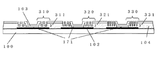
図1に周期構造を持った有機EL発光装置の概略断面図を示す。なお、図示例では有機EL発光装置を示したが、無機EL発光装置やQD−LED発光装置であっても実施できる。 FIG. 1 shows a schematic cross-sectional view of an organic EL light emitting device having a periodic structure. In addition, although the organic EL light-emitting device was shown in the example of illustration, it can implement also with an inorganic EL light-emitting device and a QD-LED light-emitting device.
図1に示した有機EL発光装置を成す有機EL素子(発光素子)は、基板100上に陽極である反射電極(第1電極)102が形成されている。反射電極102の周縁を覆うように絶縁部材から成る素子分離層104が形成されている。この素子分離層104の開口部から露出する反射電極102の露出部上に、蛍光性有機化合物若しくは燐光性有機化合物を含む機能層(有機層)101、陰極である透明電極(第2電極)103が形成されている。
In the organic EL element (light emitting element) constituting the organic EL light emitting device shown in FIG. 1, a reflective electrode (first electrode) 102 that is an anode is formed on a
有機層101は、図3に示すように、通常、ホール輸送層106、発光層105(R発光層115、G発光層125、B発光層135)、電子輸送層107が積層された構成をとる。また、必要に応じて反射電極102とホール輸送層106との間にホール注入層108を、透明電極103と電子輸送層107との間に電子注入層109を挟持しても良い。
As shown in FIG. 3, the
発光層105は、それぞれの発光色に応じた蛍光性有機化合物若しくは燐光性有機化合物を含む。これらの有機EL素子に電圧を印加することで、反射電極102から注入された正孔と透明電極103から注入された電子とが、有機層101において再結合し発光する。ちなみに、本実施形態の有機EL素子は、発光点201に対して透明電極103側が、光取り出し面となる。
The
つまり、上記有機EL発光装置は、通例の有機EL発光装置と略同様の構成とされている。しかし、通例の有機EL発光装置は、図4に示すように、可視光域において、光取り出し側である空気の屈折率1.0と比較して、発光層を含む有機層101の屈折率が約1.6〜2.0程度と大きい。そのため、有機層101側から空気界面に、臨界角以上の角度で入射した光は全反射されてしまう。発光点201から放射される光のうち、約80%が全反射のため導波光203として素子内部に閉じ込められる。伝播光202として素子外部へ取り出される光の割合(光取り出し効率)は、通常、約20%程度でしかない。
That is, the organic EL light emitting device has a configuration substantially similar to that of a normal organic EL light emitting device. However, as shown in FIG. 4, in the usual organic EL light emitting device, the refractive index of the
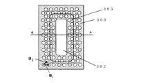
そこで、本発明の有機EL発光装置は、素子分離層104の前記基板100と反対側の面に周期構造300が形成されている。本実施形態の周期構造300は、図2や図16、図17に示すように、EL発光領域302の周辺に2次元的なフォトニック結晶構造をとる。なお、図1の反射電極102、有機層101、透明電極103が積層された部分に対応するのが、図2や図17のEL発光領域302である。
Therefore, in the organic EL light emitting device of the present invention, the
さらに周期構造300の底部と反射電極102との間に光導波路301が形成されている。つまり、反射電極102は光導波路301を形成するために、EL発光領域302だけでなく、周期構造300が形成されている領域まで広がって形成されている。この光導波路301はプレーナー型とされており、周期構造300のエッチングの深さを調整することで形成される。
Further, an
上記構成の有機EL発光装置は、有機層101に閉じ込められた導波光203が、基板101に対して水平方向に伝わり、光導波路301を進行していく。導波光203が光導波路301を進行するに伴い、周期構造300によって光の回折を生じ、伝播方向が光取り出し面方向に曲げられる。その結果、導波光203から回折光204に変換されるため、光取り出し効率が改善され、発光効率が向上する。
In the organic EL light emitting device having the above configuration, the guided
しかも、図1において有機層101の上部や下部に、周期構造を形成する必要がない。そのため、有機層101の形成後の周期構造300の作製プロセスによる前記有機層101の損傷や、周期構造300上への有機層101の形成による膜の不均一性や密着性の低下などによる素子特性や素子耐久の低下を回避することが可能である。
In addition, it is not necessary to form a periodic structure above or below the
さらに、図2に示すように、発光に寄与する領域が、EL発光領域302からその周囲の回折光領域303まで拡大する。以下で詳述するが、回折光領域303はEL発光領域302よりも約10μm程度の幅で周辺部に広がる。そのため、高精細化によりEL発光領域302が小さくなるほど、外周近傍での回折光204の影響が大きくなり、より発光効率が向上される。したがって、高精細化に伴い開口率が低下しても、駆動電流密度の上昇を抑制することが可能で、有機EL素子の耐久性を維持することが可能である。
Furthermore, as shown in FIG. 2, the region contributing to light emission expands from the EL
以下で、周期構造300について考察を行う。図2に示すように、周期構造300の周期を規定する2つの基本格子ベクトルをa1、a2とする。また、これらの基本格子ベクトルa1、a2に対し、数1の関係を満たす基本逆格子ベクトルをb1、b2とする。有機EL素子の有機層101からの発光ピーク波長(すなわち、前記周期構造300を介して外部に取り出される光のスペクトルのピーク波長)をλとし、波数をk=2π/λとする。また、素子分離層104の屈折率をn、光取り出し側媒体(通常は空気)の屈折率をnexとし、条件n>nexを満たすとする。
Hereinafter, the
![]()
![]()
光導波路301を伝播する導波光203に対する基板100の水平方向への伝播係数をβとし、導波光203に対する有効屈折率neff及び有効吸収係数κeffを、数2により定義する。有効屈折率neffは、条件nex<neff<nを満たす。
The propagation coefficient in the horizontal direction of the
![]()
![]()
このとき、回折条件は水平方向の位相整合条件から、2つの整数m1、m2を回折次数とし、基板法線方向に対する回折角度をθ(m1、m2)として、条件nex<neff<nのもとで、数3で与えられる。 At this time, the diffraction condition is the condition n ex <n where the two integers m 1 and m 2 are the diffraction orders and the diffraction angle with respect to the normal direction of the substrate is θ (m 1 , m 2 ) from the phase matching condition in the horizontal direction. It is given by Equation 3 under eff <n.
![]()
![]()
数3から、各(m1、m2)次回折が生じるための条件は、数4を満たす範囲内である。さらに、条件nex<neff<nを用いると、各(m1、m2)次回折が生じるための条件は、概ね数5となる。
From
![]()
![]()
![]()
![]()
周期構造300が図16や図17のような正方格子の場合を考える。図16は凹部分が正方形の場合であり、図17は凸部分が正方形の場合の例である。正方格子の周期をaとすると、基本格子ベクトルa1、a2は数6となり、基本逆格子ベクトルb1、b2は数7となる。
Consider the case where the

この時、数3の回折条件は、数8となる。また、数4で表される各(m1、m2)次回折が生じるための条件は、数9となる。さらに、条件nex<neff<nを用いると、各(m1、m2)次回折が生じるための条件は、概ね数10となる。
At this time, the diffraction condition of
![]()
![]()
![]()
![]()
![]()
![]()
ここで、どちらか一方の1次元方向に着目し、m2=0(若しくは、m1=0)とすれば、m1=|m1|=m>0(若しくは、m2=|m2|=m>0)とする。この時、数8の回折条件は、簡略化され数11となる。また、各m次回折が生じるための周期aは、数12を満たす範囲内である。さらに、条件nex<neff<nを用いると、各m次回折が生じるための周期aの条件は、概ね数13となる。
Here, paying attention to one of the one-dimensional directions and assuming that m 2 = 0 (or m 1 = 0), m 1 = | m 1 | = m> 0 (or m 2 = | m 2 | = M> 0). At this time, the diffraction condition of Equation 8 is simplified and becomes Equation 11. In addition, the period a for generating each m-th order diffraction is in a range satisfying Expression 12. Furthermore, when the condition n ex <n eff <n is used, the condition of the period a for generating each m-th order diffraction is approximately
![]()
![]()
![]()
![]()
![]()
![]()
同様に、数13から、m次回折のみが生じるための周期aは、数14を満たす範囲内である。さらに、条件nex<neff<nを用いると、m次回折のみが生じるための周期aの条件は、概ね数15となる。 Similarly, from equation (13), the period a for generating only m-order diffraction is within a range satisfying equation (14). Furthermore, when the condition n ex <n eff <n is used, the condition of the period a for generating only m-th order diffraction is approximately Equation 15.
![]()
![]()
![]()
![]()
有機EL素子では、通常、素子分離層104の屈折率はn=1.5〜2.5程度、光取り出し側の屈折率nexはnex=1.0〜1.5程度である。よって、数13から回折光204が生じるため、周期構造300の周期aは、概ね発光ピーク波長λの0.25倍より大きいことが望ましい。さらに、主に1次から3次程度の低次回折光を利用する場合には、数15から周期構造300の周期aは、概ね発光ピーク波長λの0.25倍より大きく2.0倍より小さいことが望ましい。可視光の波長域が380nm〜780nmであることから、周期構造300の周期aは、120nmから1200nmであることが望ましい。
In the organic EL element, the refractive index of the
周期構造300は、上述したように2次元的なフォトニック結晶構造に限定されず、図5のように1次元的な回折格子の組み合わせでも良い。また、図6のように一つの副画素に、EL発光領域302が複数存在しても良い。さらに、周期構造300は、周期的である必要はなく、準結晶構造や連続的に周期構造が変化する構造、部分的に不規則な散乱構造を有する構造、若しくは周期構造とこれらを組み合わせたものでも良い。
The
図3のホール輸送層106、発光層105、電子輸送層107、ホール注入層108、電子注入層109に用いられる有機化合物としては、低分子材料、高分子材料若しくはその両方により構成され、特に限定されるものではない。さらに、必要に応じて無機化合物を用いても良い。
The organic compound used for the
なお、これまでは、基板側が陽極となる構成で説明してきたが、基板側が陰極となる積層構成においても本発明を実施することは可能であり、特に限定されるものではない。 Heretofore, the description has been made with the configuration in which the substrate side is the anode, but the present invention can also be implemented in a stacked configuration in which the substrate side is the cathode, and is not particularly limited.
さらに、透明基板上に透明電極を形成し、その上に有機層、反射電極を積層したボトムエミッション構成においても本発明を実施可能である。 Furthermore, the present invention can also be implemented in a bottom emission configuration in which a transparent electrode is formed on a transparent substrate and an organic layer and a reflective electrode are stacked thereon.
また、複数の有機EL素子が積層されたマルチフォトン構成や多段階積層構成に対しても本発明は実施可能である。 In addition, the present invention can be applied to a multi-photon configuration in which a plurality of organic EL elements are stacked or a multistage stacked configuration.
以下、数値計算による評価例及び比較例を示す。電磁波の数値計算には、有機EL発光装置の断面を考え、2次元FDTD法を用いた。 Hereinafter, evaluation examples by numerical calculation and comparative examples will be shown. Considering the cross section of the organic EL light emitting device, the two-dimensional FDTD method was used for the numerical calculation of electromagnetic waves.
<比較例1>
図7に、素子分離層104が周期構造を持たず、光導波路301のみを有する場合の構造を示す。
<Comparative Example 1>
FIG. 7 shows a structure in which the
有機EL素子の発光部分は、基板上に反射電極102(膜厚60nm、屈折率(実部)は0.15及び屈折率(虚部)は3.58)が形成されている。そして、反射電極102上に透明電極110(膜厚20nm、屈折率2.0)、有機層101(膜厚70nm、屈折率1.7)が形成されている。さらに、有機層101上に透明電極103(膜厚60nm、屈折率2.0)が形成された積層構造とした。波長λ=460nm前後の光に対し、基板100の垂直方向で干渉強め合いが生じ、微小共振器構造となるように光路長を設定した。つまり、有機EL素子の積層方向に微小共振器構造を有する構造とした。有機EL素子の側面に配置される素子分離層104は屈折率2.0とした。
In the light emitting portion of the organic EL element, a reflective electrode 102 (film thickness 60 nm, refractive index (real part) is 0.15 and refractive index (imaginary part) is 3.58) is formed on the substrate. A transparent electrode 110 (film thickness 20 nm, refractive index 2.0) and an organic layer 101 (film thickness 70 nm, refractive index 1.7) are formed on the
また、素子分離層104の境界までの距離が1.0μmである有機層101内の発光点201に発光源が存在するとし、発光波長λ=460nmの単色で定常的な同心円状の発光が生ずるとした。電磁波モードはTEモードで計算を行った。
Further, assuming that a light emitting source exists at the
さらに、測定域A(401)、測定域B(402)、測定域C(403)、測定域D(404)を設け、それぞれの測定域を透過するエネルギー量を計算した。 Furthermore, the measurement area A (401), the measurement area B (402), the measurement area C (403), and the measurement area D (404) were provided, and the amount of energy transmitted through each measurement area was calculated.
以上は、各評価例及び比較例1に共通の設定である。 The above is a setting common to each evaluation example and comparative example 1.
比較例1では、素子分離層104の膜厚を150nmとした。図8に、素子分離層104が光導波路301のみを有する場合の数値計算結果を示す。発光点201から放出された光のうち、有機EL素子の外部へ取り出される光は、一部の伝播光202のみであり、残りの大部分が基板の水平方向へ導波光203として閉じ込められてしまうことが理解される。
In Comparative Example 1, the thickness of the
ここで、導波光203の有効屈折率neff及び有効吸収係数κeffを求めた。導波光203の伝播係数βの実部は、図8より約0.0225[1/nm]であった。これから、有効屈折率をneff=約1.65と求めた。
Here, the effective refractive index n eff and the effective absorption coefficient κ eff of the guided
次に、有効吸収係数κeffを求めた。図8のX軸座標で、導波光203の位置X1でのエネルギーをI(X1)、位置X2でのエネルギーをI(X2)とすると、有効吸収係数κeffとの間に数16の関係式が成り立つ。
Next, the effective absorption coefficient κ eff was determined. If the energy at the position X1 of the guided
![]()
![]()
測定域C(403)での透過エネルギー量がI(5μm)=0.0124[a.u]、測定域D(404)での透過エネルギー量がI(3μm)=0.0144[a.u]であったので、数16から有効吸収係数をκeff=約0.0028と求めた。 The amount of transmitted energy in the measurement area C (403) is I (5 μm) = 0.124 [a. u], the transmission energy amount in the measurement area D (404) is I (3 μm) = 0.144 [a. u], the effective absorption coefficient was calculated as κ eff = about 0.0028 from Equation 16.
有効吸収係数κeff=約0.0028より、導波光203のエネルギーが半減するのに要する半減距離Xhalfは9.1μmと求まり、およそ10μmであった。 From the effective absorption coefficient κ eff = about 0.0028, the half distance X half required for the energy of the guided light 203 to be halved is 9.1 μm, which is about 10 μm.
<評価例1>
次に、本発明の発光装置の構成例として、図9に示すように素子分離層104の光導波路301上に周期構造300を形成した場合の数値計算結果を示す。図9は、周期構造の高さhが230nm、周期aが230nmの場合である。この場合の数値計算結果を図10に示す。
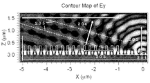
<Evaluation Example 1>
Next, as a structural example of the light emitting device of the present invention, a numerical calculation result when the
位相整合条件である数11に、導波光203の有効屈折率neff=1.65を適応すると、1次回折光のみが発生し回折角度は−20.5度であることがわかった。なお、回折角度は光の導波方向に対して90°より小さい角度方向を正とし、導波方向に対して90°より大きい角度方向を負とする。この位相整合条件から計算された回折角度は、図9の計算結果に示された回折光波面205から求められる回折光204の回折角度と良く整合している。
It was found that when the effective refractive index n eff = 1.65 of the guided
周期構造300の周期aを、115nmから920nmまで115nm間隔で変化させ、伝播光202と回折光204とを合わせた取り出し光に対応する測定域A及び測定域Bを透過するエネルギーを求めた。表1に、周期構造300を有さない比較例1の値を基準にした時の相対値を示す。
The period a of the
周期aが115nmの場合は、回折が生じる条件である数13を満たしておらず、回折光204が発生しない。そのため、光取り出し効率は比較例1とほぼ同じ値である。
In the case where the period a is 115 nm,
一方、周期aが230nmから920nmの場合は、回折効果により光取り出し効率が改善していることがわかった。特に、周期aが460nmから805nmの場合に、取り出し効率の改善効果が大きい。 On the other hand, when the period a was 230 nm to 920 nm, it was found that the light extraction efficiency was improved by the diffraction effect. In particular, when the period a is 460 nm to 805 nm, the effect of improving the extraction efficiency is great.
光取り出し効率が最大となるのは、周期aが690nmの時であった。周期aが690nmの時の数値計算結果を図11に示す。周期aが690nmの場合には、1次から3次の回折光が発生するが、このうち、基板垂直方向に近い18.5度方向に2次回折光が、さらに−20.5度方向に3次回折光が同時に発生するためであると考えられる。 The light extraction efficiency was maximized when the period a was 690 nm. The numerical calculation results when the period a is 690 nm are shown in FIG. When the period a is 690 nm, first-order to third-order diffracted light is generated. Of these, second-order diffracted light in the 18.5 degree direction, which is close to the substrate vertical direction, and 3 in the −20.5 degree direction. This is probably because the next-order diffracted light is generated simultaneously.
<評価例2>
回折による導波光203から回折光204への変換効率は、周期構造300の高さhを変化させることで調整することが可能である。そこで、本発明の発光装置の構成例として、周期構造300の周期aが一定(230nm)の場合に、高さhを115nmから460nmまで変化させ、測定域A及び測定域Bを透過するエネルギーを求めた。表2に、周期構造300を有さない比較例1の値を基準にしたときの相対値を示す。高さhが115nmと460nmの場合に、回折光204が強くなり光取り出し効率が向上することがわかった。
<Evaluation Example 2>
The conversion efficiency from the guided light 203 to the diffracted
<評価例3>
また、導波光203から回折光204への変換効率を制御するには、光導波路301の高さdを調整し、導波光203の有効屈折率neffを変化させることが大変有効である。そこで、本発明の発光装置の構成例として、周期構造の周期aを一定(230nm)として、光導波路301の高さdを150nmから70nmに変化させた場合の測定域A及び測定域Bを透過するエネルギーを求めた。図12に数値計算結果を示す。
<Evaluation Example 3>
In order to control the conversion efficiency from the guided light 203 to the diffracted
光導波路の高さが連続的に変化する構造、即ちチャープ構造304によって、光導波路301の高さdを連続的に低くした構造としている。表3に、光導波路301の高さdを150nm一定の場合、150nmから70nmに変化させた場合、150nmから30nmに変化させた場合に、測定域A及び測定域Bを透過するエネルギーを示す。周期構造300を有さない比較例1の値を基準としている。
The structure in which the height d of the
表3に示した結果より、チャープ構造304を導入し、光導波路301の高さdを低下させることにより、回折光強度が大幅に増加し、光取り出し効率が向上していることがわかった。これは、有効屈折率neffが下限値nexに近づいたことにより、エバネッセント波による光導波路からの染み出しが大きくなり、周期構造の影響を受けやすくなったため、若しくは導波モードが消失したためと考えられる。
From the results shown in Table 3, it was found that by introducing the
比較例1の計算例より、導波光203の半減距離Xhalfは約10μmであった。したがって、導波光203の基板水平方向の伝達距離を半減距離程度と考えると、約10μmとなる。図1に示すように、素子分離層104に周期構造300を設置した場合に、素子分離層上に配置された周期構造の回折効果により取り出せる光は、素子分離層と有機層との境界から約10μm以内がほとんどである。よって、図2において、回折光領域303の拡大範囲も境界から約10μm程度である。
From the calculation example of Comparative Example 1, the half distance X half of the guided
図2のEL発光領域302の面積が非常に大きい場合には、周辺部の取り出し効率向上の寄与は相対的に小さい。逆に、150ppiから300ppi程度の高精細化に伴い、副画素サイズが百数十μmから数十μm四方に微細化されると、周辺部の取り出し効率向上の寄与が大きくなり、発光効率を向上させることが可能となる。また、図6のように1つの副画素に、EL発光領域302を複数存在させることで、周辺部の寄与を増加させ、発光効率を向上させることもできる。
When the area of the EL
一般に、表示装置では、視認性を良くするために高コントラストが要求される。特に、小型ディスプレイなどのような屋外での利用が多い表示装置では、コントラストを保つために外光反射防止機能が大変重要である。有機EL表示装置に対する有効な反射防止方法としては、円偏光板の設置や共振器干渉打ち消し効果とカラーフィルターを組み合わせた方法がある。しかしながら、いずれも平面構造を有する有機EL表示装置に対し有効な方法であるため、光取り出し効率を向上させるために周期構造や回折格子を配置すると、反射防止性能が低下してしまう。そのため、反射防止機能を維持する構造を有することが望ましい。 In general, a display device is required to have high contrast in order to improve visibility. In particular, in a display device that is frequently used outdoors, such as a small display, an external light reflection preventing function is very important for maintaining contrast. As an effective antireflection method for an organic EL display device, there are a method in which a circular polarizing plate is installed and a resonator interference canceling effect is combined with a color filter. However, since both are effective methods for an organic EL display device having a planar structure, if a periodic structure or a diffraction grating is disposed in order to improve the light extraction efficiency, the antireflection performance is degraded. Therefore, it is desirable to have a structure that maintains the antireflection function.
以下、図18、図19、図20により、本発明の表示装置に対して、外光反射防止機能を保有させる構造例について説明を行う。 Hereinafter, a structural example in which the display device of the present invention has an external light reflection preventing function will be described with reference to FIGS.
図18に示すように、本発明において、表示装置の周期構造上方部分にブラックマトリックス501を配置し、さらに、その上部に円偏光板502を配置する。表示装置が複数の発光素子を有している場合には、発光素子の周囲に形成された周期構造は隣り合う発光素子の間に形成されることになる。そして、ブラックマトリックスも隣り合う発光素子の間に形成される。
As shown in FIG. 18, in the present invention, a
発光点201からの伝播光202は、ブラックマトリックス501の開口部から表示装置外部に放射される。また、外部に取り出したい波長において、回折光204は、ブラックマトリックス501の開口部から外部に放射されるように、光導波路中の導波光203に対して負の回折角度であることが望ましい。ここで、負の回折角度とは、導波光203の導波方向に対して、90°より大きい角度を有することである。さらに、周期構造を介して外部に取り出される光が、光導波路の導波方向に対して90°より大きい角度方向で最大強度若しくは最大輝度となることが望ましい。
Propagated light 202 from the
回折光が負の回折角度となる条件は、数3の回折条件より、以下のようになる。つまり、周期構造を介して外部に取り出したい光のスペクトルのピーク波長をλ、2つの整数m1、m2を回折次数、基板法線方向に対する回折角度をθ(m1、m2)として、条件nex<neff<nのもとで、概ね数17で与えられる。
The conditions under which the diffracted light has a negative diffraction angle are as follows based on the diffraction conditions of
![]()
![]()
また、正方格子の場合に回折光が負の回折角度となる条件は、正方格子の周期をaとして、数8の回折条件から、概ね数18で与えられる。 Further, the condition that the diffracted light has a negative diffraction angle in the case of a square grating is given by Equation 18 from the diffraction condition of Equation 8 with the period of the square lattice being a.
![]()
![]()
図19に、本発明の表示装置に、外光が垂直に近い角度で入射する場合の概略図を示す。入射光(垂直近傍)210のうち、EL発光領域への入射光は、円偏光板により反射光が防止される。また、周期構造の上方部への入射光は、ブラックマトリックスによって反射が防止される。 FIG. 19 shows a schematic diagram when external light is incident on the display device of the present invention at an angle close to vertical. Of the incident light (near vertical) 210, the incident light to the EL light emitting region is prevented from being reflected by the circularly polarizing plate. Also, the incident light on the upper part of the periodic structure is prevented from being reflected by the black matrix.
次に、図20に、本発明の表示装置に、外光が斜め方向から入射する場合の概略図を示す。 Next, FIG. 20 shows a schematic diagram when external light is incident on the display device of the present invention from an oblique direction.
斜め入射光222は、円偏光板を透過し円偏光となり、その後、周期構造に反射して斜め反射光223となる。斜め反射光223は、周期構造によって円偏光状態から楕円偏光となるが、ブラックマトリックスによって吸収されるため、反射が防止される。 The oblique incident light 222 passes through the circularly polarizing plate and becomes circularly polarized light, and then is reflected by the periodic structure to become obliquely reflected light 223. Although the obliquely reflected light 223 changes from a circularly polarized state to an elliptically polarized light due to the periodic structure, it is absorbed by the black matrix, and thus reflection is prevented.
以上から、周期構造を配置して光取り出し効率を向上させると同時に、外光入射に対する反射光を低減することが可能である。 As described above, it is possible to improve the light extraction efficiency by arranging the periodic structure, and at the same time, it is possible to reduce the reflected light with respect to external light incidence.
同様に、図21、図22、図23に、本発明の表示装置に対して、外光反射防止機能を保有させる他の構成例を示す。 Similarly, FIGS. 21, 22 and 23 show other configuration examples in which the display device of the present invention has an external light reflection preventing function.
図21において、表示装置を構成するEL発光素子は、発光色がR(赤)の赤色発光素子(以下R素子とする)であり、赤色を強める共振器素子(R共振器素子)とする。表示装置の周期構造の上方部分にブラックマトリックス501を配置し、さらに、ブラックマトリックスの開口部に赤色光を透過するカラーフィルター(Rカラーフィルター)513を配置する。光の取り出しに関しては、図18の場合と同様である。
In FIG. 21, an EL light-emitting element constituting the display device is a red light-emitting element (hereinafter referred to as an R element) whose emission color is R (red), and is a resonator element (R resonator element) that enhances red. A
図22に、本発明の表示装置に、外光が垂直に近い角度で入射する場合の概略図を示す。入射光(垂直近傍)210のうち、EL発光領域への入射光は、Rカラーフィルター513により、赤色の透過光(R透過光)213と成る。共振器では、共振器中の干渉強め合い条件と反射光への干渉打ち消し条件が、概ね一致する。そのため、赤色(R発光色)を強めるR共振器素子では、R透過光213に対して、R共振器素子の各界面からの赤色の反射光(R反射光)214Aや214Bなどが干渉打ち消しを起こし、反射を抑えることができる。また、周期構造の上方部への入射光は、ブラックマトリックスによって反射が防止される。
FIG. 22 shows a schematic diagram when external light is incident on the display device of the present invention at an angle close to vertical. Of the incident light (near the vertical) 210, the incident light to the EL light emitting region becomes red transmitted light (R transmitted light) 213 by the R color filter 513. In the resonator, the interference strengthening condition in the resonator and the interference canceling condition for the reflected light substantially coincide. Therefore, in the R resonator element that enhances red (R emission color), the red reflected light (R reflected light) 214A and 214B from each interface of the R resonator element cancels interference with the R transmitted
図23に示す外光が斜め方向から入射する場合は、図20の場合と同様である。R(赤)について説明を行ったが、G(緑)やB(青)の場合も同様である。 The case where the external light shown in FIG. 23 is incident from an oblique direction is the same as the case of FIG. Although R (red) has been described, the same applies to G (green) and B (blue).
なお、これまでは、基板側を陽極、光取り出し側を陰極とする構成で説明してきたが、基板側を陰極、光取り出し側を陽極とし、ホール輸送層、発光層、電子輸送層を逆順に積層した構成においても本発明を実施することは可能である。したがって、本発明にかかる表示装置は基板側を陽極、光取り出し側を陰極とする構成に限定されるものではない。 In the above description, the substrate side is the anode and the light extraction side is the cathode. However, the substrate side is the cathode, the light extraction side is the anode, and the hole transport layer, light emitting layer, and electron transport layer are in reverse order. The present invention can be implemented even in a stacked configuration. Therefore, the display device according to the present invention is not limited to the configuration in which the substrate side is an anode and the light extraction side is a cathode.
さらに、図24に示すように、透明基板上に透明電極を形成し、その上に有機層、反射性電極を積層したボトムエミッション構成においても本発明を実施可能である。この場合、光導波路301は反射性電極部分を除く周期構造の底部と基板(透明電極103と基板100の界面)との間である。
Furthermore, as shown in FIG. 24, the present invention can also be implemented in a bottom emission configuration in which a transparent electrode is formed on a transparent substrate and an organic layer and a reflective electrode are laminated thereon. In this case, the
また、光取り出し側の電極を透明電極とする構成で説明してきたが、図15に示すように、光取り出し側の電極を金属半透明電極193とする構成においても本発明を実施可能である。この場合、光導波路は金属半透明電極193部分を除く周期構造300の底部と反射性電極102との間である。
Further, although the configuration in which the light extraction side electrode is a transparent electrode has been described, the present invention can also be implemented in a configuration in which the light extraction side electrode is a metal
さらに、この構成では、金属半透明電極193と素子分離層104(若しくはRGB共通有機層)との界面を基板水平方向に伝播する導波光の一種と考えることができる表面プラズモンが生じる。よって、金属半透明電極193と素子分離層104(若しくはRGB共通有機層)との界面を光導波路として利用可能である。表面プラズモンの伝播係数βSPを、数2の伝播係数βとすると、通常の導波光と同様に回折条件は数3で与えられる。
Furthermore, in this configuration, surface plasmons that can be considered as a kind of guided light propagating in the horizontal direction of the substrate at the interface between the metal
以上、本発明の発光装置の実施の形態について説明したが、本発明の発光装置は、表示装置や、照明、表示装置用のバックライト等の様々な用途に適用することができる。表示装置としては、テレビ受像機、パーソナルコンピュータのディスプレイ、撮像装置の背面表示部、携帯電話の表示部、携帯ゲーム機の表示部、携帯音楽再生装置の表示部、携帯情報端末(PDA)の表示部、カーナビゲーションシステムの表示部等がある。 Although the embodiments of the light emitting device of the present invention have been described above, the light emitting device of the present invention can be applied to various uses such as a display device, illumination, and a backlight for the display device. As a display device, a television receiver, a display of a personal computer, a rear display unit of an imaging device, a display unit of a mobile phone, a display unit of a portable game machine, a display unit of a portable music player, a display of a personal digital assistant (PDA) And a display unit of a car navigation system.
以下、本発明の発光装置の製造方法を実施例として説明するが、本発明は本実施例によって何ら限定されるものではない。 Hereinafter, although the manufacturing method of the light-emitting device of this invention is demonstrated as an Example, this invention is not limited at all by this Example.
<実施例1>
図13に示す構成のフルカラー有機EL発光装置を以下に示す方法で作製する。つまり、本実施例の発光装置は、複数の画素を有し、各画素が赤色発光素子、緑色発光素子、青色発光素子、つまり赤、緑、青の3色の副画素からなる有機EL発光装置であって、表示装置として好ましく適用することができる例である。以下、赤色発光素子をR素子、緑色発光素子をG素子、青色発光素子をB素子とする。
<Example 1>
A full-color organic EL light-emitting device having the configuration shown in FIG. 13 is manufactured by the following method. That is, the light-emitting device of this embodiment has a plurality of pixels, and each pixel is a red light-emitting element, a green light-emitting element, and a blue light-emitting element, that is, an organic EL light-emitting apparatus composed of three sub-pixels of red, green, and blue. In this example, the display device can be preferably applied. Hereinafter, a red light emitting element is an R element, a green light emitting element is a G element, and a blue light emitting element is a B element.
まず、支持体としてのガラス基板100上に、低温ポリシリコンからなるTFT駆動回路を形成し、その上にアクリル樹脂からなる平坦化膜を形成して基板とする。この上に反射性金属としてのAg合金(AgPdCu)をスパッタリング法にて約100nmの膜厚で形成してパターニングし、透明導電膜としてのIZOをスパッタリング法にて20nmの膜厚で形成してパターニングし、反射電極102とする。Ag合金からなる反射電極102は、可視光の波長域(λ=380nm〜780nm)で分光反射率80%以上の高反射電極である。
First, a TFT drive circuit made of low-temperature polysilicon is formed on a
さらに、SiNxOy(酸化窒化珪素)の素子分離層104を320nmの膜厚で形成した後、各副画素に図2に示すようなEL発光領域302と三角格子の周期構造310(320、330)とのエッチングを行い、フォトニック結晶付き陽極基板を作製する。
Further, after forming an
ここで、EL発光領域302は50μm四方とする。本実施例では、R素子の周期構造(R周期構造)310は周期930nm、エッチング直径620nm、エッチング深さ180nmとされる。G素子の周期構造(G周期構造)320は周期795nm、エッチング直径530nm、エッチング深さ210nmとされる。B素子の周期構造(B周期構造)330は周期690nm、エッチング直径460nm、エッチング深さ230nmとされる。つまり、周期構造の周期は、R素子が最も長く、B素子が最も短い。
Here, the
これをイソプロピルアルコール(IPA)で超音波洗浄し、次いで、煮沸洗浄後乾燥する。その後、UV/オゾン洗浄してからR素子、G素子、B素子それぞれの有機層111、121、131を真空蒸着により形成する。 This is subjected to ultrasonic cleaning with isopropyl alcohol (IPA) and then dried after boiling and drying. Then, after UV / ozone cleaning, the organic layers 111, 121, and 131 of the R element, G element, and B element are formed by vacuum deposition.
まず、下記構造式で示される化合物[I]を、シャドーマスクを用いて各副画素に、R素子のホール輸送層として50nmの膜厚、G素子のホール輸送層として30nmの膜厚、B素子のホール輸送層として20nmの膜厚で形成する。この際の真空度は1×10⁻⁴Pa、蒸着レートは0.2nm/secである。 First, compound [I] represented by the following structural formula is applied to each sub-pixel using a shadow mask, with a film thickness of 50 nm as a hole transport layer of an R element, a film thickness of 30 nm as a hole transport layer of a G element, and a B element. The hole transport layer is formed with a thickness of 20 nm. The degree of vacuum at this time is 1 × 10 −4 Pa and the deposition rate is 0.2 nm / sec.
次に、発光層として、シャドーマスクを用いて、R素子、G素子、B素子それぞれの発光層を形成する。R素子の発光層としては、ホストとして4,4’−Bis(N‐carbazole)biphenyl(以下、CBPと呼ぶ)と、燐光発光性化合物Bis[2−(2’−benzothienyl)pyridinato−N,C3](acetylacetonato)Iridium(以下、Btp2Ir(acac)と呼ぶ)とを共蒸着して60nmの膜厚で発光層を形成する。G素子の発光層としては、ホストとしてtris−(8−hydroxyquinoline)Aluminum(以下、Alq3と呼ぶ)と、発光性化合物として3−(2’−Benzothiazolyl)−7−N,N−diethylaminocoumarin(以下、クマリン6と呼ぶ)とを共蒸着して40nmの膜厚で発光層を形成する。B素子の発光層としては、ホストとして下記に示す化合物[II]と発光性化合物[III]とを共蒸着して20nmの膜厚で発光層を形成する。蒸着時の真空度は1×10⁻⁴Pa、成膜速度は0.2nm/secである。 Next, as the light emitting layer, the light emitting layers of the R element, the G element, and the B element are formed using a shadow mask. As the light-emitting layer of the R element, 4,4′-Bis (N-carbazole) biphenyl (hereinafter referred to as CBP) and phosphorescent compound Bis [2- (2′-benzothienyl) pyridinato-N, C3 are used as a host. ] (Acetylacetonato) Iridium (hereinafter referred to as Btp2Ir (acac)) is co-evaporated to form a light emitting layer with a thickness of 60 nm. As a light emitting layer of the G element, tris- (8-hydroxyquinoline) Aluminum (hereinafter referred to as Alq3) as a host and 3- (2′-Benzothiazolyl) -7-N, N-diethylaminocoumarin (hereinafter referred to as a light emitting compound) as a light emitting compound. And co-evaporated to form a light emitting layer with a thickness of 40 nm. As the light emitting layer of the B element, a compound [II] and a light emitting compound [III] shown below are co-deposited as a host to form a light emitting layer with a thickness of 20 nm. The degree of vacuum during vapor deposition is 1 × 10 −4 Pa, and the film formation rate is 0.2 nm / sec.
さらに、共通の電子輸送層として、1、10−Bathophenanthroline(以下、BPhenと呼ぶ)を真空蒸着法にて10nmの膜厚で一括して形成する。蒸着時の真空度は1×10⁻⁴Pa、成膜速度は0.2nm/secである。次に、共通の電子注入層として、BPhenとCs2CO3とを共蒸着(重量比90:10)し、20nmの膜厚で一括して形成する。蒸着時の真空度は3×10-4Pa、成膜速度は0.2nm/secである。 Furthermore, as a common electron transport layer, 1,10-Bathophanethroline (hereinafter referred to as BPhen) is collectively formed with a film thickness of 10 nm by a vacuum deposition method. The degree of vacuum during vapor deposition is 1 × 10 −4 Pa, and the film formation rate is 0.2 nm / sec. Next, as a common electron injection layer, BPhen and Cs 2 CO 3 are co-evaporated (weight ratio 90:10) and are collectively formed to a thickness of 20 nm. The degree of vacuum during vapor deposition is 3 × 10 −4 Pa, and the film formation rate is 0.2 nm / sec.
この電子注入層まで形成した基板を、真空を破ること無しにスパッタ装置に移動し、透明電極103として、ITOを60nmの膜厚で形成する。
The substrate formed up to the electron injection layer is moved to a sputtering apparatus without breaking the vacuum, and ITO is formed to a thickness of 60 nm as the
その結果、素子分離層104には、周期構造310(320、330)の底部と反射電極102との間に光導波路311(321、331)が形成される。ここで、素子分離層104に形成された周期構造310上には、R素子、G素子、B素子の間を跨いで共通して形成される共通層が積層されることになる。図1や図13では、透明電極のみ示すが、実施例1では、電子輸送層、電子注入層、透明電極が順次積層される。ここで、透明電極103の屈折率や有機層111(121、131)の屈折率は素子分離層104の屈折率と概ね等しいことが好ましい。素子分離層104に積層された透明電極103を前記素子分離層104と同一の部材とみなし、周期構造310(320、330)及び光導波路311(321、331)を形成することができるからである。
As a result, in the
さらに、発光装置の周辺部に吸湿剤を配置し、エッチングされたキャップガラスで封止することにより、有機EL発光装置を得る。 Furthermore, an organic EL light emitting device is obtained by disposing a hygroscopic agent in the periphery of the light emitting device and sealing with an etched cap glass.
<実施例2>
図14に実施例2の有機EL発光装置の構成図を示す。ホール輸送層の形成前までは、実施例1と同様である。化合物[I]を各副画素に、R素子のホール輸送層として70nmの膜厚、G素子のホール輸送層として40nmの膜厚、B素子のホール輸送層として20nmの膜厚で形成する。次に、共通の3色積層型白色(W)発光層として、CBPとBis[(4,6−difluorophenyl)pyridinato−N,C2](picolinato)Iridium(以下、FIrpicと呼ぶ)とを共蒸着により25nmの膜厚で形成する。そして、CBPとBtp2Ir(acac)(重量比92:8)とを共蒸着により2nmの膜厚で形成する。さらに、CBPとBis(2−phenylbenzothiozolato−N−C2)Iridium(acetylacetonate)(以下、Bt2Ir(acac)と呼ぶ)(重量比92:8)とを共蒸着により2nmの膜厚で形成し積層構造とする。電子輸送層の形成以降は、実施例1と同様である。
<Example 2>
FIG. 14 shows a configuration diagram of an organic EL light-emitting device of Example 2. Before the formation of the hole transport layer, the process is the same as in Example 1. Compound [I] is formed in each subpixel with a film thickness of 70 nm as the hole transport layer of the R element, a film thickness of 40 nm as the hole transport layer of the G element, and a film thickness of 20 nm as the hole transport layer of the B element. Next, CBP and Bis [(4,6-difluorophenyl) pyridinato-N, C2] (picolinato) Iridium (hereinafter referred to as FIrpic) are co-deposited as a common three-color laminated white (W) light emitting layer. It is formed with a film thickness of 25 nm. Then, CBP and Btp2Ir (acac) (weight ratio 92: 8) are formed to a thickness of 2 nm by co-evaporation. Further, CBP and Bis (2-phenylbenzothiolato-N-C2) Iridium (aceylatetonate) (hereinafter referred to as Bt2Ir (acac)) (weight ratio 92: 8) are formed to a thickness of 2 nm by co-evaporation. To do. After the formation of the electron transport layer, the process is the same as in Example 1.
つまり、本実施例の有機EL発光装置は各副画素にW有機層171が形成されており、白色の有機EL素子を有する構成とされている。 In other words, the organic EL light-emitting device of this example has a configuration in which the W organic layer 171 is formed in each sub-pixel and has a white organic EL element.
<実施例3>
図15に実施例3の有機EL発光装置の構成図を示す。電子注入層の形成までは、実施例1と同様である。この電子注入層まで形成した基板を、真空を破ること無しにスパッタ装置に移動し、金属半透明電極193として、Ag合金を20nmの膜厚で形成する。
<Example 3>
FIG. 15 shows a configuration diagram of an organic EL light-emitting device of Example 3. The process up to the formation of the electron injection layer is the same as in Example 1. The substrate formed up to the electron injection layer is moved to a sputtering apparatus without breaking the vacuum, and an Ag alloy is formed with a thickness of 20 nm as the metal
さらに、発光装置の周辺部に吸湿剤を配置し、エッチングされたキャップガラスで封止することにより、有機EL発光装置を得る。 Furthermore, an organic EL light emitting device is obtained by disposing a hygroscopic agent in the periphery of the light emitting device and sealing with an etched cap glass.
つまり、本実施例の有機EL発光装置は各副画素にR素子の有機層111、G素子の有機層121、B素子の有機層131が形成されており、金属半透明電極を有する構成とされている。 In other words, the organic EL light-emitting device of this example has an R element organic layer 111, a G element organic layer 121, and a B element organic layer 131 formed in each sub-pixel, and has a metal translucent electrode. ing.
<実施例4>
本実施例は、図13に示す構成のフルカラー有機EL発光装置において、素子分離層104に形成される周期構造が、図16に示す正方格子である場合である。反射電極の形成までは、実施例1と同様である。
<Example 4>
In this example, in the full color organic EL light emitting device having the configuration shown in FIG. 13, the periodic structure formed in the
さらに、SiNxOy(酸化窒化珪素)の素子分離層104を175nmの膜厚で形成した後、各副画素に図16に示すようなEL発光領域302と正方格子の周期構造310(320、330)とのエッチングを行い、フォトニック結晶付き陽極基板を作製する。
Further, after forming an
ここで、EL発光領域302は50μm四方とする。正方格子では、各副画素の上下方向と左右方向とで周期構造310(320、330)の周期(配列)が等しい。そのため、発光装置を視認した場合、上下方向と左右方向とで同様の光学特性を得ることができ、視認性を高めることができる。また、逆に、上下方向と左右方向の周期が異なる四角格子としても良い。この場合は、方向によって視認性を調整することが可能となる。
Here, the
本実施例では、R周期構造310は周期310nm、エッチング形状が一辺220nm正方形、エッチング深さ40nmとされる。G周期構造320は周期270nm、エッチング形状が一辺190nm正方形、エッチング深さ90nmとされる。B周期構造330は周期230nm、エッチング形状が一辺150nm正方形、エッチング深さ115nmとされる。つまり、周期構造の周期は、R素子が最も長く、B素子が最も短い。
In this embodiment, the R
これをイソプロピルアルコール(IPA)で超音波洗浄し、次いで、煮沸洗浄後乾燥する。その後、UV/オゾン洗浄してからR素子、G素子、B素子それぞれの有機層111、121、131を真空蒸着により形成する。 This is subjected to ultrasonic cleaning with isopropyl alcohol (IPA) and then dried after boiling and drying. Then, after UV / ozone cleaning, the organic layers 111, 121, and 131 of the R element, G element, and B element are formed by vacuum deposition.
まず、化合物[I]を、シャドーマスクを用いて各副画素に、R素子のホール輸送層として25nmの膜厚、G素子のホール輸送層として25nmの膜厚、B素子のホール輸送層として20nmの膜厚で形成する。この際の真空度は1×10⁻⁴Pa、蒸着レートは0.2nm/secである。 First, compound [I] is applied to each sub-pixel using a shadow mask, with a film thickness of 25 nm as the hole transport layer of the R element, a film thickness of 25 nm as the hole transport layer of the G element, and 20 nm as the hole transport layer of the B element. The film thickness is formed. The degree of vacuum at this time is 1 × 10 −4 Pa and the deposition rate is 0.2 nm / sec.
次に、発光層として、シャドーマスクを用いて、R素子、G素子、B素子それぞれの発光層を形成する。R素子の発光層としては、ホストとしてCBPと、燐光発光性化合物Btp2Ir(acac)とを共蒸着して50nmの膜厚で発光層を形成する。G素子の発光層としては、ホストとしてAlq3と、発光性化合物クマリン6とを共蒸着して30nmの膜厚で発光層を形成する。B素子の発光層としては、ホストとして化合物[II]と発光性化合物[III]とを共蒸着して20nmの膜厚で発光層を形成する。蒸着時の真空度は1×10⁻⁴Pa、成膜速度は0.2nm/secである。 Next, as the light emitting layer, the light emitting layers of the R element, the G element, and the B element are formed using a shadow mask. As the light emitting layer of the R element, CBP as a host and phosphorescent compound Btp2Ir (acac) are co-evaporated to form a light emitting layer with a thickness of 50 nm. As the light emitting layer of the G element, Alq3 as a host and the light emitting compound coumarin 6 are co-evaporated to form a light emitting layer with a thickness of 30 nm. As the light emitting layer of the B element, compound [II] and light emitting compound [III] are co-evaporated as a host to form a light emitting layer with a thickness of 20 nm. The degree of vacuum during vapor deposition is 1 × 10 −4 Pa, and the film formation rate is 0.2 nm / sec.
次に、共通の電子輸送層として、BPhenを真空蒸着法にて10nmの膜厚で一括して形成する。蒸着時の真空度は1×10⁻⁴Pa、成膜速度は0.2nm/secである。 Next, as a common electron transport layer, BPhen is collectively formed with a film thickness of 10 nm by a vacuum deposition method. The degree of vacuum during vapor deposition is 1 × 10 −4 Pa, and the film formation rate is 0.2 nm / sec.
さらに、BPhenとCs2CO3との共蒸着膜(重量比90:10)を、シャドーマスクを用いて各副画素に、R素子の電子注入層として60nmの膜厚、G素子の電子注入層として30nmの膜厚、B素子の電子注入層として20nmの膜厚で形成する。蒸着時の真空度は3×10⁻⁴Pa、成膜速度は0.2nm/secである。透明電極103の形成以降は、実施例1と同様である。
Further, a co-deposited film (weight ratio of 90:10) of BPhen and Cs 2 CO 3 is applied to each sub-pixel using a shadow mask, with a film thickness of 60 nm as the electron injection layer of the R element, and the electron injection layer of the G element. As an electron injection layer of the B element, a film thickness of 20 nm is formed. The degree of vacuum during vapor deposition is 3 × 10 −4 Pa, and the film formation rate is 0.2 nm / sec. The processes after the formation of the
100 基板
101 有機層
102 反射電極
103 透明電極
104 素子分離層
105 発光層
106 ホール輸送層
107 電子輸送層
108 ホール注入層
109 電子注入層
110 反射電極上の透明電極
111 R有機層
115 R発光層
121 G有機層
125 G発光層
131 B有機層
135 B発光層
171 W有機層
193 金属半透明電極
201 発光点
202 伝播光
203 導波光
204 回折光
205 回折光波面
210 入射光(垂直近傍)
211 透過光(左円偏光)
212 反射光(右円偏光)
213 R透過光
214A R反射光A
214B R反射光B
222 斜め入射光
223 斜め反射光
300 周期構造
301 光導波路
302 EL発光領域
303 回折光領域
304 チャープ構造
310 R周期構造
311 R光導波路
320 G周期構造
321 G光導波路
330 B周期構造
331 B光導波路
401 測定域A
402 測定域B
403 測定域C
404 測定域D
501 ブラックマトリックス
502 円偏光板
513 Rカラーフィルター
DESCRIPTION OF
211 Transmitted light (left circularly polarized light)
212 Reflected light (right circularly polarized light)
213 R transmitted light 214A R reflected light A
214B R reflected light B
222 oblique incident light 223 oblique reflected light 300
402 Measurement area B
403 Measurement area C
404 Measurement area D
501 Black Matrix 502 Circular Polarizer 513 R Color Filter
Claims (12)
前記発光素子は、前記基板の上に形成されている第1電極と、前記第1電極の周縁を覆っている絶縁部材と、前記第1電極の露出部の上に形成されており、少なくとも発光層を有する機能層と、前記機能層及び前記絶縁部材の上に形成されている第2電極とを有する発光装置において、
前記絶縁部材の前記基板と反対側の面には周期構造が形成されており、前記周期構造の底部と前記第1電極、若しくは前記周期構造の底部と基板との間に光導波路が形成されていることを特徴とする発光装置。 A substrate, and a light emitting element formed on the substrate,
The light emitting element is formed on a first electrode formed on the substrate, an insulating member covering a periphery of the first electrode, and an exposed portion of the first electrode, and at least emits light. In a light emitting device having a functional layer having a layer and a second electrode formed on the functional layer and the insulating member,
A periodic structure is formed on the surface of the insulating member opposite to the substrate, and an optical waveguide is formed between the bottom of the periodic structure and the first electrode, or between the bottom of the periodic structure and the substrate. A light emitting device characterized by comprising:
前記周期構造の周期は、前記赤色発光の発光素子が最も長く、前記青色発光の発光素子が最も短いことを特徴とする請求項1乃至請求項3のいずれか1項に記載の発光装置。 The light emitting element emitting red light, the light emitting element emitting green light, and the light emitting element emitting blue light,
4. The light emitting device according to claim 1, wherein a period of the periodic structure is the longest for the red light emitting element and the shortest for the blue light emitting element. 5.
Priority Applications (2)
| Application Number | Priority Date | Filing Date | Title |
|---|---|---|---|
| JP2008011088A JP2009044117A (en) | 2007-02-09 | 2008-01-22 | Light-emitting device |
| US12/028,107 US7868542B2 (en) | 2007-02-09 | 2008-02-08 | Light-emitting apparatus having periodic structure and sandwiched optical waveguide |
Applications Claiming Priority (3)
| Application Number | Priority Date | Filing Date | Title |
|---|---|---|---|
| JP2007030476 | 2007-02-09 | ||
| JP2007187796 | 2007-07-19 | ||
| JP2008011088A JP2009044117A (en) | 2007-02-09 | 2008-01-22 | Light-emitting device |
Publications (2)
| Publication Number | Publication Date |
|---|---|
| JP2009044117A true JP2009044117A (en) | 2009-02-26 |
| JP2009044117A5 JP2009044117A5 (en) | 2011-02-03 |
Family
ID=40444483
Family Applications (1)
| Application Number | Title | Priority Date | Filing Date |
|---|---|---|---|
| JP2008011088A Withdrawn JP2009044117A (en) | 2007-02-09 | 2008-01-22 | Light-emitting device |
Country Status (1)
| Country | Link |
|---|---|
| JP (1) | JP2009044117A (en) |
Cited By (8)
| Publication number | Priority date | Publication date | Assignee | Title |
|---|---|---|---|---|
| JP2010272214A (en) * | 2009-05-19 | 2010-12-02 | Fuji Electric Holdings Co Ltd | Color conversion type organic el display |
| WO2011114424A1 (en) * | 2010-03-15 | 2011-09-22 | パイオニア株式会社 | Organic el panel and method for producing same |
| WO2012147390A1 (en) * | 2011-04-28 | 2012-11-01 | 昭和電工株式会社 | Organic light-emitting element, production method for organic light-emitting element, display device, and illumination device |
| JP2013524438A (en) * | 2010-03-31 | 2013-06-17 | ゼネラル・エレクトリック・カンパニイ | Light emitting device and article |
| KR20150078953A (en) * | 2013-12-31 | 2015-07-08 | 삼성디스플레이 주식회사 | Organic light-emitting display apparatus |
| US9356079B2 (en) | 2014-06-19 | 2016-05-31 | Samsung Display Co., Ltd. | Organic light-emitting display apparatus and method of manufacturing the same |
| US9774003B2 (en) | 2012-09-03 | 2017-09-26 | Idemitsu Kosan Co., Ltd. | Organic electroluminescent element and electronic instrument |
| JP2017530539A (en) * | 2014-09-05 | 2017-10-12 | 京東方科技集團股▲ふん▼有限公司Boe Technology Group Co.,Ltd. | Organic light emitting diode display panel, manufacturing method thereof, and display device |
-
2008
- 2008-01-22 JP JP2008011088A patent/JP2009044117A/en not_active Withdrawn
Cited By (11)
| Publication number | Priority date | Publication date | Assignee | Title |
|---|---|---|---|---|
| JP2010272214A (en) * | 2009-05-19 | 2010-12-02 | Fuji Electric Holdings Co Ltd | Color conversion type organic el display |
| WO2011114424A1 (en) * | 2010-03-15 | 2011-09-22 | パイオニア株式会社 | Organic el panel and method for producing same |
| JP2013524438A (en) * | 2010-03-31 | 2013-06-17 | ゼネラル・エレクトリック・カンパニイ | Light emitting device and article |
| KR20180030957A (en) * | 2010-03-31 | 2018-03-26 | 보에 테크놀로지 그룹 컴퍼니 리미티드 | Light-emitting device and article |
| WO2012147390A1 (en) * | 2011-04-28 | 2012-11-01 | 昭和電工株式会社 | Organic light-emitting element, production method for organic light-emitting element, display device, and illumination device |
| US9774003B2 (en) | 2012-09-03 | 2017-09-26 | Idemitsu Kosan Co., Ltd. | Organic electroluminescent element and electronic instrument |
| KR20150078953A (en) * | 2013-12-31 | 2015-07-08 | 삼성디스플레이 주식회사 | Organic light-emitting display apparatus |
| KR102086557B1 (en) | 2013-12-31 | 2020-03-10 | 삼성디스플레이 주식회사 | Organic light-emitting display apparatus |
| US9356079B2 (en) | 2014-06-19 | 2016-05-31 | Samsung Display Co., Ltd. | Organic light-emitting display apparatus and method of manufacturing the same |
| US9640782B2 (en) | 2014-06-19 | 2017-05-02 | Samsung Display Co., Ltd. | Organic light-emitting display apparatus and method of manufacturing the same |
| JP2017530539A (en) * | 2014-09-05 | 2017-10-12 | 京東方科技集團股▲ふん▼有限公司Boe Technology Group Co.,Ltd. | Organic light emitting diode display panel, manufacturing method thereof, and display device |
Similar Documents
| Publication | Publication Date | Title |
|---|---|---|
| US7868542B2 (en) | Light-emitting apparatus having periodic structure and sandwiched optical waveguide | |
| JP5219493B2 (en) | Light emitting element and light emitting device using the same | |
| US8304788B2 (en) | Display apparatus and method of producing same | |
| US8304796B2 (en) | Light-emitting apparatus | |
| US20230094133A1 (en) | Enhanced oled outcoupling by suppressing surface plasmon modes | |
| JP2009044117A (en) | Light-emitting device | |
| US20110213094A1 (en) | Anionic Water-Soluble Additives Based on Allyl Ether and Vinyl Ether | |
| US20100123384A1 (en) | Tiled oled device with edge light extraction | |
| JP2006108093A (en) | Organic light-emitting element and method for manufacturing the same | |
| JP2005063838A (en) | Optical device and organic el display device | |
| WO2017043242A1 (en) | Organic electroluminescence device, lighting device and display device | |
| KR20090089151A (en) | Organic light emitting diode display and method for manufacturing the same | |
| WO2017086306A1 (en) | Organic electroluminescence device, organic electroluminescence device production method, illumination device, and display device | |
| WO2017043243A1 (en) | Organic electroluminescence device, organic electroluminescence device manufacturing method, lighting device and display device | |
| KR20130113642A (en) | Substrate for oled with enhanced light extraction efficiency, method for fabricating thereof and oled having the same | |
| JP2008226718A (en) | Organic el device | |
| JP5562379B2 (en) | ORGANIC LIGHT EMITTING ELEMENT AND LIGHT EMITTING DEVICE AND DISPLAY DEVICE USING THE SAME | |
| JP2013073800A (en) | Display device | |
| JP2005276662A (en) | Light emitting display device | |
| CN110646980B (en) | Liquid crystal display | |
| WO2016043175A1 (en) | Organic electroluminescent device and method for producing electroluminescent device | |
| JP4286216B2 (en) | Luminescent display device | |
| JP2009272194A (en) | Light-emitting device | |
| JP2010287562A (en) | Display device | |
| WO2009064021A1 (en) | Display apparatus and method of producing same |
Legal Events
| Date | Code | Title | Description |
|---|---|---|---|
| A521 | Request for written amendment filed |
Free format text: JAPANESE INTERMEDIATE CODE: A523 Effective date: 20101213 |
|
| A621 | Written request for application examination |
Free format text: JAPANESE INTERMEDIATE CODE: A621 Effective date: 20101213 |
|
| A761 | Written withdrawal of application |
Free format text: JAPANESE INTERMEDIATE CODE: A761 Effective date: 20120125 |