JP5465088B2 - Organic electroluminescence device - Google Patents
Organic electroluminescence device Download PDFInfo
- Publication number
- JP5465088B2 JP5465088B2 JP2010123733A JP2010123733A JP5465088B2 JP 5465088 B2 JP5465088 B2 JP 5465088B2 JP 2010123733 A JP2010123733 A JP 2010123733A JP 2010123733 A JP2010123733 A JP 2010123733A JP 5465088 B2 JP5465088 B2 JP 5465088B2
- Authority
- JP
- Japan
- Prior art keywords
- layer
- light emitting
- exciton
- emitting layer
- fluorescent light
- Prior art date
- Legal status (The legal status is an assumption and is not a legal conclusion. Google has not performed a legal analysis and makes no representation as to the accuracy of the status listed.)
- Expired - Fee Related
Links
Images


Classifications
-
- H—ELECTRICITY
- H10—SEMICONDUCTOR DEVICES; ELECTRIC SOLID-STATE DEVICES NOT OTHERWISE PROVIDED FOR
- H10K—ORGANIC ELECTRIC SOLID-STATE DEVICES
- H10K50/00—Organic light-emitting devices
- H10K50/10—OLEDs or polymer light-emitting diodes [PLED]
- H10K50/11—OLEDs or polymer light-emitting diodes [PLED] characterised by the electroluminescent [EL] layers
- H10K50/12—OLEDs or polymer light-emitting diodes [PLED] characterised by the electroluminescent [EL] layers comprising dopants
- H10K50/121—OLEDs or polymer light-emitting diodes [PLED] characterised by the electroluminescent [EL] layers comprising dopants for assisting energy transfer, e.g. sensitization
-
- H—ELECTRICITY
- H05—ELECTRIC TECHNIQUES NOT OTHERWISE PROVIDED FOR
- H05B—ELECTRIC HEATING; ELECTRIC LIGHT SOURCES NOT OTHERWISE PROVIDED FOR; CIRCUIT ARRANGEMENTS FOR ELECTRIC LIGHT SOURCES, IN GENERAL
- H05B33/00—Electroluminescent light sources
- H05B33/12—Light sources with substantially two-dimensional radiating surfaces
- H05B33/14—Light sources with substantially two-dimensional radiating surfaces characterised by the chemical or physical composition or the arrangement of the electroluminescent material, or by the simultaneous addition of the electroluminescent material in or onto the light source
-
- H—ELECTRICITY
- H10—SEMICONDUCTOR DEVICES; ELECTRIC SOLID-STATE DEVICES NOT OTHERWISE PROVIDED FOR
- H10K—ORGANIC ELECTRIC SOLID-STATE DEVICES
- H10K50/00—Organic light-emitting devices
- H10K50/10—OLEDs or polymer light-emitting diodes [PLED]
- H10K50/11—OLEDs or polymer light-emitting diodes [PLED] characterised by the electroluminescent [EL] layers
- H10K50/125—OLEDs or polymer light-emitting diodes [PLED] characterised by the electroluminescent [EL] layers specially adapted for multicolour light emission, e.g. for emitting white light
- H10K50/13—OLEDs or polymer light-emitting diodes [PLED] characterised by the electroluminescent [EL] layers specially adapted for multicolour light emission, e.g. for emitting white light comprising stacked EL layers within one EL unit
- H10K50/131—OLEDs or polymer light-emitting diodes [PLED] characterised by the electroluminescent [EL] layers specially adapted for multicolour light emission, e.g. for emitting white light comprising stacked EL layers within one EL unit with spacer layers between the electroluminescent layers
-
- H—ELECTRICITY
- H10—SEMICONDUCTOR DEVICES; ELECTRIC SOLID-STATE DEVICES NOT OTHERWISE PROVIDED FOR
- H10K—ORGANIC ELECTRIC SOLID-STATE DEVICES
- H10K59/00—Integrated devices, or assemblies of multiple devices, comprising at least one organic light-emitting element covered by group H10K50/00
-
- H—ELECTRICITY
- H10—SEMICONDUCTOR DEVICES; ELECTRIC SOLID-STATE DEVICES NOT OTHERWISE PROVIDED FOR
- H10K—ORGANIC ELECTRIC SOLID-STATE DEVICES
- H10K2101/00—Properties of the organic materials covered by group H10K85/00
- H10K2101/10—Triplet emission
-
- H—ELECTRICITY
- H10—SEMICONDUCTOR DEVICES; ELECTRIC SOLID-STATE DEVICES NOT OTHERWISE PROVIDED FOR
- H10K—ORGANIC ELECTRIC SOLID-STATE DEVICES
- H10K2101/00—Properties of the organic materials covered by group H10K85/00
- H10K2101/27—Combination of fluorescent and phosphorescent emission
-
- H—ELECTRICITY
- H10—SEMICONDUCTOR DEVICES; ELECTRIC SOLID-STATE DEVICES NOT OTHERWISE PROVIDED FOR
- H10K—ORGANIC ELECTRIC SOLID-STATE DEVICES
- H10K2101/00—Properties of the organic materials covered by group H10K85/00
- H10K2101/40—Interrelation of parameters between multiple constituent active layers or sublayers, e.g. HOMO values in adjacent layers
Description
本発明は、一対の電極間に少なくとも発光層を含む有機化合物層を有する有機EL(エレクトロルミネッセンス)素子に関する。 The present invention relates to an organic EL (electroluminescence) device having an organic compound layer including at least a light emitting layer between a pair of electrodes.
近年、有機EL素子を用いた発光装置、或いは表示装置が盛んに研究開発されている。一般的に、有機EL素子は2つの電極と、これら電極間にある発光層を含む有機化合物層とによって構成されている。この発光層の発光材料としては、蛍光材料と燐光材料がある。 In recent years, light-emitting devices or display devices using organic EL elements have been actively researched and developed. In general, an organic EL element is composed of two electrodes and an organic compound layer including a light emitting layer between these electrodes. As the light emitting material of the light emitting layer, there are a fluorescent material and a phosphorescent material.
燐光材料は、蛍光材料に比べて原理的に高発光効率が期待できる。何故ならば、キャリア再結合により生成される励起子は一重項励起子と三重項励起子からなり、その確率は1:3である。一重項励起子を利用した有機EL素子は、一重項励起子から基底状態に遷移する際の蛍光を発光として取り出していたが、原理的にその発光収率は生成された励起子数に対して、25%であり、これが原理的上限であった。しかしながら、三重項励起子から基底状態に遷移する際の燐光を発光として利用すれば、原理的に少なくとも3倍の収率が期待できる。さらに、エネルギー的に高い一重項から三重項への項間交差による転移を考え合わせれば、原理的には4倍の100%の発光収率が期待できる。このため、青色、緑色、赤色を発する燐光材料の開発が進められている。 In principle, phosphorescent materials can be expected to have higher luminous efficiency than fluorescent materials. This is because excitons generated by carrier recombination are composed of singlet excitons and triplet excitons, and the probability is 1: 3. The organic EL device using singlet excitons has taken out the fluorescence at the time of transition from the singlet exciton to the ground state as luminescence, but in principle the luminescence yield is the number of excitons generated. 25%, which was the theoretical upper limit. However, if phosphorescence at the transition from the triplet exciton to the ground state is used as light emission, a yield of at least 3 times can be expected in principle. Furthermore, if considering the transition due to the intersystem crossing from singlet to triplet in terms of energy, in principle, a light emission yield of 100%, which is four times, can be expected. For this reason, the development of phosphorescent materials that emit blue, green, and red is underway.
しかし現状では、青色の燐光材料において、実用に足る寿命が得られていない。このため、フルカラーディスプレイや白色照明用途において、燐光材料による良好な電力効率を呈する有機EL素子の実用化を阻んでいる。 However, at present, a blue phosphorescent material does not have a practical life. For this reason, practical use of the organic EL element which exhibits the favorable power efficiency by a phosphorescent material is prevented in a full color display or white illumination use.
この状況を克服し得る手段として、青色蛍光材料と、緑色から赤色帯域の燐光材料とを組み合わせることにより、原理的に100%に近い発光量子収率が期待できる有機EL素子が提案されている(非特許文献1、特許文献1)。 As a means for overcoming this situation, an organic EL element that can expect a light emission quantum yield close to 100% in principle by combining a blue fluorescent material and a phosphor material in a green to red band has been proposed ( Non-patent document 1, Patent document 1).
以下に、非特許文献1に提案されている有機EL素子の概要を述べる。この有機EL素子では、発光層となるホスト材料層中に、蛍光材料ドープ領域と燐光材料ドープ領域とが分離して形成されており、該発光層中の蛍光材料ドープ領域でキャリアを再結合させて励起子を偏在させて生成する。この時、25%は一重項励起子になり、75%は三重項励起子になる。一重項励起子はフェルスター機構でエネルギー移動して、蛍光材料の一重項を励起し、蛍光材料は直ちに失活して蛍光発光する。一方、三重項励起子はフェルスター機構ではスピン禁制のためエネルギー移動できず、ホスト中を拡散して燐光材料ドープ領域に達する。ここで、燐光材料分子と接触してデクスター機構で燐光材料の三重項を励起し、この後燐光材料は失活して燐光発光する。これにより、発生させた励起子を高い比率で発光に寄与させることが可能となる。 Below, the outline | summary of the organic EL element proposed by the nonpatent literature 1 is described. In this organic EL device, a fluorescent material doped region and a phosphorescent material doped region are separately formed in a host material layer that becomes a light emitting layer, and carriers are recombined in the fluorescent material doped region in the light emitting layer. Thus, excitons are unevenly distributed. At this time, 25% become singlet excitons and 75% become triplet excitons. Singlet excitons transfer energy by the Forster mechanism to excite singlet of the fluorescent material, and the fluorescent material immediately deactivates and emits fluorescence. On the other hand, triplet excitons cannot be transferred due to spin forbidden in the Förster mechanism and diffuse in the host to reach the phosphorescent material doped region. Here, the triplet of the phosphorescent material is excited by the Dexter mechanism in contact with the phosphorescent material molecule, and then the phosphorescent material is deactivated to emit phosphorescence. Thereby, the generated excitons can be contributed to light emission at a high ratio.
尚、蛍光材料ドープ領域と燐光材料ドープ領域とは、フェルスター機構の及ぶ範囲(フェルスター半径)以上に隔離させておく。このように隔離しておけば、蛍光材料の一重項が励起された後に燐光材料の一重項にエネルギー移動してしまったり、蛍光材料ドープ領域に形成された励起子から直接燐光材料の一重項を励起してしまったりして、蛍光発光が行なわれなくなることを防止できる。 It should be noted that the fluorescent material doped region and the phosphorescent material doped region are separated from the range covered by the Förster mechanism (Förster radius). If isolated in this way, energy transfer to the singlet of the phosphorescent material after the singlet of the fluorescent material is excited, or the singlet of the phosphorescent material directly from the excitons formed in the fluorescent material doped region. It is possible to prevent the fluorescence from being lost due to excitation.
しかしながら、非特許文献1のような有機EL素子においても、発光せずに熱失活してしまう経路を完全には排除できていない。その理由は、蛍光材料ドープ領域で励起子を生成しているため、三重項励起子が、燐光材料ドープ領域まで拡散して行く前に、蛍光材料と接触してデクスター機構により蛍光材料の三重項を励起してしまう確率が一定の割合で存在するからである。蛍光材料の三重項を励起してしまうと、従来の蛍光材料を用いた発光層と同様に、そのエネルギーは熱失活して無駄になってしまう。 However, even in an organic EL element such as Non-Patent Document 1, a path that is thermally deactivated without emitting light cannot be completely eliminated. The reason for this is that excitons are generated in the fluorescent material doped region, so that the triplet excitons come into contact with the fluorescent material before diffusing to the phosphorescent material doped region, and the triplet of the fluorescent material by the Dexter mechanism. This is because there is a certain ratio that excites. When the triplet of the fluorescent material is excited, the energy is wasted due to heat deactivation as in the light emitting layer using the conventional fluorescent material.
蛍光材料のドープ量を少なくすることで、上述のような蛍光三重項励起の割合を低減させることができるが、蛍光材料のドープ量の低減は、一重項励起エネルギーが蛍光材料に移動せずに失活する比率を増大させてしまう。そのため、白色を発光させる場合には、蛍光材料が担当している発光帯域の色成分が減少し、白色の色度が劣化してしまう。また、ドープする蛍光材料を三重項エネルギーの高い材料にして、三重項励起子をトラップし難いようにすることも可能である。しかしながら、この場合、蛍光一重項エネルギーも高くなって励起され難くなるので、やはり一重項励起エネルギーが蛍光材料に移動せずに失活する比率を増大させてしまう。 By reducing the doping amount of the fluorescent material, the ratio of the fluorescence triplet excitation as described above can be reduced. However, the reduction of the doping amount of the fluorescent material does not cause the singlet excitation energy to move to the fluorescent material. It will increase the rate of deactivation. Therefore, when white light is emitted, the color component of the light emission band that the fluorescent material is responsible for decreases, and the white chromaticity deteriorates. It is also possible to make it difficult to trap triplet excitons by making the fluorescent material to be doped a material having high triplet energy. However, in this case, since the fluorescence singlet energy becomes high and is difficult to be excited, the rate at which the singlet excitation energy is deactivated without moving to the fluorescent material is also increased.
本発明の課題は、上記問題点に鑑み、蛍光材料と燐光材料とを用いて、発光量子収率の高い有機EL素子を提供することを目的とする。 In view of the above problems, an object of the present invention is to provide an organic EL device having a high emission quantum yield using a fluorescent material and a phosphorescent material.
本発明は、一対の電極と、前記一対の電極の間に挟持された、発光領域を含む有機化合物層とを有する有機エレクトロルミネッセンス素子であって、
前記発光領域が、少なくとも蛍光性発光層と燐光性発光層と、前記蛍光性発光層と燐光性発光層との間に配置された、自身では発光せずに励起子の生成のみが行なわれる励起子生成層とで構成され、
前記蛍光性発光層と前記励起子生成層との間に励起子防止層が挿入されており、前記励起子防止層と前記励起子生成層との間にキャリアのエネルギー障壁界面が存在し、前記エネルギー障壁界面の前記励起子生成層側にキャリアが蓄積されて励起子が生成されることを特徴とする。
The present invention is an organic electroluminescence device having a pair of electrodes and an organic compound layer including a light emitting region sandwiched between the pair of electrodes,
The light emitting region is disposed at least between the fluorescent light emitting layer and the phosphorescent light emitting layer, and between the fluorescent light emitting layer and the phosphorescent light emitting layer, and excitation that generates only excitons without emitting light itself. Child generation layer,
An exciton prevention layer is inserted between the fluorescent light emitting layer and the exciton generation layer, and an energy barrier interface of carriers exists between the exciton prevention layer and the exciton generation layer , Excitons are generated by accumulating carriers on the exciton generation layer side of the energy barrier interface.
本発明によれば、良好な電力効率を呈し、且つ寿命の長い有機EL素子を提供することが可能となり、従来よりも消費電力の更なる低減ができる。 ADVANTAGE OF THE INVENTION According to this invention, it becomes possible to provide the organic EL element which exhibits favorable power efficiency and has a long lifetime, and can further reduce power consumption compared with the past.
以下、本発明の実施の形態を図面に基づいて説明する。 Hereinafter, embodiments of the present invention will be described with reference to the drawings.
本発明の有機エレクトロルミネッセンス素子(EL素子)は、一対の電極と、該電極間に挟持された有機化合物層とを有し、該有機化合物層は発光領域を含んでいる。そして、該発光領域は、少なくとも蛍光性発光層と燐光性発光層と、該蛍光性発光層と燐光性発光層との間に配置された、自身では発光せずに励起子の生成のみが行なわれる励起子生成層とを有している。本発明においては、蛍光性発光層と励起子生成層との間に、キャリアのエネルギー障壁界面が存在し、該界面の励起子生成層側にキャリアが蓄積されて励起子が生成される。よって、本発明の有機EL素子を用いて、従来よりも長寿命、低消費電力の発光装置、或いは高品質表示の表示装置を提供することができる。また、白色素子とする場合に、白色の色度を向上させることができる。また、本発明によれば、純粋な燐光材料で構成された素子と比較して、三重項−三重項消滅が抑制され、駆動電流密度の増加に伴う量子効率の低下が抑制される効果がある。 The organic electroluminescence element (EL element) of the present invention has a pair of electrodes and an organic compound layer sandwiched between the electrodes, and the organic compound layer includes a light emitting region. The light-emitting region is disposed at least between the fluorescent light-emitting layer and the phosphorescent light-emitting layer, and between the fluorescent light-emitting layer and the phosphorescent light-emitting layer. And an exciton generation layer. In the present invention, an energy barrier interface of carriers exists between the fluorescent light-emitting layer and the exciton generation layer, and carriers are accumulated on the exciton generation layer side of the interface to generate excitons. Therefore, by using the organic EL element of the present invention, it is possible to provide a light emitting device having a longer life and lower power consumption than the conventional one, or a display device with high quality display. Moreover, when it is set as a white element, white chromaticity can be improved. In addition, according to the present invention, triplet-triplet annihilation is suppressed as compared with an element made of a pure phosphorescent material, and an effect of suppressing a decrease in quantum efficiency accompanying an increase in driving current density is obtained. .
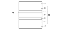
本発明のEL素子の層構成として、例えば図1に示すような構成例が挙げられる。本例では、有機化合物層11を陽極12と陰極13とで挟んだ構造を有する。陽極12と陰極13は、光取り出し側が少なくとも透明電極であり、他方は透明電極或いは反射電極で構成される。尚、本発明における反射電極とは、電極自身が反射性を有する材料からなるものに限らず、ITO,IZOなどの透明導電性材料からなる導電膜の下部に反射性金属等からなる反射性の薄膜を積層したものも含んでそう呼称する。有機化合物層11は、ホール輸送層21、蛍光性発光層22、励起子生成層23、燐光性発光層24、電子輸送層25を順次積層した構成を成す。必要に応じて陽極12とホール輸送層21の間にホール注入層を、陰極13と電子輸送層25の間に電子注入層を狭持しても良い。
As a layer structure of the EL element of the present invention, for example, a structure example as shown in FIG. In this example, the
この素子の陽極12と陰極13の間で電流を流すと、陽極12からホールが、陰極13から電子が注入され、励起子生成層23でホールと電子が再結合して励起子が生成される。ここで、蛍光性発光層22と励起子生成層23との界面31が、後述するように電子のエネルギー障壁になるように蛍光性発光層22と励起子生成層23の材料を選択しておく。これにより、励起子生成層23中を移動してきた電子がこの部位に蓄積され、励起子生成層23内の蛍光性発光層22側に偏った部位で再結合が多く起こる励起子生成領域が形成されることになる。
When a current is passed between the
生成された励起子の内、一重項励起子は、隣接した蛍光性発光層22にドープされている蛍光材料にフェルスター機構でエネルギー移動して、蛍光一重項を励起して蛍光発光を生じさせる。一方、三重項励起子はスピン禁制のため蛍光材料へはエネルギー移動できず、デクスター機構によるエネルギー伝達で拡散して行き、燐光性発光層24に進入して燐光三重項を励起して燐光発光を生じさせる。このようにして、生成された励起子を無駄なく発光に寄与させることができる。
Among the generated excitons, the singlet excitons transfer energy by the Forster mechanism to the fluorescent material doped in the adjacent fluorescent
ここで、蛍光性発光層22の三重項励起エネルギーを、励起子生成層23の三重項励起エネルギーよりも大きくしておくことにより、三重項励起子が蛍光性発光層22に進入するのを効果的に防止できる。
Here, by making the triplet excitation energy of the fluorescent
更に、蛍光性発光層22での励起子生成をより効果的に防止するために、本発明においては、蛍光性発光層22と励起子生成層23との間に励起子防止層(不図示)を挿入する。図1の構成に励起子防止層を組み込むと、励起子防止層と励起子生成層23との界面は電子のエネルギー障壁となって電子が蓄積され、界面近傍に励起子生成領域が形成される。図1の素子においては、電子の蓄積される励起子生成層23側に励起子が生成されるが、一部の電子が障壁界面を抜けて逆側の界面近傍にも励起子が生成されることも起こり得る。この場合、励起子防止層が挿入されていないと、蛍光性発光層22に励起子が生成されることになり、蛍光材料の三重項の励起、熱失活に繋がってしまう。しかしながら、励起子防止層を挿入し、三重項励起エネルギーを励起子生成層23よりも高くしておけば、励起子防止層内に生成された三重項励起子は励起子生成層23側に拡散するので、蛍光材料の三重項の励起を防止できる。
Further, in order to more effectively prevent exciton generation in the fluorescent
更に、蛍光性発光層22の三重項励起エネルギーを励起子防止層よりも大きくしておけば、励起子防止層内に生成された三重項励起子が蛍光性発光層22に進入できず、蛍光三重項の励起をより確実に防止できる。
Furthermore, if the triplet excitation energy of the fluorescent
尚、図1の例では、蛍光性発光層22と励起子生成層23との界面31が電子のエネルギー障壁になるように材料を選択したが、本発明ではこれに限定されない。例えば、図2に示すように、積層順を本例と逆に、燐光性発光層24/励起子生成層23/蛍光性発光層22として、蛍光性発光層22と励起子生成層23との界面32が、ホールのエネルギー障壁となるように構成しても、本発明は同様に機能する。
In the example of FIG. 1, the material is selected so that the
更に、図3に示すように、蛍光性発光層22/励起子生成層23/燐光性発光層24/励起子生成層26/蛍光性発光層27と積層することも可能である。係る構成では、蛍光性発光層22/励起子生成層23の界面31を電子のエネルギー障壁になるようにして、励起子生成層26/蛍光性発光層27の界面32をホールのエネルギー障壁になるようにする。
Furthermore, as shown in FIG. 3, it is also possible to laminate with the fluorescent
本発明では、燐光材料の一重項励起を防止するために、励起子生成領域を励起子生成層23,26の、蛍光性発光層22,27との間のキャリア障壁界面31,32近傍に集中させて形成する。そしてさらには、励起子生成領域を燐光性発光層24からフェルスター半径以上隔離させるようにするのが望ましい。励起子の集中が不充分で燐光性発光層24に近接した部位でも励起子が生成された場合、一重項励起子の一部が燐光材料にエネルギー移動して消費されることになり、蛍光材料の発光色成分が減少する点で好ましくない。しかしその場合でも、励起された燐光一重項は項間交差により燐光三重項に遷移して燐光発光に寄与することになるので、生成された励起子を無駄なく発光に寄与させることは可能である。
In the present invention, in order to prevent singlet excitation of the phosphorescent material, the exciton generation region is concentrated near the carrier barrier interfaces 31 and 32 between the exciton generation layers 23 and 26 and the fluorescent light-emitting
上記構成の各層に用いられる有機化合物は、低分子材料、高分子材料もしくはその両方により構成される。さらに、必要に応じて無機化合物を用いても良い。 The organic compound used for each layer having the above structure is formed of a low molecular material, a high molecular material, or both. Furthermore, you may use an inorganic compound as needed.
以下に本発明の有機EL素子の有機化合物層11の構成に用いることが可能な化合物の具体例を挙げるが、本発明はこれらに限定されるものではない。
Although the specific example of the compound which can be used for the structure of the
ホール輸送層21を構成するホール輸送性材料としては、陽極12からのホールの注入を容易にし、また注入されたホールを発光領域に輸送するに優れたモビリティを有することが好ましい。ホール注入輸送性能を有する低分子及び高分子系材料としては、トリアリールアミン誘導体、フェニレンジアミン誘導体、トリアゾール誘導体、オキサジアゾール誘導体、イミダゾール誘導体、ピラゾリン誘導体、ピラゾロン誘導体が挙げられる。さらに、オキサゾール誘導体、フルオレノン誘導体、ヒドラゾン誘導体、スチルベン誘導体、フタロシアニン誘導体、ポルフィリン誘導体、及びポリ(ビニルカルバゾール)、ポリ(シリレン)、ポリ(チオフェン)、その他導電性高分子が挙げられる。尚、本発明ではこれらに限定されるものではない。以下に、具体例の一部を示す。
The hole transporting material constituting the

発光領域を構成する層のうち、蛍光性発光層22,27及び燐光性発光層24は、ホスト材料中にドーパントとして蛍光性及び燐光性の発光材料をそれぞれ微量ドープした構成を取るのが望ましい。この場合、蛍光性発光層22,27、燐光性発光層24のHOMO準位エネルギー、LUMO準位エネルギーは、ホスト材料のHOMO準位エネルギー、LUMO準位エネルギーとする。また、蛍光性発光層22,27と燐光性発光層24とに挟まれる励起子生成層23,26としては、燐光性発光層24のホストに用いる材料と同様の材料を用いることができる。蛍光性発光層22,27のホスト材料は、励起子生成層23,26との間にキャリアのエネルギー障壁を形成するために、LUMO(最低空軌道)もしくはHOMO(最高被占軌道)のレベルが、励起子生成層とは大きく異なる材料を選択することが要求される。具体的には、蛍光性発光層が励起子生成層よりも陽極側にある場合には、電子のエネルギー障壁を形成するために、蛍光性発光層のLUMO準位エネルギーが励起子生成層のLUMO準位エネルギーよりも小さい材料を用いる。また、蛍光性発光層が励起子生成層よりも陰極側にある場合には、ホールのエネルギー障壁を形成するために、励起子生成層のHOMO準位エネルギーが蛍光性発光層のHOMO準位エネルギーよりも小さい材料を用いる。好ましくは、HOMO準位エネルギー(LUMO準位エネルギー)の差の絶対値が0.2eV以上であり、さらに好ましくは0.3eV以上である。尚、LUMO準位エネルギー,HOMOエネルギー準位は、絶対値で表される。また、励起子生成層23,26中に生成された三重項励起子が蛍光性発光層22,27内に拡散するのを防止するために、蛍光性発光層22,27には励起子生成層23,26よりも三重項励起エネルギーの大きな材料を選択するのが望ましい。但し、励起子防止層を挿入する場合は、励起子防止層の材料としてこの要求を満たす材料を選択しておけば、蛍光性発光層22,27のホスト材料は比較的自由に選択できる。
Of the layers constituting the light-emitting region, the fluorescent light-emitting
尚、本発明において有機化合物層11が上述のようなホスト−ゲスト系で構成される場合、その層のHOMO・LUMOレベルや励起エネルギーは、ホスト材料の値である。以下に発光領域を構成する各層に用いられる材料の具体例の一部を示す。
In the present invention, when the
蛍光性発光層22のホスト及びこれに隣接する励起子防止層の材料としては、例えば、前記したホール輸送性材料と同様の材料が挙げられる。また、蛍光性発光層27のホスト及びこれに隣接する励起子防止層の材料としては、後述する電子輸送性材料と同様の材料を用いることができる。
Examples of the material of the host of the fluorescent
電子輸送層25を構成する電子輸送性材料としては、注入された電子を発光領域に輸送する機能を有するものから任意に選ぶことができ、ホール輸送性材料のキャリア移動度とのバランス等を考慮し選択される。電子注入輸送性能を有する材料としては、オキサジアゾール誘導体、オキサゾール誘導体、チアゾール誘導体、チアジアゾール誘導体、ピラジン誘導体、トリアゾール誘導体、トリアジン誘導体、ペリレン誘導体、キノリン誘導体が挙げられる。また、キノキサリン誘導体、フルオレノン誘導体、アントロン誘導体、フェナントロリン誘導体、有機金属錯体等が挙げられる。尚、本発明においては、これらに限定されるものではない。以下に、具体例の一部を示す。
The electron transporting material constituting the
本発明において、ホール輸送層21と陽極12との間にホール注入層を配置する場合に、該ホール注入層を構成するホール注入材料としては、MoO3,WO3,V2O5等の遷移金属酸化物や、銅フタロシアニン(CuPc)等が挙げられる。また、本発明において、電子輸送層25と陰極13との間に電子注入層を配置する場合に、該電子注入層を構成する電子注入材料としては、アルカリ金属やアルカリ土類金属、もしくはその化合物等が挙げられる。これら電子注入材料は、前述した電子輸送性材料に、0.1質量%以上数十質量%以下含有させることにより、電子注入性を付与することが出来る。電子注入層は、必要不可欠な層ではないが、この後に、陰極13を形成する際の成膜時に受けるダメージを考慮すると、良好な電子注入性を確保するために10nm以上100nm以下程度の厚さで挿入した方が好ましい。
In the present invention, when a hole injection layer is disposed between the
有機化合物層11は、一般に真空蒸着法、イオン化蒸着法、スパッタリング、プラズマにより形成する。また、適当な溶媒に溶解させて、公知の塗布法(例えば、スピンコーティング、ディッピング、キャスト法、LB(ラングミュア−ブロジェット)法、インクジェット法等)により形成することもできる。特に塗布法で成膜する場合は、適当な結着樹脂と組み合わせて膜を形成することもできる。上記結着樹脂としては、広範囲な結着樹脂より選択でき、例えば、ポリビニルカルバゾール樹脂、ポリカーボネート樹脂、ポリエステル樹脂、ポリアリレート樹脂、ポリスチレン樹脂、ABS樹脂、ポリブタジエン樹脂、ポリウレタン樹脂が挙げられる。また、アクリル樹脂、メタクリル樹脂、ブチラール樹脂、ポリビニルアセタール樹脂、ポリアミド樹脂、ポリイミド樹脂、ポリエチレン樹脂、ポリエーテルスルホン樹脂、ジアリルフタレート樹脂、フェノール樹脂、エポキシ樹脂、シリコーン樹脂が挙げられる。また、ポリスルホン樹脂、尿素樹脂等が挙げられるが、これらに限定されるものではない。また、これらは単独または共重合体ポリマーとして1種または2種以上混合してもよい。さらに必要に応じて、公知の可塑剤、酸化防止剤、紫外線吸収剤等の添加剤を併用してもよい。
The
陰極13を透明電極とする場合には、ITOやIZO等の酸化物導電膜を使用することができ、電子輸送層25や電子注入層との組み合わせにより、電子注入性が良好な組み合わせを適宜選択することが望ましい。また、透明電極は、スパッタリングにより形成することができる。
When the
本発明において、必要に応じて、酸素や水分等との接触を防止する目的で保護層が設けられる。保護層としては、窒化シリコン、窒化酸化シリコン等の金属窒化物膜や、酸化タンタル等の金属酸化物膜、ダイヤモンド薄膜、また、フッ素樹脂、ポリパラキシレン、ポリエチレン、シリコーン樹脂、ポリスチレン樹脂等の高分子膜、光硬化性樹脂等が挙げられる。また、ガラス、気体不透過性フィルム、金属などをカバーし、適当な封止樹脂により素子自体をパッケージングすることもできる。また、防湿性を高める為に、保護層内に吸湿材を含有させても良い。 In the present invention, if necessary, a protective layer is provided for the purpose of preventing contact with oxygen, moisture and the like. Protective layers include metal nitride films such as silicon nitride and silicon nitride oxide, metal oxide films such as tantalum oxide, diamond thin films, and high levels of fluorine resin, polyparaxylene, polyethylene, silicone resin, polystyrene resin, etc. Examples thereof include a molecular film and a photocurable resin. Further, it is possible to cover glass, a gas impermeable film, a metal, etc., and to package the element itself with an appropriate sealing resin. Moreover, in order to improve moisture-proof property, you may contain a hygroscopic material in a protective layer.
尚、これまでは、基板側が陽極12となる構成で説明してきたが、基板側が陰極13となる積層構成においても本発明を実施することは可能であり、特に限定されるものではない。さらに、透明基板上に透明電極を形成し、その上に有機化合物層11、反射電極を積層したボトムエミッション構成においても本発明を実施可能である。更にまた、陽極12と陰極13を共に透明電極とすることも可能である。
Heretofore, the description has been made with the configuration in which the substrate side is the
以下、具体的な実施例を挙げて本発明を更に詳細に説明するが、本発明はこれらの実施例に限定されるものではない。尚、以下に記載するHOMO,LUMOとはHOMO,LUMOのエネルギー準位を意味し、絶対値で示す。 Hereinafter, the present invention will be described in more detail with specific examples, but the present invention is not limited to these examples. In addition, HOMO and LUMO described below mean the energy levels of HOMO and LUMO, and are indicated by absolute values.
<参考実施例1>
図3に示す有機EL素子において、陰極13と電子輸送層25との間に電子注入層(不図示)を配置した構成の有機EL素子を以下に示す方法で作製した。
< Reference Example 1>
In the organic EL device shown in FIG. 3, an organic EL device having a configuration in which an electron injection layer (not shown) is disposed between the
先ず、支持体としてのガラス基板上に、反射性金属としてのAg合金(AgPdCu)を約100nmの厚さでスパッタリング法にて形成してパターニングした。さらにその上に、透明導電膜としてのITOをスパッタリング法にて厚さ20nmで形成してパターニングして、反射電極としての陽極12を形成した。さらに、アクリル樹脂により素子分離膜を形成し、陽極付き基板を作成した。これをイソプロピルアルコール(IPA)で超音波洗浄し、次いで、煮沸洗浄後乾燥した。その後、UV/オゾン洗浄してから、以下の有機化合物層11及び陰極13を1×10-4Paの真空チャンバー内で抵抗加熱により真空蒸着し、連続成膜した。
First, an Ag alloy (AgPdCu) as a reflective metal was formed with a thickness of about 100 nm on a glass substrate as a support by a sputtering method and patterned. Further thereon, ITO as a transparent conductive film was formed by sputtering with a thickness of 20 nm and patterned to form an
ホール輸送層21として、TPDを35nmの膜厚に成膜した後、同じTPDをホストとして、蛍光材料である前記フルオレン化合物1を6質量%ドープした蛍光性発光層22を5nmの膜厚に成膜した。次に、励起子生成層23としてCBPを15nmの膜厚に成膜した後、同じCBPをホストとして、燐光材料であるIr(ppy)3を5質量%ドープした燐光性発光層24を20nmの膜厚に成膜した。引き続き、励起子生成層26としてCBPを15nmの膜厚に成膜した。ここで、ホール輸送層21と蛍光性発光層22のホスト材料を同じにしたのは、この2つの層の界面でのホールのエネルギー障壁を低減するためである。
As the
次に、Bphenをホストとして、蛍光材料であるフルオレン化合物1を6質量%ドープした蛍光性発光層27を5nmの膜厚に成膜した後、同じBphenを用いて電子輸送層25を15nmの膜厚に形成した。更に、電子注入層(図示せず)として、BphenとCs2CO3を共蒸着(質量比90:10)し、20nmの膜厚に形成した。ここで、電子輸送層25と蛍光性発光層27のホスト材料を同じにしたのは、この2つの層の界面でのホールのエネルギー障壁を低減するためである。
Next, a fluorescent light-emitting
この電子注入層まで成膜した基板を、真空を破ること無しにスパッタ装置に移動させ、透明電極である陰極13としてITOを60nm成膜し、さらに保護膜として、窒化酸化シリコンを700nmの厚さに成膜した。
The substrate on which the electron injection layer has been formed is moved to a sputtering apparatus without breaking the vacuum, and ITO is formed to a thickness of 60 nm as the
本例の素子では、蛍光性発光層22のTPDのLUMOは2.30eV、励起子生成層23のCBPのLUMOは2.54eVで、この界面31に電子のエネルギー障壁が存在する。このため、電子が界面31の励起子生成層23側に蓄積されてキャリア再結合が起こり、励起子が生成される。ここで、大部分の励起子が励起子生成層23側の界面近傍に生成され、蛍光性発光層22内には僅かな励起子しか生成されない。
In the device of this example, the LUPD of the TPD of the fluorescent
また、励起子生成層26のCBPのHOMOは6.05eV、蛍光性発光層27のBphenのHOMOは6.48eVで、この界面32にホールのエネルギー障壁が存在する。このため、ホールが界面32の励起子生成層26側に蓄積されてキャリア再結合が起こり、励起子が生成される。ここで、励起子は励起子生成層26側の界面近傍に生成され、蛍光性発光層27内では実質的に励起子が生成されない。更に、Bphenの三重項励起エネルギーは2.59eVで、CBPの2.56eVよりも大きいので、励起子生成層26側界面近傍に生成された三重項励起子は、蛍光性発光層27に拡散進入できない。
Further, the HOMO of CBP of the
従って参考実施例1の素子では、生成された三重項励起子が蛍光材料の三重項励起に消費されることがほとんどなく、励起子生成層23,26中を拡散して有効に燐光材料の三重項励起に消費されて、発光に寄与することができる。 Therefore, in the device of Reference Example 1, the generated triplet excitons are hardly consumed for the triplet excitation of the fluorescent material, and the triplet of the phosphorescent material is effectively diffused by diffusing in the exciton generation layers 23 and 26. It is consumed by the term excitation and can contribute to light emission.
励起子生成層23,26に生成された一重項励起子は、フェルスター半径が大きいため、隣接配置された蛍光材料にエネルギー移動して一重項を励起し、蛍光発光に寄与する。燐光材料は界面近傍の励起子生成領域から隔離されているためフェルスター移動による一重項励起は起こらない。 Since the singlet excitons generated in the exciton generation layers 23 and 26 have a large Forster radius, energy transfer to the fluorescent material arranged adjacently excites the singlet and contributes to fluorescence emission. Since the phosphorescent material is isolated from the exciton generation region near the interface, singlet excitation due to Forster movement does not occur.
<比較例1>
比較例として、図4に示す、蛍光材料を励起子生成領域にドープした構成の有機EL素子を、以下に述べる手順で作製した。
<Comparative Example 1>
As a comparative example, an organic EL element having a configuration in which a fluorescent material is doped in an exciton generation region as shown in FIG. 4 was produced according to the procedure described below.
先ず、参考実施例1と同様に処理した陽極付き基板上に、ホール輸送層21として、TPDを40nmの膜厚に成膜した。次に、CBPをホストとして、蛍光材料であるフルオレン化合物1を4質量%ドープした蛍光性発光層41を5nmの膜厚に成膜した。この後、励起子生成領域から燐光性発光層24を隔離するためのスペーサ層42としてCBPを10nmの膜厚に成膜した。次に、同じCBPをホストとして、燐光材料であるIr(ppy)3を5質量%ドープした燐光性発光層24を20nmの膜厚に成膜した。引き続き、スペーサ層43としてCBPを10nmの膜厚に成膜した。更に、同じCBPをホストとして、蛍光材料であるフルオレン化合物1を4質量%ドープした蛍光性発光層44を5nmの膜厚に成膜した。
First, a TPD film having a thickness of 40 nm was formed as a
次に、Bphenを用いて電子輸送層25を20nmの膜厚で形成した。更に、電子注入層45として、BphenとCs2CO3を共蒸着(質量比90:10)し、20nmの膜厚に形成した。この電子注入層45まで成膜した基板を、真空を破ること無しにスパッタ装置に移動させ、透明電極である陰極13としてITOを60nmの厚さに成膜し、さらに保護膜として、窒化酸化シリコンを700nmの厚さに成膜した。
Next, the
本例の素子では、ホール輸送層21のTPDのLUMOが2.30eV、蛍光性発光層41のCBPのLUMOが2.54eVで、この界面51に電子のエネルギー障壁が存在する。このため、電子が界面51の蛍光性発光層41側に蓄積されてキャリア再結合が起こり、励起子が生成される。即ち、蛍光性発光層41内に励起子が生成される。
In the device of this example, the LUMO of the TPD of the
また、蛍光性発光層44のCBPのHOMOは6.05eVで、電子輸送層25のBphenのHOMOは6.48eVで、この界面52にホールのエネルギー障壁が存在する。このため、ホールが界面52の蛍光性発光層44側に蓄積されてキャリア再結合が起こり、励起子が生成される。即ち、蛍光性発光層44内に励起子が生成される。
Further, the HOMO of CBP of the fluorescent
従って本例の素子では、蛍光性発光層41,44内に生成された三重項励起子の多くが蛍光材料の三重項励起に消費され、発光に寄与することなく熱失活してしまう。
Therefore, in the device of this example, most of the triplet excitons generated in the fluorescent light-emitting
参考実施例1と比較例1のそれぞれの素子構成において、蛍光性発光層に添加するゲストの添加量に対する素子の外部量子効率の変化を測定することにより、以下に示すように本発明の効果を確認した。 In each of the device configurations of Reference Example 1 and Comparative Example 1, by measuring the change in the external quantum efficiency of the device with respect to the amount of guest added to the fluorescent light-emitting layer, the effects of the present invention were obtained as shown below confirmed.
参考実施例1の素子では、添加量の増大と共に蛍光発光による青色成分の輝度が上昇し、5乃至10質量%程度まで添加した時に外部量子効率が最大となり、それ以上添加して行くと濃度消光の影響で効率は低下した。燐光発光による緑色成分の輝度は、蛍光性発光層に添加するゲストの添加量には依存せず一定であった。 In the device of Reference Example 1, the luminance of the blue component due to fluorescence emission increases as the addition amount increases, and the external quantum efficiency is maximized when it is added up to about 5 to 10% by mass. As a result, the efficiency decreased. The luminance of the green component due to phosphorescence emission was constant regardless of the amount of guest added to the fluorescent light-emitting layer.
一方、比較例1の素子では、蛍光性発光層での濃度消光の影響が出てくる前に燐光発光による緑色の発光成分の輝度が減少し、蛍光性発光層のゲストを3乃至4質量%程度以上添加すると外部量子効率が低下してしまった。これは、蛍光性発光層内に生成された三重項励起子が、ドープされた蛍光材料の三重項励起に消費される割合が増大して、燐光材料の励起に寄与する三重項励起子の割合が減少してしまうためである。 On the other hand, in the element of Comparative Example 1, the luminance of the green light-emitting component due to phosphorescence decreases before the effect of concentration quenching in the fluorescent light-emitting layer appears, and 3 to 4 mass% of the guest in the fluorescent light-emitting layer is reduced. When added more than about, the external quantum efficiency was lowered. This is because the proportion of triplet excitons generated in the fluorescent light-emitting layer is increased in the triplet excitation of the doped fluorescent material and contributes to the excitation of the phosphorescent material. This is because of a decrease.
各々の素子構成で最大の外部量子効率が得られる添加濃度で比較すると、参考実施例1の素子(6質量%)は、比較例1の素子(4質量%)より、蛍光発光による青色成分も燐光発光による緑色成分も共に大きく、高い外部量子効率が得られた。 When compared with the additive concentration at which the maximum external quantum efficiency is obtained in each element configuration, the element of Reference Example 1 (6% by mass) has a blue component due to fluorescence emission more than the element of Comparative Example 1 (4% by mass). The green component due to phosphorescence was also large, and high external quantum efficiency was obtained.
<実施例2>
蛍光性発光層22と励起子生成層23との間に、TAPCを用いて励起子防止層を2nmの膜厚に形成する他は、参考実施例1と同様にして有機EL素子を作製した。
<Example 2>
An organic EL device was produced in the same manner as in Reference Example 1 except that the exciton preventing layer was formed to a thickness of 2 nm using TAPC between the fluorescent
本例の素子では、励起子防止層のTAPCのLUMOが1.86eV、励起子生成層23のCBPのLUMOが2.54eVである。よって、励起子防止層と励起子生成層23との界面に電子のエネルギー障壁が存在し、電子が界面の励起子生成層23側に蓄積されてキャリア再結合が起こり、励起子が生成される。この時一部の電子が障壁界面を抜けて励起子防止層側の界面近傍にも励起子が生成されるが、この領域に蛍光材料はドープされていないので、直ちに蛍光三重項の励起、熱失活には繋がらない。
In the device of this example, the LUPC of the exciton prevention layer is 1.86 eV, and the LUB of the CBP of the
また、励起子防止層に用いられているTAPCの三重項励起エネルギーは2.87eV、励起子生成層23に用いられているCBPの三重項励起エネルギーは2.56eVである。よって、励起子防止層内の界面近傍に生成された三重項励起子は、より低エネルギーの励起子生成層23側に拡散して行き、蛍光性発光層22側には拡散し難い。従って、生成された励起子を蛍光三重項の励起で熱失活させてしまう経路を、実施例1の素子よりも更に確実に遮断できる。この結果、本例の素子は、参考実施例1の素子よりも更に高い外部量子効率が得られた。
The triplet excitation energy of TAPC used in the exciton prevention layer is 2.87 eV, and the triplet excitation energy of CBP used in the
11:有機化合物層、12:陽極、13:陰極、21:ホール輸送層、22,27:蛍光性発光層、23,26:励起子生成層、24:燐光性発光層、25:電子輸送層、31、32:キャリアのエネルギー障壁界面 11: organic compound layer, 12: anode, 13: cathode, 21: hole transport layer, 22, 27: fluorescent light emitting layer, 23, 26: exciton generation layer, 24: phosphorescent light emitting layer, 25: electron transport layer , 31, 32: Energy barrier interface of carriers
Claims (3)
前記発光領域が、少なくとも蛍光性発光層と燐光性発光層と、前記蛍光性発光層と燐光性発光層との間に配置された、自身では発光せずに励起子の生成のみが行なわれる励起子生成層とで構成され、
前記蛍光性発光層と前記励起子生成層との間に励起子防止層が挿入されており、前記励起子防止層と前記励起子生成層との間にキャリアのエネルギー障壁界面が存在し、前記エネルギー障壁界面の前記励起子生成層側にキャリアが蓄積されて励起子が生成されることを特徴とする有機エレクトロルミネッセンス素子。 An organic electroluminescence device having a pair of electrodes and an organic compound layer including a light emitting region sandwiched between the pair of electrodes,
The light emitting region is disposed at least between the fluorescent light emitting layer and the phosphorescent light emitting layer, and between the fluorescent light emitting layer and the phosphorescent light emitting layer, and excitation that generates only excitons without emitting light itself. Child generation layer,
An exciton prevention layer is inserted between the fluorescent light emitting layer and the exciton generation layer, and an energy barrier interface of carriers exists between the exciton prevention layer and the exciton generation layer , An organic electroluminescence device, wherein carriers are accumulated on an exciton generation layer side of an energy barrier interface to generate excitons.
Priority Applications (3)
| Application Number | Priority Date | Filing Date | Title |
|---|---|---|---|
| JP2010123733A JP5465088B2 (en) | 2010-05-31 | 2010-05-31 | Organic electroluminescence device |
| US13/117,001 US20110291156A1 (en) | 2010-05-31 | 2011-05-26 | Organic electroluminescent element |
| US14/334,414 US20140326976A1 (en) | 2010-05-31 | 2014-07-17 | Organic electroluminescent element |
Applications Claiming Priority (1)
| Application Number | Priority Date | Filing Date | Title |
|---|---|---|---|
| JP2010123733A JP5465088B2 (en) | 2010-05-31 | 2010-05-31 | Organic electroluminescence device |
Publications (3)
| Publication Number | Publication Date |
|---|---|
| JP2011249698A JP2011249698A (en) | 2011-12-08 |
| JP2011249698A5 JP2011249698A5 (en) | 2013-07-04 |
| JP5465088B2 true JP5465088B2 (en) | 2014-04-09 |
Family
ID=45021357
Family Applications (1)
| Application Number | Title | Priority Date | Filing Date |
|---|---|---|---|
| JP2010123733A Expired - Fee Related JP5465088B2 (en) | 2010-05-31 | 2010-05-31 | Organic electroluminescence device |
Country Status (2)
| Country | Link |
|---|---|
| US (2) | US20110291156A1 (en) |
| JP (1) | JP5465088B2 (en) |
Families Citing this family (11)
| Publication number | Priority date | Publication date | Assignee | Title |
|---|---|---|---|---|
| TW200541401A (en) * | 2004-02-13 | 2005-12-16 | Idemitsu Kosan Co | Organic electroluminescent device |
| EP2746361B1 (en) * | 2011-12-23 | 2016-08-17 | LG Chem, Ltd. | Organic light-emitting diode |
| CN103887436B (en) * | 2012-12-21 | 2016-12-28 | 厦门天马微电子有限公司 | A kind of Organic Light Emitting Diode |
| CN105580153B (en) | 2013-09-17 | 2018-01-02 | 九州有机光材股份有限公司 | Organic electroluminescent device |
| KR102165234B1 (en) | 2014-04-25 | 2020-10-14 | 엘지디스플레이 주식회사 | White organic light emitting device |
| CN106663743B (en) * | 2014-08-22 | 2018-08-28 | 夏普株式会社 | Organic electroluminescent device and its manufacturing method and luminescent method |
| CN111293226B (en) | 2014-09-30 | 2022-10-28 | 株式会社半导体能源研究所 | Light-emitting element, display device, electronic device, and lighting device |
| WO2017191786A1 (en) * | 2016-05-02 | 2017-11-09 | シャープ株式会社 | Display device and method for producing same |
| WO2018047853A1 (en) * | 2016-09-06 | 2018-03-15 | 株式会社Kyulux | Organic light-emitting device |
| CN106803543A (en) * | 2017-01-20 | 2017-06-06 | 瑞声科技(南京)有限公司 | Organic light emitting display |
| CN113563325B (en) * | 2021-05-24 | 2023-07-04 | 南京邮电大学 | ESIPT luminescent material with high exciton utilization rate and preparation method and application thereof |
Family Cites Families (13)
| Publication number | Priority date | Publication date | Assignee | Title |
|---|---|---|---|---|
| CN101510589B (en) * | 2002-12-26 | 2013-01-23 | 株式会社半导体能源研究所 | Organic light emitting element |
| GB0422391D0 (en) * | 2004-10-08 | 2004-11-10 | Cambridge Display Tech Ltd | Light emitting device |
| JP4496948B2 (en) * | 2004-12-13 | 2010-07-07 | 株式会社豊田自動織機 | Organic EL device |
| US20060240281A1 (en) * | 2005-04-21 | 2006-10-26 | Eastman Kodak Company | Contaminant-scavenging layer on OLED anodes |
| US7474048B2 (en) * | 2005-06-01 | 2009-01-06 | The Trustees Of Princeton University | Fluorescent filtered electrophosphorescence |
| KR100774200B1 (en) * | 2006-04-13 | 2007-11-08 | 엘지전자 주식회사 | Organic Electroluminescence Device and method for fabricating the same |
| JPWO2008123178A1 (en) * | 2007-03-23 | 2010-07-15 | 出光興産株式会社 | Organic EL device |
| JP4893573B2 (en) * | 2007-10-03 | 2012-03-07 | セイコーエプソン株式会社 | LIGHT EMITTING ELEMENT, DISPLAY DEVICE, AND ELECTRONIC DEVICE |
| JP4915356B2 (en) * | 2008-01-29 | 2012-04-11 | セイコーエプソン株式会社 | LIGHT EMITTING ELEMENT, DISPLAY DEVICE, AND ELECTRONIC DEVICE |
| KR100922757B1 (en) * | 2008-02-19 | 2009-10-21 | 삼성모바일디스플레이주식회사 | An organic light emitting device |
| JP2010225563A (en) * | 2009-03-25 | 2010-10-07 | Panasonic Electric Works Co Ltd | Organic el element |
| DE102009017064A1 (en) * | 2009-04-09 | 2010-10-14 | Merck Patent Gmbh | Organic electroluminescent device |
| KR101352116B1 (en) * | 2009-11-24 | 2014-01-14 | 엘지디스플레이 주식회사 | White Organic Light Emitting Device |
-
2010
- 2010-05-31 JP JP2010123733A patent/JP5465088B2/en not_active Expired - Fee Related
-
2011
- 2011-05-26 US US13/117,001 patent/US20110291156A1/en not_active Abandoned
-
2014
- 2014-07-17 US US14/334,414 patent/US20140326976A1/en not_active Abandoned
Also Published As
| Publication number | Publication date |
|---|---|
| JP2011249698A (en) | 2011-12-08 |
| US20110291156A1 (en) | 2011-12-01 |
| US20140326976A1 (en) | 2014-11-06 |
Similar Documents
| Publication | Publication Date | Title |
|---|---|---|
| JP5465088B2 (en) | Organic electroluminescence device | |
| CN107925014B (en) | Metal amides as HILs for Organic Light Emitting Diodes (OLEDs) | |
| KR101727681B1 (en) | A high efficiency hybrid light-emitting diode | |
| JP6263206B2 (en) | Organic light emitting diode with improved efficiency | |
| JP5178088B2 (en) | Organic light emitting device | |
| JP4086817B2 (en) | Organic EL device | |
| JP4785386B2 (en) | Organic electroluminescent device and organic electroluminescent display device | |
| JP5639181B2 (en) | Organic light emitting device and light source device using the same | |
| CN107210374B (en) | Organic light emitting diode comprising electron transport layers with different host compounds | |
| JP4912209B2 (en) | Organic light emitting device | |
| KR20100040681A (en) | White organic electroluminescent device | |
| JP2007179933A (en) | Organic electroluminescent element and organic electroluminescent display | |
| KR20110082557A (en) | Radiation emitting device | |
| JP2012204096A (en) | Organic electroluminescent element | |
| JP2011249698A5 (en) | ||
| JP2002100474A (en) | Organic electroluminescence element | |
| KR101196593B1 (en) | Organic light-emitting diode | |
| JP5153235B2 (en) | Organic light emitting device | |
| JP2007189195A (en) | Display device | |
| JP6648418B2 (en) | Organic electroluminescence device | |
| JP2017054870A (en) | Organic light emitting element and light source device | |
| CN114267803B (en) | Display panel and manufacturing method thereof | |
| KR100685971B1 (en) | Organic electroluminescence device and method for fabricating the same | |
| JP2010045199A (en) | Organic electroluminescent device | |
| CN115884612A (en) | Electroluminescent device, manufacturing method thereof and display device |
Legal Events
| Date | Code | Title | Description |
|---|---|---|---|
| A521 | Request for written amendment filed |
Free format text: JAPANESE INTERMEDIATE CODE: A523 Effective date: 20130517 |
|
| A621 | Written request for application examination |
Free format text: JAPANESE INTERMEDIATE CODE: A621 Effective date: 20130517 |
|
| A977 | Report on retrieval |
Free format text: JAPANESE INTERMEDIATE CODE: A971007 Effective date: 20131212 |
|
| TRDD | Decision of grant or rejection written | ||
| A01 | Written decision to grant a patent or to grant a registration (utility model) |
Free format text: JAPANESE INTERMEDIATE CODE: A01 Effective date: 20131224 |
|
| A977 | Report on retrieval |
Free format text: JAPANESE INTERMEDIATE CODE: A971007 Effective date: 20140116 |
|
| A61 | First payment of annual fees (during grant procedure) |
Free format text: JAPANESE INTERMEDIATE CODE: A61 Effective date: 20140121 |
|
| R151 | Written notification of patent or utility model registration |
Ref document number: 5465088 Country of ref document: JP Free format text: JAPANESE INTERMEDIATE CODE: R151 |
|
| LAPS | Cancellation because of no payment of annual fees |