WO2018047853A1 - Organic light-emitting device - Google Patents
Organic light-emitting device Download PDFInfo
- Publication number
- WO2018047853A1 WO2018047853A1 PCT/JP2017/032083 JP2017032083W WO2018047853A1 WO 2018047853 A1 WO2018047853 A1 WO 2018047853A1 JP 2017032083 W JP2017032083 W JP 2017032083W WO 2018047853 A1 WO2018047853 A1 WO 2018047853A1
- Authority
- WO
- WIPO (PCT)
- Prior art keywords
- layer
- light emitting
- compound
- organic
- light
- Prior art date
Links
Images


Classifications
-
- H—ELECTRICITY
- H10—SEMICONDUCTOR DEVICES; ELECTRIC SOLID-STATE DEVICES NOT OTHERWISE PROVIDED FOR
- H10K—ORGANIC ELECTRIC SOLID-STATE DEVICES
- H10K50/00—Organic light-emitting devices
- H10K50/10—OLEDs or polymer light-emitting diodes [PLED]
- H10K50/11—OLEDs or polymer light-emitting diodes [PLED] characterised by the electroluminescent [EL] layers
-
- H—ELECTRICITY
- H10—SEMICONDUCTOR DEVICES; ELECTRIC SOLID-STATE DEVICES NOT OTHERWISE PROVIDED FOR
- H10K—ORGANIC ELECTRIC SOLID-STATE DEVICES
- H10K50/00—Organic light-emitting devices
-
- H—ELECTRICITY
- H10—SEMICONDUCTOR DEVICES; ELECTRIC SOLID-STATE DEVICES NOT OTHERWISE PROVIDED FOR
- H10K—ORGANIC ELECTRIC SOLID-STATE DEVICES
- H10K50/00—Organic light-emitting devices
- H10K50/10—OLEDs or polymer light-emitting diodes [PLED]
- H10K50/11—OLEDs or polymer light-emitting diodes [PLED] characterised by the electroluminescent [EL] layers
- H10K50/115—OLEDs or polymer light-emitting diodes [PLED] characterised by the electroluminescent [EL] layers comprising active inorganic nanostructures, e.g. luminescent quantum dots
-
- H—ELECTRICITY
- H10—SEMICONDUCTOR DEVICES; ELECTRIC SOLID-STATE DEVICES NOT OTHERWISE PROVIDED FOR
- H10K—ORGANIC ELECTRIC SOLID-STATE DEVICES
- H10K50/00—Organic light-emitting devices
- H10K50/10—OLEDs or polymer light-emitting diodes [PLED]
- H10K50/11—OLEDs or polymer light-emitting diodes [PLED] characterised by the electroluminescent [EL] layers
- H10K50/125—OLEDs or polymer light-emitting diodes [PLED] characterised by the electroluminescent [EL] layers specially adapted for multicolour light emission, e.g. for emitting white light
- H10K50/13—OLEDs or polymer light-emitting diodes [PLED] characterised by the electroluminescent [EL] layers specially adapted for multicolour light emission, e.g. for emitting white light comprising stacked EL layers within one EL unit
- H10K50/131—OLEDs or polymer light-emitting diodes [PLED] characterised by the electroluminescent [EL] layers specially adapted for multicolour light emission, e.g. for emitting white light comprising stacked EL layers within one EL unit with spacer layers between the electroluminescent layers
-
- H—ELECTRICITY
- H10—SEMICONDUCTOR DEVICES; ELECTRIC SOLID-STATE DEVICES NOT OTHERWISE PROVIDED FOR
- H10K—ORGANIC ELECTRIC SOLID-STATE DEVICES
- H10K50/00—Organic light-emitting devices
- H10K50/10—OLEDs or polymer light-emitting diodes [PLED]
- H10K50/14—Carrier transporting layers
- H10K50/16—Electron transporting layers
-
- H—ELECTRICITY
- H10—SEMICONDUCTOR DEVICES; ELECTRIC SOLID-STATE DEVICES NOT OTHERWISE PROVIDED FOR
- H10K—ORGANIC ELECTRIC SOLID-STATE DEVICES
- H10K50/00—Organic light-emitting devices
- H10K50/80—Constructional details
-
- H—ELECTRICITY
- H10—SEMICONDUCTOR DEVICES; ELECTRIC SOLID-STATE DEVICES NOT OTHERWISE PROVIDED FOR
- H10K—ORGANIC ELECTRIC SOLID-STATE DEVICES
- H10K50/00—Organic light-emitting devices
- H10K50/80—Constructional details
- H10K50/805—Electrodes
-
- H—ELECTRICITY
- H10—SEMICONDUCTOR DEVICES; ELECTRIC SOLID-STATE DEVICES NOT OTHERWISE PROVIDED FOR
- H10K—ORGANIC ELECTRIC SOLID-STATE DEVICES
- H10K2101/00—Properties of the organic materials covered by group H10K85/00
- H10K2101/10—Triplet emission
-
- H—ELECTRICITY
- H10—SEMICONDUCTOR DEVICES; ELECTRIC SOLID-STATE DEVICES NOT OTHERWISE PROVIDED FOR
- H10K—ORGANIC ELECTRIC SOLID-STATE DEVICES
- H10K2101/00—Properties of the organic materials covered by group H10K85/00
- H10K2101/20—Delayed fluorescence emission
-
- H—ELECTRICITY
- H10—SEMICONDUCTOR DEVICES; ELECTRIC SOLID-STATE DEVICES NOT OTHERWISE PROVIDED FOR
- H10K—ORGANIC ELECTRIC SOLID-STATE DEVICES
- H10K2101/00—Properties of the organic materials covered by group H10K85/00
- H10K2101/30—Highest occupied molecular orbital [HOMO], lowest unoccupied molecular orbital [LUMO] or Fermi energy values
-
- H—ELECTRICITY
- H10—SEMICONDUCTOR DEVICES; ELECTRIC SOLID-STATE DEVICES NOT OTHERWISE PROVIDED FOR
- H10K—ORGANIC ELECTRIC SOLID-STATE DEVICES
- H10K2101/00—Properties of the organic materials covered by group H10K85/00
- H10K2101/40—Interrelation of parameters between multiple constituent active layers or sublayers, e.g. HOMO values in adjacent layers
-
- H—ELECTRICITY
- H10—SEMICONDUCTOR DEVICES; ELECTRIC SOLID-STATE DEVICES NOT OTHERWISE PROVIDED FOR
- H10K—ORGANIC ELECTRIC SOLID-STATE DEVICES
- H10K2102/00—Constructional details relating to the organic devices covered by this subclass
- H10K2102/301—Details of OLEDs
- H10K2102/351—Thickness
Definitions
- the present invention relates to an organic light emitting device having high efficiency and long life.
- organic light emitting devices such as organic electroluminescence devices (organic EL devices)
- organic EL devices organic electroluminescence devices
- research on the use of compounds capable of crossing back-to-back terms from an excited triplet state to an excited singlet state has been energetically advanced.
- a normal fluorescent material is excited with current at room temperature
- singlet and triplet excitons are generated with a probability of 25:75, and of these singlet excitons are radiatively deactivated to the ground singlet state.
- triplet excitons have a long lifetime, energy is lost due to thermal radiation before the transition to the ground state, resulting in non-radiative deactivation.
- the energy of triplet excitons having a high generation probability cannot be effectively used for light emission.
- the singlet exciton generated by the reverse intersystem crossing from the excited triplet state to the excited singlet state is also the basis. Since fluorescence is emitted when transitioning to the singlet state, the energy of triplet excitons having a high generation probability can indirectly contribute to fluorescence emission. For this reason, much higher light emission efficiency can be expected as compared with the case of using a normal fluorescent material that does not cause crossing of inverse terms.
- thermally activated delayed phosphor is a compound in which reverse intersystem crossing from the excited triplet state to the excited singlet state occurs due to the absorption of thermal energy, and is a singlet excited directly from the ground singlet state. After the fluorescence emission from the exciton is observed, the fluorescence emission from the singlet exciton (delayed fluorescence emission) generated via the crossing between the inverse terms is observed with a delay.
- the present inventors actually produced an organic light-emitting device using a single co-deposited film composed of the above-mentioned thermally activated delayed phosphor and a host material as a light-emitting layer, and evaluated the device characteristics. It was found that the efficiency is low and the driving life is not sufficiently long, and there is room for further improvement.
- the present inventors have found that the difference ⁇ E ST between the lowest excited singlet energy level E S1 and the lowest excited triplet energy level E T1 is on one or both sides of the light emitting layer containing the light emitting material. It has been found that by using a laminated structure in which an exciton generation layer containing a small compound is used, an organic light emitting device having high efficiency and a long driving life can be realized.
- the present invention has been proposed based on such knowledge and has the following configuration.
- An organic light emitting device having an exciton generating layer including a compound satisfying the following formula (1) or an exciplex emitting delayed fluorescence and a light emitting layer including a light emitting material.
- ⁇ E ST ⁇ 0.3eV (1)
- ⁇ E ST is the difference between the lowest excited singlet energy level E S1 and the lowest excited triplet energy level E T1 .
- the organic light-emitting device according to [1] which includes an isolation layer between the exciton generation layer and the light-emitting layer.
- the organic light-emitting device according to [1] or [2], which has the exciton generation layer on each of an anode side and a cathode side of the light-emitting layer.
- the organic light-emitting device according to [4] having a second isolation layer between the generation layers.
- the organic light-emitting device according to [1] or [2], wherein the light-emitting layer is provided on each of an exciton generation layer on an anode side and a cathode side.
- a first isolation layer is provided between the exciton generation layer and a light emitting layer formed on the anode side of the exciton generation layer, and the cathode side of the exciton generation layer and the exciton generation layer is provided.
- the organic light-emitting device which has a second isolation layer between the light-emitting layers formed on the surface.
- the organic light-emitting device according to [5] or [7], wherein the first isolation layer and the second isolation layer include a carrier transport compound (provided that the carrier transport compound is represented by the formula (1)). And a compound different from any of the exciplex emitting delayed fluorescence and the light emitting material).
- the organic light-emitting device according to any one of [1] to [8], wherein the light-emitting layer includes a carrier-transporting compound (provided that the carrier-transporting compound is a compound satisfying the formula (1)) , An exciplex that emits delayed fluorescence, and a compound that is different from any of the light-emitting materials.
- the method according to any one of [1] to [9], wherein the exciton generation layer (or at least one exciton generation layer when there are a plurality of exciton generation layers) includes a carrier transporting compound.
- the carrier transporting compound is a compound different from any of the compound that satisfies the formula (1), the exciplex that emits delayed fluorescence, and the light emitting material.
- the organic light emitting device according to [10], wherein the light emitting layer and the exciton generation layer (or at least one exciton generation layer when there are a plurality of exciton generation layers) include the same carrier transporting compound. .
- the layer containing the carrier transporting compound is formed so as to be in direct contact with the anode side of the layer formed on the most anode side of the light emitting layer and the exciton generation layer.
- the layer containing the carrier transporting compound is formed so as to be in direct contact with the cathode side of the layer formed on the most cathode side of the light emitting layer and the exciton generation layer.
- a numerical range represented by using “to” means a range including numerical values described before and after “to” as a lower limit value and an upper limit value.
- the isotope species of the hydrogen atom present in the molecule of the compound used in the present invention is not particularly limited. For example, all the hydrogen atoms in the molecule may be 1 H, or a part or all of the hydrogen atoms are 2 H. (Deuterium D) may be used.
- the organic light emitting device of the present invention includes an exciton generating layer including a compound satisfying the following formula (1) or an exciplex emitting delayed fluorescence and a light emitting layer including a light emitting material.
- ⁇ E ST ⁇ 0.3eV (1)
- ⁇ E ST is the difference between the lowest excited singlet energy level E S1 and the lowest excited triplet energy level E T1 .
- An isolation layer may be formed between the exciton generation layer and the light emitting layer.
- generation layer may be formed in multiple layers, and may be formed in the anode side of a light emitting layer, the cathode side of a light emitting layer, and both the anode side and cathode side of a light emitting layer.
- an isolation layer may be formed only between the light emitting layer and the exciton generation layer on the anode side.
- the isolation layer may be formed only between the layer and the exciton generation layer on the cathode side, or the isolation layer may be formed on both the anode side and the cathode side.
- a light emitting layer may be formed on both the anode side and the cathode side of the exciton generation layer.
- an isolation layer may be formed only between the exciton generation layer and the anode side emission layer, or an isolation layer may be formed only between the exciton generation layer and the cathode side emission layer.
- isolation layers may be formed on both the anode side and the cathode side. That is, the organic light-emitting device of the present invention has at least a laminated structure of “exciton generation layer / (isolating layer) / luminescent layer” or a laminated structure of “luminescent layer / (isolating layer) / exciton generating layer”. Is.
- the compound satisfying the formula (1) or the exciplex emitting delayed fluorescence and the light emitting material are contained in separate layers, and the light emitting layer containing the light emitting material is provided on one side or both sides.
- the compound satisfying the formula (1) may, at the excited triplet state by the supply of the excitation energy, the reverse intersystem crossing from the excited triplet state with a certain probability by Delta] E ST is less to the excited singlet state occurs It is guessed. If the compound satisfying the formula (1) and the light emitting material are allowed to coexist in a single light emitting layer, a part of the compound satisfying the formula (1) in the excited triplet state as described above is an inverse term. Crossing occurs and transitions to the excited singlet state, but the other part of the compound satisfying formula (1) in the excited triplet state has its excited triplet energy transferred to the luminescent material by the Dexter mechanism. Deactivate.
- the excited singlet energy of the compound satisfying the formula (1) that has transitioned to the excited singlet state due to the crossing between the reverse terms is transferred to the luminescent material by the Forster mechanism or the Dexter mechanism, and the luminescent material is in the excited singlet state. Transition to. Then, when the light emitting material is deactivated to the ground singlet state, fluorescence is emitted and the light emitting layer emits light.
- a light emitting material that has received excited triplet energy from a compound satisfying the formula (1) by the Dexter mechanism makes a transition to the excited triplet state, but the transition from the excited triplet state to the ground singlet state is spin-forbidden.
- the compound satisfying the formula (1) and the light emitting material coexist in a single light emitting layer, another part of the excited triplet of the compound satisfying the formula (1) in the excited triplet state is obtained.
- the term energy that is, the excited triplet energy transferred by the Dexter mechanism from the compound satisfying the formula (1) to the light emitting material
- the light emission efficiency is lowered.
- the compound satisfying the formula (1) and the light emitting material are contained in separate layers, the distance between the compound satisfying the formula (1) and the light emitting material is increased.
- the ratio of the luminescent material that receives the excited singlet energy and emits fluorescence also increases, so that high luminous efficiency can be obtained.
- high luminous efficiency can be obtained according to the present invention.
- Exciplex that emits delayed fluorescence can also realize high luminous efficiency basically by the same principle.
- the organic light-emitting device of the present invention can be driven at a low voltage, has a narrow half-value width of the light emission peak, and is excellent in chromaticity and color purity.
- generation layer and light emitting layer which the organic light emitting element of this invention has, the isolation layer provided as needed, etc. are demonstrated in detail.
- the exciton generation layer includes a compound that satisfies the following formula (1) or an exciplex that emits delayed fluorescence. ⁇ E ST ⁇ 0.3eV (1)
- the compound satisfying the formula (1) included in the exciton generation layer may be one type of the compound group satisfying the formula (1) or a combination of two or more types. Moreover, a single compound may be sufficient and an exciplex may be sufficient.
- An exciplex is an association of two or more different types of molecules (acceptor molecule and donor molecule). When excitation energy is applied, an electronic transition occurs from one molecule to another, resulting in an excited state. To convert.
- Lowest excited singlet energy level E S1 A sample having a thickness of 100 nm is prepared on a Si substrate by co-evaporating the measurement target compound and mCP so that the measurement target compound has a concentration of 6% by weight. The fluorescence spectrum of this sample is measured at room temperature (300K). By integrating the luminescence from immediately after the excitation light is incident to 100 nanoseconds after the incidence, a fluorescence spectrum having the emission intensity on the vertical axis and the wavelength on the horizontal axis is obtained.
- the fluorescence spectrum has light emission on the vertical axis and wavelength on the horizontal axis.
- a tangent line was drawn with respect to the short-wave rise of the emission spectrum, and the wavelength value ⁇ edge [nm] at the intersection of the tangent line and the horizontal axis was obtained.
- the value converted to the energy value conversion equation shown below the wavelength value and E S1. Conversion formula: E S1 [eV] 1239.85 / ⁇ edge
- a nitrogen laser Lasertechnik Berlin, MNL200
- a streak camera Hamamatsu Photonics, C4334
- the maximum point having a peak intensity of 10% or less of the maximum peak intensity of the spectrum is not included in the above-mentioned maximum value on the shortest wavelength side, and has the maximum slope value closest to the maximum value on the shortest wavelength side.
- the tangent drawn at the point where the value is taken is taken as the tangent to the rising edge of the phosphorescence spectrum on the short wavelength side.
- the ⁇ E ST of the compound satisfying the formula (1) is preferably lower, specifically, preferably 0.3 eV or less, preferably 0.2 eV or less, and 0.1 eV or less. More preferably, it is 0 eV ideally.
- a compound that has been conventionally known as a compound that emits delayed fluorescence and that has a ⁇ E ST measurement result of 0.3 eV or less can be widely used.
- one 0-4 of R 1 ⁇ R 5 represents a cyano group, at least one of R 1 ⁇ R 5 represents a substituted amino group, the remaining R 1 ⁇ R 5 are a hydrogen atom, Alternatively, it represents a substituent other than cyano and a substituted amino group.
- the substituted amino group here is preferably a diarylamino group, and the two aryl groups constituting the diarylamino group may be linked to each other to form, for example, a carbazolyl group.
- the substituted amino group may be any of R 1 to R 5 , and for example, a combination of R 1 , R 3 , R 4, a combination of R 2 , R 4 and the like can be preferably exemplified.
- the general formula (B) and the general formula (C) are generalized by taking a preferable group of compounds as examples among those included in the general formula (A).
- R 1 , R 2 , R 3 , R 4 and R 5 are each independently a 9-carbazolyl group having a substituent in at least one of the 1-position and 8-position It represents a 10-phenoxazyl group having a substituent in at least one of the 1-position or the 9-position, or a 10-phenothiazyl group having a substituent in at least one of the 1-position or the 9-position.
- the rest represents a hydrogen atom or a substituent, which is a 9-carbazolyl group having a substituent in at least one of the 1-position or the 8-position, and a 10-phenoxazyl having a substituent in at least one of the 1-position or the 9-position.
- a 10-phenothiazyl group having a substituent in at least one of the 1-position and the 9-position.
- One or more carbon atoms constituting each ring skeleton of the 9-carbazolyl group, the 10-phenoxazyl group, and the 10-phenothiazyl group may be substituted with a nitrogen atom.
- 9-carbazolyl group having a substituent on at least one of 1-position and 8-position represented by one or more of R 1 , R 2 , R 3 , R 4 and R 5 in formula (B) (M-D1 to m-D9).
- R 1 , R 2 , R 4 and R 5 are each independently substituted or unsubstituted 9-carbazolyl group, substituted or unsubstituted 10-phenoxazyl group, substituted Alternatively, it represents an unsubstituted 10-phenothiazyl group or a cyano group.
- the remainder represents a hydrogen atom or a substituent, which is not a substituted or unsubstituted 9-carbazolyl group, a substituted or unsubstituted 10-phenoxazyl group, or a substituted or unsubstituted 10-phenothiazyl group.
- R 3 each independently represents a hydrogen atom or a substituent, and the substituent is a substituted or unsubstituted 9-carbazolyl group, a substituted or unsubstituted 10-phenoxazyl group, a cyano group, a substituted or unsubstituted 10 -It is not a phenothiazyl group, a substituted or unsubstituted aryl group, a substituted or unsubstituted heteroaryl group, or a substituted or unsubstituted alkynyl group.
- D represents a substituent having a negative Hammett ⁇ p value
- A represents a substituent having a positive Hammett ⁇ p value (excluding a cyano group)
- a represents an integer of 1 or more
- m represents an integer of 0 or more
- n represents an integer of 1 or more, but a + m + n does not exceed the maximum number of substituents that can be substituted on the benzene ring or biphenyl ring represented by Sp. .
- the compound represented by the general formula (D) is preferably a compound represented by the following general formulas S-1 to S-18.
- R 11 to R 15 , R 21 to R 24 , and R 26 to R 29 each independently represent any of the substituent Cz, the substituent D, and the substituent A.
- the substituents Cz and the substituents in the general formulas of R 11 to R 15 , R 21 to R 24 , and R 26 to R 29 are respectively included.
- At least one A is included.
- R a , R b , R c and R d each independently represents an alkyl group.
- R a , R b , R c , and R d may be the same or different.
- Ar represents a substituted or unsubstituted phenylene group, a substituted or unsubstituted biphenyldiyl group, or a substituted or unsubstituted heteroarylene group.
- R 1 to R 10 represent a hydrogen atom or a substituent, and at least one of R 1 and R 8 is a substituent. At least one of R 1 to R 8 is a dibenzofuryl group or a dibenzothienyl group.
- R 1 and R 2 each independently represents a fluorinated alkyl group
- D represents a substituent having a negative Hammett ⁇ p value
- A represents a positive Hammett ⁇ p value. Represents a substituent.
- R 1 to R 8 , R 12 and R 14 to R 25 each independently represent a hydrogen atom or a substituent, and R 11 represents a substituted or unsubstituted alkyl group.
- R 2 to R 4 is a substituted or unsubstituted alkyl group
- at least one of R 5 to R 7 is a substituted or unsubstituted alkyl group.
- the exciton generation layer may be composed of a compound satisfying the formula (1) or a material composed only of an acceptor molecule and a donor molecule constituting an exciplex emitting delayed fluorescence, or may include other materials. .
- the lower limit value of the contents of the acceptor molecule and the donor molecule constituting the compound satisfying the formula (1) or the exciplex emitting delayed fluorescence in the exciton generation layer is, for example, more than 1 mass%, more than 5 mass%, more than 10 mass% It may be more than 20% by mass, more than 50% by mass, more than 75% by mass.
- the concentration may not be fixed but may have a concentration gradient in the thickness direction of the light emitting layer. Examples of other materials include host materials.
- the host material having at least the lowest excited triplet energy level E T1 higher than the lowest excited triplet energy level E T1 of the compound satisfying the formula (1).
- the energy of the host material in the excited triplet state can be smoothly transferred to the compound satisfying the formula (1), and the excited triplet energy of the compound satisfying the formula (1) can be transferred into the molecule of the compound.
- the energy can be effectively utilized for light emission of the organic light emitting device.
- the content of the compound satisfying the formula (1) in the exciton generation layer is preferably 50% by mass or less, and 25% or less, 15% by mass or less, 10% by mass in consideration of efficiency. It can also be as follows.
- a known host material used in an organic electroluminescence element can be used.
- Such host materials include 4,4′-bis (carbazole) biphenyl, 9,9-di (4-dicarbazole-benzyl) fluorene (CPF), 3,6-bis (triphenylsilyl) carbazole (mCP).
- the exciton generation layer may further contain a dopant in addition to the host material, the compound satisfying the formula (1), or the acceptor molecule and the donor molecule constituting the exciplex emitting delayed fluorescence.
- the content of the dopant in the exciton generation layer is preferably less than the content of the acceptor molecule and the donor molecule constituting the compound satisfying the formula (1) or the exciplex emitting delayed fluorescence, for example, 10% by mass or less, 5 It can be used at mass% or less, 3 mass% or less, 1 mass% or less, 0.5 mass% or less, and 0.001 mass% or more, 0.01 mass% or more, 0.1 mass% or more. It is possible to use.
- the exciton generation layer containing such a dopant also functions as a light emitting layer because the dopant emits light.
- the exciton generation layer includes a compound satisfying the formula (1) or an acceptor molecule and a donor molecule constituting an exciplex emitting delayed fluorescence dispersed in a polymer material (binding resin) or an inorganic material. And may be configured.
- the thickness of the exciton generation layer is not particularly limited, but it may be 100 nm or less in both cases where the exciton generation layer is provided on one side of the light emitting layer and when the exciton generation layer is provided on both sides of the light emitting layer. Preferably, it is 50 nm or less, more preferably 30 nm or less, still more preferably 10 nm or less, still more preferably 5 nm or less. This more reliably suppresses the energy of the compound satisfying the formula (1) transitioned to the excited triplet state or the exciplex energy that emits delayed fluorescence to the light emitting material included in the light emitting layer, thereby obtaining high light emission efficiency. be able to.
- the compound satisfying the formula (1) contained in each exciton generation layer or the type of exciplex emitting delayed fluorescence, the type of other materials used as necessary, the composition ratio The thickness may be the same or different.
- the light emitting layer includes a light emitting material.
- the light emitting material included in the light emitting layer may be a single type or a combination of two or more types. When two or more kinds of light emitting materials are used, the light emission colors of the light emitting materials may be the same hue or different hues. By using light emitting materials having different hues, it is possible to obtain a mixed color or white light emission.
- the type of the light emitting material used for the light emitting layer is not particularly limited, and may be any of a fluorescent light emitting material, a delayed fluorescent material, and a phosphorescent light emitting material, but is more preferably a fluorescent light emitting material or a delayed fluorescent light emitting material. More preferably, it is a luminescent material.
- the light emitting material preferably has a lower lowest excited singlet energy level E S1 than a compound satisfying the formula (1) included in the exciton generation layer.
- the energy of the compound satisfying the formula (1) that has transitioned to the excited singlet state in the exciton generation layer can be smoothly transferred to the light emitting material of the light emitting layer, and this energy is effective for light emission of the light emitting material.
- the difference between the lowest excited singlet energy levels E S1 is 0.5 eV. Or less, more preferably 0.3 eV or less, and even more preferably 0.2 eV or less.
- the type of light emitted from the light emitting material is not particularly limited, but is preferably visible light, infrared light, or ultraviolet light, and more preferably visible light.
- the preferable compound which can be used as a luminescent material is specifically illustrated for every luminescent color.
- the light-emitting material that can be used in the present invention is not limitedly interpreted by the following exemplary compounds.
- Et represents an ethyl group
- i-Pr represents an isopropyl group.
- the following compounds can also be used as the light emitting material.
- Quantum dots can also be used for the light emitting layer.
- Quantum dots are nano-sized semiconductor particles having a quantum confinement effect.
- the band gap value of the quantum dot can be controlled by adjusting the constituent material type and particle diameter of the quantum dot. For this reason, there is an advantage that it is easy to prepare quantum dots that emit light in a desired wavelength region. As a result, the target emission chromaticity can be realized without using a color filter, so that high efficiency can be realized.
- the diameter of the quantum dots that can be used in the present invention is preferably 2 to 10 nm, more preferably 4 to 8 nm, and even more preferably 5 to 6 nm.
- the constituent material type of the quantum dot is not particularly limited.
- a quantum dot composed of one or more elements selected from Groups 14 to 16 of the periodic table can be preferably used.
- it may be a simple substance composed of a single element such as C, Si, Ge, Sn, P, Se, or Te, or may be a compound composed of two or more elements.
- the quantum dots composed of two or more elements, SiC, SnO 2, Sn ( II) Sn (IV) S 3, SnS 2, SnS, SnSe, SnTe, PbS, PbSe, PbTe, BN, BP, BAs, AlN , AlP, AlAs, AlSb, GaN , GaP, GaAs, GaSb, InN, InP, InAs, InSb, Al 2 S 3, Al 2 Se 3, Ga 2 S 3, Ga 2 Se 3, Ga 2 Te 3, In 2 O 3 , In 2 S 3 , In 2 Se 3 , In 2 Te 3 , TlCl, TlBr, TlI, ZnO, ZnS, ZnSe, ZnTe, CdO, CdS), CdSe, CdTe, HgS, HgSe, HgTe, As 2 S 3 , As 2 Se 3 , As 2 Te 3 , Sb 2 S 3 , Sb 2 Se 3 ,
- CdSe, ZnSe, CdS, and CdSeS / ZnS can be preferably used.
- commercially available quantum dots can also be used.
- model numbers 753785 and 753742 manufactured by Aldorich can be preferably used.
- the quantum dot used in the present invention may have a surface coated.
- the quantum dots can be formed by a method such as spin coating using an appropriate solvent.
- the solvent for example, toluene, hexane, a halogen solvent, an alcohol solvent, water, or the like can be used.
- the light emitting layer may be comprised only from the light emitting material, and may contain the other material.
- the lower limit of the content of the light emitting material in the light emitting layer can be, for example, more than 0.1% by mass, more than 1% by mass, more than 5% by mass, more than 10% by mass, more than 20% by mass, more than 50% by mass, It may be more than 75% by mass.
- the concentration may not be fixed but may have a concentration gradient in the thickness direction of the light emitting layer.
- other materials include host materials. It is preferable to use a host material having at least the lowest excited singlet energy level E S1 higher than the lowest excited singlet energy level E S1 of the light emitting material.
- the energy of the host material in the excited singlet state can be smoothly transferred to the luminescent material, and the excited singlet energy of the luminescent material can be confined in the molecule of the luminescent material, and its luminous efficiency Can be fully extracted.
- the host material used for the light emitting layer include the same host materials as those exemplified in the column of “exciton generation layer”.
- the light emitting layer may be formed by dispersing a light emitting material in a polymer material (binding resin) or an inorganic material.
- the content of the light emitting material in the light emitting layer is preferably 50% by weight or less, and can be 25% or less, 10% or less, 5% or less in consideration of efficiency.
- the light emitting layer does not contain a compound satisfying the formula (1) or an exciplex that emits delayed fluorescence (content is zero). However, it does not completely exclude from the present invention even an embodiment containing a compound satisfying the formula (1) and an exciplex emitting delayed fluorescence in a small amount within a range that does not adversely affect the effects of the present invention.
- the compound satisfying the formula (1) and the exciplex emitting delayed fluorescence are, for example, 0.1% by weight or less, preferably 0.01% by weight. % Or less, more preferably 0.001 or less.
- the thickness of the light emitting layer is not particularly limited, but is preferably 1 nm or more, more preferably 3 nm or more, and can be 10 nm or more or 50 nm or more.
- the compound satisfying the formula (1) transitioned to the excited triplet state and the energy of the exciplex emitting delayed fluorescence are more reliably suppressed from moving to the light emitting material included in the light emitting layer, and high light emission efficiency is obtained. be able to.
- the thickness of the light emitting layer is preferably 10 nm or less, more preferably 8 nm or less, and further preferably 6 nm or less.
- the exciton generation layer and the light-emitting layer each include a compound that satisfies the formula (1) included in the exciton-generation layer, a compound that emits delayed fluorescence, and a compound that is different from any of the light-emitting materials included in the light-emitting layer. It is preferable to include a “carrier transporting compound”.
- the carrier transporting compound is selected from a host compound, an electron transporting compound, and a compound that functions as an electron transporting compound. Further, when the isolation layer is present, the isolation layer preferably contains such a carrier transporting compound. When two or more exciton generation layers are present, at least one of them preferably contains a carrier transporting compound, and all layers more preferably contain a carrier transporting compound.
- the isolation layers When two or more isolation layers are present, at least one of them preferably contains a carrier transporting compound, more preferably all layers contain a carrier transporting compound. Moreover, when the several layer which comprises an organic light emitting element contains a carrier transport compound, those carrier transport compounds may mutually be same or different. For example, the carrier transporting compounds contained in the light emitting layer and the exciton generating layer may be the same as or different from each other.
- Examples of the carrier transporting compound herein include compounds used in the host materials described in the “exciton generation layer” and “light emitting layer” columns.
- the exciton generation layer and the light emitting layer may be composed of only a carrier transporting compound other than the compound satisfying the formula (1), the compound emitting delayed fluorescence, and the light emitting material, or only a part of the compound may be carrier transportable. Although it may be composed of a compound, it is preferably composed only of a carrier transporting compound.
- the isolation layer may be composed only of the carrier transporting compound, or only part of it may be composed of the carrier transporting compound, but it is composed only of the carrier transporting compound. Is preferred.
- the carrier transporting compound contained in each layer may be one type or two or more types. When two or more kinds of compounds are contained, the abundance ratio may be different in each layer.
- light emission is caused at least from a light emitting material included in the light emitting layer.
- part of the light emission may be light emission from a compound satisfying the formula (1) included in the exciton generation layer, an exciplex emitting delayed fluorescence, or a host material included in the exciton generation layer or the isolation layer.
- the light emission is fluorescence emission, and may include delayed fluorescence emission or phosphorescence emission. Delayed fluorescence is emitted when a compound that has been excited by energy donation returns from the excited singlet state to the ground state after a reverse intersystem crossing from the excited triplet state to the excited singlet state occurs. This is fluorescence, which is observed after the fluorescence from the directly excited singlet state (normal fluorescence).
- an isolation layer may further exist between the exciton generation layer and the light emitting layer.
- the distance between the compound satisfying the formula (1) contained in the exciton generation layer or the exciplex emitting delayed fluorescence and the light emitting material contained in the light emitting layer becomes longer, so that exciton generation occurs. It is possible to more reliably suppress the energy of the exciplex that emits delayed fluorescence or the compound that satisfies Formula (1) that has transitioned to the excited triplet state in the layer from moving to the light-emitting material contained in the light-emitting layer.
- an isolation layer may exist only between either one of the exciton generation layer and the light emitting layer, or both An isolation layer may exist between each of the exciton generation layer and the light emitting layer. Preferred is an embodiment in which an isolation layer is present on both.
- the material of the isolation layer may be any of an inorganic material, an organic material, and an organic-inorganic hybrid material having an inorganic part and an organic part, but preferably contains an organic compound, and more preferably consists only of an organic compound.
- the material of each isolation layer may be the same or different, but each isolation layer preferably contains a carrier transporting compound.
- the plurality of isolation layers may be entirely constituted by the carrier transporting compound, or may be partially constituted by the carrier transporting compound, but may be entirely constituted by the carrier transporting compound. preferable.
- the number of carrier transporting compounds in the plurality of isolation layers may be one, or two or more.
- the isolation layer and said light emitting layer contain the carrier transportable compound different from the light emitting material which a light emitting layer contains.
- the carrier transporting compound different from the light emitting material include the compounds used in the host material described in the “Light emitting layer” column.
- the isolation layer may be entirely constituted by the same carrier transporting compound contained in the light emitting layer, or partly constituted by the same carrier transporting compound contained in the light emitting layer. However, it is preferable that the whole is constituted by the light emitting layer and the carrier transporting compound.
- the light emitting layer may be composed of the same carrier transporting compound as the whole of the material excluding the light emitting material is included in at least one isolation layer, and a part thereof is included in the isolation layer. However, it is preferable that the entire material excluding the light emitting material is composed of the same carrier transporting compound as that of the isolation layer.
- the thickness of the isolation layer is preferably 10 nm or less, more preferably 5 nm or less, even more preferably 3 nm or less, still more preferably 1.5 nm or less, even more preferably 1.3 nm It is particularly preferred that Thereby, the drive voltage of an organic light emitting element can be made low.
- the thickness of the isolation layer is preferably 0.1 nm or more from the viewpoint of suppressing the transfer of excited triplet energy from the compound satisfying the formula (1) or the compound emitting delayed fluorescence to the light emitting material. It is preferably 5 nm or more, and more preferably 1 nm or more.
- the layer may be further formed so as to be in direct contact with the layer present on the most anode side of the light-emitting layer and the exciton generation layer, Of the light emitting layer and the exciton generation layer, the layer may be formed so as to be in direct contact with the layer present on the most cathode side, or the layer may be formed on both of them.
- outer layers are referred to as outer layers for convenience.
- the organic light-emitting device of the present invention includes “outer layer / luminescent layer / (isolating layer) / exciton generating layer”, “outer layer / exciton generating layer / luminescent layer”, “luminescent layer / (isolating layer) / exciton”. It is possible to include a structure of “generation layer / outer layer” and “exciton generation layer / (isolation layer) / light emitting layer / outer layer”.
- the material of the outer layer may be any of an inorganic material, an organic material, and an organic-inorganic hybrid material having an inorganic part and an organic part, but preferably contains an organic-inorganic hybrid material or an organic compound. Further, it may be a co-evaporated film containing an organic compound. In the case of having outer layers on both the anode side and the cathode side, the materials of these outer layers may be the same or different.
- the outer layer preferably contains a carrier transporting compound. Moreover, when a light emitting layer and an exciton production
- the compound examples include the host materials described in the columns of “exciton generation layer” and “light emitting layer”.
- the outer layer may be entirely constituted by an exciton generation layer, a light emitting layer (and a separating layer) and a carrier transporting compound, or a part thereof may be constituted by a carrier transporting compound. It is preferable that the whole is constituted by the transporting compound. Further, the carrier transporting compound contained in the outer layer may be one kind or two or more kinds.
- the above exciton generation layer, light emitting layer, isolation layer, and outer layer may contain additives (donor, acceptor, etc.) and the like as required.
- the organic light-emitting device of the present invention includes at least an exciton generation layer and a light-emitting layer, and an isolation layer may exist between them, or an outer layer exists on the anode side or the cathode side. May be.
- the entire laminated structure composed of an exciton generating layer and a light emitting layer, and the entire laminated structure obtained by adding at least one of an isolation layer and an outer layer to the laminated structure consisting of an exciton generating layer and a light emitting layer. Is referred to as a “light emitting part”.
- the organic light-emitting device of the present invention may be either an organic photoluminescence device (organic PL device) or an organic electroluminescence device (organic EL device).
- organic photoluminescence element has a structure in which at least a light emitting portion is formed on a substrate.
- the organic electroluminescence element is configured by sandwiching at least an organic EL layer including a light emitting portion between a pair of electrodes.
- the organic electroluminescence element is preferably configured by laminating a first electrode, an organic EL layer, and a second electrode in this order on a substrate.
- the organic electroluminescence element may be a bottom emission type in which light generated in the light emitting unit is extracted from the substrate side, or a top in which light generated in the light emitting unit is extracted from the opposite side (second electrode side) of the substrate. It may be an emission type.
- the first electrode and the second electrode function as a pair as an anode or a cathode of the organic electroluminescence element. That is, when the first electrode is an anode, the second electrode is a cathode, and when the first electrode is a cathode, the second electrode is an anode.
- the organic EL layer may consist of only the light emitting part, or may have one or more functional layers in addition to the light emitting part.
- Examples of other functional layers include a hole injection layer, a hole transport layer, an electron blocking layer, a hole blocking layer, an electron transport layer, an electron injection layer, and an exciton blocking layer.
- the hole transport layer may be a hole injection / transport layer having a hole injection function
- the electron transport layer may be an electron injection / transport layer having an electron injection function.
- the following structure is mentioned as a specific layer structure of an organic EL layer (organic layer). However, the layer structure of the organic EL layer used in the present invention is not limited to these specific examples.
- the hole injection layer, the hole transport layer, and the electron blocking layer are arranged on the anode side of the light emitting portion, and the hole blocking layer, the electron transport layer, and the electron injection layer are located on the cathode side of the light emitting portion. Arranged on the side.
- 1 shows organic electroluminescence having the layer configuration of (6).
- 1 is a substrate
- 2 is an anode
- 3 is a hole injection layer
- 4 is a hole transport layer
- 5 is a light emitting part
- 6 is an electron transport layer
- 7 is a cathode.
- the light emitting unit is composed of an exciton generating layer, a separating layer, a light emitting layer, and the like.
- Each layer, hole injection layer, hole transport layer, electron blocking layer, hole blocking layer, electron transport layer, and electron injection layer constituting the light emitting part may each have a single layer structure or a multilayer structure. Good. Moreover, these layers may be comprised with the single material, and may be comprised with 2 or more types of materials like a co-deposition film
- each member and each layer of the organic electroluminescence element will be described in detail by taking as an example a case where the first electrode (substrate-side electrode) is an anode and the second electrode (electrode opposite to the substrate) is a cathode.
- a hole injection layer, a hole transport layer, and an electron blocking layer are provided between the light emitting portion and the first electrode (on the substrate side of the light emitting portion), and the electron injection layer, the electron transport layer, and the hole are provided.
- a blocking layer is provided between the light emitting unit and the second electrode.
- the electron injection layer, the electron transport layer, and the hole blocking layer are connected to the light emitting portion and the first portion.
- a hole injection layer, a hole transport layer, and an electron blocking layer are provided between the light emitting unit and the second electrode.
- the organic electroluminescence device of the present invention is preferably supported on a substrate.
- the substrate is not particularly limited and may be any substrate conventionally used for organic electroluminescence elements.
- a substrate made of glass, transparent plastic, quartz, silicon, or the like can be used.
- the anode is provided on the surface of the substrate as the first electrode.
- an electrode material made of a metal, an alloy, an electrically conductive compound, or a mixture thereof having a high work function (4 eV or more) is preferably used.
- electrode materials include metals such as Au, conductive transparent materials such as CuI, indium tin oxide (ITO), SnO 2 , and ZnO, Au alloys, and Al alloys.
- an amorphous material such as IDIXO (In 2 O 3 —ZnO) capable of forming a transparent conductive film may be used.
- the anode may have a single layer structure or a multilayer structure in which two or more kinds of conductive films are stacked.
- a laminated structure of a metal film and a transparent conductive film can be mentioned, and a laminated structure made of ITO / Ag / ITO is more preferred.
- a thin film may be formed by vapor deposition or sputtering of these electrode materials, and a pattern of a desired shape may be formed by photolithography, or when pattern accuracy is not so high (about 100 ⁇ m or more) ), A pattern may be formed through a mask having a desired shape at the time of vapor deposition or sputtering of the electrode material.
- wet film-forming methods such as a printing system and a coating system, can also be used.
- the preferable range of the light transmittance of the anode varies depending on the direction in which light emission is extracted. In the case of a bottom emission structure in which light emission is extracted from the substrate side, it is desirable that the light transmittance be greater than 10%.
- the anode is preferably made of a material.
- the transmittance of the anode is not particularly limited, and may be non-translucent.
- the transmittance of the anode is preferably greater than 10% in the top emission structure, and is not particularly limited in the bottom emission structure. It may be non-translucent.
- the sheet resistance as the anode is preferably several hundred ⁇ / ⁇ or less. Further, although the film thickness depends on the material, it is usually selected in the range of 10 to 1000 nm, preferably 10 to 200 nm.
- the cathode is provided on the opposite side of the organic EL layer as the second electrode.
- the cathode those having a work function (4 eV or less) metal (referred to as an electron injecting metal), an alloy, an electrically conductive compound and a mixture thereof as an electrode material are used.
- electrode materials include sodium, sodium-potassium alloy, magnesium, lithium, magnesium / copper mixture, magnesium / silver mixture, magnesium / aluminum mixture, magnesium / indium mixture, aluminum / aluminum oxide (Al 2 O 3 ) Mixtures, indium, lithium / aluminum mixtures, rare earth metals and the like.
- a mixture of an electron injecting metal and a second metal which is a stable metal having a larger work function value than this for example, a magnesium / silver mixture, Magnesium / aluminum mixtures, magnesium / indium mixtures, aluminum / aluminum oxide (Al 2 O 3 ) mixtures, lithium / aluminum mixtures, aluminum and the like are preferred.
- the cathode can be produced by forming a thin film of these electrode materials by a method such as vapor deposition or sputtering. The preferable range of the light transmittance of the cathode varies depending on the direction in which light emission is extracted.
- the transmittance may be greater than 10%.
- the cathode is preferably made of a transparent or translucent material.
- a transparent or translucent cathode can be produced by using the conductive transparent material mentioned in the description of the anode as the cathode. Yes.
- the transmittance of the cathode is not particularly limited and may be non-translucent.
- the cathode transmittance is preferably greater than 10% in the bottom emission structure, and is not particularly limited in the top emission structure. It may be non-translucent.
- the sheet resistance as the cathode is preferably several hundred ⁇ / ⁇ or less, and the film thickness is usually selected in the range of 10 nm to 5 ⁇ m, preferably 50 to 200 nm.
- a polarizing plate may be provided on the electrode on the light extraction side of the first electrode and the second electrode.
- the polarizing plate for example, a combination of a known linear polarizing plate and a ⁇ / 4 plate can be used.
- the first electrode and the second electrode are reflective electrodes, and the optical distance L between these electrodes is adjusted to adjust the microresonator structure ( A microcavity structure) may be configured.
- a reflective electrode as the first electrode and a translucent electrode as the second electrode.
- the semi-transparent electrode a single layer of a semi-transparent electrode made of metal, or a laminated structure of a semi-transparent electrode made of metal and a transparent electrode made of other materials can be used. Therefore, it is preferable to use a translucent electrode made of silver or a silver alloy.
- the film thickness of the second electrode, which is a translucent electrode is preferably 5 to 30 nm. When the film thickness of the semitransparent electrode is 5 nm or more, light can be sufficiently reflected, and a sufficient interference effect can be obtained. Moreover, when the film thickness of the semitransparent electrode is 30 nm or less, a rapid decrease in light transmittance can be suppressed, and a decrease in luminance and light emission efficiency can be suppressed.
- the first electrode that is a reflective electrode it is preferable to use an electrode having a high light reflectance.
- Examples of such electrodes include light-reflective metal electrodes such as aluminum, silver, gold, aluminum-lithium alloys, aluminum-neodymium alloys, and aluminum-silicon alloys, and a combination of transparent electrodes and light-reflective metal electrodes. Can be illustrated.
- the microresonator structure (microcavity structure) is configured by the first electrode and the second electrode
- the light emission of the organic EL layer can be condensed in the light extraction direction by the interference effect of the first electrode and the second electrode. It can. That is, since directivity can be given to the light emission of the organic EL layer, the light emission loss escaping to the surroundings can be reduced, and the light emission efficiency can be improved.
- the emission spectrum of the organic EL layer can also be adjusted, and the desired emission peak wavelength and half width can be adjusted.
- the light emitting part is a layer that emits light after excitons are generated by recombination of holes and electrons injected from each of the anode and the cathode, and includes at least an exciton generation layer and a light emitting layer.
- An isolation layer may be present between these layers, and an outer layer may be present on the anode side or cathode side of these layers.
- the charge transport layer is a layer provided between the electrode and the light-emitting part in order to efficiently transport the charge injected from each electrode to the light-emitting part, and includes a hole transport layer and an electron transport layer.
- the injection layer is a layer provided between the electrode and the organic layer for lowering the driving voltage and improving the luminance of light emission, and includes a hole injection layer and an electron injection layer, Further, it may be present between the cathode and the light emitting portion or the electron transport layer.
- the injection layer can be provided as necessary.
- the hole injection layer and the hole transport layer are provided between the anode and the light emitting portion for the purpose of more efficiently injecting holes from the first electrode that is the anode and transporting (injecting) to the light emitting portion. . Only one of the hole injection layer and the hole transport layer may be provided, or both layers may be provided, or one layer having both functions (hole injection transport layer) ) May be provided.
- the hole injection layer and the hole transport layer can be formed using a known hole injection material and hole transport material, respectively.
- the material which comprises a positive hole injection layer is used for a positive hole transport layer from the point of performing the injection
- the material has a lower energy level of the highest occupied molecular orbital (HOMO) than the material, and the material constituting the hole transport layer has higher hole mobility than the material used for the hole injection layer.
- HOMO highest occupied molecular orbital
- the hole transport material has at least one of hole injection and transport and electron barrier properties, and may be either organic or inorganic.
- hole transport materials include oxides such as vanadium oxide (V 2 O 5 ) and molybdenum oxide (MoO 2 ); inorganic p-type semiconductor materials; N, N′-bis (3-methylphenyl) ) -N, N′-bis (phenyl) -benzidine (TPD), N, N′-di (naphthalen-1-yl) -N, N′-diphenyl-benzidine (NPD) Compounds; Low molecular weight materials such as quinacridone compounds and styrylamine compounds; polyaniline (PANI), polyaniline-camphor sulfonic acid (polyaniline-camphor sulfonic acid; PANI-CSA), 3,4-polyethylenedioxythiophene / polystyrene sulfonate ( PEDOT / PSS), poly (triphenyl
- phthalocyanine derivatives such as copper phthalocyanine; 4,4 ′, 4 ′′ -tris (3-methylphenylphenylamino) triphenylamine, 4,4 ′, 4 ′′ -tris (1-naphthylphenylamino) ) Triphenylamine, 4,4 ′, 4 ′′ -tris (2-naphthylphenylamino) triphenylamine, 4,4 ′, 4 ′′ -tris [biphenyl-2-yl (phenyl) amino] triphenylamine, 4 , 4 ′, 4 ′′ -tris [biphenyl-3-yl (phenyl) amino] triphenylamine, 4,4 ′, 4 ′′ -tris [biphenyl-4-yl (3-methylphenyl) amino] triphenylamine, Amine compounds such as 4,4 ′, 4 ′′ -tris [9,9-dimethyl-2
- the hole injection layer and the hole transport layer may be composed only of the above hole injection material and hole transport material, respectively, and compounds satisfying formula (1) and other additives (donors, acceptors, etc.) ) May be optionally included, and the hole injection material and the hole transport material may be formed of a polymer material (binding resin) or a composite material dispersed in an inorganic material.
- the hole injection property and the hole transport property can be further improved.
- an acceptor a well-known thing can be used as an acceptor material for organic electroluminescent elements.
- the acceptor material include Au, Pt, W, Ir, POCl 3 , AsF 6 , Cl, Br, I, an inorganic material such as vanadium oxide (V 2 O 5 ), molybdenum oxide (MoO 2 ); TCNQ ( 7,7,8,8, -tetracyanoquinodimethane), TCNQF4 (tetrafluorotetracyanoquinodimethane), TCNE (tetracyanoethylene), HCNB (hexacyanobutadiene), DDQ (dicyclodicyanobenzoquinone), etc.
- Examples thereof include compounds having a group; compounds having a nitro group such as TNF (trinitrofluorenone) and DNF (dinitrofluorenone); organic materials such as fluoranyl, chloranil and bromanyl.
- compounds having a cyano group such as TCNQ, TCNQF4, TCNE, HCNB, and DDQ are more preferable because they can effectively increase the carrier concentration.
- the electron injection layer and the electron transport layer are provided between the cathode and the light emitting portion for the purpose of more efficiently injecting electrons from the second electrode, which is a cathode, and transporting (injecting) to the light emitting portion. Only one of the electron injection layer and the electron transport layer may be provided, or both layers may be provided, or as one layer (electron injection transport layer) having both functions. It may be provided.
- the electron injection layer and the electron transport layer can be formed using a known electron injection material and electron transport material, respectively.
- the material constituting the electron injection layer is the least empty than the material used for the electron transport layer from the viewpoint of more efficiently injecting and transporting electrons from the cathode.
- a material having a high molecular orbital (LUMO) energy level is preferable, and a material constituting the electron transport layer is preferably a material having higher electron mobility than a material used for the electron injection layer.
- the electron transport material (which may also serve as a hole blocking material) may have a function of transmitting electrons injected from the cathode to the light emitting portion.
- electron transport materials that can be used include inorganic materials that are n-type semiconductors, nitro-substituted fluorene derivatives, diphenylquinone derivatives, thiopyrandioxide derivatives, carbodiimides, fluorenylidenemethane derivatives, anthraquinodimethane and anthrone derivatives, oxadi And azole derivatives.
- a thiadiazole derivative in which the oxygen atom of the oxadiazole ring is substituted with a sulfur atom, and a quinoxaline derivative having a quinoxaline ring known as an electron withdrawing group can also be used as an electron transport material.
- a polymer material in which these materials are introduced into a polymer chain or these materials are used as a polymer main chain can also be used.
- the electron injection material include fluorides such as lithium fluoride (LiF) and barium fluoride (BaF2); oxides such as lithium oxide (Li 2 O) and the like.
- Each of the electron injection layer and the electron transport layer may be composed only of the electron injection material and the electron transport material, and any compound or other additive (donor, acceptor, etc.) satisfying the formula (1) may be arbitrarily selected.
- the electron injection material and the electron transport material may be composed of a polymer material (binding resin) or a composite material dispersed in an inorganic material.
- the electron injection property and the electron transport property can be further improved by doping the electron injection layer and the electron transport layer with a donor.
- a known donor material for organic EL can be used.
- the donor material include inorganic materials such as alkali metals, alkaline earth metals, rare earth elements, Al, Ag, Cu, and In; anilines; phenylenediamines; N, N, N ′, N′-tetraphenylbenzidine, N, N′-bis- (3-methylphenyl) -N, N′-bis- (phenyl) -benzidine, N, N′-di (naphthalen-1-yl) -N, N′-diphenyl-benzidine, etc.
- Triphenylamines such as phenyl-amino) -triphenylamine, 4,4 ′, 4 ′′ -tris (N- (1-naphthyl) -N-phenyl-amino) -triphenylamine; N, N′-di Compounds having aromatic tertiary amines of triphenyldiamines such as (4-methyl-phenyl) -N, N′-diphenyl-1,4-phenylenediamine in the skeleton; phenanthrene, pyrene, perylene, anthracene, tetracene, pentacene Examples thereof include condensed polycyclic compounds such as the above (wherein
- the blocking layer is a layer capable of blocking the diffusion of charges (electrons or holes) and / or excitons existing in the light emitting portion to the outside of the light emitting portion.
- the electron blocking layer can be disposed between the light emitting portion and the hole transport layer and blocks electrons from passing through the light emitting portion toward the hole transport layer.
- the hole blocking layer can be disposed between the light emitting portion and the electron transport layer, and blocks holes from passing through the light emitting portion toward the electron transport layer.
- the blocking layer can also be used to block the excitons from diffusing outside the light emitting section. That is, each of the electron blocking layer and the hole blocking layer can also function as an exciton blocking layer.
- the term “electron blocking layer” or “exciton blocking layer” as used herein is used in the sense of including a layer having the functions of an electron blocking layer and an exciton blocking layer in one layer.
- the hole blocking layer has a function of an electron transport layer in a broad sense.
- the hole blocking layer has a role of blocking holes from reaching the electron transport layer while transporting electrons, thereby improving the probability of recombination of electrons and holes in the light emitting portion.
- Examples of the material constituting the hole blocking layer include the same materials exemplified as the materials constituting the electron transport layer and the electron injection layer.
- the electron blocking layer has a function of transporting holes in a broad sense.
- the electron blocking layer has a role to block electrons from reaching the hole transporting layer while transporting holes, thereby improving the probability of recombination of electrons and holes in the light emitting part.
- Examples of the material constituting the electron blocking layer include the same materials exemplified as the materials constituting the hole transport layer and the hole injection layer.
- the exciton blocking layer has a function of preventing exciton energy generated in the light emitting layer from moving to the hole transport layer or the electron transport layer and deactivating the exciton. By inserting the excitation blocking layer, it becomes possible to more effectively use the energy of excitons for light emission, and the light emission efficiency of the element can be improved.
- the exciton blocking layer can be inserted on either the anode side or the cathode side adjacent to the light emitting portion, or both can be inserted simultaneously. That is, when the exciton blocking layer is provided on the anode side, the layer can be inserted adjacent to the light emitting part between the hole transport layer and the light emitting part.
- the layer when the exciton blocking layer is provided on the cathode side, the layer can be inserted between the electron transport layer and the light emitting part adjacent to the light emitting part. Further, an excitation blocking layer may be inserted between the hole transport layer and the light emitting part and between both the electron transport layer and the light emitting part, adjacent to the light emitting part.
- a hole injection layer, an electron blocking layer, or the like can be provided between the anode and the exciton blocking layer adjacent to the anode side of the light emitting part, and the excitation adjacent to the cathode and the cathode side of the light emitting part can be provided. Between the child blocking layer, an electron injection layer, an electron transport layer, a hole blocking layer, and the like can be provided.
- At least one of the excited singlet energy and the excited triplet energy of the material used as the blocking layer is preferably higher than the excited singlet energy and the excited triplet energy of the light emitting material.
- Any known exciton blocking material can be used as a constituent material of the exciton blocking layer.
- a hole transport layer, an electron transport layer, a hole injection layer, an electron injection layer, a hole blocking layer, an electron blocking layer, an exciton blocking layer and the like constituting the organic EL layer the above materials are used.
- a method of forming by a known wet process such as an intaglio printing method, a screen printing method, a printing method such as a micro gravure coating method; the above-mentioned materials are formed by resistance heating vapor deposition, electron beam (EB) vapor deposition, molecular beam epitaxy (MBE) ) Method, sputtering method, method of forming by a known dry process such as organic vapor deposition (OVPD) method; method of forming by laser transfer method, etc. That.
- the organic EL layer 17 is formed by a wet process, the organic EL layer forming composition is blended with additives for adjusting the physical properties of the composition, such as a leveling agent and a viscosity modifier. It may be a thing.
- the film thickness of each layer constituting the organic EL layer is preferably 1 to 1000 nm, and more preferably 10 to 200 nm.
- the film thickness of each layer constituting the organic EL layer is 10 nm or more, the physical properties [charge (electron, hole) injection characteristics, transport characteristics, confinement characteristics] that are originally required can be obtained with higher accuracy, and foreign matter The effect of suppressing pixel defects due to is increased. Moreover, the effect which suppresses the raise of the power consumption by the raise of a drive voltage becomes high as the film thickness of each layer which comprises an organic EL layer is 200 nm or less.
- R, R ′, and R 1 to R 10 in the structural formulas of the following exemplary compounds each independently represent a hydrogen atom or a substituent.
- X represents a carbon atom or a hetero atom forming a ring skeleton
- n represents an integer of 3 to 5
- Y represents a substituent
- m represents an integer of 0 or more.
- the organic electroluminescent device produced by the above-described method emits light by applying an electric field between the anode and the cathode of the obtained device. At this time, if the light is emitted by excited singlet energy, light having a wavelength corresponding to the energy level is confirmed as fluorescent light emission. At this time, delayed fluorescence may be confirmed. Further, in the case of light emission by excited triplet energy, a wavelength corresponding to the energy level is confirmed as phosphorescence. Since normal fluorescence has a shorter fluorescence lifetime than delayed fluorescence, the emission lifetime can be distinguished from fluorescence and delayed fluorescence.
- the excited triplet energy is unstable and is converted into heat or the like, and the lifetime is short and it is immediately deactivated.
- the excited triplet energy of a normal organic compound it can be measured by observing light emission under extremely low temperature conditions.
- the driving method of the organic electroluminescence element according to the present invention is not particularly limited, and either an active driving method or a passive driving method may be used, but an active driving method is preferable.
- an active driving method By adopting the active driving method, the light emission time of the organic light emitting element can be made longer than that of the passive driving method, the driving voltage for obtaining a desired luminance can be reduced, and the power consumption can be reduced.
- An active drive organic electroluminescence display device is configured, for example, by adding a TFT (thin film transistor) circuit, an interlayer insulating film, a planarization film, and a sealing structure to the organic electroluminescence element.
- TFT thin film transistor
- an organic electroluminescence display device of an active drive system includes a substrate (circuit board) provided with a TFT circuit, and an organic electroluminescence element provided on the circuit board via an interlayer insulating film and a planarizing film.
- Organic EL element (Organic EL element), an inorganic sealing film covering the organic EL element, a sealing substrate provided on the inorganic sealing film, and a sealing material filled between the substrate and the sealing substrate
- the top emission structure is configured to extract light from the sealing substrate side.
- the organic EL element used in this organic electroluminescence display device is assumed to be the remaining portion excluding the substrate, that is, a laminate composed of the first electrode, the organic EL layer, and the second electrode.
- the TFT substrate includes a substrate and a TFT circuit provided on the substrate.
- a substrate an inorganic material substrate made of glass, quartz, etc .; a plastic substrate made of polyethylene terephthalate, polycarbazole, polyimide, etc .; an insulating substrate such as a ceramic substrate made of alumina, etc., aluminum (Al), iron (Fe), etc.
- a metal substrate comprising: a substrate coated with an insulating material made of an organic insulating material such as silicon oxide (SiO 2); the surface of a metal substrate made of Al or the like was subjected to insulation treatment by a method such as anodic oxidation Although a board
- the TFT circuit has a plurality of TFTs (thin film transistors) arranged in an XY matrix and various wirings (signal electrode lines, scanning electrode lines, common electrode lines, first drive electrodes, and second drive electrodes). Before the organic EL layer is formed, it is formed on the substrate in advance.
- This TFT circuit functions as a switching circuit and a drive circuit for the organic electroluminescence element.
- a metal-insulator-metal (MIM) diode may be provided on the substrate instead of the TFT circuit.
- the TFT has an active layer, a gate insulating film, a source electrode, a drain electrode, and a gate electrode.
- the type of TFT is not particularly limited, and conventionally known ones such as a staggered type, an inverted staggered type, a top gate type, and a coplanar type can be used.
- As the material of the active layer amorphous silicon (amorphous silicon), polycrystalline silicon (polysilicon), microcrystalline silicon, inorganic semiconductor materials such as cadmium selenide; zinc oxide, indium oxide-gallium oxide-zinc oxide, etc.
- Oxide semiconductor materials organic semiconductor materials such as polythiophene derivatives, thiophene oligomers, poly (p-ferylene vinylene) derivatives, naphthacene, and pentacene.
- the gate insulating film can be formed using a known material. Specifically, it is obtained by thermally oxidizing a SiO 2 or polysilicon film formed by a plasma induced chemical vapor deposition (PECVD) method or a low pressure chemical vapor deposition (LPCVD) method as a material of the gate insulating film. Examples thereof include SiO 2 and the like.
- PECVD plasma induced chemical vapor deposition
- LPCVD low pressure chemical vapor deposition
- the source electrode, drain electrode and gate electrode constituting the TFT, signal electrode line of the wiring circuit, scanning electrode line, common electrode line, first drive electrode and second drive electrode are, for example, tantalum (Ta), aluminum (Al) It can be formed using a known material such as copper (Cu).
- the interlayer insulating film is provided so as to cover the upper surface of the substrate and the TFT circuit.
- the interlayer insulating film is, for example, an inorganic material such as silicon oxide (SiO 2 ), silicon nitride (SiN, Si 2 N 4 ), tantalum oxide (TaO, Ta 2 O 5 ), or an organic material such as an acrylic resin or a resist material. It can be formed using a known material.
- Examples of the method for forming the interlayer insulating film include dry processes such as chemical vapor deposition (CVD) and vacuum deposition, and wet processes such as spin coating, and photolithography is used as necessary. Patterning may be performed.
- the interlayer insulating film is preferably provided with a light shielding property or provided in combination with an interlayer insulating film and a light shielding insulating film.
- the interlayer insulating film is provided with a light shielding property, or if the interlayer insulating film and the light shielding insulating film are provided in combination, the incidence of external light to the TFT circuit can be suppressed and stable TFT characteristics can be obtained. Can do.
- Materials for the light-shielding interlayer insulating film and the light-shielding insulating film include those obtained by dispersing pigments or dyes such as phthalocyanine and quinaclonone in polymer resins such as polyimide, color resists, black matrix materials, NixZnyFe 2 O 4, etc. Inorganic insulating materials and the like can be exemplified.
- the planarizing film is provided on the interlayer insulating film.
- the planarization film has a defect in the organic EL element (for example, a defect in the first electrode or the organic EL layer, a disconnection in the second electrode, a short circuit between the first electrode and the second electrode, or a breakdown voltage due to unevenness on the surface of the TFT circuit. This is provided in order to prevent the occurrence of a decrease or the like.
- the planarization film can be omitted.
- the planarizing film is not particularly limited, and can be formed using a known material such as an inorganic material such as silicon oxide, silicon nitride, or tantalum oxide, or an organic material such as polyimide, acrylic resin, or resist material. .
- planarizing film examples include a dry process such as a CVD method and a vacuum deposition method, and a wet process such as a spin coating method, but are not limited to these methods. Further, the planarization film may have either a single layer structure or a multilayer structure.
- the organic EL element includes a first electrode, an organic EL layer, and a second electrode, and is provided on the planarizing film with the first electrode side set as the planarizing film side. However, when the planarizing film is not provided, the organic EL element is provided on the interlayer insulating film with the first electrode side set as the interlayer insulating film side.
- a plurality of first electrodes of the organic EL element are arranged in an XY matrix so as to correspond to each pixel, and are connected to the drain electrode of the TFT.
- the first electrode functions as a pixel electrode of the organic electroluminescence display device.
- the first electrode is preferably an electrode (reflecting electrode) having a high light reflectance in order to improve the efficiency of extracting light emitted from the light emitting unit.
- electrodes include light reflective metal electrodes such as aluminum, silver, gold, aluminum-lithium alloys, aluminum-neodymium alloys, and aluminum-silicon alloys, and transparent electrodes and the light reflective metal electrodes (reflective electrodes). The electrode etc. which combined can be illustrated.
- an edge cover made of an insulating material is provided at an end portion along the edge of each first electrode.
- the edge cover is formed by depositing an insulating material by a known method such as an EB vapor deposition method, a sputtering method, an ion plating method, or a resistance heating vapor deposition method, and then patterned by a known photolithography method using dry etching or wet etching. Can be formed.
- the insulating material constituting the edge cover include known materials having optical transparency such as SiO, SiON, SiN, SiOC, SiC, HfSiON, ZrO, HfO, and LaO.
- the film thickness of the edge cover is preferably 100 to 2000 nm.
- the film thickness of the edge cover is 100 nm or more, sufficient insulation can be obtained, and an increase in power consumption and non-light emission caused by leakage between the first electrode and the second electrode can be effectively suppressed. be able to.
- the film thickness of the edge cover is 2000 nm or less, it is possible to effectively suppress a decrease in productivity in the film forming process and disconnection of the second electrode in the edge cover.
- the second electrode of the organic EL element functions as a counter electrode facing the pixel electrode.
- a translucent electrode for the second electrode in order to extract light emitted from the light emitting portion of the organic EL element from the sealing substrate side through the second electrode.
- the semi-transparent electrode a single layer of a semi-transparent electrode made of metal, or a laminated structure of a semi-transparent electrode made of metal and a transparent electrode made of other materials can be used, but from the viewpoint of light reflectance and transmittance Therefore, it is preferable to use a translucent electrode made of silver or a silver alloy.
- the organic EL layer is provided between the first electrode and the second electrode in substantially the same planar shape as the first electrode.
- the preferred range, and specific examples of the material constituting each layer the corresponding description of the organic electroluminescent element can be referred to.
- the inorganic sealing film is provided so as to cover the upper surface and the side surface of the organic EL element formed on the planarizing film.
- the inorganic sealing film can be formed using a light-transmitting inorganic material such as SiO, SiON, or SiN.
- Examples of the method for forming the inorganic sealing film include a plasma CVD method, an ion plating method, an ion beam method, and a sputtering method.
- a sealing substrate is provided on the inorganic sealing film, and a sealing material is filled around the organic EL element disposed between the circuit substrate and the sealing substrate. Thereby, external oxygen and moisture are prevented from entering the organic EL layer, and the life of the organic electroluminescence display device can be extended.
- the sealing substrate a substrate similar to the substrate used for the circuit substrate can be used. However, in order to extract light emission from the sealing substrate side, it is necessary to have light transmittance. In addition, a color filter may be provided on the sealing substrate in order to increase color purity.
- the sealing material can be formed by a known method using a known sealing material.
- a sealing material what consists of resin (curable resin) can be illustrated.
- a curable resin composition photocurable resin composition
- a curable resin composition is formed on the upper surface and / or side surface of the inorganic sealing film of the substrate on which the organic EL element and the inorganic sealing film are formed, or on the sealing substrate.
- Material, thermosetting resin composition by spin coating method, laminating method, etc., the substrate and the sealing substrate are bonded together through this coating layer, and the curable resin composition is photocured or thermally cured.
- a sealing material can be formed. Note that the sealing material needs to have light transmittance.
- inert gas such as nitrogen gas and argon gas
- inert gas such as nitrogen gas and argon gas
- a moisture absorbent such as barium oxide
- the organic electroluminescence element of the present invention can be applied to any of a single element, an element having a structure arranged in an array, and a structure in which an anode and a cathode are arranged in an XY matrix. According to the present invention, by forming the exciton generation layer and the light emitting layer as separate layers, high efficiency and a long driving life can be obtained, and an organic light emitting device excellent in practicality can be obtained.
- the organic light emitting device such as the organic electroluminescence device of the present invention can be further applied to various uses. For example, as described above, it is possible to produce an organic electroluminescence display device using the organic electroluminescence element of the present invention. Reference can be made to “Display” (Ohm). In particular, the organic electroluminescence device of the present invention can be applied to organic electroluminescence illumination and backlights that are in great demand.
- fluorescence having a light emission lifetime of 0.05 ⁇ s or more was determined as delayed fluorescence.
- the unit of “thickness” in the table showing the layer structure of the light-emitting element described below is nm.
- the host material is indicated as “Material 1” and the dopant material is indicated as “Material 2”.
- the host material is indicated as “Material 1” for convenience and the other two components are indicated as “Material 2”.
- the column of “Material 2” displays the concentration (unit: wt%) of Material 2 in the layer
- “HIL” in the table is a hole injection layer
- “HTL” is a hole transport layer
- “EBL”. Represents an electron blocking layer
- “INT” represents an isolation layer
- “ASL” represents an exciton generation layer
- “EML” represents a light emitting layer
- HBL represents a hole blocking layer
- “ETL” represents an electron transport layer.
- Example 1 Each thin film was laminated at a vacuum degree of 2 ⁇ 10 ⁇ 5 Pa by a vacuum deposition method on a glass substrate on which an anode made of indium tin oxide (ITO) having a thickness of 100 nm was formed.
- ITO indium tin oxide
- HAT-CN was deposited on ITO to a thickness of 10 nm to form a hole injection layer
- TrisPCz was deposited to a thickness of 30 nm to form a hole transport layer.
- mCBP was evaporated to a thickness of 6.5 nm to form an electron blocking layer.
- TBRb and mCBP were co-evaporated from different deposition sources to form a light-emitting layer having a thickness of 5 nm. At this time, the concentration of TBRb was 1% by weight.
- 4CzIPNMe and mCBP were co-deposited from different deposition sources to form an exciton generation layer having a thickness of 10 nm. At this time, the concentration of 4CzIPNMe was 10% by weight.
- T2T was vapor-deposited to a thickness of 12 nm to form a hole blocking layer
- BpyTP2 was vapor-deposited to a thickness of 55 nm thereon to form an electron transport layer.
- Liq was formed to a thickness of 1 nm, and then aluminum (Al) was formed to a thickness of 100 nm to form a cathode.
- Al aluminum
- Example 2 An organic electroluminescence element was produced in the same manner as in Example 1 except that the concentration of TBRb in the light emitting layer was changed as shown in Table 1.
- Comparative Example 1 By the same method as in Example 1, an organic electroluminescence element of Comparative Example 1 was produced. However, the exciton generation layer was not formed, and the light emitting layer was a layer having a thickness of 15 nm by co-evaporating 4CzIPNMe, TBRb, and mCBP from different evaporation sources. In forming the light emitting layer, the concentration of 4CzIPNMe was 10% by weight, and the concentration of TBRb was 1% by weight.
- the layer structure of the organic electroluminescence element of Comparative Example 1 is as shown in Table 1.
- the organic electroluminescent device produced in each example shows emission peak wavelength measured in 1000 cd / m 2, the external quantum efficiency, the chromaticity coordinates (x, y) in Table 2, the organic electroluminescence prepared in Comparative Example Table 3 shows the emission peak wavelength, external quantum efficiency, and chromaticity coordinates (x, y) measured at 1000 cd / m 2 for the luminescence element.
- the organic electroluminescent elements of Examples 1 to 8 are all the corresponding organic electroluminescent elements of Comparative Examples 1 to 8.
- the external quantum efficiency is high, the peak wavelength of light emission is short, and the blue purity is high.
- the maximum external quantum efficiency of the organic electroluminescence elements of Examples 1 to 8 was measured, a preferable result exceeding 10% was obtained.
- the maximum external quantum efficiency of the organic electroluminescence elements of Examples 1 to 4 was 13 More favorable results were shown at ⁇ 14%.
- the organic electroluminescent elements of Examples 5 to 8 are all LT95% as compared with the corresponding organic electroluminescent elements of Comparative Examples 5 to 8. Is remarkably long and has a long life. From these, by forming a luminescent layer comprising a luminescent material and exciton generating layer containing a compound Delta] E ST is 0.3 or less as a separate layer, in the case of providing a single light emitting layer containing these together Compared to the above, it was found that the efficiency and lifetime of the organic electroluminescence device were greatly improved.
- Example 9 to 12 In the same manner as in Example 1, organic electroluminescent elements of Examples 9 to 12 were produced. However, an exciton generating layer and a separating layer are formed in order from the electron blocking layer side between the electron blocking layer and the light emitting layer, and a separating layer and exciton are sequentially formed between the light emitting layer and the hole blocking layer from the light emitting layer side. A production layer and a separation layer were formed.
- the layer structure of each organic electroluminescence element of Examples 9 to 12 is as shown in the table below.
- the emission peak wavelength was 546.0 nm for the organic electroluminescence element of Example 9, 545.0 nm for the organic electroluminescence element of Example 10, 545.8 nm for the organic electroluminescence element of Example 11, and the organic electroluminescence of Example 12. It was 548.1 nm by the luminescence element. Comparing the current densities of the examples, the thickness of the isolation layer is 1 nm as compared with the organic electroluminescence elements of Examples 10 and 11 in which the thickness of the two isolation layers formed between the exciton generation layer and the light emitting layer is 2 nm. In the organic electroluminescence elements of Examples 9 and 12, the higher current density is obtained.
- the thickness of the isolation layer formed between the exciton generation layer and the light emitting layer is preferably thinner than 2 nm.
- the maximum external quantum efficiencies of the organic electroluminescence elements of Examples 9 to 12 were 13 to 14%, and high luminous efficiency was recognized in all cases.
- each organic electroluminescent element of Comparative Example 9, Example 13, and Example 14 was produced. However, in Example 13 and Example 14, the light emitting layer was formed between the exciton generation layer and the hole blocking layer.
- the layer structure of each organic electroluminescent element of Comparative Example 9, Example 13, and Example 14 is as shown in the table below.
- FIG. 2 shows current density-external quantum efficiency characteristics of each organic electroluminescence element.
- each of the organic electroluminescent elements of Example 13 and Example 14 showed higher luminous efficiency. From this, it was confirmed that the luminous efficiency is improved by forming the exciton generation layer.
- Example 15 A mixture of 1 g of zinc acetate, 0.28 g of monoethanolamine and 10 ml of 2-methoxyethanol was stirred overnight at room temperature, and then on a glass substrate on which a cathode made of indium tin oxide (ITO) having a thickness of 100 nm was formed. Spin coated (5000 rpm, 60 seconds). Then, the electron injection layer was formed by annealing for 10 minutes at 200 degreeC.
- ITO indium tin oxide
- Example 15 An organic electroluminescent element of Example 15 having the layer configuration shown in Table 7 was produced.
- the ⁇ E ST of 4CzIPN used in Example 15 was 0.06 eV.
- Comparative Example 10 In the same manner as in Example 15, an organic electroluminescence element of Comparative Example 10 was produced. However, when the layer corresponding to the exciton generation layer was formed, 4 CzIPN was not co-evaporated, and a layer made of mCBP alone was formed to 15 nm.
- the layer configuration of the organic electroluminescence element of Comparative Example 10 is as shown in Table 7.
- Example 15 For each of the organic electroluminescence elements of Example 15 and Comparative Example 10, the emission intensity transient decay curve was measured. As a result, delayed fluorescence was confirmed for Example 15, but delayed fluorescence was confirmed for Comparative Example 10. I could not.
- the external quantum efficiency of each organic electroluminescence device was measured at 0.1 mA / cm 2 , it was 3.5% in Comparative Example 10 and a high value of 5% in Example 15. From this, it was confirmed that even in the organic electroluminescence device using quantum dots, the luminous efficiency is improved by forming the exciton generation layer.
- Example 16 In the same manner as in Example 1, the anode, hole injection layer, hole transport first layer, hole transport second layer, electron blocking layer, exciton generation layer, isolation layer, light emitting layer, hole blocking layer, An organic electroluminescence device of Example 16 was produced by sequentially forming an electron transport layer and a cathode.
- the layer structure of this element is as shown in Table 8.
- Example 11 In the same manner as in Example 16, an organic electroluminescence element of Comparative Example 11 was produced. However, one hole blocking layer having the same total thickness was formed instead of the isolation layer, the light emitting layer, and the hole blocking layer of Example 16, and the other layer configuration was the same as that of Example 16.
- the layer structure of the organic electroluminescence element of Comparative Example 11 is as shown in Table 8.
- the exciton generating layer in Example 16 functions as a light emitting layer in Comparative Example 11.
- the organic light-emitting device of the present invention has high efficiency and long life, it can be effectively used as a light-emitting device for a display device or a lighting device. For this reason, this invention has high industrial applicability.
Abstract
Description
こうした逆項間交差を生じうる化合物を利用した有機発光素子として、熱活性型の遅延蛍光体とホスト材料を共蒸着して形成した単一の発光層を有するものが多数提案されている(例えば、特許文献1、2参照)。ここで、熱活性型の遅延蛍光体とは、熱エネルギーの吸収により励起三重項状態から励起一重項状態への逆項間交差が生じる化合物であり、基底一重項状態から直接励起された一重項励起子からの蛍光放射が観測された後、逆項間交差を経由して生じた一重項励起子からの蛍光放射(遅延蛍光放射)が遅れて観測されるものである。 Researches for increasing the light emission efficiency of organic light emitting devices such as organic electroluminescence devices (organic EL devices) are being actively conducted. For example, with regard to the material of the light-emitting layer, research on the use of compounds capable of crossing back-to-back terms from an excited triplet state to an excited singlet state has been energetically advanced. When a normal fluorescent material is excited with current at room temperature, singlet and triplet excitons are generated with a probability of 25:75, and of these singlet excitons are radiatively deactivated to the ground singlet state. However, since triplet excitons have a long lifetime, energy is lost due to thermal radiation before the transition to the ground state, resulting in non-radiative deactivation. For this reason, the energy of triplet excitons having a high generation probability cannot be effectively used for light emission. On the other hand, in a compound that can cross back from the excited triplet state to the excited singlet state, the singlet exciton generated by the reverse intersystem crossing from the excited triplet state to the excited singlet state is also the basis. Since fluorescence is emitted when transitioning to the singlet state, the energy of triplet excitons having a high generation probability can indirectly contribute to fluorescence emission. For this reason, much higher light emission efficiency can be expected as compared with the case of using a normal fluorescent material that does not cause crossing of inverse terms.
Many organic light-emitting devices using such a compound capable of causing crossing between inverse terms have a single light-emitting layer formed by co-evaporation of a thermally activated delayed phosphor and a host material (for example,
ΔEST ≦ 0.3eV (1)
(上式において、ΔESTは、最低励起一重項エネルギー準位ES1と最低励起三重項エネルギー準位ET1の差である。)
[2] 前記励起子生成層と前記発光層の間に隔離層を有する、[1]に記載の有機発光素子。
[3] 前記発光層の陽極側および陰極側のいずれか一方に前記励起子生成層を有する、[1]または[2]に記載の有機発光素子。
[4] 前記発光層の陽極側と陰極側にそれぞれ前記励起子生成層を有する、[1]または[2]に記載の有機発光素子。
[5] 前記発光層とその発光層よりも陽極側に形成された励起子生成層の間に第1隔離層を有し、前記発光層とその発光層よりも陰極側に形成された励起子生成層の間に第2隔離層を有する、[4]に記載の有機発光素子。
[6] 前記励起子生成層の陽極側と陰極側にそれぞれ前記発光層を有する、[1]または[2]に記載の有機発光素子。
[7] 前記励起子生成層とその励起子生成層よりも陽極側に形成された発光層の間に第1隔離層を有し、前記励起子生成層とその励起子生成層よりも陰極側に形成された発光層の間に第2隔離層を有する、[6]に記載の有機発光素子。
[8] 前記第1隔離層と前記第2隔離層がキャリア輸送性化合物を含む、[5]または[7]に記載の有機発光素子(ただし、前記キャリア輸送性化合物は、前記式(1)を満たす化合物、前記遅延蛍光を発するエキサイプレックス、前記発光材料のいずれとも異なる化合物である。)。
[9] 前記発光層がキャリア輸送性化合物を含む、[1]~[8]のいずれか1項に記載の有機発光素子(ただし、前記キャリア輸送性化合物は、前記式(1)を満たす化合物、前記遅延蛍光を発するエキサイプレックス、前記発光材料のいずれとも異なる化合物である。)。
[10] 前記励起子生成層(複数の励起子生成層がある場合は少なくとも1層の励起子生成層)がキャリア輸送性化合物を含む、[1]~[9]のいずれか1項に記載の有機発光素子(ただし、前記キャリア輸送性化合物は、前記式(1)を満たす化合物、前記遅延蛍光を発するエキサイプレックス、前記発光材料のいずれとも異なる化合物である。)。
[11] 前記発光層と前記励起子生成層(複数の励起子生成層がある場合は少なくとも1層の励起子生成層)が同じキャリア輸送性化合物を含む、[10]に記載の有機発光素子。
[12] 前記発光層と前記励起子生成層のうち最も陽極側に形成されている層の陽極側に、前記キャリア輸送性化合物を含む層が直接接するように形成されている、[9]~[11]のいずれか1項に記載の有機発光素子。
[13] 前記発光層と前記励起子生成層のうち最も陰極側に形成されている層の陰極側に、前記キャリア輸送性化合物を含む層が直接接するように形成されている、[9]~[12]のいずれか1項に記載の有機発光素子。
[14] 前記発光層が量子ドットを含む、[1]~[13]のいずれか1項に記載の有機発光素子。
[15] 遅延蛍光を放射する、[1]~[14]のいずれか1項に記載の有機発光素子。 [1] An organic light emitting device having an exciton generating layer including a compound satisfying the following formula (1) or an exciplex emitting delayed fluorescence and a light emitting layer including a light emitting material.
ΔE ST ≦ 0.3eV (1)
(In the above equation, ΔE ST is the difference between the lowest excited singlet energy level E S1 and the lowest excited triplet energy level E T1 .)
[2] The organic light-emitting device according to [1], which includes an isolation layer between the exciton generation layer and the light-emitting layer.
[3] The organic light-emitting element according to [1] or [2], which has the exciton generation layer on either the anode side or the cathode side of the light-emitting layer.
[4] The organic light-emitting device according to [1] or [2], which has the exciton generation layer on each of an anode side and a cathode side of the light-emitting layer.
[5] An exciton having a first isolation layer between the light emitting layer and an exciton generating layer formed on the anode side of the light emitting layer, and formed on the cathode side of the light emitting layer and the light emitting layer. The organic light-emitting device according to [4], having a second isolation layer between the generation layers.
[6] The organic light-emitting device according to [1] or [2], wherein the light-emitting layer is provided on each of an exciton generation layer on an anode side and a cathode side.
[7] A first isolation layer is provided between the exciton generation layer and a light emitting layer formed on the anode side of the exciton generation layer, and the cathode side of the exciton generation layer and the exciton generation layer is provided. The organic light-emitting device according to [6], which has a second isolation layer between the light-emitting layers formed on the surface.
[8] The organic light-emitting device according to [5] or [7], wherein the first isolation layer and the second isolation layer include a carrier transport compound (provided that the carrier transport compound is represented by the formula (1)). And a compound different from any of the exciplex emitting delayed fluorescence and the light emitting material).
[9] The organic light-emitting device according to any one of [1] to [8], wherein the light-emitting layer includes a carrier-transporting compound (provided that the carrier-transporting compound is a compound satisfying the formula (1)) , An exciplex that emits delayed fluorescence, and a compound that is different from any of the light-emitting materials.
[10] The method according to any one of [1] to [9], wherein the exciton generation layer (or at least one exciton generation layer when there are a plurality of exciton generation layers) includes a carrier transporting compound. (However, the carrier transporting compound is a compound different from any of the compound that satisfies the formula (1), the exciplex that emits delayed fluorescence, and the light emitting material).
[11] The organic light emitting device according to [10], wherein the light emitting layer and the exciton generation layer (or at least one exciton generation layer when there are a plurality of exciton generation layers) include the same carrier transporting compound. .
[12] The layer containing the carrier transporting compound is formed so as to be in direct contact with the anode side of the layer formed on the most anode side of the light emitting layer and the exciton generation layer. [11] The organic light-emitting device according to any one of [11].
[13] The layer containing the carrier transporting compound is formed so as to be in direct contact with the cathode side of the layer formed on the most cathode side of the light emitting layer and the exciton generation layer. [12] The organic light-emitting device according to any one of [12].
[14] The organic light-emitting device according to any one of [1] to [13], wherein the light-emitting layer includes quantum dots.
[15] The organic light-emitting device according to any one of [1] to [14], which emits delayed fluorescence.
ΔEST ≦ 0.3eV (1)
式(1)において、ΔESTは、最低励起一重項エネルギー準位ES1と最低励起三重項エネルギー準位ET1の差である。
励起子生成層と発光層の間には隔離層が形成されていてもよい。また、励起子生成層は複数層形成されていてもよく、発光層の陽極側、発光層の陰極側、発光層の陽極側と陰極側の両方に形成されていてもよい。また、発光層の陽極側と陰極側の両方に励起子生成層が形成されている場合は、発光層と陽極側の励起子生成層の間だけに隔離層が形成されていてもよく、発光層と陰極側の励起子生成層の間だけに隔離層が形成されていてもよく、陽極側と陰極側の両方に隔離層が形成されていてもよい。さらに本発明では、励起子生成層の陽極側と陰極側の両方に発光層が形成されていてもよい。このとき、励起子生成層と陽極側の発光層の間だけに隔離層が形成されていてもよく、励起子生成層と陰極側の発光層の間だけに隔離層が形成されていてもよく、陽極側と陰極側の両方に隔離層が形成されていてもよい。
すなわち、本発明の有機発光素子は、「励起子生成層/(隔離層)/発光層」の積層構造、または、「発光層/(隔離層)/励起子生成層」の積層構造を少なくとも有するものである。また、「励起子生成層/(隔離層)/発光層/(隔離層)/励起子生成層」の積層構造を有するものであっても、「発光層/(隔離層)/励起子生成層/(隔離層)/発光層」の積層構造を有するものであってもよい。ここで「/」は各層間の境界を表し、「/」の前後の層は互い積層されていることを意味する。また、積層構造の表示は左側が陽極側であり、右側が陰極側である。「( )」内に記載された層は、必要に応じて設けられる層である。以下における積層構造の中の「/」、「( )」も同様の意味であることとする。 The organic light emitting device of the present invention includes an exciton generating layer including a compound satisfying the following formula (1) or an exciplex emitting delayed fluorescence and a light emitting layer including a light emitting material.
ΔE ST ≦ 0.3eV (1)
In Equation (1), ΔE ST is the difference between the lowest excited singlet energy level E S1 and the lowest excited triplet energy level E T1 .
An isolation layer may be formed between the exciton generation layer and the light emitting layer. Moreover, the exciton production | generation layer may be formed in multiple layers, and may be formed in the anode side of a light emitting layer, the cathode side of a light emitting layer, and both the anode side and cathode side of a light emitting layer. In addition, when an exciton generation layer is formed on both the anode side and the cathode side of the light emitting layer, an isolation layer may be formed only between the light emitting layer and the exciton generation layer on the anode side. The isolation layer may be formed only between the layer and the exciton generation layer on the cathode side, or the isolation layer may be formed on both the anode side and the cathode side. Furthermore, in the present invention, a light emitting layer may be formed on both the anode side and the cathode side of the exciton generation layer. At this time, an isolation layer may be formed only between the exciton generation layer and the anode side emission layer, or an isolation layer may be formed only between the exciton generation layer and the cathode side emission layer. In addition, isolation layers may be formed on both the anode side and the cathode side.
That is, the organic light-emitting device of the present invention has at least a laminated structure of “exciton generation layer / (isolating layer) / luminescent layer” or a laminated structure of “luminescent layer / (isolating layer) / exciton generating layer”. Is. Even if it has a laminated structure of “exciton generation layer / (isolation layer) / light emission layer / (isolation layer) / exciton generation layer”, “light emission layer / (isolation layer) / exciton generation layer” / (Isolation layer) / light emitting layer ”may be laminated. Here, “/” represents a boundary between the layers, and means that the layers before and after “/” are stacked on each other. In addition, in the laminated structure, the left side is the anode side, and the right side is the cathode side. The layer described in “()” is a layer provided as necessary. “/” And “()” in the laminated structure below have the same meaning.
すなわち、式(1)を満たす化合物は、励起エネルギーの供給により励起三重項状態になると、ΔESTが小さいことにより一定の確率で励起三重項状態から励起一重項状態への逆項間交差が生じると推測される。仮に、この式(1)を満たす化合物と発光材料とを単一の発光層に共存させた場合、上記のように励起三重項状態になった式(1)を満たす化合物の一部は逆項間交差を生じて励起一重項状態に遷移するが、励起三重項状態になった式(1)を満たす化合物の他の一部は、その励起三重項エネルギーがデクスター機構により発光材料に移動して失活する。ここで、逆項間交差により励起一重項状態に遷移した式(1)を満たす化合物の励起一重項エネルギーは、フェルスター機構またはデクスター機構により発光材料に移動して該発光材料が励起一重項状態に遷移する。そして、その発光材料が基底一重項状態に失活する際に蛍光を放射して発光層が発光することになる。一方、式(1)を満たす化合物からデクスター機構で励起三重項エネルギーを受け取った発光材料は、励起三重項状態に遷移するが、励起三重項状態から基底一重項状態への遷移はスピン禁制であるために時間がかかり、ほとんどの発光材料では、その間に熱放射してエネルギーを失い、無放射失活してしまう。このため、式(1)を満たす化合物と発光材料とを単一の発光層に共存させた場合には、励起三重項状態になった式(1)を満たす化合物の他の一部の励起三重項エネルギー(すなわち、式(1)を満たす化合物から発光材料にデクスター機構で移動する励起三重項エネルギー)が発光に利用されず、発光効率が低くなってしまう。
一方、本発明によれば、式(1)を満たす化合物と発光材料が別々の層に含まれているために、式(1)を満たす化合物と発光材料との間の距離が長くなる。ここで、励起三重項状態の分子から基底一重項状態の分子へのエネルギー移動は、フェルスター機構では禁制であり、デクスター機構でのみ起こりうるが、デクスター機構でのエネルギー移動が可能な距離は0.3~1nmであり、フェルスター移動が可能な距離(1~10nm)に比べて遥かに短距離である。このため、式(1)を満たす化合物と発光材料との間の距離が長くなると、励起三重項状態にある式(1)を満たす化合物から基底一重項状態にある発光材料へのデクスター機構によるエネルギー移動は顕著に抑制され、その分、式(1)を満たす化合物が励起三重項状態から励起一重項状態へ逆項間交差する確率が高くなる。その結果、その励起一重項エネルギーを受け取って蛍光を放射する発光材料の割合も大きくなるために、高い発光効率が得られることになる。以上のことから、本発明によれば高い発光効率が得られることを説明することができる。
遅延蛍光を発するエキサイプレックスも、基本的に同じ原理により高い発光効率を実現することができる。
また、本発明の有機発光素子は低い電圧で駆動させることができるとともに、発光ピークの半値幅が狭く、色度や色純度が優れている。
以下において、本発明の有機発光素子が有する励起子生成層および発光層を含む積層構造、必要に応じて設けられる隔離層等について詳細に説明する。 In the organic light emitting device of the present invention, the compound satisfying the formula (1) or the exciplex emitting delayed fluorescence and the light emitting material are contained in separate layers, and the light emitting layer containing the light emitting material is provided on one side or both sides. By having a stacked structure in which an exciton generation layer including an exciplex that emits a compound satisfying the formula (1) or delayed fluorescence is disposed, a highly efficient and long-life device can be obtained. Below, the content which considered the mechanism in which high efficiency is acquired is demonstrated.
That is, the compound satisfying the formula (1) may, at the excited triplet state by the supply of the excitation energy, the reverse intersystem crossing from the excited triplet state with a certain probability by Delta] E ST is less to the excited singlet state occurs It is guessed. If the compound satisfying the formula (1) and the light emitting material are allowed to coexist in a single light emitting layer, a part of the compound satisfying the formula (1) in the excited triplet state as described above is an inverse term. Crossing occurs and transitions to the excited singlet state, but the other part of the compound satisfying formula (1) in the excited triplet state has its excited triplet energy transferred to the luminescent material by the Dexter mechanism. Deactivate. Here, the excited singlet energy of the compound satisfying the formula (1) that has transitioned to the excited singlet state due to the crossing between the reverse terms is transferred to the luminescent material by the Forster mechanism or the Dexter mechanism, and the luminescent material is in the excited singlet state. Transition to. Then, when the light emitting material is deactivated to the ground singlet state, fluorescence is emitted and the light emitting layer emits light. On the other hand, a light emitting material that has received excited triplet energy from a compound satisfying the formula (1) by the Dexter mechanism makes a transition to the excited triplet state, but the transition from the excited triplet state to the ground singlet state is spin-forbidden. For this reason, it takes time, and in most luminescent materials, heat is radiated during that time to lose energy and deactivate radiationlessly. For this reason, when the compound satisfying the formula (1) and the light emitting material coexist in a single light emitting layer, another part of the excited triplet of the compound satisfying the formula (1) in the excited triplet state is obtained. The term energy (that is, the excited triplet energy transferred by the Dexter mechanism from the compound satisfying the formula (1) to the light emitting material) is not used for light emission, and the light emission efficiency is lowered.
On the other hand, according to the present invention, since the compound satisfying the formula (1) and the light emitting material are contained in separate layers, the distance between the compound satisfying the formula (1) and the light emitting material is increased. Here, energy transfer from a molecule in an excited triplet state to a molecule in a ground singlet state is forbidden in the Förster mechanism and can only occur in the Dexter mechanism, but the distance that allows energy transfer in the Dexter mechanism is 0. .3 to 1 nm, which is far shorter than the distance (1 to 10 nm) at which the Forster movement is possible. For this reason, when the distance between the compound satisfying the formula (1) and the light emitting material is increased, the energy by the Dexter mechanism from the compound satisfying the formula (1) in the excited triplet state to the light emitting material in the ground singlet state. The migration is remarkably suppressed, and accordingly, the probability that the compound satisfying the formula (1) crosses from the excited triplet state to the excited singlet state is reversed. As a result, the ratio of the luminescent material that receives the excited singlet energy and emits fluorescence also increases, so that high luminous efficiency can be obtained. From the above, it can be explained that high luminous efficiency can be obtained according to the present invention.
Exciplex that emits delayed fluorescence can also realize high luminous efficiency basically by the same principle.
The organic light-emitting device of the present invention can be driven at a low voltage, has a narrow half-value width of the light emission peak, and is excellent in chromaticity and color purity.
Below, the laminated structure containing the exciton production | generation layer and light emitting layer which the organic light emitting element of this invention has, the isolation layer provided as needed, etc. are demonstrated in detail.
励起子生成層(exciton generation layer)は、下記式(1)を満たす化合物、または、遅延蛍光を発するエキサイプレックスを含む。
ΔEST ≦ 0.3eV (1)
励起子生成層が含む式(1)を満たす化合物は、式(1)を満たす化合物群のうちの1種類であってもよいし、2種類以上の組み合わせであってもよい。また、単一の化合物であってもよいし、エキサイプレックスであってもよい。エキサイプレックスとは、種類が異なる2つ以上の分子(アクセプター分子とドナー分子)の会合体であって、励起エネルギーが供与されると一の分子から他の分子に電子遷移が生じて励起状態に変換するものである。
式(1)におけるΔESTは、化合物の最低励起一重項エネルギー準位ES1と最低励起三重項エネルギー準位ET1を以下の方法で算出し、ΔEST=ES1-ET1により求められる値である。
(1)最低励起一重項エネルギー準位ES1
測定対象化合物とmCPとを、測定対象化合物が濃度6重量%となるように共蒸着することでSi基板上に厚さ100nmの試料を作製する。常温(300K)でこの試料の蛍光スペクトルを測定する。励起光入射直後から入射後100ナノ秒までの発光を積算することで、縦軸を発光強度、横軸を波長の蛍光スペクトルを得る。蛍光スペクトルは、縦軸を発光、横軸を波長とする。この発光スペクトルの短波側の立ち上がりに対して接線を引き、その接線と横軸との交点の波長値 λedge[nm]を求めた。この波長値を次に示す換算式でエネルギー値に換算した値をES1とする。
換算式:ES1[eV]=1239.85/λedge
発光スペクトルの測定には、例えば励起光源に窒素レーザー(Lasertechnik Berlin社製、MNL200)を用い、検出器にストリークカメラ(浜松ホトニクス社製、C4334)を用いることができる。
(2) 最低励起三重項エネルギー準位ET1
最低励起一重項エネルギー準位ES1と同じ試料を5[K]に冷却し、励起光(337nm)を燐光測定用試料に照射し、ストリークカメラを用いて、燐光強度を測定する。励起光入射後1ミリ秒から入射後10ミリ秒の発光を積算することで、縦軸を発光強度、横軸を波長の燐光スペクトルを得る。この燐光スペクトルの短波長側の立ち上がりに対して接線を引き、その接線と横軸との交点の波長値λedge[nm]を求めた。この波長値を次に示す換算式でエネルギー値に換算した値をET1とする。
換算式:ET1[eV]=1239.85/λedge
燐光スペクトルの短波長側の立ち上がりに対する接線は以下のように引く。燐光スペクトルの短波長側から、スペクトルの極大値のうち、最も短波長側の極大値までスペクトル曲線上を移動する際に、長波長側に向けて曲線上の各点における接線を考える。この接線は、曲線が立ち上がるにつれ(つまり縦軸が増加するにつれ)、傾きが増加する。この傾きの値が極大値をとる点において引いた接線を、当該燐光スペクトルの短波長側の立ち上がりに対する接線とする。
なお、スペクトルの最大ピーク強度の10%以下のピーク強度をもつ極大点は、上述の最も短波長側の極大値には含めず、最も短波長側の極大値に最も近い、傾きの値が極大値をとる点において引いた接線を当該燐光スペクトルの短波長側の立ち上がりに対する接線とする。 [Exciton generation layer]
The exciton generation layer includes a compound that satisfies the following formula (1) or an exciplex that emits delayed fluorescence.
ΔE ST ≦ 0.3eV (1)
The compound satisfying the formula (1) included in the exciton generation layer may be one type of the compound group satisfying the formula (1) or a combination of two or more types. Moreover, a single compound may be sufficient and an exciplex may be sufficient. An exciplex is an association of two or more different types of molecules (acceptor molecule and donor molecule). When excitation energy is applied, an electronic transition occurs from one molecule to another, resulting in an excited state. To convert.
ΔE ST in formula (1) is a value obtained by calculating the lowest excited singlet energy level E S1 and the lowest excited triplet energy level E T1 of the compound by the following method, and ΔE ST = E S1 −E T1 It is.
(1) Lowest excited singlet energy level E S1
A sample having a thickness of 100 nm is prepared on a Si substrate by co-evaporating the measurement target compound and mCP so that the measurement target compound has a concentration of 6% by weight. The fluorescence spectrum of this sample is measured at room temperature (300K). By integrating the luminescence from immediately after the excitation light is incident to 100 nanoseconds after the incidence, a fluorescence spectrum having the emission intensity on the vertical axis and the wavelength on the horizontal axis is obtained. The fluorescence spectrum has light emission on the vertical axis and wavelength on the horizontal axis. A tangent line was drawn with respect to the short-wave rise of the emission spectrum, and the wavelength value λedge [nm] at the intersection of the tangent line and the horizontal axis was obtained. The value converted to the energy value conversion equation shown below the wavelength value and E S1.
Conversion formula: E S1 [eV] = 1239.85 / λedge
For measurement of the emission spectrum, for example, a nitrogen laser (Lasertechnik Berlin, MNL200) can be used as an excitation light source, and a streak camera (Hamamatsu Photonics, C4334) can be used as a detector.
(2) Lowest excited triplet energy level E T1
The same sample as the lowest excitation singlet energy level E S1 is cooled to 5 [K], the excitation light (337 nm) is irradiated to the phosphorescence measurement sample, and the phosphorescence intensity is measured using a streak camera. By integrating the light emission from 1 millisecond after the excitation light is incident to 10 milliseconds after the light is incident, a phosphorescence spectrum having a light emission intensity on the vertical axis and a wavelength on the horizontal axis is obtained. A tangent line was drawn with respect to the rising edge of the phosphorescence spectrum on the short wavelength side, and a wavelength value λ edge [nm] at the intersection of the tangent line and the horizontal axis was obtained. The value converted to the energy value conversion equation shown below the wavelength value and E T1.
Conversion formula: E T1 [eV] = 1239.85 / λedge
The tangent to the rising edge on the short wavelength side of the phosphorescence spectrum is drawn as follows. When moving on the spectrum curve from the short wavelength side of the phosphorescence spectrum to the maximum value on the shortest wavelength side among the maximum values of the spectrum, tangents at each point on the curve are considered toward the long wavelength side. The slope of this tangent line increases as the curve rises (that is, as the vertical axis increases). The tangent drawn at the point where the slope value takes the maximum value is taken as the tangent to the rising edge of the phosphorescence spectrum on the short wavelength side.
In addition, the maximum point having a peak intensity of 10% or less of the maximum peak intensity of the spectrum is not included in the above-mentioned maximum value on the shortest wavelength side, and has the maximum slope value closest to the maximum value on the shortest wavelength side. The tangent drawn at the point where the value is taken is taken as the tangent to the rising edge of the phosphorescence spectrum on the short wavelength side.
遅延蛍光を放射する化合物(遅延蛍光体)として、WO2013/154064号公報の段落0008~0048および0095~0133、WO2013/011954号公報の段落0007~0047および0073~0085、WO2013/011955号公報の段落0007~0033および0059~0066、WO2013/081088号公報の段落0008~0071および0118~0133、特開2013-256490号公報の段落0009~0046および0093~0134、特開2013-116975号公報の段落0008~0020および0038~0040、WO2013/133359号公報の段落0007~0032および0079~0084、WO2013/161437号公報の段落0008~0054および0101~0121、特開2014-9352号公報の段落0007~0041および0060~0069、特開2014-9224号公報の段落0008~0048および0067~0076に記載される一般式に包含される化合物、特に例示化合物を好ましく挙げることができる。これらの公報は、本明細書の一部としてここに引用している。
また、遅延蛍光を放射する化合物(遅延蛍光体)として、特開2013-253121号公報、WO2013/133359号公報、WO2014/034535号公報、WO2014/115743号公報、WO2014/122895号公報、WO2014/126200号公報、WO2014/136758号公報、WO2014/133121号公報、WO2014/136860号公報、WO2014/196585号公報、WO2014/189122号公報、WO2014/168101号公報、WO2015/008580号公報、WO2014/203840号公報、WO2015/002213号公報、WO2015/016200号公報、WO2015/019725号公報、WO2015/072470号公報、WO2015/108049号公報、WO2015/080182号公報、WO2015/072537号公報、WO2015/080183号公報、特開2015-129240号公報、WO2015/129714号公報、WO2015/129715号公報、WO2015/133501号公報、WO2015/136880号公報、WO2015/137244号公報、WO2015/137202号公報、WO2015/137136号公報、WO2015/146541号公報、WO2015/159541号公報に記載される一般式に包含される化合物、特に例示化合物を好ましく挙げることができる。これらの公報も、本明細書の一部としてここに引用している。 As the compound satisfying the formula (1), a compound that has been conventionally known as a compound that emits delayed fluorescence and that has a ΔE ST measurement result of 0.3 eV or less can be widely used.
As compounds emitting delayed fluorescence (delayed phosphor), paragraphs 0008 to 0048 and 0095 to 0133 of WO2013 / 154064, paragraphs 0007 to 0047 and 0073 to 0085 of WO2013 / 011954, paragraph of WO2013 / 011955 0007 to 0033 and 0059 to 0066, paragraphs 0008 to 0071 and 0118 to 0133 of WO2013 / 081088, paragraphs 0009 to 0046 and 0093 to 0134 of JP2013-256490A, paragraph 0008 of JP2013-116975A. 0020 and 0038 to 0040, paragraphs 0007 to 0032 and 0079 to 0084 of WO 2013/133359, paragraph 0008 of WO 2013/161437 Compounds included in the general formulas described in 0054 and 0101 to 0121, paragraphs 0007 to 0041 and 0060 to 0069 of JP 2014-9352 A, and paragraphs 0008 to 0048 and 0067 to 0076 of JP 2014-9224 A In particular, exemplary compounds can be preferably mentioned. These publications are hereby incorporated by reference as part of this specification.
Further, as a compound that emits delayed fluorescence (delayed phosphor), JP2013-253121A, WO2013 / 133359, WO2014 / 034535, WO2014 / 115743, WO2014 / 122895, WO2014 / 126200 No., WO2014 / 136758, WO2014 / 133121, WO2014 / 136860, WO2014 / 196585, WO2014 / 189122, WO2014 / 168101, WO2015 / 008580, WO2014 / 203840 , WO2015 / 002213, WO2015 / 016200, WO2015 / 019725, WO2015 / 072470, W 2015/108049, WO2015 / 080182, WO2015 / 072537, WO2015 / 080183, JP2015-129240, WO2015 / 129714, WO2015 / 129715, WO2015 / 133501, Compounds included in the general formulas described in WO2015 / 136880, WO2015 / 137244, WO2015 / 137202, WO2015 / 137136, WO2015 / 146541, and WO2015 / 159541, particularly exemplary compounds Can be preferably mentioned. These publications are also cited herein as part of this specification.
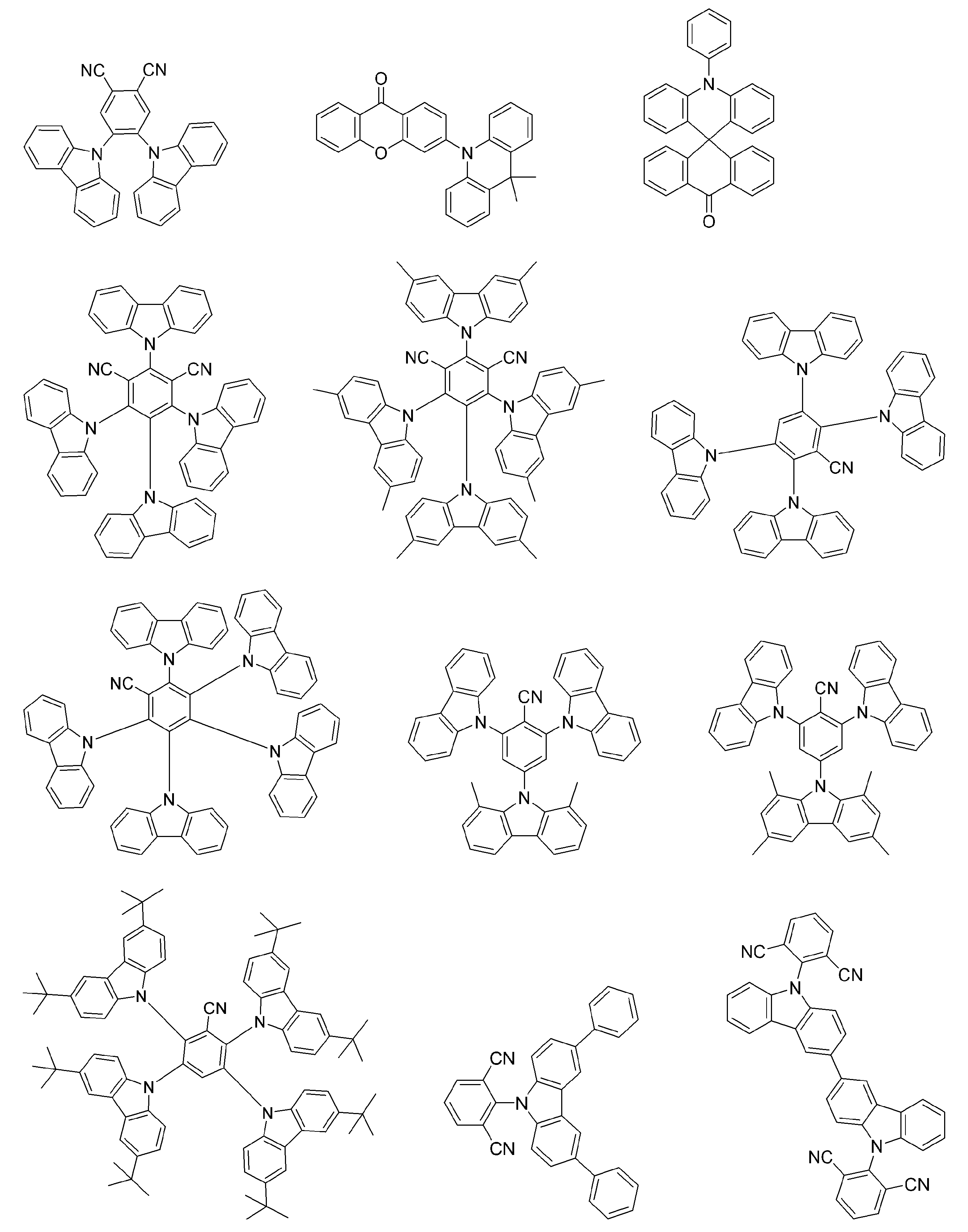

まず一般式(A)で表される化合物について説明する。

First, the compound represented by formula (A) will be described.
ここでいう置換アミノ基は、ジアリールアミノ基であることが好ましく、ジアリールアミノ基を構成する2つのアリール基は互いに連結して例えばカルバゾリル基となっていてもよい。また、置換アミノ基はR1~R5のいずれであってもよいが、例えばR1、R3、R4の組み合わせ、R2、R4の組み合わせなどを好ましく例示することができる。
一般式(A)に包含される化合物群と化合物の具体例については、本明細書の一部としてここに引用するWO2015/080183号公報およびWO2015/129715号公報を参照することができる。 In formula (A), one 0-4 of
The substituted amino group here is preferably a diarylamino group, and the two aryl groups constituting the diarylamino group may be linked to each other to form, for example, a carbazolyl group. Further, the substituted amino group may be any of R 1 to R 5 , and for example, a combination of R 1 , R 3 , R 4, a combination of R 2 , R 4 and the like can be preferably exemplified.
Reference can be made to WO2015 / 080183 and WO2015 / 129715 cited herein as part of this specification for specific examples of compounds and compounds included in general formula (A).
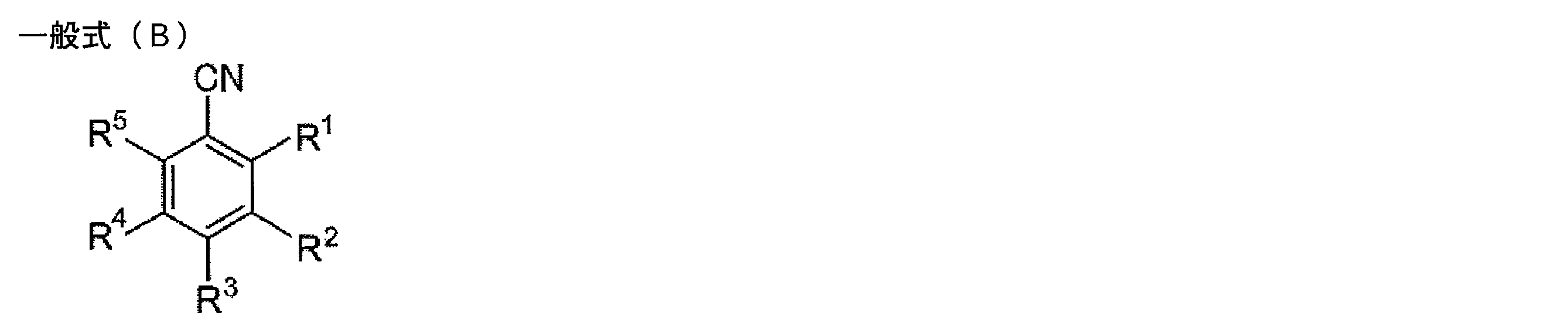


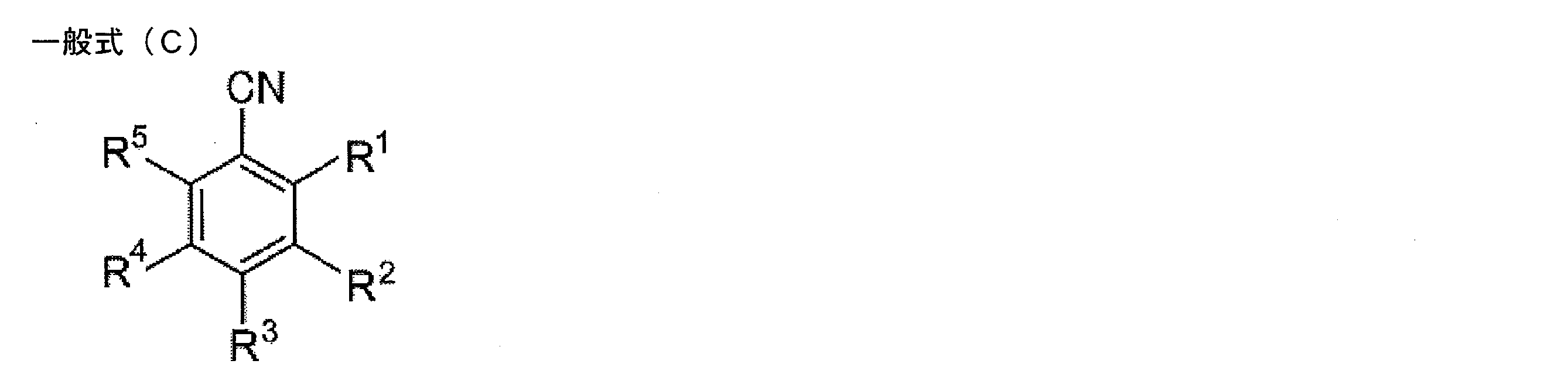

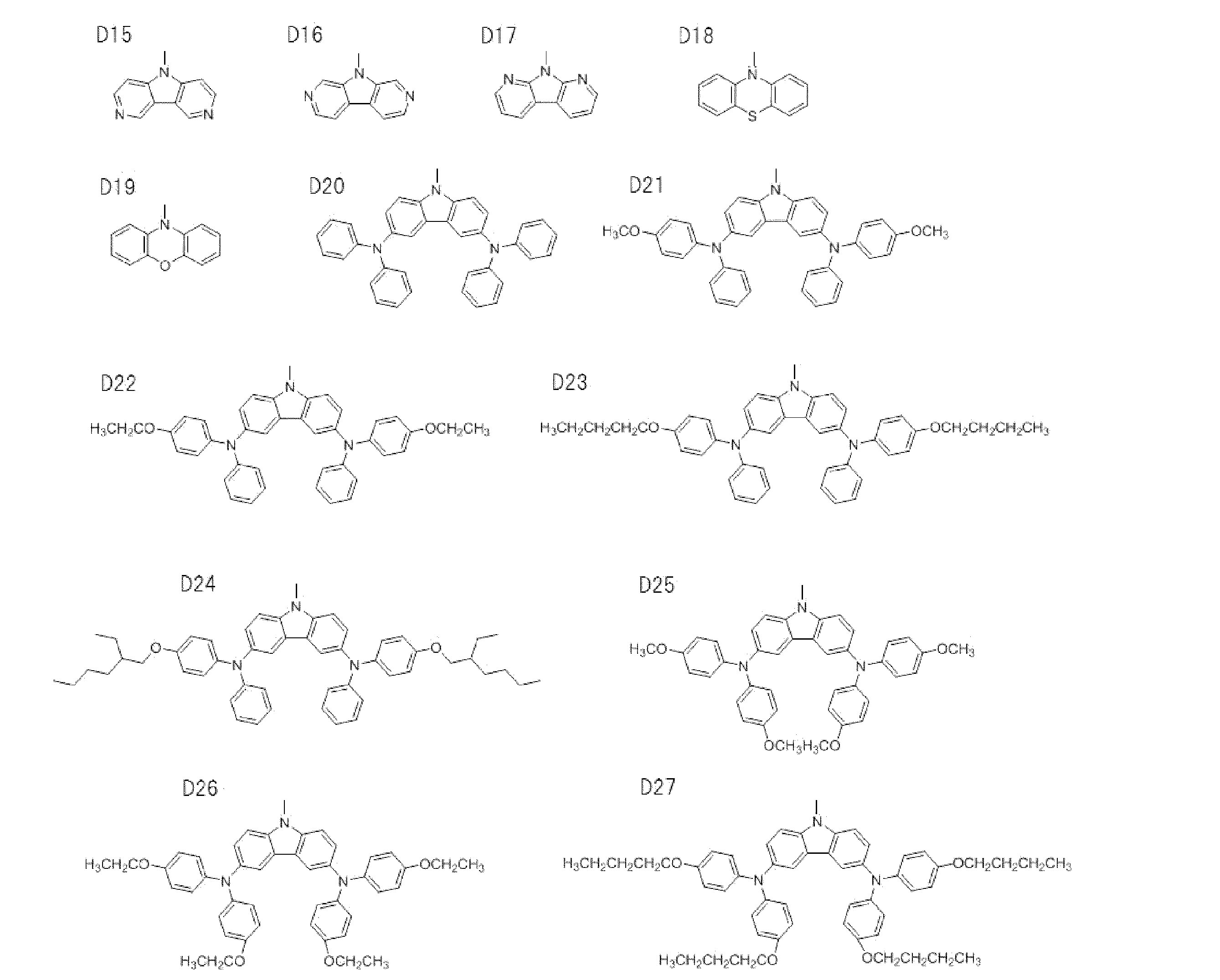

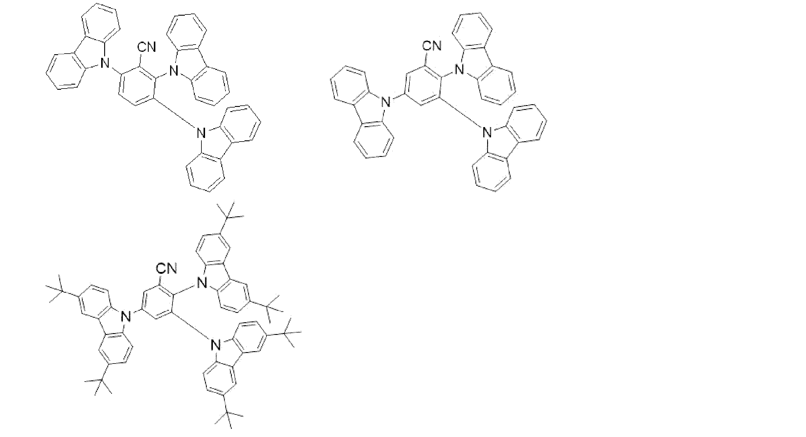

Spはベンゼン環またはビフェニル環を表し、
Czは1位と8位の少なくとも一方に置換基を有する9-カルバゾリル基(ここにおいて、9-カルバゾリル基のカルバゾール環の環骨格を構成する1~8位の炭素原子の少なくとも1つは窒素原子で置換されていてもよいが、1位と8位がともに窒素原子で置換されていることはない。)を表し、
Dはハメットのσp値が負である置換基を表し、
Aはハメットのσp値が正である置換基(ただし、シアノ基は除く)を表し、
aは1以上の整数を表し、mは0以上の整数を表し、nは1以上の整数を表すが、a+m+nはSpが表すベンゼン環またはビフェニル環に置換可能な最大置換基数を超えることはない。 In general formula (D),
Sp represents a benzene ring or a biphenyl ring,
Cz is a 9-carbazolyl group having a substituent in at least one of the 1-position and the 8-position (wherein at least one of the 1-8th carbon atoms constituting the ring skeleton of the carbazole ring of the 9-carbazolyl group is a nitrogen atom) But may not be substituted at the 1-position and 8-position with a nitrogen atom.)
D represents a substituent having a negative Hammett σ p value,
A represents a substituent having a positive Hammett σ p value (excluding a cyano group);
a represents an integer of 1 or more, m represents an integer of 0 or more, and n represents an integer of 1 or more, but a + m + n does not exceed the maximum number of substituents that can be substituted on the benzene ring or biphenyl ring represented by Sp. .
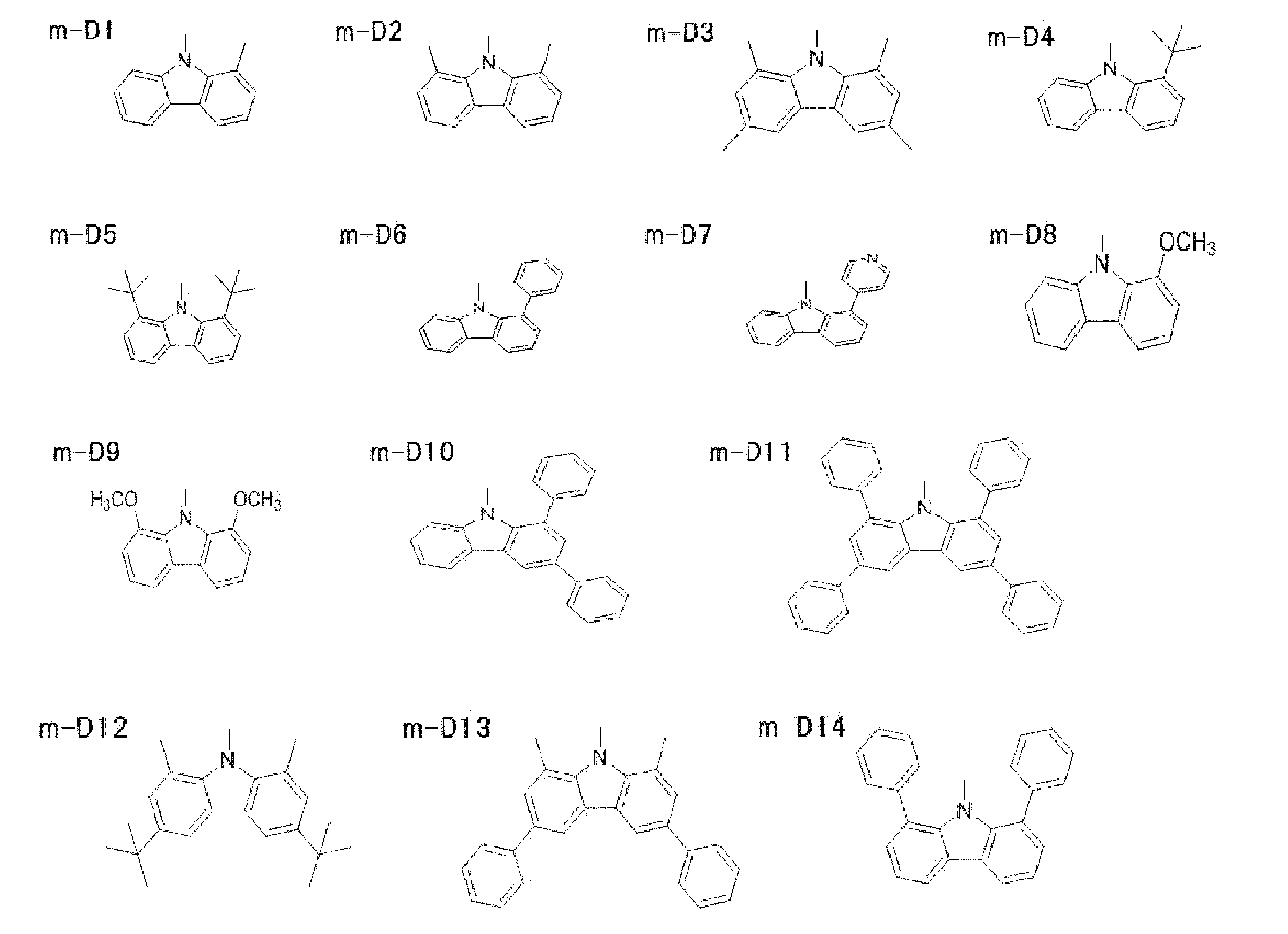

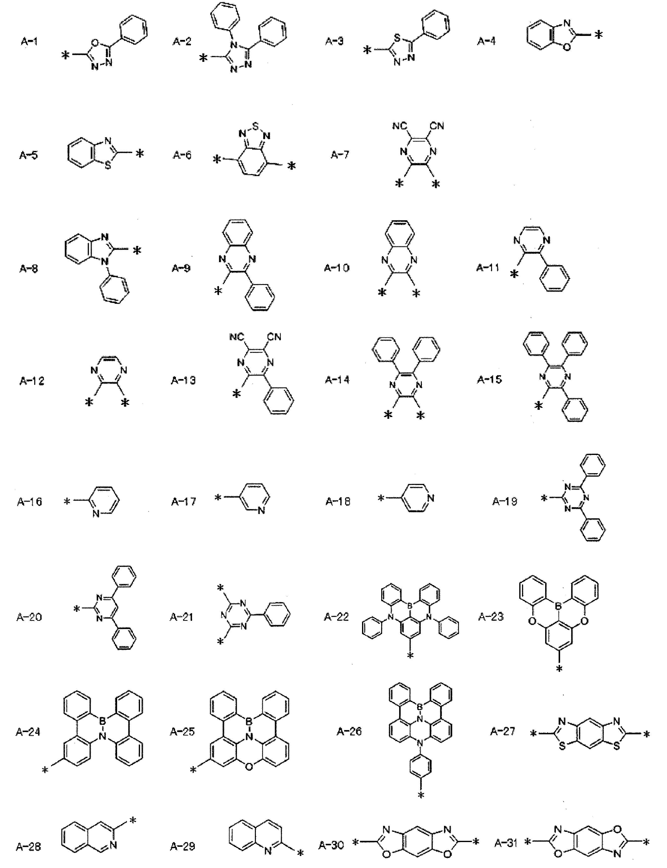
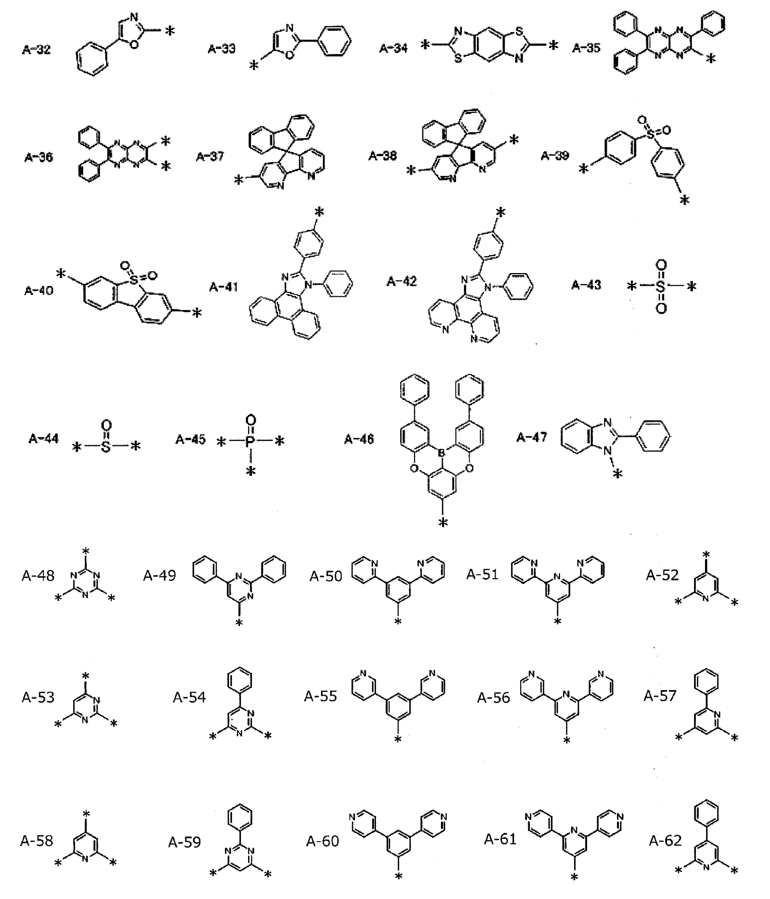


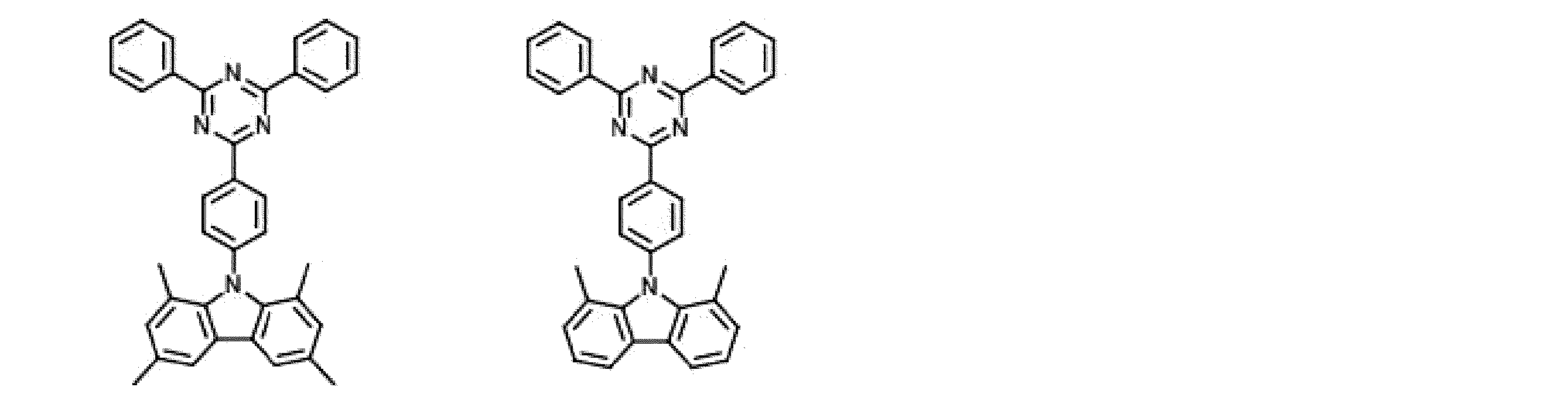

Arは、置換もしくは無置換のフェニレン基、置換もしくは無置換のビフェニルジイル基、または置換もしくは無置換のヘテロアリーレン基を表す。
R1~R10は、水素原子または置換基を表し、R1とR8の少なくとも一方は置換基である。また、R1~R8の少なくとも1つはジベンゾフリル基またはジベンゾチエニル基である。 In general formula (E),
Ar represents a substituted or unsubstituted phenylene group, a substituted or unsubstituted biphenyldiyl group, or a substituted or unsubstituted heteroarylene group.
R 1 to R 10 represent a hydrogen atom or a substituent, and at least one of R 1 and R 8 is a substituent. At least one of R 1 to R 8 is a dibenzofuryl group or a dibenzothienyl group.


以下において、一般式(F)で表される化合物の具体例を例示する。

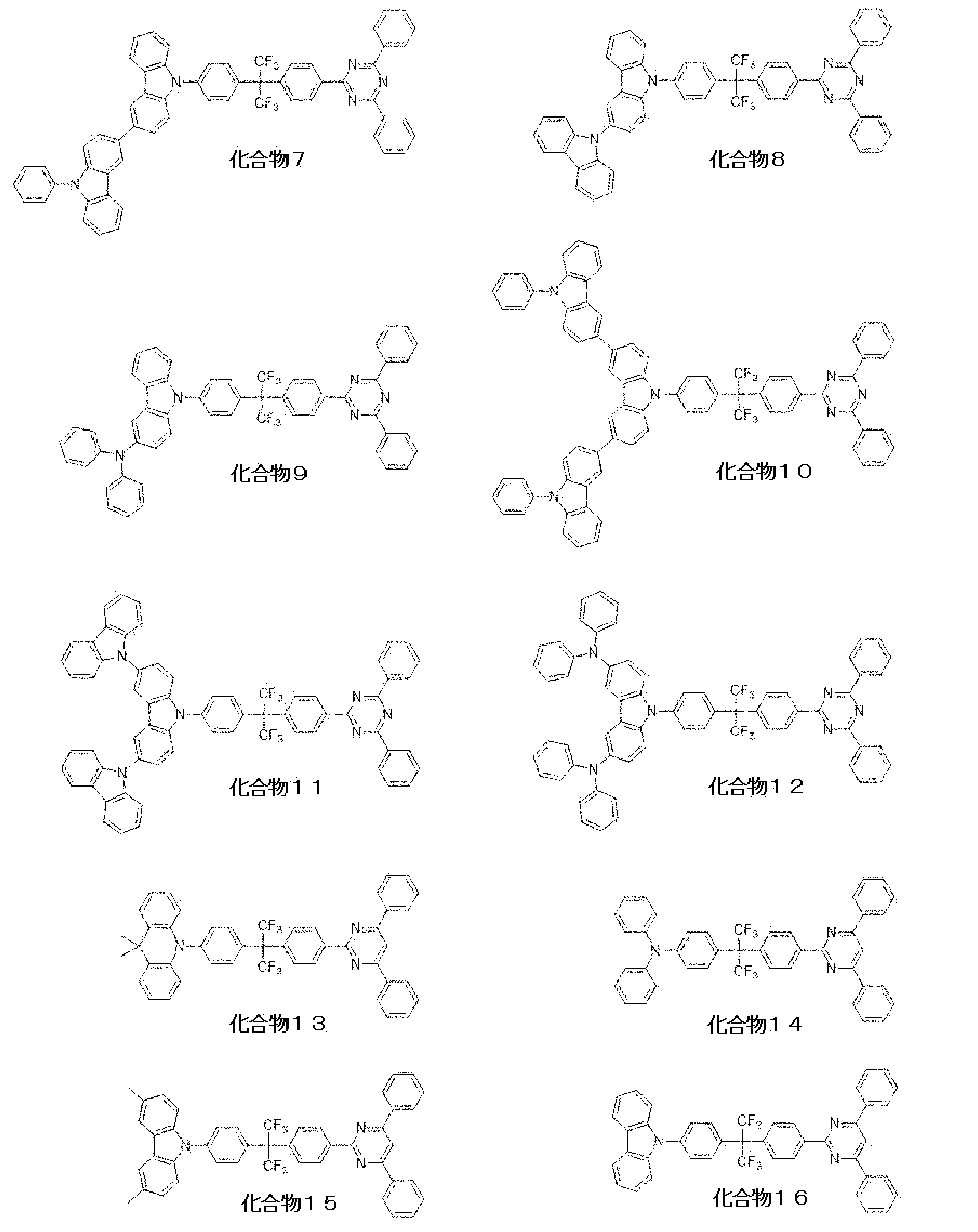


Below, the specific example of a compound represented by general formula (F) is illustrated.

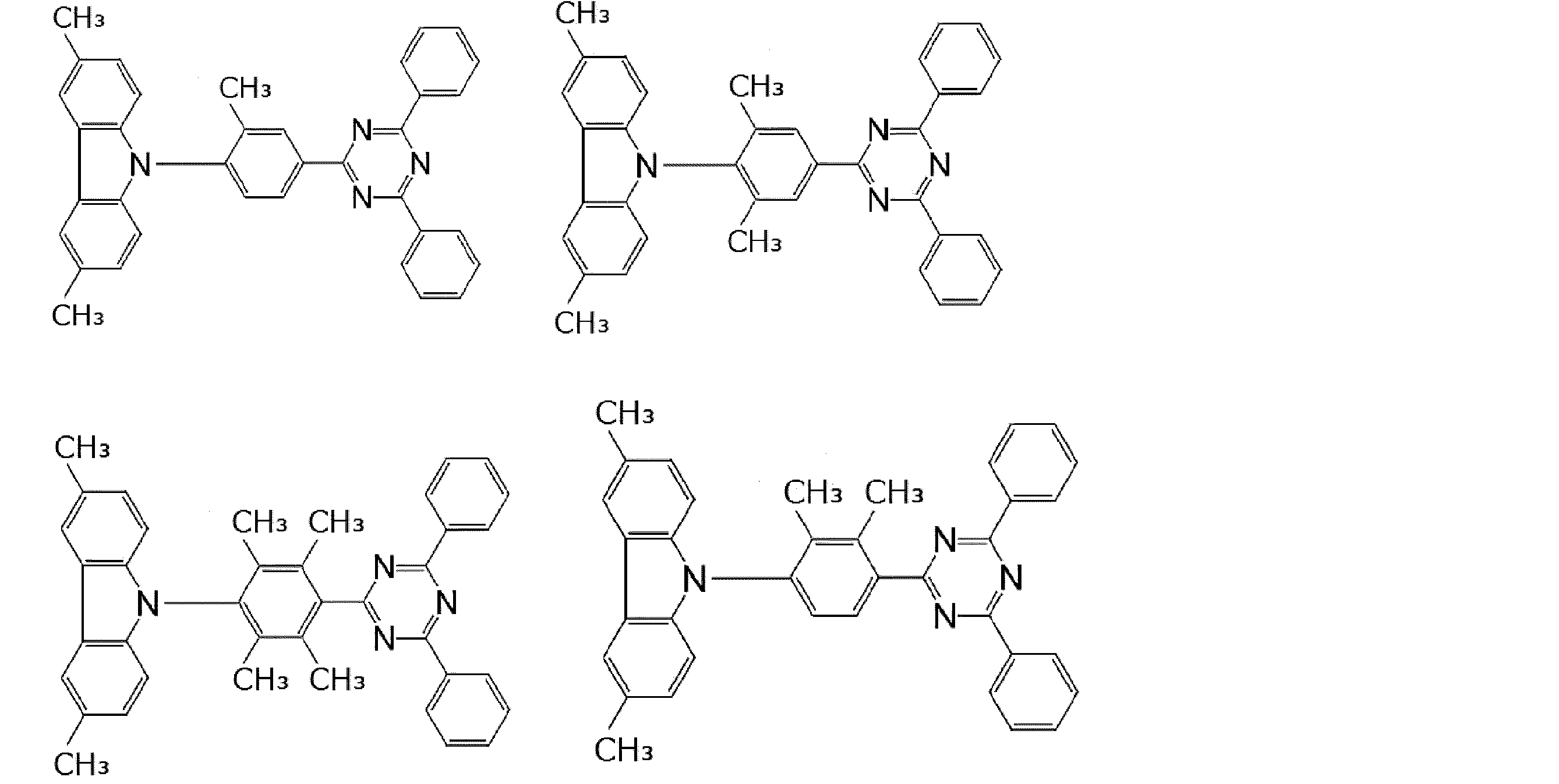
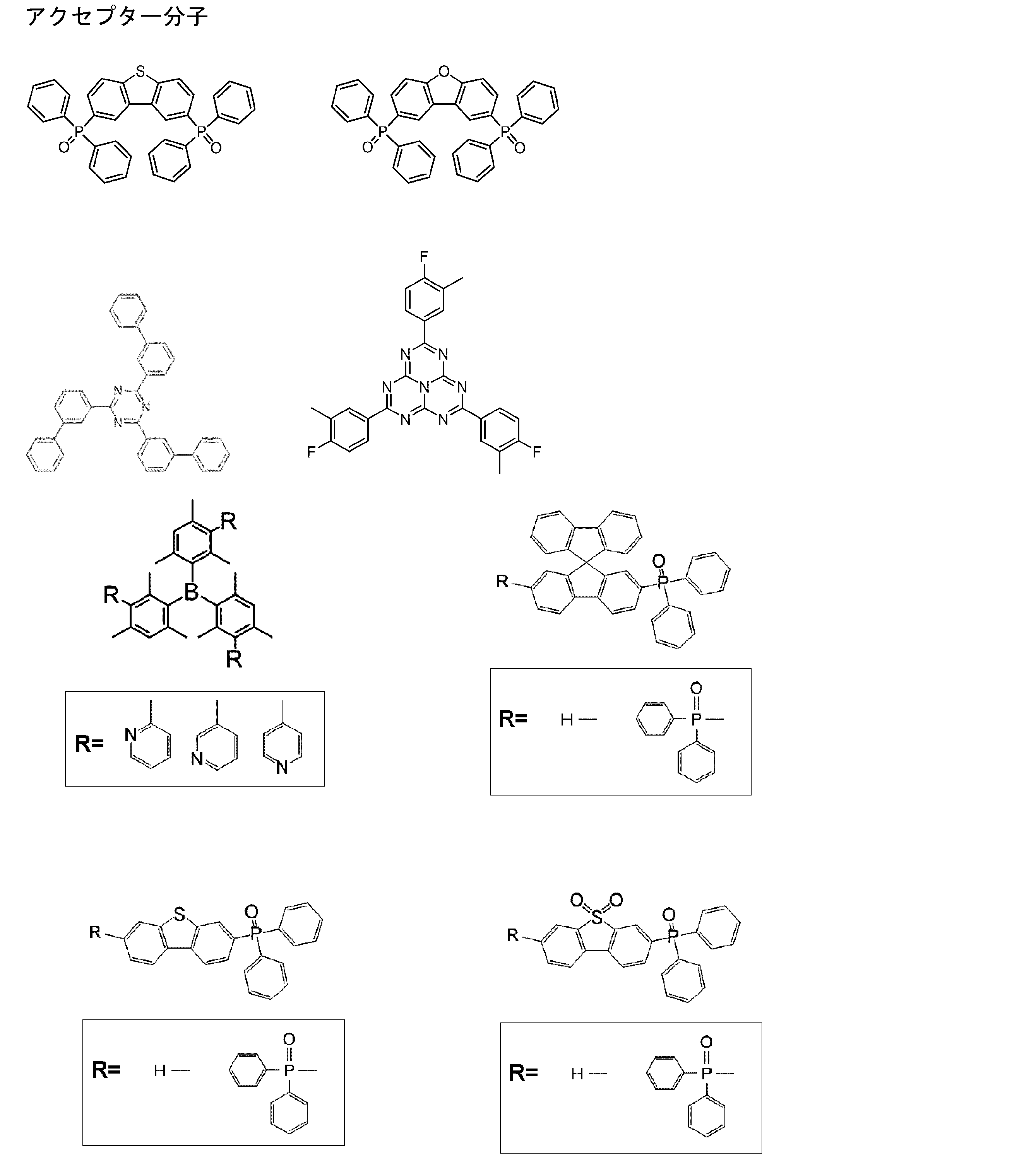


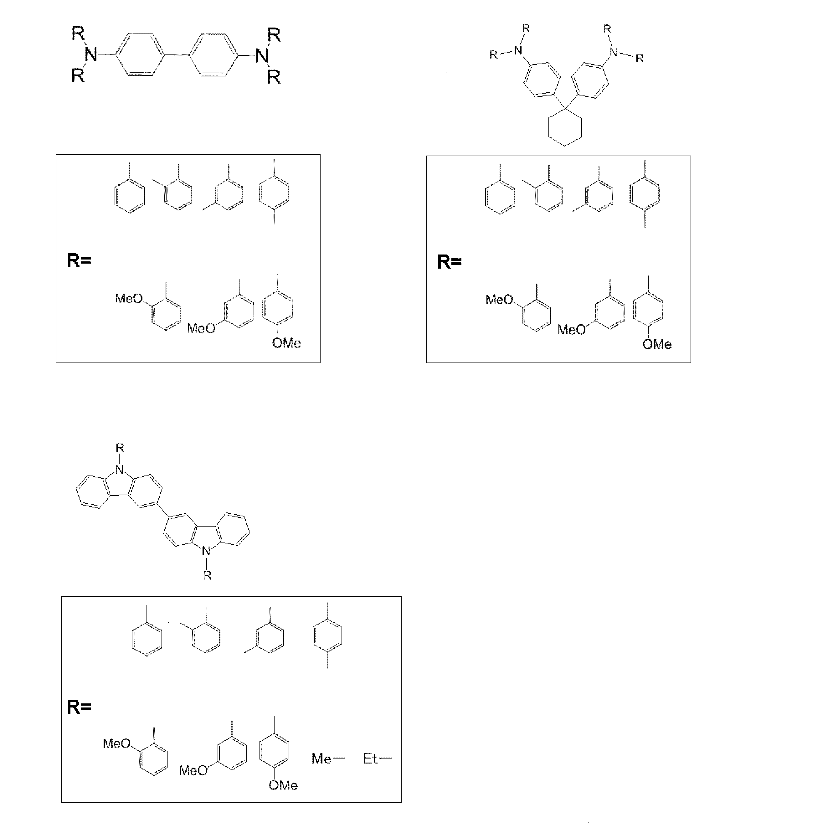
他の材料として、ホスト材料を挙げることができる。ホスト材料には、少なくとも最低励起三重項エネルギー準位ET1が式(1)を満たす化合物の最低励起三重項エネルギー準位ET1よりも高いものを用いることが好ましい。これにより、励起三重項状態にあるホスト材料のエネルギーを、式(1)を満たす化合物に円滑に移動させることができるとともに、式(1)を満たす化合物の励起三重項エネルギーを該化合物の分子内に閉じ込めることが可能になり、そのエネルギーを有機発光素子の発光に効果的に利用することができる。ホスト材料を用いる場合は、励起子生成層における式(1)を満たす化合物の含有量を50質量%以下とすることが好ましく、効率を考慮して25質量以下、15質量%以下、10%質量以下とすることもできる。 The exciton generation layer may be composed of a compound satisfying the formula (1) or a material composed only of an acceptor molecule and a donor molecule constituting an exciplex emitting delayed fluorescence, or may include other materials. . The lower limit value of the contents of the acceptor molecule and the donor molecule constituting the compound satisfying the formula (1) or the exciplex emitting delayed fluorescence in the exciton generation layer is, for example, more than 1 mass%, more than 5 mass%, more than 10 mass% It may be more than 20% by mass, more than 50% by mass, more than 75% by mass. Furthermore, the concentration may not be fixed but may have a concentration gradient in the thickness direction of the light emitting layer.
Examples of other materials include host materials. It is preferable to use a host material having at least the lowest excited triplet energy level E T1 higher than the lowest excited triplet energy level E T1 of the compound satisfying the formula (1). Thereby, the energy of the host material in the excited triplet state can be smoothly transferred to the compound satisfying the formula (1), and the excited triplet energy of the compound satisfying the formula (1) can be transferred into the molecule of the compound. The energy can be effectively utilized for light emission of the organic light emitting device. When the host material is used, the content of the compound satisfying the formula (1) in the exciton generation layer is preferably 50% by mass or less, and 25% or less, 15% by mass or less, 10% by mass in consideration of efficiency. It can also be as follows.
また、その他の態様として、励起子生成層は、式(1)を満たす化合物または遅延蛍光を発するエキサイプレックスを構成するアクセプター分子とドナー分子が高分子材料(結着用樹脂)や無機材料中に分散されて構成されたものであってもよい。 The exciton generation layer may further contain a dopant in addition to the host material, the compound satisfying the formula (1), or the acceptor molecule and the donor molecule constituting the exciplex emitting delayed fluorescence. The content of the dopant in the exciton generation layer is preferably less than the content of the acceptor molecule and the donor molecule constituting the compound satisfying the formula (1) or the exciplex emitting delayed fluorescence, for example, 10% by mass or less, 5 It can be used at mass% or less, 3 mass% or less, 1 mass% or less, 0.5 mass% or less, and 0.001 mass% or more, 0.01 mass% or more, 0.1 mass% or more. It is possible to use. As a dopant, it is possible to employ | adopt the same thing as the luminescent material used for a light emitting layer, for example. By adopting the same light emitting material as the light emitting layer as the dopant of the exciton generation layer, energy is transferred from the compound satisfying the formula (1) to the dopant in the exciton generation layer and the light emitting material in the light emission layer. Emits light. As a result, the energy of the compound satisfying the formula (1) can be used for light emission more efficiently. Note that the exciton generation layer containing such a dopant also functions as a light emitting layer because the dopant emits light.
As another embodiment, the exciton generation layer includes a compound satisfying the formula (1) or an acceptor molecule and a donor molecule constituting an exciplex emitting delayed fluorescence dispersed in a polymer material (binding resin) or an inorganic material. And may be configured.
発光層は発光材料を含む。発光層が含む発光材料は、1種類単独であってもよいし、2種類以上の組み合わせであってもよい。また、2種類以上の発光材料を用いる場合、各発光材料の発光色は同じ色相であってもよいし、異なる色相であってもよい。異なる色相の発光材料を用いることにより、その混合色や白色の発光を得ることができる。
発光層に用いる発光材料の種類は特に制限されず、蛍光発光材料、遅延蛍光材料、燐光発光材料のいずれであってもよいが、蛍光発光材料または遅延蛍光発光材料であることがより好ましい、蛍光発光材料であることがより好ましい。また、発光材料には、最低励起一重項エネルギー準位ES1と最低励起三重項エネルギー準位ET1の差ΔESTが式(1)を満たす化合物よりも大きい化合物を用いることが好ましく、ΔEST > 0.3eVである化合物を用いることがより好ましく、例えばΔEST > 0.5eVである化合物を用いることもできる。
また、発光材料は、励起子生成層が含む式(1)を満たす化合物よりも、その最低励起一重項エネルギー準位ES1が低いことが好ましい。これにより、励起子生成層において励起一重項状態に遷移した式(1)を満たす化合物のエネルギーを、発光層の発光材料に円滑に移動させることができ、そのエネルギーを発光材料の発光に効果的に利用することができる。発光材料の最低励起一重項エネルギー準位ES1が、励起子生成層が含む式(1)を満たす化合物よりも高い場合は、両者の最低励起一重項エネルギー準位ES1の差は0.5eV以下であることが好ましく、0.3eV以下であることがより好ましく、0.2eV以下であることがさらに好ましい。
発光材料が発光する光の種類は、特に限定はされないが、可視光、赤外光、紫外光であることが好ましく、可視光であることがより好ましい。
以下に、発光材料として用いることができる好ましい化合物を発光色毎に具体的に例示する。ただし、本発明において用いることができる発光材料は、以下の例示化合物によって限定的に解釈されることはない。なお、以下の例示化合物の構造式において、Etはエチル基を表し、i-Prはイソプロピル基を表す。 [Light emitting layer]
The light emitting layer includes a light emitting material. The light emitting material included in the light emitting layer may be a single type or a combination of two or more types. When two or more kinds of light emitting materials are used, the light emission colors of the light emitting materials may be the same hue or different hues. By using light emitting materials having different hues, it is possible to obtain a mixed color or white light emission.
The type of the light emitting material used for the light emitting layer is not particularly limited, and may be any of a fluorescent light emitting material, a delayed fluorescent material, and a phosphorescent light emitting material, but is more preferably a fluorescent light emitting material or a delayed fluorescent light emitting material. More preferably, it is a luminescent material. In addition, it is preferable to use a compound whose difference ΔE ST between the lowest excited singlet energy level E S1 and the lowest excited triplet energy level E T1 is larger than the compound satisfying the formula (1) as the light emitting material, and ΔE ST More preferably, a compound with> 0.3 eV is used, for example, a compound with ΔE ST > 0.5 eV can be used.
In addition, the light emitting material preferably has a lower lowest excited singlet energy level E S1 than a compound satisfying the formula (1) included in the exciton generation layer. Thereby, the energy of the compound satisfying the formula (1) that has transitioned to the excited singlet state in the exciton generation layer can be smoothly transferred to the light emitting material of the light emitting layer, and this energy is effective for light emission of the light emitting material. Can be used. When the lowest excited singlet energy level E S1 of the light emitting material is higher than the compound satisfying the formula (1) included in the exciton generation layer, the difference between the lowest excited singlet energy levels E S1 is 0.5 eV. Or less, more preferably 0.3 eV or less, and even more preferably 0.2 eV or less.
The type of light emitted from the light emitting material is not particularly limited, but is preferably visible light, infrared light, or ultraviolet light, and more preferably visible light.
Below, the preferable compound which can be used as a luminescent material is specifically illustrated for every luminescent color. However, the light-emitting material that can be used in the present invention is not limitedly interpreted by the following exemplary compounds. In the structural formulas of the following exemplary compounds, Et represents an ethyl group, and i-Pr represents an isopropyl group.


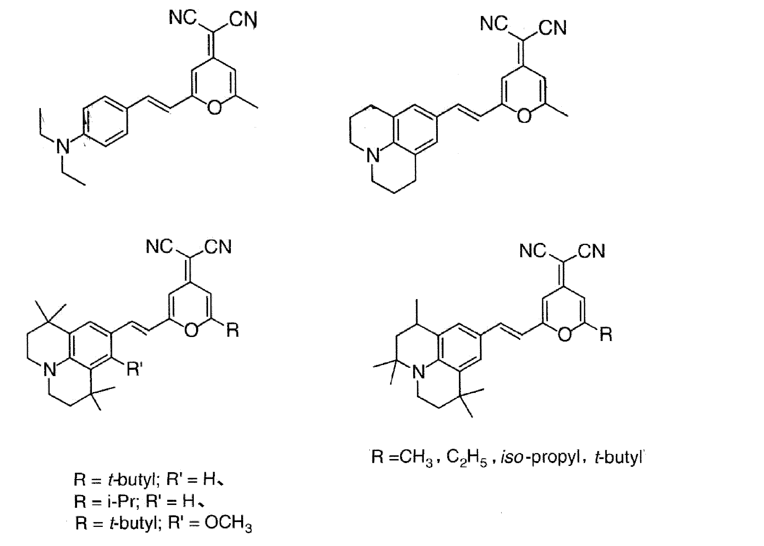

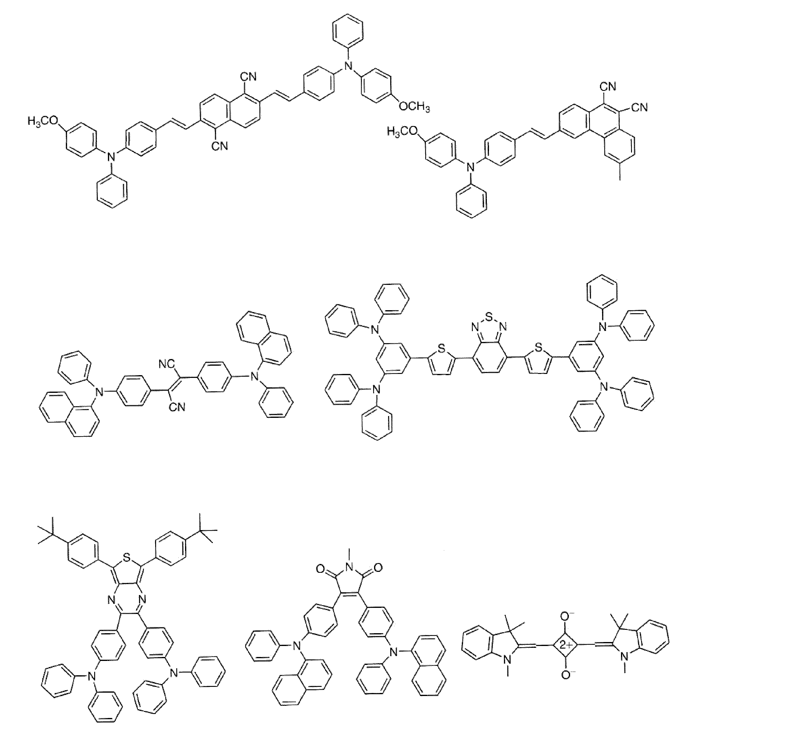


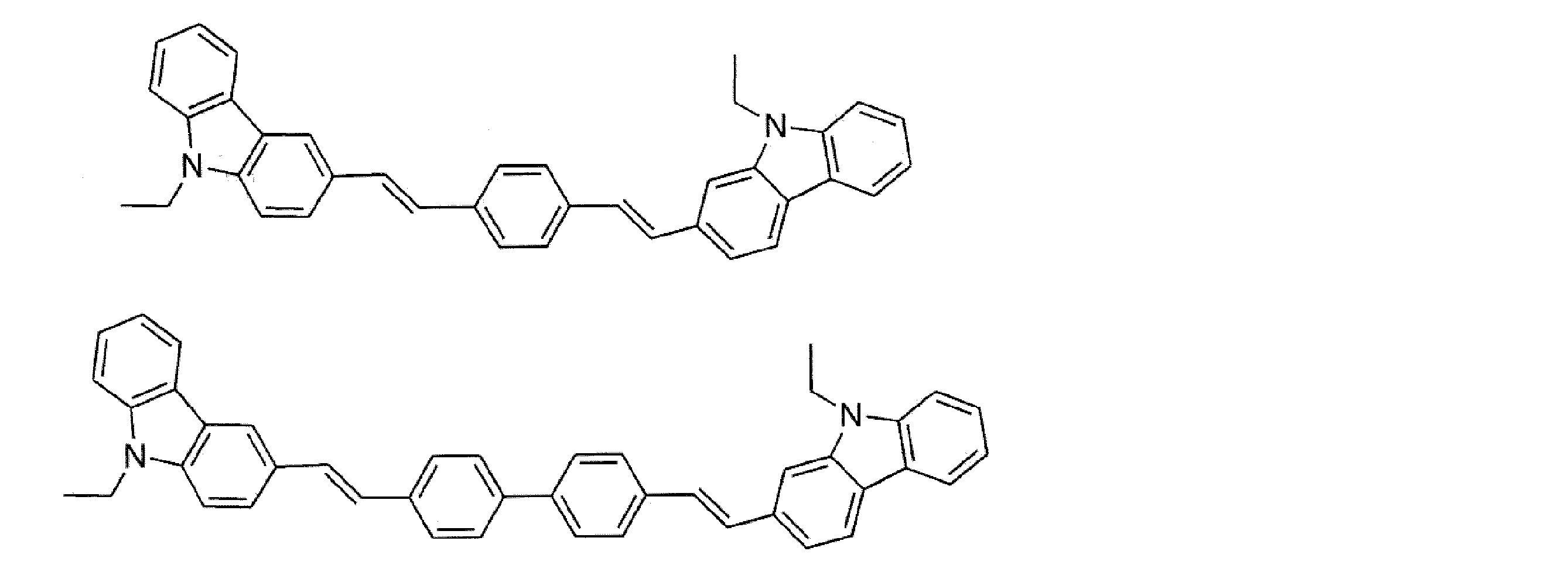

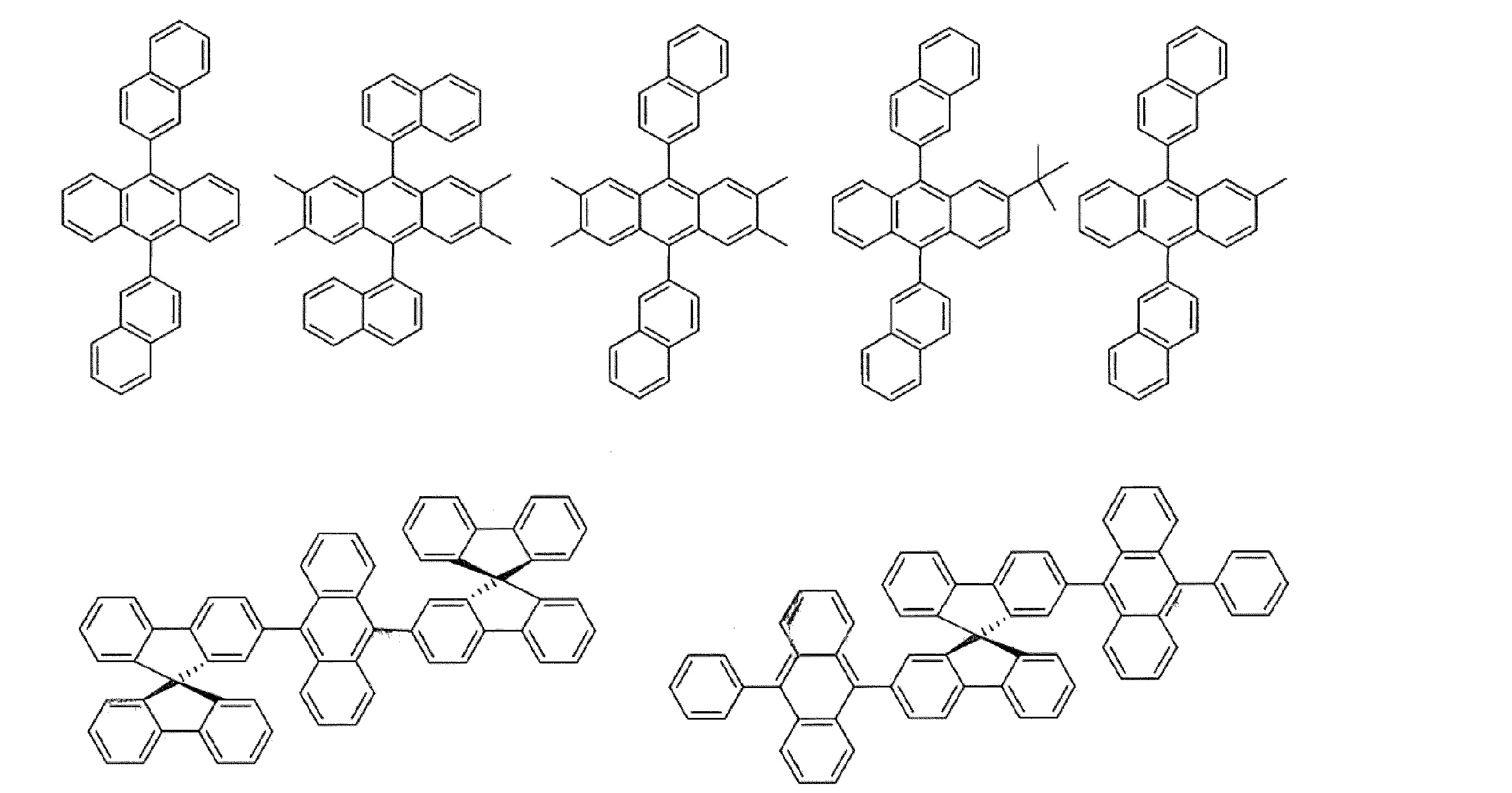


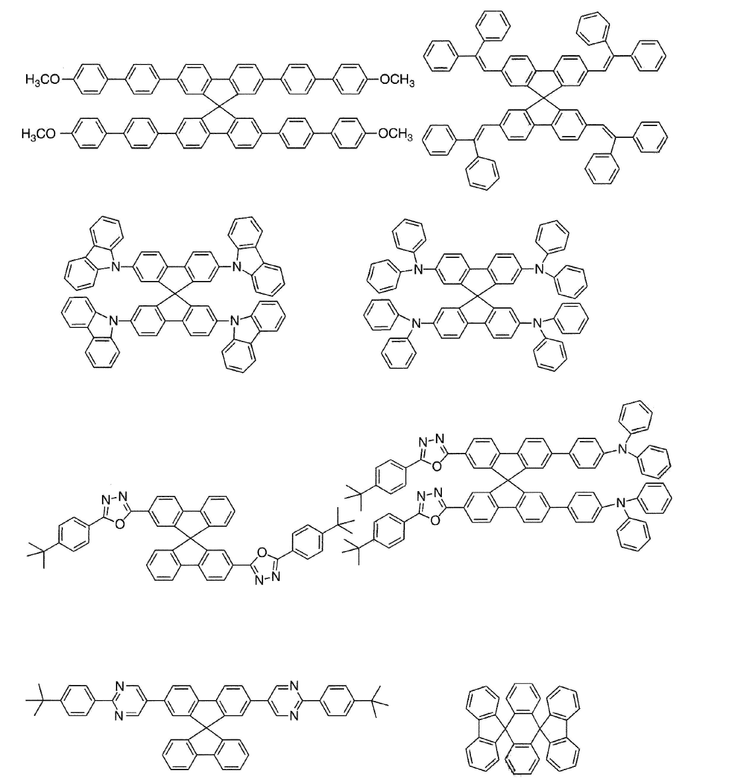


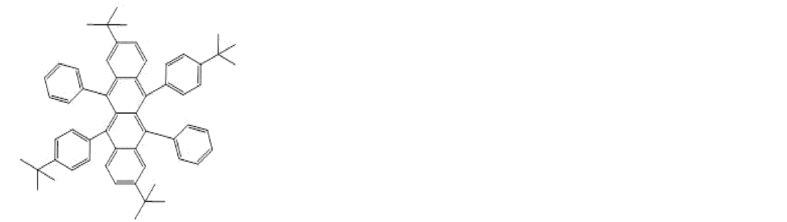

量子ドットの構成材料種は特に制限されない。通常は、周期表第14~16族から選択される1以上の元素により構成された量子ドットを好ましく用いることができる。例えば、C、Si、Ge、Sn、P、Se、Teなどの単一元素からなる単体であってもよいし、2つ以上の元素からなる化合物であってもよい。2つ以上の元素からなる量子ドットとしては、SiC、SnO2、Sn(II)Sn(IV)S3、SnS2、SnS、SnSe、SnTe、PbS、PbSe、PbTe、BN、BP、BAs、AlN、AlP、AlAs、AlSb、GaN、GaP、GaAs、GaSb、InN、InP、InAs、InSb、Al2S3、Al2Se3、Ga2S3、Ga2Se3、Ga2Te3、In2O3、In2S3、In2Se3、In2Te3、TlCl、TlBr、TlI、ZnO、ZnS、ZnSe、ZnTe、CdO、CdS)、CdSe、CdTe、HgS、HgSe、HgTe、As2S3、As2Se3、As2Te3、Sb2S3、Sb2Se3、Sb2Te3、Bi2S3、Bi2Se3、Bi2Te3、Cu2O、Cu2Se、CuCl、CuBr、CuI、AgCl、AgBr、NiO、CoO、CoS、Fe3O4、FeS、MnO、MoS2、WO2、VO、VO2、Ta2O5、TiO2、Ti2O5、Ti2O3、Ti5O9、MgS、MgSe、CdCr2O4、CdCr2Se4、CuCr2S4、HgCr2Se4、BaTiO3を挙げることができる。また、これらを混合して用いることもできる。上記の例示の中では、CdSe、ZnSe、CdS、CdSeS/ZnSを好ましく採用することができる。また、本発明では、市販の量子ドットを用いることもできる。例えば、Aldorich社製の型番753785や753742などを好ましく用いることができる。
本発明で用いる量子ドットは、表面がコーティングされているものであってもよい。
量子ドットは、適切な溶剤を用いてスピンコートする等の方法により製膜することができる。溶剤としては、例えばトルエン、ヘキサン、ハロゲン溶媒、アルコール系溶媒、水などを用いることができる。 Quantum dots can also be used for the light emitting layer. Quantum dots are nano-sized semiconductor particles having a quantum confinement effect. The band gap value of the quantum dot can be controlled by adjusting the constituent material type and particle diameter of the quantum dot. For this reason, there is an advantage that it is easy to prepare quantum dots that emit light in a desired wavelength region. As a result, the target emission chromaticity can be realized without using a color filter, so that high efficiency can be realized. The diameter of the quantum dots that can be used in the present invention is preferably 2 to 10 nm, more preferably 4 to 8 nm, and even more preferably 5 to 6 nm.
The constituent material type of the quantum dot is not particularly limited. Usually, a quantum dot composed of one or more elements selected from Groups 14 to 16 of the periodic table can be preferably used. For example, it may be a simple substance composed of a single element such as C, Si, Ge, Sn, P, Se, or Te, or may be a compound composed of two or more elements. The quantum dots composed of two or more elements, SiC, SnO 2, Sn ( II) Sn (IV)
The quantum dot used in the present invention may have a surface coated.
The quantum dots can be formed by a method such as spin coating using an appropriate solvent. As the solvent, for example, toluene, hexane, a halogen solvent, an alcohol solvent, water, or the like can be used.
なお、各層に含まれるキャリア輸送性化合物は、1種類であってもよいし、2種類以上であってもよい。2種類以上の化合物が含まれている場合は、その存在比は各層で異なっていてもよい。 Examples of the carrier transporting compound herein include compounds used in the host materials described in the “exciton generation layer” and “light emitting layer” columns. The exciton generation layer and the light emitting layer may be composed of only a carrier transporting compound other than the compound satisfying the formula (1), the compound emitting delayed fluorescence, and the light emitting material, or only a part of the compound may be carrier transportable. Although it may be composed of a compound, it is preferably composed only of a carrier transporting compound. Also, the isolation layer may be composed only of the carrier transporting compound, or only part of it may be composed of the carrier transporting compound, but it is composed only of the carrier transporting compound. Is preferred.
The carrier transporting compound contained in each layer may be one type or two or more types. When two or more kinds of compounds are contained, the abundance ratio may be different in each layer.
発光は、蛍光発光であり、遅延蛍光発光や燐光発光を含んでいてもよい。遅延蛍光は、エネルギー供与により励起状態になった化合物において、励起三重項状態から励起一重項状態への逆項間交差が生じた後、その励起一重項状態から基底状態に戻る際に放射される蛍光であり、直接生じた励起一重項状態からの蛍光(通常の蛍光)よりも遅れて観測される蛍光である。 In the organic light emitting device of the present invention, light emission is caused at least from a light emitting material included in the light emitting layer. However, part of the light emission may be light emission from a compound satisfying the formula (1) included in the exciton generation layer, an exciplex emitting delayed fluorescence, or a host material included in the exciton generation layer or the isolation layer. In the present invention, it is preferable that 25% or more of the emitted light is emitted from the light emitting material, 50% or more of the emitted light is preferably emitted from the light emitting material, and 80% or more of the emitted light is emitted from the light emitting material. More preferably, 90% or more of the emitted light is more preferably emitted from the light emitting material, and more preferably 99% or more of the emitted light is emitted from the light emitting material.
The light emission is fluorescence emission, and may include delayed fluorescence emission or phosphorescence emission. Delayed fluorescence is emitted when a compound that has been excited by energy donation returns from the excited singlet state to the ground state after a reverse intersystem crossing from the excited triplet state to the excited singlet state occurs. This is fluorescence, which is observed after the fluorescence from the directly excited singlet state (normal fluorescence).
本発明の有機発光素子は、さらに、励起子生成層と発光層の間に隔離層が存在していてもよい。隔離層を存在させることによって、励起子生成層に含まれる式(1)を満たす化合物または遅延蛍光を発するエキサイプレックスと、発光層に含まれる発光材料との距離がより長くなるため、励起子生成層において励起三重項状態に遷移した式(1)を満たす化合物または遅延蛍光を発するエキサイプレックスのエネルギーが発光層に含まれる発光材料へデクスター機構で移動することをより確実に抑制することができる。その結果、式(1)を満たす化合物または遅延蛍光を発するエキサイプレックスが励起三重項状態から励起一重項状態に逆項間交差する確率が高くなると推測され、励起三重項状態に遷移した式(1)を満たす化合物または遅延蛍光を発するエキサイプレックスのエネルギーを蛍光発光に有効に利用することができる。
発光層の陽極側と陰極側のそれぞれに励起子生成層が存在している場合は、いずれか一方の励起子生成層と発光層の間にだけ隔離層が存在していてもよいし、両方の励起子生成層と発光層の間にそれぞれ隔離層が存在していてもよい。好ましいのは、両方にそれぞれ隔離層が存在している態様である。 [Isolation layer]
In the organic light emitting device of the present invention, an isolation layer may further exist between the exciton generation layer and the light emitting layer. By the presence of the isolation layer, the distance between the compound satisfying the formula (1) contained in the exciton generation layer or the exciplex emitting delayed fluorescence and the light emitting material contained in the light emitting layer becomes longer, so that exciton generation occurs. It is possible to more reliably suppress the energy of the exciplex that emits delayed fluorescence or the compound that satisfies Formula (1) that has transitioned to the excited triplet state in the layer from moving to the light-emitting material contained in the light-emitting layer. As a result, it is presumed that the compound satisfying the formula (1) or the exciplex emitting delayed fluorescence has a high probability of crossing from the excited triplet state to the excited singlet state, and the transition to the excited triplet state (1 Or the energy of an exciplex that emits delayed fluorescence can be effectively used for fluorescence emission.
When an exciton generation layer exists on each of the anode side and the cathode side of the light emitting layer, an isolation layer may exist only between either one of the exciton generation layer and the light emitting layer, or both An isolation layer may exist between each of the exciton generation layer and the light emitting layer. Preferred is an embodiment in which an isolation layer is present on both.
複数の隔離層が存在する場合、各隔離層の材料は、同一であっても異なっていてもよいが、各隔離層がキャリア輸送性化合物を含むことが好ましい。複数の隔離層は、キャリア輸送性化合物により全体が構成されていてもよいし、キャリア輸送性化合物により一部が構成されていてもよいが、キャリア輸送性化合物により全体が構成されていることが好ましい。また、複数の隔離層にキャリア輸送性化合物は、1種類であってもよいし、2種類以上であってもよい。
また、少なくとも1層の隔離層と、上記の発光層は、発光層が含む発光材料とは異なるキャリア輸送性化合物を含むことが好ましい。発光材料とは異なるキャリア輸送性化合物として、「発光層」の欄で説明したホスト材料に用いられる化合物を挙げることができる。隔離層は、発光層に含まれているのと同じキャリア輸送性化合物により全体が構成されていてもよいし、発光層に含まれているのと同じキャリア輸送性化合物により一部が構成されていてもよいが、発光層とキャリア輸送性化合物により全体が構成されていることが好ましい。発光層は、発光材料を除く材料の全体が少なくとも1層の隔離層に含まれているのと同じキャリア輸送性化合物により構成されていてもよいし、その一部が隔離層に含まれているのと同じキャリア輸送性化合物により構成されていてもよいが、発光材料を除く材料の全体が隔離層と同じキャリア輸送性化合物により構成されていることが好ましい。発光層と隔離層の化合物は、1種類であってもよいし、2種類以上であってもよい。 The material of the isolation layer may be any of an inorganic material, an organic material, and an organic-inorganic hybrid material having an inorganic part and an organic part, but preferably contains an organic compound, and more preferably consists only of an organic compound.
When a plurality of isolation layers are present, the material of each isolation layer may be the same or different, but each isolation layer preferably contains a carrier transporting compound. The plurality of isolation layers may be entirely constituted by the carrier transporting compound, or may be partially constituted by the carrier transporting compound, but may be entirely constituted by the carrier transporting compound. preferable. In addition, the number of carrier transporting compounds in the plurality of isolation layers may be one, or two or more.
Moreover, it is preferable that at least 1 isolation layer and said light emitting layer contain the carrier transportable compound different from the light emitting material which a light emitting layer contains. Examples of the carrier transporting compound different from the light emitting material include the compounds used in the host material described in the “Light emitting layer” column. The isolation layer may be entirely constituted by the same carrier transporting compound contained in the light emitting layer, or partly constituted by the same carrier transporting compound contained in the light emitting layer. However, it is preferable that the whole is constituted by the light emitting layer and the carrier transporting compound. The light emitting layer may be composed of the same carrier transporting compound as the whole of the material excluding the light emitting material is included in at least one isolation layer, and a part thereof is included in the isolation layer. However, it is preferable that the entire material excluding the light emitting material is composed of the same carrier transporting compound as that of the isolation layer. There may be one type of compound of a light emitting layer and an isolation layer, and two or more types may be sufficient as it.
本発明の有機発光素子が有機エレクトロルミネッセンス素子である場合、さらに、発光層と励起子生成層のうち最も陽極側に存在する層に直接接するように層が形成されていてもよいし、また、発光層と励起子生成層のうち最も陰極側に存在する層に直接接するように層が形成されていてもよく、これら両方に層が形成されていてもよい。これらの直接接するように形成される層を便宜的に外側層と呼ぶ。本発明の有機発光素子は、「外側層/発光層/(隔離層)/励起子生成層」、「外側層/励起子生成層/発光層」、「発光層/(隔離層)/励起子生成層/外側層」、「励起子生成層/(隔離層)/発光層/外側層」の構造を含むものとすることが可能である。 [Other layers]
When the organic light-emitting device of the present invention is an organic electroluminescence device, the layer may be further formed so as to be in direct contact with the layer present on the most anode side of the light-emitting layer and the exciton generation layer, Of the light emitting layer and the exciton generation layer, the layer may be formed so as to be in direct contact with the layer present on the most cathode side, or the layer may be formed on both of them. These layers formed so as to be in direct contact with each other are referred to as outer layers for convenience. The organic light-emitting device of the present invention includes “outer layer / luminescent layer / (isolating layer) / exciton generating layer”, “outer layer / exciton generating layer / luminescent layer”, “luminescent layer / (isolating layer) / exciton”. It is possible to include a structure of “generation layer / outer layer” and “exciton generation layer / (isolation layer) / light emitting layer / outer layer”.
陽極側と陰極側の両方に外側層を有する場合、これらの外側層の材料は、同一であっても異なっていてもよい。外側層は、キャリア輸送性化合物を含むことが好ましい。また、発光層と励起子生成層(と隔離層)がキャリア輸送性化合物を含む場合、外側層も、その化合物を含むことが好ましい。化合物としては、「励起子生成層」、「発光層」の欄で説明したホスト材料を挙げることができる。外側層は、励起子生成層と発光層(と隔離層)とキャリア輸送性化合物により全体が構成されていてもよいし、その一部がキャリア輸送性化合物により構成されていてもよいが、キャリア輸送性化合物により全体が構成されていることが好ましい。また、外側層が含むキャリア輸送性化合物は、1種類であってもよいし、2種類以上であってもよい。
以上の励起子生成層、発光層、隔離層および外側層は、必要に応じて添加剤(ドナー、アクセプター等)等を含んでいてもよい。 The material of the outer layer may be any of an inorganic material, an organic material, and an organic-inorganic hybrid material having an inorganic part and an organic part, but preferably contains an organic-inorganic hybrid material or an organic compound. Further, it may be a co-evaporated film containing an organic compound.
In the case of having outer layers on both the anode side and the cathode side, the materials of these outer layers may be the same or different. The outer layer preferably contains a carrier transporting compound. Moreover, when a light emitting layer and an exciton production | generation layer (and isolation layer) contain a carrier transportable compound, it is preferable that an outer side layer also contains the compound. Examples of the compound include the host materials described in the columns of “exciton generation layer” and “light emitting layer”. The outer layer may be entirely constituted by an exciton generation layer, a light emitting layer (and a separating layer) and a carrier transporting compound, or a part thereof may be constituted by a carrier transporting compound. It is preferable that the whole is constituted by the transporting compound. Further, the carrier transporting compound contained in the outer layer may be one kind or two or more kinds.
The above exciton generation layer, light emitting layer, isolation layer, and outer layer may contain additives (donor, acceptor, etc.) and the like as required.
本発明の有機発光素子は、上記のように、少なくとも励起子生成層と発光層を含み、その間に隔離層が存在していてもよいし、その陽極側または陰極側に外側層が存在していてもよい。以下の説明では、励起子生成層と発光層からなる積層構造の全体、および、励起子生成層と発光層からなる積層構造に、さらに隔離層および外側層の少なくとも一方を追加した積層構造の全体を「発光部」と称することとする。
本発明の有機発光素子は、有機フォトルミネッセンス素子(有機PL素子)および有機エレクトロルミネッセンス素子(有機EL素子)のいずれであってもよい。有機フォトルミネッセンス素子は、基板上に少なくとも発光部を形成した構造を有する。 [Specific Embodiment of Organic Light-Emitting Element]
As described above, the organic light-emitting device of the present invention includes at least an exciton generation layer and a light-emitting layer, and an isolation layer may exist between them, or an outer layer exists on the anode side or the cathode side. May be. In the following description, the entire laminated structure composed of an exciton generating layer and a light emitting layer, and the entire laminated structure obtained by adding at least one of an isolation layer and an outer layer to the laminated structure consisting of an exciton generating layer and a light emitting layer. Is referred to as a “light emitting part”.
The organic light-emitting device of the present invention may be either an organic photoluminescence device (organic PL device) or an organic electroluminescence device (organic EL device). The organic photoluminescence element has a structure in which at least a light emitting portion is formed on a substrate.
(1)発光部
(2)正孔輸送層/発光部
(3)発光部/電子輸送層
(4)正孔注入層/発光部
(5)正孔輸送層/発光部/電子輸送層
(6)正孔注入層/正孔輸送層/発光部/電子輸送層
(7)正孔注入層/正孔輸送層/発光部/電子輸送層/電子注入層
(8)正孔注入層/正孔輸送層/発光部/正孔阻止層/電子輸送層
(9)正孔注入層/正孔輸送層/発光部/正孔阻止層/電子輸送層/電子注入層
(10)正孔注入層/正孔輸送層/電子阻止層/発光部/電子輸送層
(11)正孔注入層/正孔輸送層/電子阻止層/発光部/電子輸送層/電子注入層
(12)正孔注入層/正孔輸送層/電子阻止層/励起子阻止層/発光部/正孔阻止層/電子輸送層
(13)正孔注入層/正孔輸送層/電子阻止層/励起子阻止層/発光部/正孔阻止層/電子輸送層/電子注入層
(14)正孔注入層/正孔輸送層/電子阻止層/発光部/励起子阻止層/正孔阻止層/電子輸送層
(15)正孔注入層/正孔輸送層/電子阻止層/発光部/励起子阻止層/正孔阻止層/電子輸送層/電子注入層
(16)正孔注入層/正孔輸送層/電子阻止層/励起子阻止層/発光部/励起子阻止層/正孔阻止層/電子輸送層
(17)正孔注入層/正孔輸送層/電子阻止層/励起子阻止層/発光部/励起子阻止層/正孔阻止層/電子輸送層/電子注入層
(18)正孔注入層/正孔輸送層/電子阻止層/発光部/正孔阻止層/電子輸送層
(19)正孔注入層/正孔輸送層/電子阻止層/発光部/正孔阻止層/電子輸送層/電子注入層
(20)正孔注入層/正孔輸送層/電子阻止層/励起子阻止層/発光部/励起子阻止層/正孔阻止層/電子輸送層
(21)正孔注入層/正孔輸送層/電子阻止層/励起子阻止層/発光部/励起子阻止層/正孔阻止層/電子輸送層/電子注入層
また、代表例として、(6)の層構成を有する有機エレクトロルミネッセンスを図1に示す。図1において、1は基板、2は陽極、3は正孔注入層、4は正孔輸送層、5は発光部、6は電子輸送層、7は陰極である。
発光部は、励起子生成層、隔離層、発光層などから構成させる。 The organic EL layer may consist of only the light emitting part, or may have one or more functional layers in addition to the light emitting part. Examples of other functional layers include a hole injection layer, a hole transport layer, an electron blocking layer, a hole blocking layer, an electron transport layer, an electron injection layer, and an exciton blocking layer. The hole transport layer may be a hole injection / transport layer having a hole injection function, and the electron transport layer may be an electron injection / transport layer having an electron injection function. The following structure is mentioned as a specific layer structure of an organic EL layer (organic layer). However, the layer structure of the organic EL layer used in the present invention is not limited to these specific examples. In the following layer configuration, the hole injection layer, the hole transport layer, and the electron blocking layer are arranged on the anode side of the light emitting portion, and the hole blocking layer, the electron transport layer, and the electron injection layer are located on the cathode side of the light emitting portion. Arranged on the side.
(1) Light emitting part (2) Hole transport layer / light emitting part (3) Light emitting part / electron transport layer (4) Hole injection layer / light emitting part (5) Hole transport layer / light emitting part / electron transport layer (6) ) Hole injection layer / hole transport layer / light emitting part / electron transport layer (7) Hole injection layer / hole transport layer / light emitting part / electron transport layer / electron injection layer (8) Hole injection layer / hole Transport layer / light emitting part / hole blocking layer / electron transport layer (9) Hole injection layer / hole transport layer / light emitting part / hole blocking layer / electron transport layer / electron injection layer (10) Hole injection layer / Hole transport layer / electron blocking layer / light emitting portion / electron transport layer (11) Hole injection layer / hole transport layer / electron blocking layer / light emitting portion / electron transport layer / electron injection layer (12) Hole injection layer / Hole transport layer / electron blocking layer / exciton blocking layer / light emitting portion / hole blocking layer / electron transport layer (13) Hole injection layer / hole transport layer / electron blocking layer / exciton blocking layer / light emitting portion / Hole blocking layer Electron transport layer / electron injection layer (14) Hole injection layer / hole transport layer / electron blocking layer / light emitting part / exciton blocking layer / hole blocking layer / electron transport layer (15) Hole injection layer / hole Transport layer / electron blocking layer / light emitting part / exciton blocking layer / hole blocking layer / electron transport layer / electron injection layer (16) Hole injection layer / hole transport layer / electron blocking layer / exciton blocking layer / light emission Part / exciton blocking layer / hole blocking layer / electron transport layer (17) hole injection layer / hole transport layer / electron blocking layer / exciton blocking layer / light emitting section / exciton blocking layer / hole blocking layer / Electron transport layer / electron injection layer (18) Hole injection layer / hole transport layer / electron blocking layer / light emitting portion / hole blocking layer / electron transport layer (19) Hole injection layer / hole transport layer / electron blocking Layer / light emitting portion / hole blocking layer / electron transport layer / electron injection layer (20) hole injection layer / hole transport layer / electron blocking layer / exciton blocking layer / light emitting portion / exciton blocking layer / Hole blocking layer / electron transport layer (21) Hole injection layer / hole transport layer / electron blocking layer / exciton blocking layer / light emitting part / exciton blocking layer / hole blocking layer / electron transport layer / electron injection Layer As a typical example, FIG. 1 shows organic electroluminescence having the layer configuration of (6). In FIG. 1, 1 is a substrate, 2 is an anode, 3 is a hole injection layer, 4 is a hole transport layer, 5 is a light emitting part, 6 is an electron transport layer, and 7 is a cathode.
The light emitting unit is composed of an exciton generating layer, a separating layer, a light emitting layer, and the like.
本発明の有機エレクトロルミネッセンス素子は、基板に支持されていることが好ましい。この基板については、特に制限はなく、従来から有機エレクトロルミネッセンス素子に慣用されているものであればよく、例えば、ガラス、透明プラスチック、石英、シリコンなどからなるものを用いることができる。 [substrate]
The organic electroluminescence device of the present invention is preferably supported on a substrate. The substrate is not particularly limited and may be any substrate conventionally used for organic electroluminescence elements. For example, a substrate made of glass, transparent plastic, quartz, silicon, or the like can be used.
本実施形態では、陽極は第1電極として基板の表面に設けられている。
有機エレクトロルミネッセンス素子における陽極としては、仕事関数の大きい(4eV以上)金属、合金、電気伝導性化合物およびこれらの混合物を電極材料とするものが好ましく用いられる。このような電極材料の具体例としてはAu等の金属、CuI、インジウムチンオキシド(ITO)、SnO2、ZnO等の導電性透明材料、Au合金、Al合金等が挙げられる。また、IDIXO(In2O3-ZnO)等非晶質で透明導電膜を作製可能な材料を用いてもよい。陽極は、単層構造であってもよいし、2種類以上の導電膜を積層した多層構造であってもよい。多層構造の陽極の好ましい例として、金属膜と透明導電膜との積層構造を挙げることができ、ITO/Ag/ITOからなる積層構造であることがより好ましい。陽極はこれらの電極材料を蒸着やスパッタリング等の方法により、薄膜を形成させ、フォトリソグラフィー法で所望の形状のパターンを形成してもよく、あるいはパターン精度をあまり必要としない場合は(100μm以上程度)、上記電極材料の蒸着やスパッタリング時に所望の形状のマスクを介してパターンを形成してもよい。あるいは、有機導電性化合物のように塗布可能な材料を用いる場合には、印刷方式、コーティング方式等湿式成膜法を用いることもできる。
陽極の光透過率の好ましい範囲は、発光を取り出す向きによって異なり、基板側から発光を取り出すボトムエミッション構造である場合には、光透過率を10%より大きくすることが望ましく、透明または半透明の材料により陽極を構成することが好ましい。一方、陰極(第2電極)側から発光を取りだすトップエミッション構造である場合には、陽極の透過率は特に制限されず、非透光性であっても構わない。また、この実施形態とは異なり、第2電極が陽極である場合には、陽極の透過率は、トップエミッション構造で10%より大きくすることが望ましく、ボトムエミッション構造では特に制限されず、陽極は非透光性であってもよい。
陽極としてのシート抵抗は数百Ω/□以下が好ましい。さらに膜厚は材料にもよるが、通常10~1000nm、好ましくは10~200nmの範囲で選ばれる。 [Anode (first electrode)]
In the present embodiment, the anode is provided on the surface of the substrate as the first electrode.
As the anode in the organic electroluminescence element, an electrode material made of a metal, an alloy, an electrically conductive compound, or a mixture thereof having a high work function (4 eV or more) is preferably used. Specific examples of such electrode materials include metals such as Au, conductive transparent materials such as CuI, indium tin oxide (ITO), SnO 2 , and ZnO, Au alloys, and Al alloys. Alternatively, an amorphous material such as IDIXO (In 2 O 3 —ZnO) capable of forming a transparent conductive film may be used. The anode may have a single layer structure or a multilayer structure in which two or more kinds of conductive films are stacked. As a preferred example of the anode having a multilayer structure, a laminated structure of a metal film and a transparent conductive film can be mentioned, and a laminated structure made of ITO / Ag / ITO is more preferred. For the anode, a thin film may be formed by vapor deposition or sputtering of these electrode materials, and a pattern of a desired shape may be formed by photolithography, or when pattern accuracy is not so high (about 100 μm or more) ), A pattern may be formed through a mask having a desired shape at the time of vapor deposition or sputtering of the electrode material. Or when using the material which can be apply | coated like an organic electroconductivity compound, wet film-forming methods, such as a printing system and a coating system, can also be used.
The preferable range of the light transmittance of the anode varies depending on the direction in which light emission is extracted. In the case of a bottom emission structure in which light emission is extracted from the substrate side, it is desirable that the light transmittance be greater than 10%. The anode is preferably made of a material. On the other hand, in the case of a top emission structure in which light emission is extracted from the cathode (second electrode) side, the transmittance of the anode is not particularly limited, and may be non-translucent. Further, unlike this embodiment, when the second electrode is an anode, the transmittance of the anode is preferably greater than 10% in the top emission structure, and is not particularly limited in the bottom emission structure. It may be non-translucent.
The sheet resistance as the anode is preferably several hundred Ω / □ or less. Further, although the film thickness depends on the material, it is usually selected in the range of 10 to 1000 nm, preferably 10 to 200 nm.
本実施形態では、陰極は第2電極として有機EL層の陽極と反対側に設けられている。
陰極としては、仕事関数の小さい(4eV以下)金属(電子注入性金属と称する)、合金、電気伝導性化合物およびこれらの混合物を電極材料とするものが用いられる。このような電極材料の具体例としては、ナトリウム、ナトリウム-カリウム合金、マグネシウム、リチウム、マグネシウム/銅混合物、マグネシウム/銀混合物、マグネシウム/アルミニウム混合物、マグネシウム/インジウム混合物、アルミニウム/酸化アルミニウム(Al2O3)混合物、インジウム、リチウム/アルミニウム混合物、希土類金属等が挙げられる。これらの中で、電子注入性および酸化等に対する耐久性の点から、電子注入性金属とこれより仕事関数の値が大きく安定な金属である第二金属との混合物、例えば、マグネシウム/銀混合物、マグネシウム/アルミニウム混合物、マグネシウム/インジウム混合物、アルミニウム/酸化アルミニウム(Al2O3)混合物、リチウム/アルミニウム混合物、アルミニウム等が好適である。陰極はこれらの電極材料を蒸着やスパッタリング等の方法により薄膜を形成させることにより、作製することができる。
陰極の光透過率の好ましい範囲は、発光を取り出す向きによって異なり、陰極(第2電極)側から発光を取り出す場合(トップエミッション構造である場合)には、透過率を10%より大きくすることが望ましく、透明または半透明の材料により陰極を構成することが好ましい。透明または半透明の陰極は、陽極の説明で挙げた導電性透明材料を陰極に用いることで作製することができる。い。一方、基板側から発光を取り出す場合(ボトムエミッション構造である場合)には、陰極の透過率は特に制限されず、非透光性であっても構わない。また、この実施形態とは異なり、第1電極が陰極である場合には、陰極の透過率は、ボトムエミッション構造で10%より大きくすることが望ましく、トップエミッション構造では特に制限されず、陰極は非透光性であってもよい。
また、陰極としてのシート抵抗は数百Ω/□以下が好ましく、膜厚は通常10nm~5μm、好ましくは50~200nmの範囲で選ばれる。 [Cathode (second electrode)]
In the present embodiment, the cathode is provided on the opposite side of the organic EL layer as the second electrode.
As the cathode, those having a work function (4 eV or less) metal (referred to as an electron injecting metal), an alloy, an electrically conductive compound and a mixture thereof as an electrode material are used. Specific examples of such electrode materials include sodium, sodium-potassium alloy, magnesium, lithium, magnesium / copper mixture, magnesium / silver mixture, magnesium / aluminum mixture, magnesium / indium mixture, aluminum / aluminum oxide (Al 2 O 3 ) Mixtures, indium, lithium / aluminum mixtures, rare earth metals and the like. Among these, from the point of durability against electron injection and oxidation, a mixture of an electron injecting metal and a second metal which is a stable metal having a larger work function value than this, for example, a magnesium / silver mixture, Magnesium / aluminum mixtures, magnesium / indium mixtures, aluminum / aluminum oxide (Al 2 O 3 ) mixtures, lithium / aluminum mixtures, aluminum and the like are preferred. The cathode can be produced by forming a thin film of these electrode materials by a method such as vapor deposition or sputtering.
The preferable range of the light transmittance of the cathode varies depending on the direction in which light emission is extracted. When light emission is extracted from the cathode (second electrode) side (in the case of a top emission structure), the transmittance may be greater than 10%. Desirably, the cathode is preferably made of a transparent or translucent material. A transparent or translucent cathode can be produced by using the conductive transparent material mentioned in the description of the anode as the cathode. Yes. On the other hand, when light emission is taken out from the substrate side (in the case of a bottom emission structure), the transmittance of the cathode is not particularly limited and may be non-translucent. Also, unlike this embodiment, when the first electrode is a cathode, the cathode transmittance is preferably greater than 10% in the bottom emission structure, and is not particularly limited in the top emission structure. It may be non-translucent.
The sheet resistance as the cathode is preferably several hundred Ω / □ or less, and the film thickness is usually selected in the range of 10 nm to 5 μm, preferably 50 to 200 nm.
本発明の有機エレクトロルミネッセンス素子がトップエミッション構造である場合、必要に応じて、第1電極と第2電極を反射性電極とし、これらの電極間の光学距離Lを調整して微小共振器構造(マイクロキャビティ構造)を構成してもよい。この場合、第1電極として反射電極を用い、第2電極として半透明電極を用いることが好ましい。 [Microresonator structure]
When the organic electroluminescence device of the present invention has a top emission structure, if necessary, the first electrode and the second electrode are reflective electrodes, and the optical distance L between these electrodes is adjusted to adjust the microresonator structure ( A microcavity structure) may be configured. In this case, it is preferable to use a reflective electrode as the first electrode and a translucent electrode as the second electrode.
半透明電極である第2電極の膜厚は、5~30nmであることが好ましい。半透明電極の膜厚が5nm以上であることにより、光を十分に反射でき、干渉効果を十分に得られる。また、半透明電極の膜厚が30nm以下であることにより、光の透過率の急激な低下を抑制でき、輝度及び発光効率の低下を抑制できる。 As the semi-transparent electrode, a single layer of a semi-transparent electrode made of metal, or a laminated structure of a semi-transparent electrode made of metal and a transparent electrode made of other materials can be used. Therefore, it is preferable to use a translucent electrode made of silver or a silver alloy.
The film thickness of the second electrode, which is a translucent electrode, is preferably 5 to 30 nm. When the film thickness of the semitransparent electrode is 5 nm or more, light can be sufficiently reflected, and a sufficient interference effect can be obtained. Moreover, when the film thickness of the semitransparent electrode is 30 nm or less, a rapid decrease in light transmittance can be suppressed, and a decrease in luminance and light emission efficiency can be suppressed.
発光部は、陽極および陰極のそれぞれから注入された正孔および電子が再結合することにより励起子が生成した後、発光する層であり、励起子生成層と発光層を少なくとも含み、これらの層の間に隔離層が存在してもよく、これらの層の陽極側または陰極側に外側層が存在していてもよい。発光部を構成する各層の説明と好ましい範囲、具体例については、上記の「励起子生成層」、「発光層」、「隔離層」、「その他の層」の欄を参照することができる。 [Light emitting part]
The light emitting part is a layer that emits light after excitons are generated by recombination of holes and electrons injected from each of the anode and the cathode, and includes at least an exciton generation layer and a light emitting layer. An isolation layer may be present between these layers, and an outer layer may be present on the anode side or cathode side of these layers. For the explanation and preferred ranges and specific examples of each layer constituting the light emitting part, the above-mentioned columns of “exciton generation layer”, “light emitting layer”, “isolating layer”, and “other layers” can be referred to.
電荷輸送層は、各電極から注入された電荷を発光部へ効率よく輸送するために電極と発光部との間に設けられる層のことで、正孔輸送層と電子輸送層がある。
注入層とは、駆動電圧低下や発光輝度向上のために電極と有機層間に設けられる層のことで、正孔注入層と電子注入層があり、陽極と発光部または正孔輸送層の間、および陰極と発光部または電子輸送層との間に存在させてもよい。注入層は必要に応じて設けることができる。 [Injection layer and charge transport layer]
The charge transport layer is a layer provided between the electrode and the light-emitting part in order to efficiently transport the charge injected from each electrode to the light-emitting part, and includes a hole transport layer and an electron transport layer.
The injection layer is a layer provided between the electrode and the organic layer for lowering the driving voltage and improving the luminance of light emission, and includes a hole injection layer and an electron injection layer, Further, it may be present between the cathode and the light emitting portion or the electron transport layer. The injection layer can be provided as necessary.
正孔注入層および正孔輸送層は、陽極である第1電極からの正孔の注入や発光部への輸送(注入)をより効率よく行う目的で、陽極と発光部との間に設けられる。正孔注入層と正孔輸送層は、いずれか一方のみが設けられていてもよいし、両方の層が設けられていてもよいし、両方の機能を兼ねる1つの層(正孔注入輸送層)として設けられていてもよい。 [Hole injection layer and hole transport layer]
The hole injection layer and the hole transport layer are provided between the anode and the light emitting portion for the purpose of more efficiently injecting holes from the first electrode that is the anode and transporting (injecting) to the light emitting portion. . Only one of the hole injection layer and the hole transport layer may be provided, or both layers may be provided, or one layer having both functions (hole injection transport layer) ) May be provided.
電子注入層および電子輸送層は、陰極である第2電極からの電子の注入や発光部への輸送(注入)をより効率よく行う目的で、陰極と発光部との間に設けられる。電子注入層と電子輸送層は、いずれか一方のみが設けられていてもよいし、両方の層が設けてられていてもよいし、両方の機能を兼ねる1つの層(電子注入輸送層)として設けられていてもよい。 [Electron injection layer and electron transport layer]
The electron injection layer and the electron transport layer are provided between the cathode and the light emitting portion for the purpose of more efficiently injecting electrons from the second electrode, which is a cathode, and transporting (injecting) to the light emitting portion. Only one of the electron injection layer and the electron transport layer may be provided, or both layers may be provided, or as one layer (electron injection transport layer) having both functions. It may be provided.
電子注入材料としては、特に、フッ化リチウム(LiF)、フッ化バリウム(BaF2)等のフッ化物;酸化リチウム(Li2O)等の酸化物等が例示できる。 The electron transport material (which may also serve as a hole blocking material) may have a function of transmitting electrons injected from the cathode to the light emitting portion. Examples of electron transport materials that can be used include inorganic materials that are n-type semiconductors, nitro-substituted fluorene derivatives, diphenylquinone derivatives, thiopyrandioxide derivatives, carbodiimides, fluorenylidenemethane derivatives, anthraquinodimethane and anthrone derivatives, oxadi And azole derivatives. Furthermore, in the above oxadiazole derivative, a thiadiazole derivative in which the oxygen atom of the oxadiazole ring is substituted with a sulfur atom, and a quinoxaline derivative having a quinoxaline ring known as an electron withdrawing group can also be used as an electron transport material. Furthermore, a polymer material in which these materials are introduced into a polymer chain or these materials are used as a polymer main chain can also be used.
Examples of the electron injection material include fluorides such as lithium fluoride (LiF) and barium fluoride (BaF2); oxides such as lithium oxide (Li 2 O) and the like.
阻止層は、発光部中に存在する電荷(電子もしくは正孔)および/または励起子の発光部外への拡散を阻止することができる層である。電子阻止層は、発光部および正孔輸送層の間に配置されることができ、電子が正孔輸送層の方に向かって発光部を通過することを阻止する。同様に、正孔阻止層は発光部および電子輸送層の間に配置されることができ、正孔が電子輸送層の方に向かって発光部を通過することを阻止する。阻止層はまた、励起子が発光部の外側に拡散することを阻止するために用いることができる。すなわち電子阻止層、正孔阻止層はそれぞれ励起子阻止層としての機能も兼ね備えることができる。本明細書でいう電子阻止層または励起子阻止層は、一つの層で電子阻止層および励起子阻止層の機能を有する層を含む意味で使用される。 [Blocking layer]
The blocking layer is a layer capable of blocking the diffusion of charges (electrons or holes) and / or excitons existing in the light emitting portion to the outside of the light emitting portion. The electron blocking layer can be disposed between the light emitting portion and the hole transport layer and blocks electrons from passing through the light emitting portion toward the hole transport layer. Similarly, the hole blocking layer can be disposed between the light emitting portion and the electron transport layer, and blocks holes from passing through the light emitting portion toward the electron transport layer. The blocking layer can also be used to block the excitons from diffusing outside the light emitting section. That is, each of the electron blocking layer and the hole blocking layer can also function as an exciton blocking layer. The term “electron blocking layer” or “exciton blocking layer” as used herein is used in the sense of including a layer having the functions of an electron blocking layer and an exciton blocking layer in one layer.
正孔阻止層とは広い意味では電子輸送層の機能を有する。正孔阻止層は電子を輸送しつつ、正孔が電子輸送層へ到達することを阻止する役割があり、これにより発光部中での電子と正孔の再結合確率を向上させることができる。正孔阻止層を構成する材料としては、上記の電子輸送層および電子注入層を構成する材料として例示しているものと同じものを挙げることができる。 [Hole blocking layer]
The hole blocking layer has a function of an electron transport layer in a broad sense. The hole blocking layer has a role of blocking holes from reaching the electron transport layer while transporting electrons, thereby improving the probability of recombination of electrons and holes in the light emitting portion. Examples of the material constituting the hole blocking layer include the same materials exemplified as the materials constituting the electron transport layer and the electron injection layer.
電子阻止層とは、広い意味では正孔を輸送する機能を有する。電子阻止層は正孔を輸送しつつ、電子が正孔輸送層へ到達することを阻止する役割があり、これにより発光部中での電子と正孔が再結合する確率を向上させることができる。電子阻止層を構成する材料としては、上記の正孔輸送層および正孔注入層を構成する材料として例示しているものと同じものを挙げることができる。 [Electron blocking layer]
The electron blocking layer has a function of transporting holes in a broad sense. The electron blocking layer has a role to block electrons from reaching the hole transporting layer while transporting holes, thereby improving the probability of recombination of electrons and holes in the light emitting part. . Examples of the material constituting the electron blocking layer include the same materials exemplified as the materials constituting the hole transport layer and the hole injection layer.
励起子阻止層は、発光層中で生成された励起子のエネルギーが正孔輸送層や電子輸送層に移動して該励起子が失活することを防止する機能を有する。励起阻止層を挿入することにより、より効果的に励起子のエネルギーを発光に利用することが可能となり、素子の発光効率を向上させることができる。
励起子阻止層は発光部に隣接して陽極側、陰極側のいずれにも挿入することができ、両方同時に挿入することも可能である。すなわち、励起子阻止層を陽極側に有する場合、正孔輸送層と発光部の間に、発光部に隣接して該層を挿入することができる。また、励起子阻止層を陰極側に有する場合、電子輸送層と発光部の間に、発光部に隣接して該層を挿入することができる。さらに、正孔輸送層と発光部の間、および、電子輸送層と発光部の両方に、発光部に隣接させて励起阻止層を挿入してもよい。また、陽極と、発光部の陽極側に隣接する励起子阻止層との間には、正孔注入層や電子阻止層などを有することができ、陰極と、発光部の陰極側に隣接する励起子阻止層との間には、電子注入層、電子輸送層、正孔阻止層などを有することができる。阻止層を配置する場合、阻止層として用いる材料の励起一重項エネルギーおよび励起三重項エネルギーの少なくともいずれか一方は、発光材料の励起一重項エネルギーおよび励起三重項エネルギーよりも高いことが好ましい。励起子阻止層の構成材料としては、公知の励起子阻止材料がいずれも使用可能である。 [Exciton blocking layer]
The exciton blocking layer has a function of preventing exciton energy generated in the light emitting layer from moving to the hole transport layer or the electron transport layer and deactivating the exciton. By inserting the excitation blocking layer, it becomes possible to more effectively use the energy of excitons for light emission, and the light emission efficiency of the element can be improved.
The exciton blocking layer can be inserted on either the anode side or the cathode side adjacent to the light emitting portion, or both can be inserted simultaneously. That is, when the exciton blocking layer is provided on the anode side, the layer can be inserted adjacent to the light emitting part between the hole transport layer and the light emitting part. In addition, when the exciton blocking layer is provided on the cathode side, the layer can be inserted between the electron transport layer and the light emitting part adjacent to the light emitting part. Further, an excitation blocking layer may be inserted between the hole transport layer and the light emitting part and between both the electron transport layer and the light emitting part, adjacent to the light emitting part. In addition, a hole injection layer, an electron blocking layer, or the like can be provided between the anode and the exciton blocking layer adjacent to the anode side of the light emitting part, and the excitation adjacent to the cathode and the cathode side of the light emitting part can be provided. Between the child blocking layer, an electron injection layer, an electron transport layer, a hole blocking layer, and the like can be provided. When the blocking layer is disposed, at least one of the excited singlet energy and the excited triplet energy of the material used as the blocking layer is preferably higher than the excited singlet energy and the excited triplet energy of the light emitting material. Any known exciton blocking material can be used as a constituent material of the exciton blocking layer.
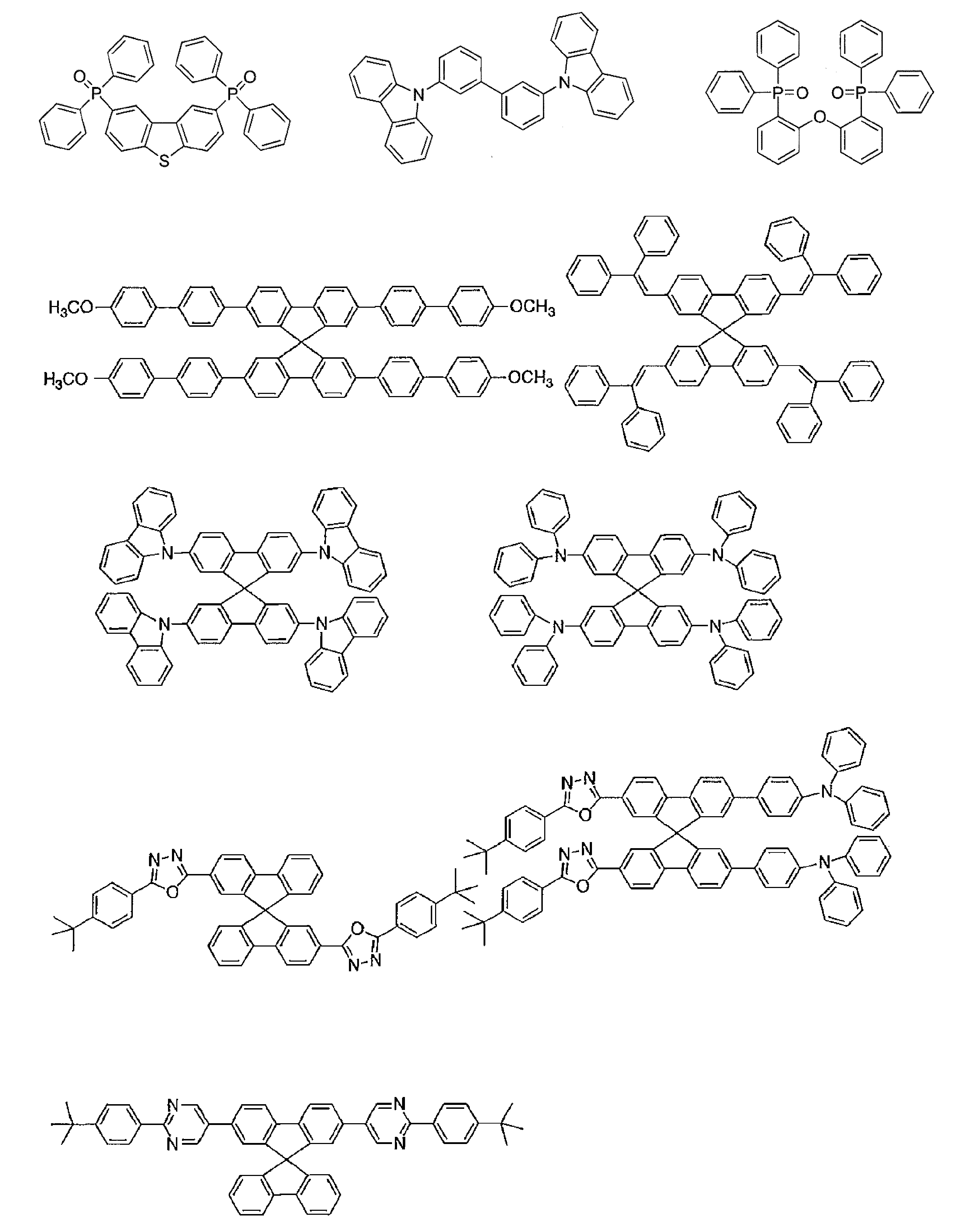


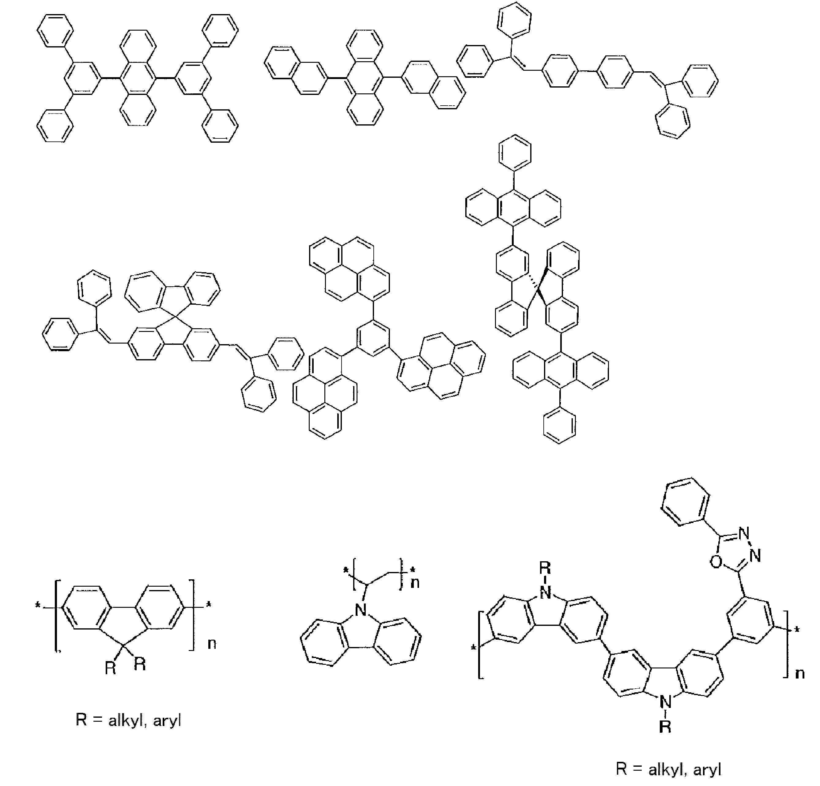

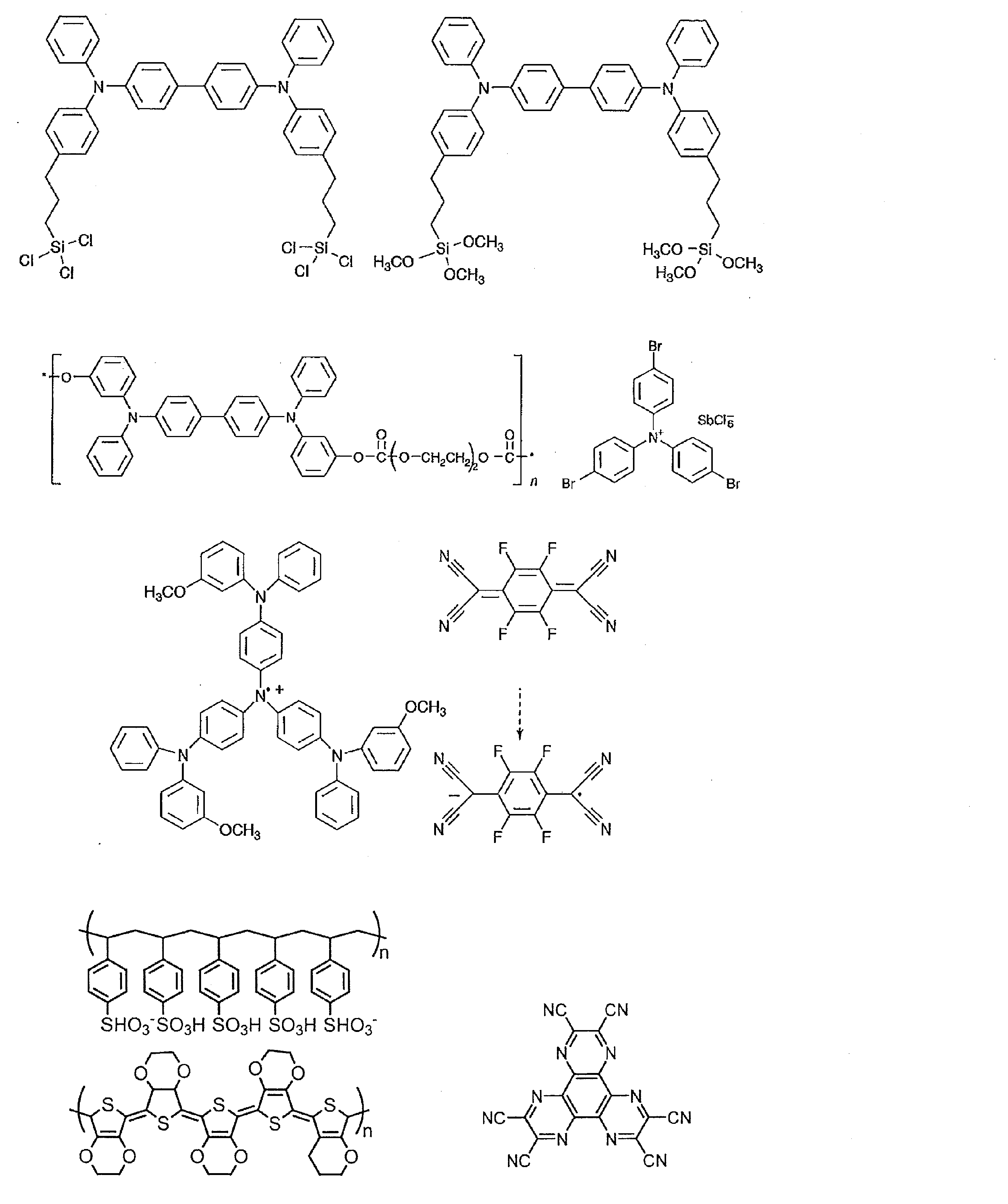
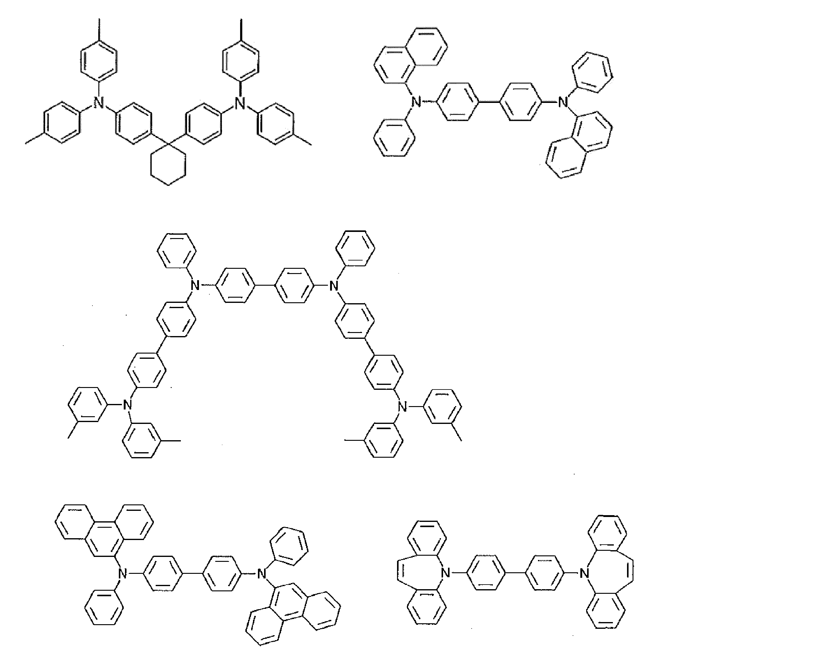


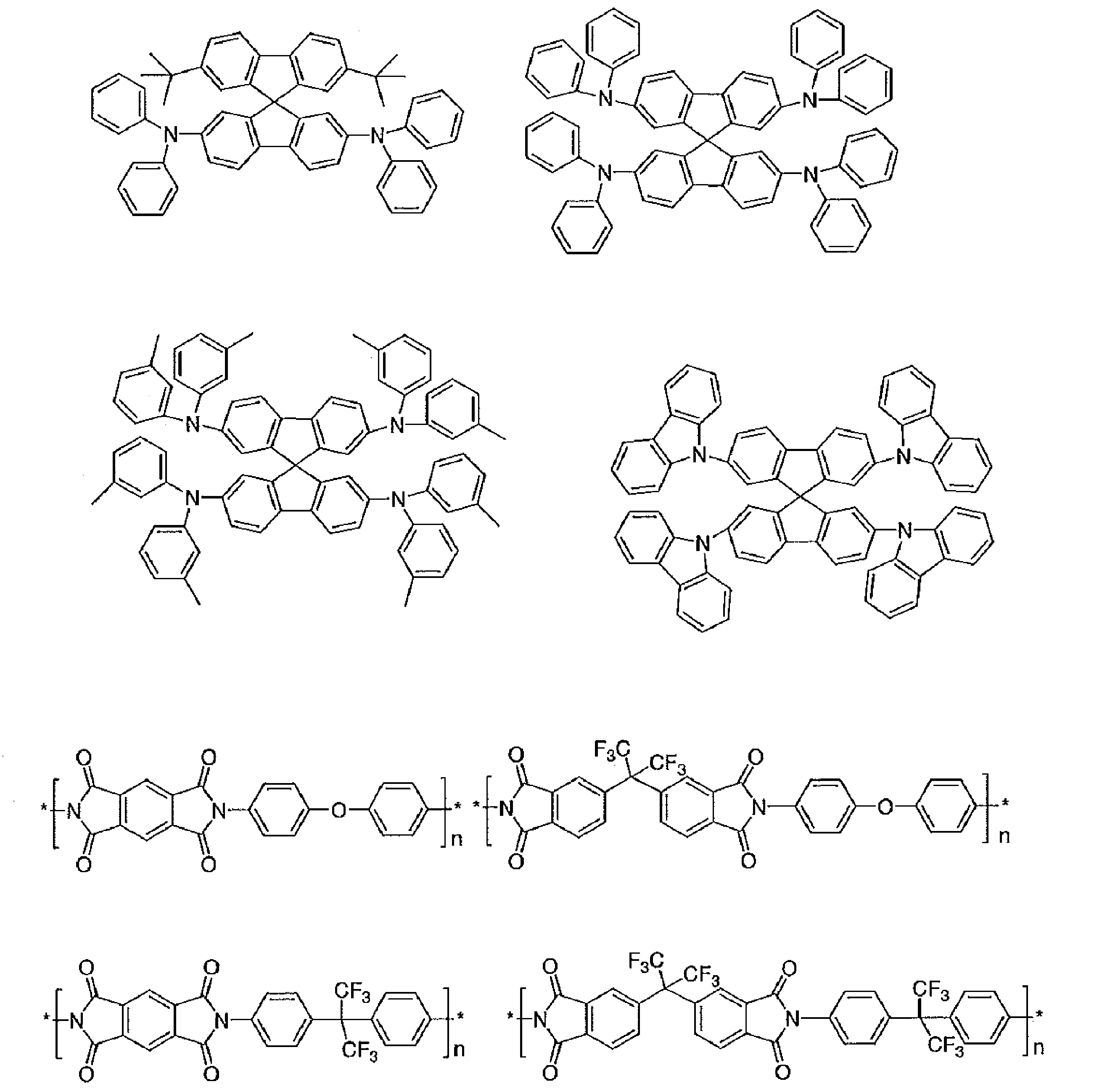

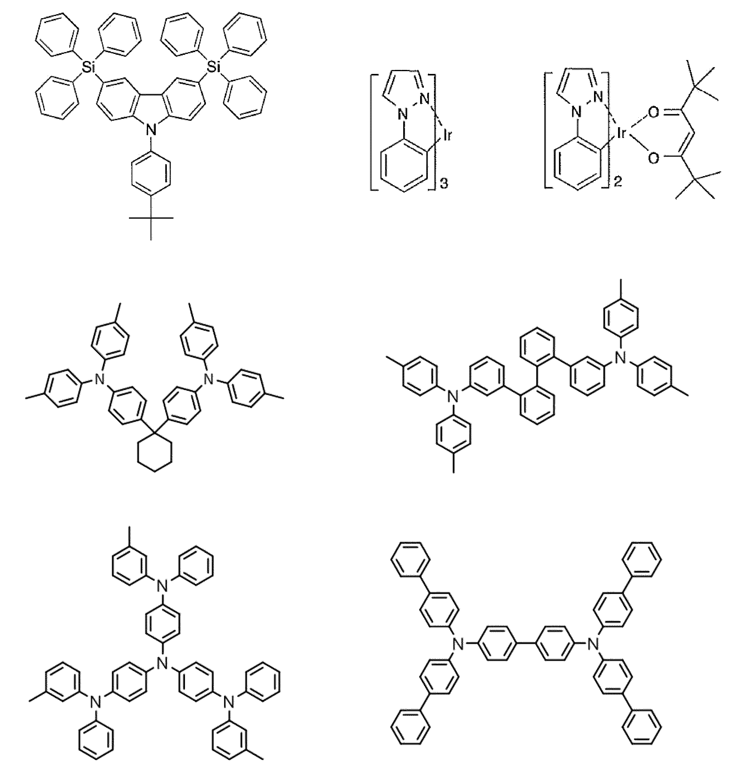
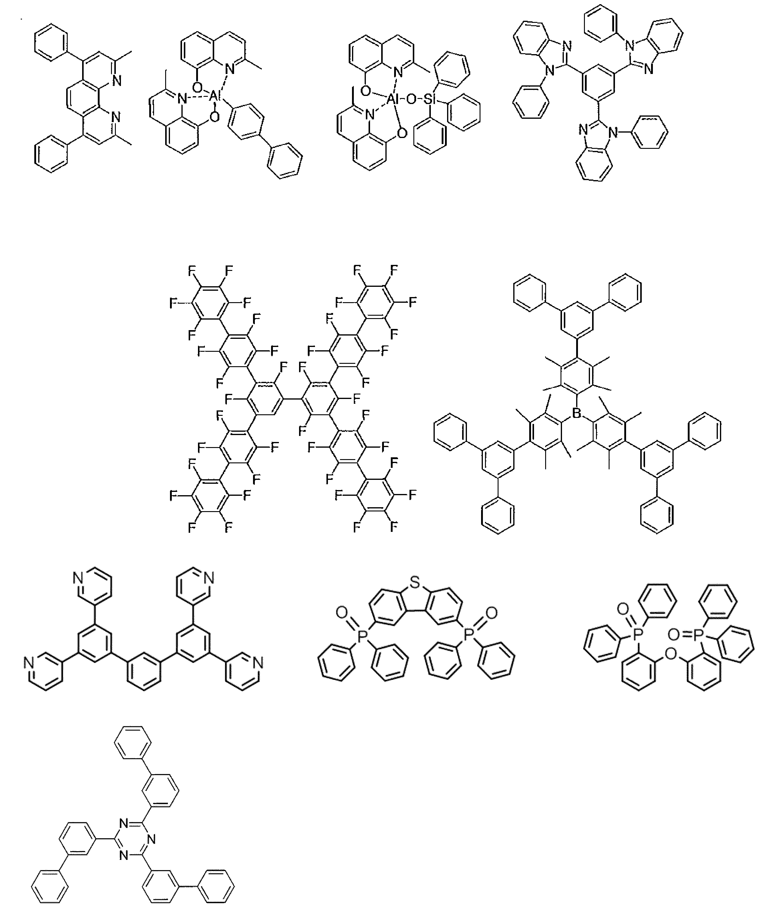


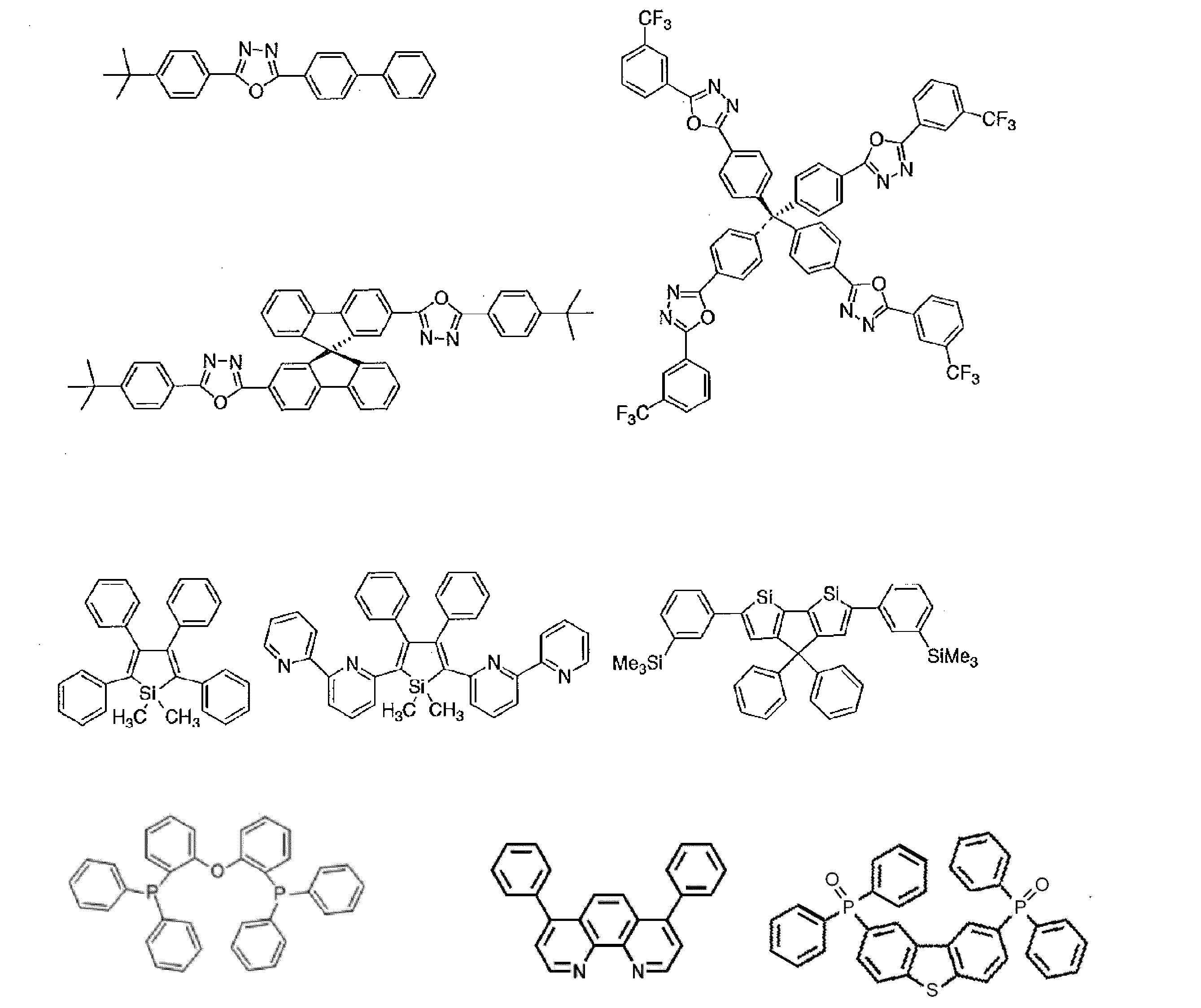


一方、燐光については、通常の有機化合物では、励起三重項エネルギーは不安定で熱等に変換され、寿命が短く直ちに失活するため、室温では殆ど観測できない。通常の有機化合物の励起三重項エネルギーを測定するためには、極低温の条件での発光を観測することにより測定可能である。 The organic electroluminescent device produced by the above-described method emits light by applying an electric field between the anode and the cathode of the obtained device. At this time, if the light is emitted by excited singlet energy, light having a wavelength corresponding to the energy level is confirmed as fluorescent light emission. At this time, delayed fluorescence may be confirmed. Further, in the case of light emission by excited triplet energy, a wavelength corresponding to the energy level is confirmed as phosphorescence. Since normal fluorescence has a shorter fluorescence lifetime than delayed fluorescence, the emission lifetime can be distinguished from fluorescence and delayed fluorescence.
On the other hand, with respect to phosphorescence, in ordinary organic compounds, the excited triplet energy is unstable and is converted into heat or the like, and the lifetime is short and it is immediately deactivated. In order to measure the excited triplet energy of a normal organic compound, it can be measured by observing light emission under extremely low temperature conditions.
以下において、アクティブ駆動方式で有機エレクトロルミネッセンス素子を駆動する有機エレクトロルミネッセンス表示装置の一例について説明する。
アクティブ駆動方式の有機エレクトロルミネッセンス表示装置は、例えば、上記の有機エレクトロルミネッセンス素子に、TFT(薄膜トランジスタ)回路、層間絶縁膜、平坦化膜および封止構造が付加されて構成される。具体的には、こうしたアクティブ駆動方式の有機エレクトロルミネッセンス表示装置は、TFT回路を備えた基板(回路基板)と、回路基板上に層間絶縁膜及び平坦化膜を介して設けられた有機エレクトロルミネッセンス素子(有機EL素子)と、有機EL素子を覆う無機封止膜と、無機封止膜上に設けられた封止基板と、基板と封止基板との間に充填された封止材とで概略構成され、封止基板側から光を取り出すトップエミッション構造とされている。
この有機エレクトロルミネッセンス表示装置で用いる有機EL素子は、基板を除いた残りの部分、すなわち、第1電極と有機EL層と第2電極からなる積層体であることとする。 [Organic electroluminescence display]
Hereinafter, an example of an organic electroluminescence display device that drives an organic electroluminescence element by an active driving method will be described.
An active drive organic electroluminescence display device is configured, for example, by adding a TFT (thin film transistor) circuit, an interlayer insulating film, a planarization film, and a sealing structure to the organic electroluminescence element. Specifically, such an organic electroluminescence display device of an active drive system includes a substrate (circuit board) provided with a TFT circuit, and an organic electroluminescence element provided on the circuit board via an interlayer insulating film and a planarizing film. (Organic EL element), an inorganic sealing film covering the organic EL element, a sealing substrate provided on the inorganic sealing film, and a sealing material filled between the substrate and the sealing substrate The top emission structure is configured to extract light from the sealing substrate side.
The organic EL element used in this organic electroluminescence display device is assumed to be the remaining portion excluding the substrate, that is, a laminate composed of the first electrode, the organic EL layer, and the second electrode.
基板としては、ガラス、石英等からなる無機材料基板;ポリエチレンテレフタレート、ポリカルバゾール、ポリイミド等からなるプラスチック基板;アルミナ等からなるセラミックス基板等の絶縁性基板や、アルミニウム(Al)、鉄(Fe)等からなる金属基板;前記基板表面に酸化シリコン(SiO2)等の有機絶縁材料等からなる絶縁物をコーティングした基板;Al等からなる金属基板の表面を陽極酸化等の方法で絶縁化処理を施した基板等が例示できるが、これらに限定されない。 The TFT substrate includes a substrate and a TFT circuit provided on the substrate.
As a substrate, an inorganic material substrate made of glass, quartz, etc .; a plastic substrate made of polyethylene terephthalate, polycarbazole, polyimide, etc .; an insulating substrate such as a ceramic substrate made of alumina, etc., aluminum (Al), iron (Fe), etc. A metal substrate comprising: a substrate coated with an insulating material made of an organic insulating material such as silicon oxide (SiO 2); the surface of a metal substrate made of Al or the like was subjected to insulation treatment by a method such as anodic oxidation Although a board | substrate etc. can be illustrated, it is not limited to these.
活性層の材料としては、非晶質シリコン(アモルファスシリコン)、多結晶シリコン(ポリシリコン)、微結晶シリコン、セレン化カドミウム等の無機半導体材料;酸化亜鉛、酸化インジウム-酸化ガリウム-酸化亜鉛等の酸化物半導体材料;ポリチオフェン誘導体、チオフエンオリゴマー、ポリ(p-フェリレンビニレン)誘導体、ナフタセン、ペンタセン等の有機半導体材料等が挙げられる。
ゲート絶縁膜は、公知の材料を用いて形成することができる。具体的には、ゲート絶縁膜の材料として、プラズマ誘起化学気相成長(PECVD)法若しくは減圧化学気相成長(LPCVD)法等により形成されたSiO2又はポリシリコン膜を熱酸化して得られたSiO2等を例示することができる。
TFTを構成するソース電極、ドレイン電極およびゲート電極、配線回路の信号電極線、走査電極線、共通電極線、第1駆動電極及び第2駆動電極は、例えば、タンタル(Ta)、アルミニウム(Al)、銅(Cu)等の公知の材料を用いて形成することができる。 The TFT has an active layer, a gate insulating film, a source electrode, a drain electrode, and a gate electrode. The type of TFT is not particularly limited, and conventionally known ones such as a staggered type, an inverted staggered type, a top gate type, and a coplanar type can be used.
As the material of the active layer, amorphous silicon (amorphous silicon), polycrystalline silicon (polysilicon), microcrystalline silicon, inorganic semiconductor materials such as cadmium selenide; zinc oxide, indium oxide-gallium oxide-zinc oxide, etc. Oxide semiconductor materials; organic semiconductor materials such as polythiophene derivatives, thiophene oligomers, poly (p-ferylene vinylene) derivatives, naphthacene, and pentacene.
The gate insulating film can be formed using a known material. Specifically, it is obtained by thermally oxidizing a SiO 2 or polysilicon film formed by a plasma induced chemical vapor deposition (PECVD) method or a low pressure chemical vapor deposition (LPCVD) method as a material of the gate insulating film. Examples thereof include SiO 2 and the like.
The source electrode, drain electrode and gate electrode constituting the TFT, signal electrode line of the wiring circuit, scanning electrode line, common electrode line, first drive electrode and second drive electrode are, for example, tantalum (Ta), aluminum (Al) It can be formed using a known material such as copper (Cu).
層間絶縁膜は、例えば、酸化シリコン(SiO2)、窒化シリコン(SiN、Si2N4)、酸化タンタル(TaO、Ta2O5)等の無機材料;アクリル樹脂、レジスト材料等の有機材料等、公知の材料を用いて形成することができる。層間絶縁膜の形成方法としては、化学気相成長(CVD)法、真空蒸着法等のドライプロセスや、スピンコート法等のウエットプロセスを例示することができ、必要に応じてフォトリソグラフィー法等によりパターニングしてもよい。
また、層間絶縁膜には遮光性を付与するか、層間絶縁膜と遮光性絶縁膜とを組み合わせて設けることが好ましい。この有機エレクトロルミネッセンス表示装置では、発光を封止基板側から取り出すために大半が光透過性の材料で構成される。このため、外光がTFT回路に入射して、TFT特性を不安定にすることが懸念される。これに対して、層間絶縁膜に遮光性を付与するか、層間絶縁膜と遮光性絶縁膜とを組み合わせ設ければ、TFT回路への外光の入射が抑えられ、安定なTFT特性を得ることができる。遮光性の層間絶縁膜および遮光性絶縁膜の材料としては、フタロシアニン、キナクロドン等の顔料又は染料をポリイミド等の高分子樹脂に分散させたものや、カラーレジスト、ブラックマトリクス材料、NixZnyFe2O4等の無機絶縁材料等を例示することができる。 The interlayer insulating film is provided so as to cover the upper surface of the substrate and the TFT circuit.
The interlayer insulating film is, for example, an inorganic material such as silicon oxide (SiO 2 ), silicon nitride (SiN, Si 2 N 4 ), tantalum oxide (TaO, Ta 2 O 5 ), or an organic material such as an acrylic resin or a resist material. It can be formed using a known material. Examples of the method for forming the interlayer insulating film include dry processes such as chemical vapor deposition (CVD) and vacuum deposition, and wet processes such as spin coating, and photolithography is used as necessary. Patterning may be performed.
In addition, the interlayer insulating film is preferably provided with a light shielding property or provided in combination with an interlayer insulating film and a light shielding insulating film. In this organic electroluminescence display device, most of the light emission is made of a light-transmitting material in order to extract light emission from the sealing substrate side. For this reason, there is a concern that external light may enter the TFT circuit and make TFT characteristics unstable. On the other hand, if the interlayer insulating film is provided with a light shielding property, or if the interlayer insulating film and the light shielding insulating film are provided in combination, the incidence of external light to the TFT circuit can be suppressed and stable TFT characteristics can be obtained. Can do. Materials for the light-shielding interlayer insulating film and the light-shielding insulating film include those obtained by dispersing pigments or dyes such as phthalocyanine and quinaclonone in polymer resins such as polyimide, color resists, black matrix materials, NixZnyFe 2 O 4, etc. Inorganic insulating materials and the like can be exemplified.
平坦化膜は、特に限定されないが、例えば、酸化シリコン、窒化シリコン、酸化タンタル等の無機材料や、ポリイミド、アクリル樹脂、レジスト材料等の有機材料等の公知の材料を用いて形成することができる。平坦化膜の形成方法としては、CVD法、真空蒸着法等のドライプロセスや、スピンコート法等のウエットプロセスを例示することができるが、これらの方法に限定されるものではない。また、平坦化膜は、単層構造及び多層構造のいずれであってもでもよい。 The planarizing film is provided on the interlayer insulating film. The planarization film has a defect in the organic EL element (for example, a defect in the first electrode or the organic EL layer, a disconnection in the second electrode, a short circuit between the first electrode and the second electrode, or a breakdown voltage due to unevenness on the surface of the TFT circuit. This is provided in order to prevent the occurrence of a decrease or the like. Note that the planarization film can be omitted.
The planarizing film is not particularly limited, and can be formed using a known material such as an inorganic material such as silicon oxide, silicon nitride, or tantalum oxide, or an organic material such as polyimide, acrylic resin, or resist material. . Examples of the method for forming the planarizing film include a dry process such as a CVD method and a vacuum deposition method, and a wet process such as a spin coating method, but are not limited to these methods. Further, the planarization film may have either a single layer structure or a multilayer structure.
有機EL素子の第1電極は、各画素に対応するように、X-Yマトリクス状に複数個配置されており、TFTのドレイン電極に接続されている。この第1電極は有機エレクトロルミネッセンス表示装置の画素電極として機能する。第1電極は、発光部からの発光の取り出し効率を向上させるために、光の反射率が高い電極(反射電極)を用いることが好ましい。このような電極としては、アルミニウム、銀、金、アルミニウム-リチウム合金、アルミニウム-ネオジウム合金、アルミニウム-シリコン合金等の光反射性金属電極や、透明電極と前記光反射性金属電極(反射電極)とを組み合わせた電極等を例示することができる。 The organic EL element includes a first electrode, an organic EL layer, and a second electrode, and is provided on the planarizing film with the first electrode side set as the planarizing film side. However, when the planarizing film is not provided, the organic EL element is provided on the interlayer insulating film with the first electrode side set as the interlayer insulating film side.
A plurality of first electrodes of the organic EL element are arranged in an XY matrix so as to correspond to each pixel, and are connected to the drain electrode of the TFT. The first electrode functions as a pixel electrode of the organic electroluminescence display device. The first electrode is preferably an electrode (reflecting electrode) having a high light reflectance in order to improve the efficiency of extracting light emitted from the light emitting unit. Examples of such electrodes include light reflective metal electrodes such as aluminum, silver, gold, aluminum-lithium alloys, aluminum-neodymium alloys, and aluminum-silicon alloys, and transparent electrodes and the light reflective metal electrodes (reflective electrodes). The electrode etc. which combined can be illustrated.
エッジカバーの膜厚は、100~2000nmであることが好ましい。エッジカバーの膜厚が100nm以上であることにより、十分な絶縁性が得られ、第1電極と第2電極との間のリークに伴う消費電力の上昇や非発光の発生を効果的に抑制することができる。また、エッジカバーの膜厚が2000nm以下であることにより、成膜プロセスでの生産性の低下や、エッジカバーにおける第2電極の断線を効果的に抑制することができる。 In addition, an edge cover made of an insulating material is provided at an end portion along the edge of each first electrode. Thereby, it is possible to prevent a leak from occurring between the first electrode and the second electrode. The edge cover is formed by depositing an insulating material by a known method such as an EB vapor deposition method, a sputtering method, an ion plating method, or a resistance heating vapor deposition method, and then patterned by a known photolithography method using dry etching or wet etching. Can be formed. Examples of the insulating material constituting the edge cover include known materials having optical transparency such as SiO, SiON, SiN, SiOC, SiC, HfSiON, ZrO, HfO, and LaO.
The film thickness of the edge cover is preferably 100 to 2000 nm. When the film thickness of the edge cover is 100 nm or more, sufficient insulation can be obtained, and an increase in power consumption and non-light emission caused by leakage between the first electrode and the second electrode can be effectively suppressed. be able to. Moreover, when the film thickness of the edge cover is 2000 nm or less, it is possible to effectively suppress a decrease in productivity in the film forming process and disconnection of the second electrode in the edge cover.
封止基板としては、回路基板で用いる基板と同様のものを用いることができるが、封止基板側から発光を取り出すため、光透過性を有することが必要である。また、封止基板には、色純度を高めるために、カラーフィルタが設けられていてもよい。 A sealing substrate is provided on the inorganic sealing film, and a sealing material is filled around the organic EL element disposed between the circuit substrate and the sealing substrate. Thereby, external oxygen and moisture are prevented from entering the organic EL layer, and the life of the organic electroluminescence display device can be extended.
As the sealing substrate, a substrate similar to the substrate used for the circuit substrate can be used. However, in order to extract light emission from the sealing substrate side, it is necessary to have light transmittance. In addition, a color filter may be provided on the sealing substrate in order to increase color purity.
また、封止材として窒素ガス、アルゴンガス等の不活性ガスを用いてもよく、この場合、窒素ガス、アルゴンガス等の不活性ガスをガラス等の封止基板で封止する方法が挙げられる。さらにこの場合には、水分による有機EL部の劣化を効果的に抑制するために、不活性ガスと共に酸化バリウム等の吸湿剤を封入することが好ましい。 The sealing material can be formed by a known method using a known sealing material. As a sealing material, what consists of resin (curable resin) can be illustrated. In this case, for example, a curable resin composition (photocurable resin composition) is formed on the upper surface and / or side surface of the inorganic sealing film of the substrate on which the organic EL element and the inorganic sealing film are formed, or on the sealing substrate. Material, thermosetting resin composition) by spin coating method, laminating method, etc., the substrate and the sealing substrate are bonded together through this coating layer, and the curable resin composition is photocured or thermally cured. By curing, a sealing material can be formed. Note that the sealing material needs to have light transmittance.
Moreover, you may use inert gas, such as nitrogen gas and argon gas, as a sealing material, In this case, the method of sealing inert gas, such as nitrogen gas and argon gas, with sealing substrates, such as glass, is mentioned. . Furthermore, in this case, in order to effectively suppress deterioration of the organic EL part due to moisture, it is preferable to enclose a moisture absorbent such as barium oxide together with an inert gas.
また、本実施例では、発光寿命が0.05μs以上の蛍光を遅延蛍光として判定した。
なお、以下に掲載する発光素子の層構成を示す表における「厚み」の単位はnmである。また、単一層の中に2種以上の材料が含まれている場合は、ホスト材料を「材料1」とし、ドーパント材料を「材料2」として表示している。3成分系の場合は、便宜上ホスト材料を「材料1」とし、それ以外の2成分を「材料2」として表示している。また、「材料2」の欄に層中における材料2の濃度(単位:重量%}を表示している。表中の「HIL」はホール注入層、「HTL」はホール輸送層、「EBL」は電子阻止層、「INT」は隔離層、「ASL」は励起子生成層、「EML」は発光層、「HBL」はホール阻止層、「ETL」は電子輸送層を示す。 The features of the present invention will be described more specifically with reference to the following examples. The following materials, processing details, processing procedures, and the like can be changed as appropriate without departing from the spirit of the present invention. Therefore, the scope of the present invention should not be construed as being limited by the specific examples shown below. Note that the evaluation of the light emission characteristics is as follows: source meter (manufactured by Keithley: 2400 series), semiconductor parameter analyzer (manufactured by Agilent Technologies: E5273A), optical power meter measuring device (manufactured by Newport: 1930C), optical spectrometer (Ocean Optics, USB2000), spectroradiometer (Topcon, SR-3) and streak camera (Hamamatsu Photonics C4334) were used.
In this example, fluorescence having a light emission lifetime of 0.05 μs or more was determined as delayed fluorescence.
The unit of “thickness” in the table showing the layer structure of the light-emitting element described below is nm. When two or more kinds of materials are contained in a single layer, the host material is indicated as “
膜厚100nmのインジウム・スズ酸化物(ITO)からなる陽極が形成されたガラス基板上に、各薄膜を真空蒸着法にて、真空度2×10⁻⁵Paで積層した。
まず、ITO上にHAT-CNを10nmの厚さに蒸着して正孔注入層を形成し、その上に、TrisPCzを30nmの厚さに蒸着して正孔輸送層を形成した。続いて、mCBPを6.5nmの厚さに蒸着して電子阻止層を形成した。
次に、TBRbとmCBPを異なる蒸着源から共蒸着し、5nmの厚さの発光層を形成した。この時、TBRbの濃度は1重量%とした。その上に、4CzIPNMeとmCBPを異なる蒸着源から共蒸着し、10nmの厚さの励起子生成層を形成した。この時、4CzIPNMeの濃度は10重量%とした。
次に、T2Tを12nmの厚さに蒸着して正孔阻止層を形成し、その上に、BpyTP2を55nmの厚さに蒸着して電子輸送層を形成した。さらにLiqを1nmの厚さに形成し、次いでアルミニウム(Al)を100nmの厚さに形成することにより陰極を形成した。
以上の工程により、表1に示す層構成を有する実施例1の有機エレクトロルミネッセンス素子を作製した。 (Example 1)
Each thin film was laminated at a vacuum degree of 2 × 10 −5 Pa by a vacuum deposition method on a glass substrate on which an anode made of indium tin oxide (ITO) having a thickness of 100 nm was formed.
First, HAT-CN was deposited on ITO to a thickness of 10 nm to form a hole injection layer, and then TrisPCz was deposited to a thickness of 30 nm to form a hole transport layer. Subsequently, mCBP was evaporated to a thickness of 6.5 nm to form an electron blocking layer.
Next, TBRb and mCBP were co-evaporated from different deposition sources to form a light-emitting layer having a thickness of 5 nm. At this time, the concentration of TBRb was 1% by weight. On top of that, 4CzIPNMe and mCBP were co-deposited from different deposition sources to form an exciton generation layer having a thickness of 10 nm. At this time, the concentration of 4CzIPNMe was 10% by weight.
Next, T2T was vapor-deposited to a thickness of 12 nm to form a hole blocking layer, and BpyTP2 was vapor-deposited to a thickness of 55 nm thereon to form an electron transport layer. Further, Liq was formed to a thickness of 1 nm, and then aluminum (Al) was formed to a thickness of 100 nm to form a cathode.
Through the above steps, an organic electroluminescent element of Example 1 having the layer configuration shown in Table 1 was produced.
発光層におけるTBRbの濃度を表1に示すように変えたこと以外は、実施例1と同様にして有機エレクトロルミネッセンス素子を作製した。 (Examples 2 to 8)
An organic electroluminescence element was produced in the same manner as in Example 1 except that the concentration of TBRb in the light emitting layer was changed as shown in Table 1.
実施例1と同様の方法により、比較例1の有機エレクトロルミネッセンス素子を作製した。ただし、励起子生成層は形成せず、発光層は4CzIPNMeとTBRbとmCBPとを異なる蒸着源から共蒸着して15nmの厚さの層とした。また、発光層を形成する際、4CzIPNMeの濃度は10重量%とし、TBRbの濃度は1重量%とした。比較例1の有機エレクトロルミネッセンス素子の層構成は表1に示すとおりである。 (Comparative Example 1)
By the same method as in Example 1, an organic electroluminescence element of Comparative Example 1 was produced. However, the exciton generation layer was not formed, and the light emitting layer was a layer having a thickness of 15 nm by co-evaporating 4CzIPNMe, TBRb, and mCBP from different evaporation sources. In forming the light emitting layer, the concentration of 4CzIPNMe was 10% by weight, and the concentration of TBRb was 1% by weight. The layer structure of the organic electroluminescence element of Comparative Example 1 is as shown in Table 1.
発光層におけるTBRbの濃度を表1に示すように変えたこと以外は、比較例1と同様にして有機エレクトロルミネッセンス素子を作製した。
各実施例および各比較例で使用した4CzIPNMeのΔESTは0.02eVであった。 (Comparative Examples 2 to 8)
An organic electroluminescence device was produced in the same manner as in Comparative Example 1 except that the TBRb concentration in the light emitting layer was changed as shown in Table 1.
The ΔE ST of 4CzIPNMe used in each example and each comparative example was 0.02 eV.
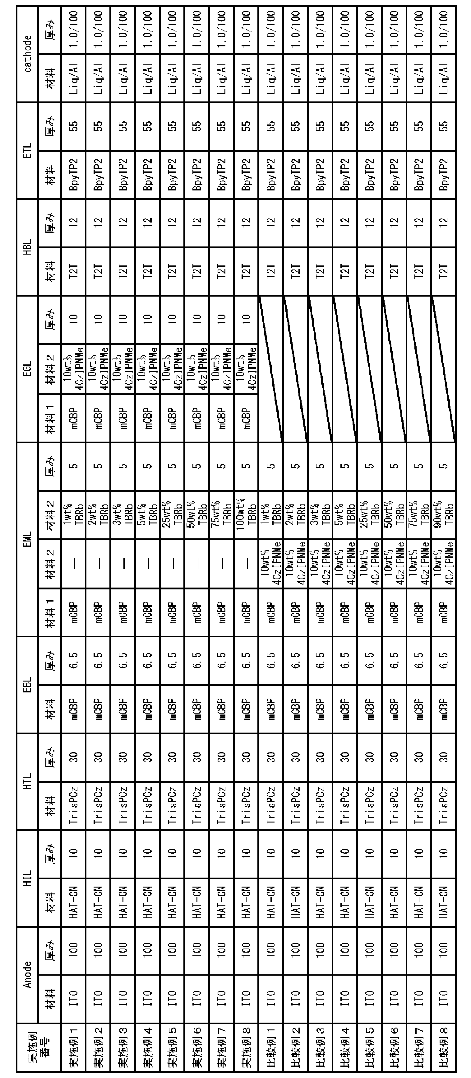
また、各実施例で作製した有機エレクトロルミネッセンス素子について、1000cd/m2で測定した発光ピーク波長、外部量子効率、色度座標(x,y)を表2に示し、比較例で作製した有機エレクトロルミネッセンス素子について、1000cd/m2で測定した発光ピーク波長、外部量子効率、色度座標(x,y)を表3に示す。 When the transient decay curve of the light emission intensity was measured for the organic electroluminescence elements prepared in each Example and each Comparative Example, delayed fluorescence could be confirmed in all cases.
Further, the organic electroluminescent device produced in each example, shows emission peak wavelength measured in 1000 cd / m 2, the external quantum efficiency, the chromaticity coordinates (x, y) in Table 2, the organic electroluminescence prepared in Comparative Example Table 3 shows the emission peak wavelength, external quantum efficiency, and chromaticity coordinates (x, y) measured at 1000 cd / m 2 for the luminescence element.


さらに、各実施例および各比較例で作製した有機エレクトロルミネッセンス素子のうち、発光層におけるTBRb濃度が25重量%、50重量%、75重量%であるもの(実施例5~実施例7で作製した素子、比較例5~7で作製した素子)について、初期輝度を約1000cd/m2に調整して定電流で連続駆動を行い、輝度が初期輝度の95%になるまでの時間LT95%を測定した。LT95%の測定結果を表4に示す。 In Tables 2 and 3, when comparing the elements having the same TbRB concentration in the light emitting layer, the organic electroluminescent elements of Examples 1 to 8 are all the corresponding organic electroluminescent elements of Comparative Examples 1 to 8. In comparison, the external quantum efficiency is high, the peak wavelength of light emission is short, and the blue purity is high. Further, when the maximum external quantum efficiency of the organic electroluminescence elements of Examples 1 to 8 was measured, a preferable result exceeding 10% was obtained. In particular, the maximum external quantum efficiency of the organic electroluminescence elements of Examples 1 to 4 was 13 More favorable results were shown at ˜14%.
Further, among the organic electroluminescence elements produced in each Example and each Comparative Example, those having a TBRb concentration in the light emitting layer of 25% by weight, 50% by weight, and 75% by weight (produced in Examples 5 to 7). Device, the device manufactured in Comparative Examples 5 to 7), the initial luminance is adjusted to about 1000 cd / m 2 and continuously driven at a constant current, and the time LT 95% until the luminance reaches 95% of the initial luminance is measured. did. Table 4 shows the measurement results of LT95%.
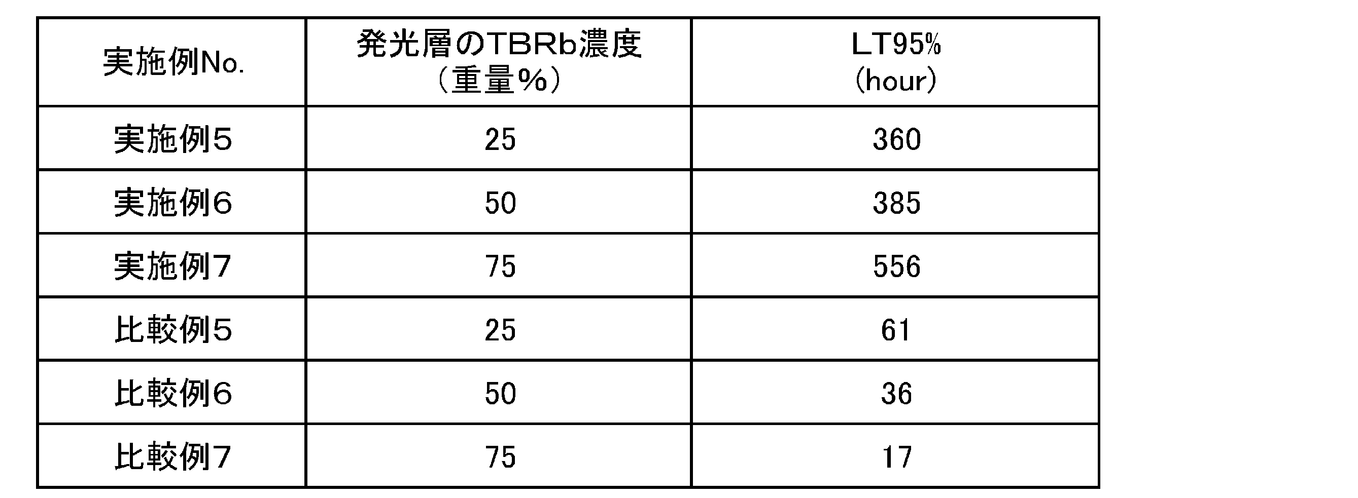
これらのことから、ΔESTが0.3以下である化合物を含む励起子生成層と発光材料を含む発光層を別の層として形成することにより、これらをともに含む単一の発光層を設ける場合に比べて、有機エレクトロルミネッセンス素子の効率と寿命が大きく改善されることがわかった。 In Table 4, when the elements having the same TbRB concentration in the light emitting layer are compared, the organic electroluminescent elements of Examples 5 to 8 are all LT95% as compared with the corresponding organic electroluminescent elements of Comparative Examples 5 to 8. Is remarkably long and has a long life.
From these, by forming a luminescent layer comprising a luminescent material and exciton generating layer containing a compound Delta] E ST is 0.3 or less as a separate layer, in the case of providing a single light emitting layer containing these together Compared to the above, it was found that the efficiency and lifetime of the organic electroluminescence device were greatly improved.
実施例1と同様の方法により、実施例9~12の有機エレクトロルミネッセンス素子を作製した。ただし、電子ブロック層と発光層の間に、電子ブロック層側から順に励起子生成層と隔離層を形成し、発光層と正孔ブロック層の間に、発光層側から順に隔離層、励起子生成層、隔離層を形成した。実施例9~12の各有機エレクトロルミネッセンス素子の層構成は下の表に示すとおりである。 (Examples 9 to 12)
In the same manner as in Example 1, organic electroluminescent elements of Examples 9 to 12 were produced. However, an exciton generating layer and a separating layer are formed in order from the electron blocking layer side between the electron blocking layer and the light emitting layer, and a separating layer and exciton are sequentially formed between the light emitting layer and the hole blocking layer from the light emitting layer side. A production layer and a separation layer were formed. The layer structure of each organic electroluminescence element of Examples 9 to 12 is as shown in the table below.

実施例の電流密度を比較すると、励起子生成層と発光層の間に形成した2つの隔離層の厚みが2nmである実施例10、11の有機エレクトロルミネッセンス素子よりも、隔離層の厚みが1nmである実施例9、12の有機エレクトロルミネッセンス素子の方が高い電流密度が得られている。このことから、励起子生成層と発光層の間に形成する隔離層の厚みは2nmよりも薄い方が好ましいことがわかった。
実施例9~12の有機エレクトロルミネッセンス素子の最大外部量子効率は13~14%であり、いずれも高い発光効率が認められた。 The emission peak wavelength was 546.0 nm for the organic electroluminescence element of Example 9, 545.0 nm for the organic electroluminescence element of Example 10, 545.8 nm for the organic electroluminescence element of Example 11, and the organic electroluminescence of Example 12. It was 548.1 nm by the luminescence element.
Comparing the current densities of the examples, the thickness of the isolation layer is 1 nm as compared with the organic electroluminescence elements of Examples 10 and 11 in which the thickness of the two isolation layers formed between the exciton generation layer and the light emitting layer is 2 nm. In the organic electroluminescence elements of Examples 9 and 12, the higher current density is obtained. From this, it was found that the thickness of the isolation layer formed between the exciton generation layer and the light emitting layer is preferably thinner than 2 nm.
The maximum external quantum efficiencies of the organic electroluminescence elements of Examples 9 to 12 were 13 to 14%, and high luminous efficiency was recognized in all cases.
実施例1と同様の方法により、比較例9、実施例13、実施例14の各有機エレクトロルミネッセンス素子を作製した。ただし、実施例13と実施例14では、励起子生成層とホールブロック層の間に発光層を形成した。比較例9、実施例13、実施例14の各有機エレクトロルミネッセンス素子の層構成は下の表に示すとおりである。 (Comparative Example 9, Example 13, Example 14)
By the same method as Example 1, each organic electroluminescent element of Comparative Example 9, Example 13, and Example 14 was produced. However, in Example 13 and Example 14, the light emitting layer was formed between the exciton generation layer and the hole blocking layer. The layer structure of each organic electroluminescent element of Comparative Example 9, Example 13, and Example 14 is as shown in the table below.

また、各有機エレクトロルミネッセンス素子の電流密度-外部量子効率特性を図2に示す。比較例9に比べて、実施例13と実施例14の各有機エレクトロルミネッセンス素子は、高い発光効率を示した。このことから、励起子発生層を形成することにより発光効率が向上することが確認された。 For each of the organic electroluminescent elements of Comparative Example 9, Example 13, and Example 14, the transient decay curve of the light emission intensity was measured, and all of the delayed fluorescence could be confirmed.
In addition, FIG. 2 shows current density-external quantum efficiency characteristics of each organic electroluminescence element. Compared to Comparative Example 9, each of the organic electroluminescent elements of Example 13 and Example 14 showed higher luminous efficiency. From this, it was confirmed that the luminous efficiency is improved by forming the exciton generation layer.
酢酸亜鉛1g、モノエタノールアミン0.28g、2-メトキシエタノール10mlの混合物を室温で一晩攪拌した後に、膜厚100nmのインジウム・スズ酸化物(ITO)からなる陰極が形成されたガラス基板上にスピンコーティングした(5000rpm、60秒)。その後、200℃で10分間アニーリングすることにより電子注入層を形成した。その上に、量子ドットのトルエン溶液(Aldrich製、型番753785、粒径6nm、濃度1mg/ml、蛍光ピーク波長575nm)をスピンコーティング(1000rpm、60秒)し、100℃で10分間アニーリングすることにより約12nmの厚さの発光層を形成した。その後、以下の薄膜を真空蒸着法にて、真空度2×10-5Paで積層した。まず、4CzIPNとmCBPを異なる蒸着源から共蒸着し、15nmの厚さの励起子発生層を形成した。この時、4CzIPNの濃度は20%とした。次いで、mCBPを5nmの厚さに蒸着して電子阻止層を形成し、その上にTrisPCzを30nmの厚さに蒸着して正孔輸送層を形成した。続いて、HAT-CNを20nmの厚さに蒸着して正孔注入層を形成し、次いでアルミニウム(Al)を100nmの厚さに形成することにより陽極を形成した。
以上の工程により、表7に示す層構成を有する実施例15の有機エレクトロルミネッセンス素子を作製した。
実施例15で使用した4CzIPNのΔESTは0.06eVであった。 (Example 15)
A mixture of 1 g of zinc acetate, 0.28 g of monoethanolamine and 10 ml of 2-methoxyethanol was stirred overnight at room temperature, and then on a glass substrate on which a cathode made of indium tin oxide (ITO) having a thickness of 100 nm was formed. Spin coated (5000 rpm, 60 seconds). Then, the electron injection layer was formed by annealing for 10 minutes at 200 degreeC. On top of that, spin solution (1000 rpm, 60 seconds) of a quantum dot toluene solution (Aldrich, model number 753785, particle size 6 nm,
Through the above steps, an organic electroluminescent element of Example 15 having the layer configuration shown in Table 7 was produced.
The ΔE ST of 4CzIPN used in Example 15 was 0.06 eV.
実施例15と同様の方法により、比較例10の有機エレクトロルミネッセンス素子を作製した。ただし、励起子発生層に相当する層を形成する際には4CzIPNを共蒸着させず、mCBPのみからなる層を15nm形成した。比較例10の有機エレクトロルミネッセンス素子の層構成は表7に示すとおりである。 (Comparative Example 10)
In the same manner as in Example 15, an organic electroluminescence element of Comparative Example 10 was produced. However, when the layer corresponding to the exciton generation layer was formed, 4 CzIPN was not co-evaporated, and a layer made of mCBP alone was formed to 15 nm. The layer configuration of the organic electroluminescence element of Comparative Example 10 is as shown in Table 7.

各有機エレクトロルミネッセンス素子の外部量子効率を0.1mA/cm2で測定したところ、比較例10では3.5%であったのに対して、実施例15では5%と高い値を示した。このことから、量子ドットを用いた有機エレクトロルミネッセンス素子においても、励起子発生層を形成することにより発光効率が向上することが確認された。 For each of the organic electroluminescence elements of Example 15 and Comparative Example 10, the emission intensity transient decay curve was measured. As a result, delayed fluorescence was confirmed for Example 15, but delayed fluorescence was confirmed for Comparative Example 10. I could not.
When the external quantum efficiency of each organic electroluminescence device was measured at 0.1 mA / cm 2 , it was 3.5% in Comparative Example 10 and a high value of 5% in Example 15. From this, it was confirmed that even in the organic electroluminescence device using quantum dots, the luminous efficiency is improved by forming the exciton generation layer.
実施例1と同様の方法により、陽極、正孔注入層、正孔輸送第1層、正孔輸送第2層、電子阻止層、励起子生成層、隔離層、発光層、正孔阻止層、電子輸送層、陰極を順に形成することにより、実施例16の有機エレクトロルミネッセンス素子を作製した。この素子の層構成は表8に示すとおりである。 (Example 16)
In the same manner as in Example 1, the anode, hole injection layer, hole transport first layer, hole transport second layer, electron blocking layer, exciton generation layer, isolation layer, light emitting layer, hole blocking layer, An organic electroluminescence device of Example 16 was produced by sequentially forming an electron transport layer and a cathode. The layer structure of this element is as shown in Table 8.
実施例16と同様の方法により、比較例11の有機エレクトロルミネッセンス素子を作製した。ただし、実施例16の隔離層、発光層、正孔阻止層のかわりに総厚が同じ正孔阻止層を1層形成し、その他の層構成は実施例16と同じにした。この比較例11の有機エレクトロルミネッセンス素子の層構成は表8に示すとおりである。実施例16における励起子生成層は、比較例11では発光層として機能する。 (Comparative Example 11)
In the same manner as in Example 16, an organic electroluminescence element of Comparative Example 11 was produced. However, one hole blocking layer having the same total thickness was formed instead of the isolation layer, the light emitting layer, and the hole blocking layer of Example 16, and the other layer configuration was the same as that of Example 16. The layer structure of the organic electroluminescence element of Comparative Example 11 is as shown in Table 8. The exciton generating layer in Example 16 functions as a light emitting layer in Comparative Example 11.

各有機エレクトロルミネッセンス素子の外部量子効率を0.1mA/cm2で測定したところ、比較例11では13.1%であったのに対して、実施例16では13.4%と高い値を示した。このことから、遅延蛍光材料をアシストドーパントとして用いた励起子発生層を形成した場合においても、発光効率が向上することが確認された。 When the transient decay curve of the light emission intensity was measured for each of the organic electroluminescence elements of Example 16 and Comparative Example 11, delayed fluorescence was confirmed for each element. In addition, the emission peak wavelength was the same for all elements.
When the external quantum efficiency of each organic electroluminescence element was measured at 0.1 mA / cm 2 , it was 13.1% in Comparative Example 11, whereas it was as high as 13.4% in Example 16. It was. From this, it was confirmed that the luminous efficiency was improved even when an exciton generation layer using a delayed fluorescent material as an assist dopant was formed.
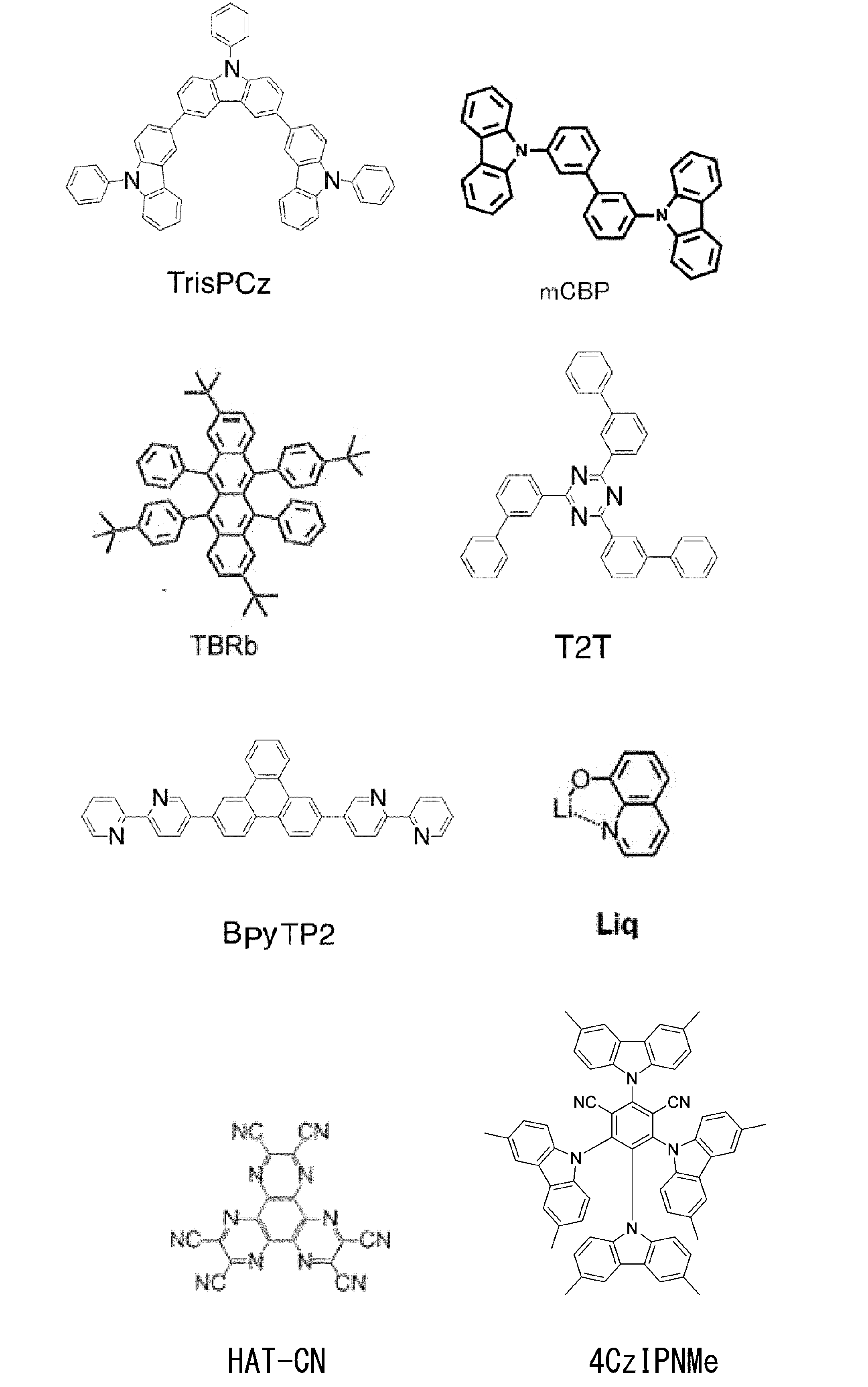
2 陽極
3 正孔注入層
4 正孔輸送層
5 発光部
6 電子輸送層
7 陰極 DESCRIPTION OF
Claims (15)
- 下記式(1)を満たす化合物または遅延蛍光を発するエキサイプレックスを含む励起子生成層と発光材料を含む発光層を有する有機発光素子。
ΔEST ≦ 0.3eV (1)
(上式において、ΔESTは、最低励起一重項エネルギー準位ES1と最低励起三重項エネルギー準位ET1の差である。) An organic light emitting device having an exciton generation layer including a compound satisfying the following formula (1) or an exciplex emitting delayed fluorescence and a light emitting layer including a light emitting material.
ΔE ST ≦ 0.3eV (1)
(In the above equation, ΔE ST is the difference between the lowest excited singlet energy level E S1 and the lowest excited triplet energy level E T1 .) - 前記励起子生成層と前記発光層の間に隔離層を有する、請求項1に記載の有機発光素子。 The organic light emitting device according to claim 1, further comprising an isolation layer between the exciton generation layer and the light emitting layer.
- 前記発光層の陽極側および陰極側のいずれか一方に前記励起子生成層を有する、請求項1または2に記載の有機発光素子。 The organic light emitting element according to claim 1 or 2, wherein the exciton generation layer is provided on either the anode side or the cathode side of the light emitting layer.
- 前記発光層の陽極側と陰極側にそれぞれ前記励起子生成層を有する、請求項1または2に記載の有機発光素子。 The organic light emitting element according to claim 1 or 2, wherein the exciton generation layer is provided on each of an anode side and a cathode side of the light emitting layer.
- 前記発光層とその発光層よりも陽極側に形成された励起子生成層の間に第1隔離層を有し、前記発光層とその発光層よりも陰極側に形成された励起子生成層の間に第2隔離層を有する、請求項4に記載の有機発光素子。 A first isolation layer between the light emitting layer and an exciton generating layer formed on the anode side of the light emitting layer, and an exciton generating layer formed on the cathode side of the light emitting layer and the light emitting layer. The organic light emitting device according to claim 4, further comprising a second isolation layer therebetween.
- 前記励起子生成層の陽極側と陰極側にそれぞれ前記発光層を有する、請求項1または2に記載の有機発光素子。 The organic light emitting device according to claim 1 or 2, wherein the light emitting layer is provided on each of an anode side and a cathode side of the exciton generation layer.
- 前記励起子生成層とその励起子生成層よりも陽極側に形成された発光層の間に第1隔離層を有し、前記励起子生成層とその励起子生成層よりも陰極側に形成された発光層の間に第2隔離層を有する、請求項6に記載の有機発光素子。 A first isolation layer is provided between the exciton generation layer and the light emitting layer formed on the anode side of the exciton generation layer, and is formed on the cathode side of the exciton generation layer and the exciton generation layer. The organic light emitting device according to claim 6, further comprising a second isolation layer between the light emitting layers.
- 前記第1隔離層と前記第2隔離層がキャリア輸送性化合物を含む、請求項5または7に記載の有機発光素子(ただし、前記キャリア輸送性化合物は、前記式(1)を満たす化合物、前記遅延蛍光を発するエキサイプレックス、前記発光材料のいずれとも異なる化合物である。)。 The organic light-emitting device according to claim 5 or 7, wherein the first isolation layer and the second isolation layer include a carrier transporting compound (wherein the carrier transporting compound is a compound satisfying the formula (1), Exciplex that emits delayed fluorescence and a compound different from any of the light emitting materials).
- 前記発光層がキャリア輸送性化合物を含む、請求項1~8のいずれか1項に記載の有機発光素子(ただし、前記キャリア輸送性化合物は、前記式(1)を満たす化合物、前記遅延蛍光を発するエキサイプレックス、前記発光材料のいずれとも異なる化合物である。)。 The organic light-emitting device according to any one of claims 1 to 8, wherein the light-emitting layer contains a carrier transporting compound (wherein the carrier transporting compound is a compound satisfying the formula (1), the delayed fluorescence) Exciplex to be emitted, and a compound different from any of the light emitting materials.
- 前記励起子生成層(複数の励起子生成層がある場合は少なくとも1層の励起子生成層)がキャリア輸送性化合物を含む、請求項1~9のいずれか1項に記載の有機発光素子(ただし、前記キャリア輸送性化合物は、前記式(1)を満たす化合物、前記遅延蛍光を発するエキサイプレックス、前記発光材料のいずれとも異なる化合物である。)。 The organic light-emitting device according to any one of claims 1 to 9, wherein the exciton generation layer (at least one exciton generation layer when there are a plurality of exciton generation layers) includes a carrier transporting compound. However, the carrier transporting compound is a compound that satisfies the formula (1), an exciplex that emits delayed fluorescence, and a compound that is different from any of the light-emitting materials.
- 前記発光層と前記励起子生成層(複数の励起子生成層がある場合は少なくとも1層の励起子生成層)が、同じキャリア輸送性化合物を含む、請求項10に記載の有機発光素子。 The organic light emitting device according to claim 10, wherein the light emitting layer and the exciton generation layer (at least one exciton generation layer when there are a plurality of exciton generation layers) include the same carrier transporting compound.
- 前記発光層と前記励起子生成層のうち最も陽極側に形成されている層の陽極側に、前記キャリア輸送性化合物を含む層が直接接するように形成されている、請求項9~11のいずれか1項に記載の有機発光素子。 The layer containing the carrier transporting compound is formed so as to be in direct contact with the anode side of the layer formed on the most anode side of the light emitting layer and the exciton generation layer. 2. The organic light emitting device according to item 1.
- 前記発光層と前記励起子生成層のうち最も陰極側に形成されている層の陰極側に、前記キャリア輸送性化合物を含む層が直接接するように形成されている、請求項9~12のいずれか1項に記載の有機発光素子。 The layer containing the carrier transporting compound is formed so as to be in direct contact with the cathode side of the layer formed on the most cathode side of the light emitting layer and the exciton generation layer. 2. The organic light emitting device according to item 1.
- 前記発光層が量子ドットを含む、請求項1~13のいずれか1項に記載の有機発光素子。 The organic light emitting device according to any one of claims 1 to 13, wherein the light emitting layer includes quantum dots.
- 遅延蛍光を放射する、請求項1~14のいずれか1項に記載の有機発光素子。
The organic light-emitting device according to any one of claims 1 to 14, which emits delayed fluorescence.
Priority Applications (6)
| Application Number | Priority Date | Filing Date | Title |
|---|---|---|---|
| JP2018538435A JP6963821B2 (en) | 2016-09-06 | 2017-09-06 | Organic light emitting element |
| CN201780032575.3A CN109196954B (en) | 2016-09-06 | 2017-09-06 | Organic light emitting element |
| US16/305,180 US11335872B2 (en) | 2016-09-06 | 2017-09-06 | Organic light-emitting device |
| KR1020227033802A KR20220139413A (en) | 2016-09-06 | 2017-09-06 | Organic light-emitting device |
| KR1020197009627A KR20190045299A (en) | 2016-09-06 | 2017-09-06 | Organic light emitting device |
| EP17848791.4A EP3512306A4 (en) | 2016-09-06 | 2017-09-06 | Organic light-emitting device |
Applications Claiming Priority (4)
| Application Number | Priority Date | Filing Date | Title |
|---|---|---|---|
| JP2016173412 | 2016-09-06 | ||
| JP2016-173412 | 2016-09-06 | ||
| JP2017-022986 | 2017-02-10 | ||
| JP2017022986 | 2017-02-10 |
Publications (1)
| Publication Number | Publication Date |
|---|---|
| WO2018047853A1 true WO2018047853A1 (en) | 2018-03-15 |
Family
ID=61561921
Family Applications (1)
| Application Number | Title | Priority Date | Filing Date |
|---|---|---|---|
| PCT/JP2017/032083 WO2018047853A1 (en) | 2016-09-06 | 2017-09-06 | Organic light-emitting device |
Country Status (7)
| Country | Link |
|---|---|
| US (1) | US11335872B2 (en) |
| EP (1) | EP3512306A4 (en) |
| JP (1) | JP6963821B2 (en) |
| KR (2) | KR20190045299A (en) |
| CN (1) | CN109196954B (en) |
| TW (1) | TWI753941B (en) |
| WO (1) | WO2018047853A1 (en) |
Cited By (14)
| Publication number | Priority date | Publication date | Assignee | Title |
|---|---|---|---|---|
| CN109830612A (en) * | 2019-01-31 | 2019-05-31 | 瑞声科技(南京)有限公司 | Organic electroluminescence device |
| WO2020076796A1 (en) | 2018-10-09 | 2020-04-16 | Kyulux, Inc. | Novel composition of matter for use in organic light-emitting diodes |
| CN111883677A (en) * | 2019-09-24 | 2020-11-03 | 广东聚华印刷显示技术有限公司 | Hybrid light emitting device and display apparatus |
| KR20210020875A (en) * | 2018-04-11 | 2021-02-24 | 나노코 테크놀로지스 리미티드 | Top-luminescent printed display with quantum dots and thermally activated delayed fluorescent molecules |
| CN112585770A (en) * | 2018-04-11 | 2021-03-30 | 纳米技术有限公司 | Electroluminescent display device and manufacturing method thereof |
| WO2021070797A1 (en) * | 2019-10-10 | 2021-04-15 | 国立大学法人九州大学 | Composition and organic light-emitting element |
| WO2021157642A1 (en) | 2020-02-04 | 2021-08-12 | 株式会社Kyulux | Host material, composition, and organic electroluminescent element |
| WO2021235549A1 (en) | 2020-05-22 | 2021-11-25 | 株式会社Kyulux | Compound, light-emitting material, and light-emitting element |
| WO2022025248A1 (en) | 2020-07-31 | 2022-02-03 | 株式会社Kyulux | Compound, light-emitting material, and light-emitting element |
| WO2022168956A1 (en) | 2021-02-04 | 2022-08-11 | 株式会社Kyulux | Compound, light-emitting material, and organic light-emitting element |
| WO2022244503A1 (en) | 2021-05-20 | 2022-11-24 | 株式会社Kyulux | Organic light emitting element |
| WO2022270602A1 (en) | 2021-06-23 | 2022-12-29 | 株式会社Kyulux | Organic light-emitting element and film |
| WO2022270354A1 (en) | 2021-06-23 | 2022-12-29 | 株式会社Kyulux | Compound, light-emitting material, and organic light-emitting element |
| WO2023282224A1 (en) | 2021-07-06 | 2023-01-12 | 株式会社Kyulux | Organic light-emitting element and design method therefor |
Families Citing this family (1)
| Publication number | Priority date | Publication date | Assignee | Title |
|---|---|---|---|---|
| KR20230089737A (en) * | 2021-12-14 | 2023-06-21 | 엘지디스플레이 주식회사 | Organic light emitting diode and organic light emitting display device including the same |
Citations (4)
| Publication number | Priority date | Publication date | Assignee | Title |
|---|---|---|---|---|
| JP2009087754A (en) * | 2007-09-28 | 2009-04-23 | Dainippon Printing Co Ltd | Light emitting element |
| JP2011249698A (en) * | 2010-05-31 | 2011-12-08 | Canon Inc | Organic electroluminescent element |
| WO2015041157A1 (en) * | 2013-09-17 | 2015-03-26 | 国立大学法人九州大学 | Organic electroluminescence element |
| WO2016027760A1 (en) * | 2014-08-22 | 2016-02-25 | シャープ株式会社 | Organic electroluminescent element, manufacturing method for same, and light emission method |
Family Cites Families (50)
| Publication number | Priority date | Publication date | Assignee | Title |
|---|---|---|---|---|
| KR20140058550A (en) | 2011-07-15 | 2014-05-14 | 고쿠리쓰다이가쿠호진 규슈다이가쿠 | Delayed-fluorescence material and organic electroluminescence element using same |
| US9660198B2 (en) | 2011-07-15 | 2017-05-23 | Kyulux, Inc. | Organic electroluminescence element and compound used therein |
| JP5828518B2 (en) | 2011-07-15 | 2015-12-09 | 国立大学法人九州大学 | Delayed fluorescent material, organic electroluminescence device and compound using the same |
| JP2013116975A (en) | 2011-12-02 | 2013-06-13 | Kyushu Univ | Delayed fluorescent material, organic light emitting device, and compound |
| JP5679496B2 (en) | 2011-12-02 | 2015-03-04 | 国立大学法人九州大学 | Organic light emitting device and delayed fluorescent material and compound used therefor |
| WO2013133359A1 (en) | 2012-03-09 | 2013-09-12 | 国立大学法人九州大学 | Light-emitting material, and organic light-emitting element |
| JP2014135466A (en) | 2012-04-09 | 2014-07-24 | Kyushu Univ | Organic light emitting element, and light emitting material and compound used in the same |
| US20150141642A1 (en) | 2012-04-25 | 2015-05-21 | Kyushu University National University Corporation | Light-emitting material and organic light-emitting device |
| JP5594750B2 (en) | 2012-05-17 | 2014-09-24 | 国立大学法人九州大学 | COMPOUND, LIGHT EMITTING MATERIAL AND ORGANIC LIGHT EMITTING DEVICE |
| JP2014009224A (en) | 2012-07-03 | 2014-01-20 | Kyushu Univ | Light-emitting material, compound, and organic light-emitting element |
| JP2014009352A (en) | 2012-07-03 | 2014-01-20 | Kyushu Univ | Light-emitting material, compound, and organic light-emitting element |
| KR20230136678A (en) | 2012-08-03 | 2023-09-26 | 가부시키가이샤 한도오따이 에네루기 켄큐쇼 | Light-emitting element, light-emitting device, display device, electronic appliance, and lighting device |
| TWI679790B (en) * | 2012-08-03 | 2019-12-11 | 日商半導體能源研究所股份有限公司 | Light-emitting element |
| JP6225111B2 (en) | 2012-08-30 | 2017-11-01 | 株式会社Kyulux | Luminescent material, compound, and organic light emitting device using the same |
| WO2014115743A1 (en) | 2013-01-23 | 2014-07-31 | 国立大学法人九州大学 | Light emitting material and organic light emitting element using same |
| US10032995B2 (en) | 2013-02-07 | 2018-07-24 | Kyulux, Inc. | Compound having diazatriphenylene ring structure, and organic electroluminescent device |
| KR102167463B1 (en) | 2013-02-18 | 2020-10-19 | 고쿠리쓰다이가쿠호진 규슈다이가쿠 | Compound, light-emitting material and organic light-emitting element |
| TWI615389B (en) | 2013-03-01 | 2018-02-21 | 九州有機光材股份有限公司 | Compound, light-emitting material and organic light-emitting device |
| US9634262B2 (en) | 2013-03-05 | 2017-04-25 | Kyulux, Inc. | Charge transport material, host material, thin film and organic light emitting element |
| JP6293417B2 (en) | 2013-03-08 | 2018-03-14 | 株式会社Kyulux | COMPOUND, LIGHT EMITTING MATERIAL AND ORGANIC LIGHT EMITTING DEVICE |
| ES2661409T3 (en) | 2013-03-29 | 2018-03-28 | Kyulux, Inc. | Organic electroluminescent device |
| JP6430370B2 (en) | 2013-04-10 | 2018-11-28 | 株式会社Kyulux | Luminescent materials, organic light emitting devices and compounds |
| WO2014189122A1 (en) | 2013-05-24 | 2014-11-27 | 国立大学法人九州大学 | Compound, light-emitting material, and organic light-emitting element |
| WO2014196585A1 (en) | 2013-06-05 | 2014-12-11 | 国立大学法人九州大学 | Luminescent material, organic luminescent element, and compound |
| WO2014203840A1 (en) | 2013-06-21 | 2014-12-24 | 国立大学法人九州大学 | Red light-emitting material, organic light-emitting element, and compound |
| JP6521253B2 (en) | 2013-07-03 | 2019-05-29 | 株式会社Kyulux | Luminescent material, delayed phosphor, organic light emitting device and compound |
| US10461261B2 (en) | 2013-07-16 | 2019-10-29 | Kyushu University, National University Corporation | Compound, light emitting material, and organic light emitting device |
| US10439148B2 (en) | 2013-08-01 | 2019-10-08 | Nippon Steel Chemical & Material Co., Ltd. | Compound, light emitting material, and organic light emitting device |
| KR102207643B1 (en) | 2013-08-09 | 2021-01-25 | 고쿠리쓰다이가쿠호진 규슈다이가쿠 | Organic metal complex, luminescent material, delayed phosphor and organic light-emitting element |
| JP6472383B2 (en) | 2013-11-12 | 2019-02-20 | 株式会社Kyulux | Luminescent material, delayed phosphor and organic light emitting device using the same |
| TW201527485A (en) | 2013-11-18 | 2015-07-16 | Univ Kyushu Nat Univ Corp | Light-emitting material, organic electroluminescence device and compound |
| JP6530318B2 (en) | 2013-11-28 | 2019-06-12 | 株式会社Kyulux | Luminescent material, organic light emitting device and compound |
| TWI637944B (en) | 2013-11-28 | 2018-10-11 | 九州有機光材股份有限公司 | Light-emitting material, organic light-emitting device and compound |
| JP6383538B2 (en) | 2014-01-08 | 2018-08-29 | 株式会社Kyulux | Luminescent materials, organic light emitting devices and compounds |
| JP6284370B2 (en) | 2014-01-17 | 2018-02-28 | 株式会社Kyulux | Luminescent materials, organic light emitting devices and compounds |
| EP3112439B1 (en) | 2014-02-28 | 2021-06-23 | Kyulux, Inc. | Luminescent material, organic luminescent element, and compound |
| JP6469076B2 (en) | 2014-02-28 | 2019-02-13 | 株式会社Kyulux | Luminescent materials, organic light emitting devices and compounds |
| US9773982B2 (en) | 2014-03-07 | 2017-09-26 | Kyulux, Inc. | Light-emitting material, organic light-emitting device, and compound |
| JP6466913B2 (en) | 2014-03-11 | 2019-02-06 | 株式会社Kyulux | Luminescent materials, organic light emitting devices and compounds |
| US10497883B2 (en) | 2014-03-11 | 2019-12-03 | Kyulux, Inc. | Organic light-emitting device, host material, light-emitting material, and compound |
| JP5867840B1 (en) | 2014-03-11 | 2016-02-24 | 保土谷化学工業株式会社 | Spiro compound having azafluorene ring structure, light emitting material, and organic electroluminescence device |
| JP6326251B2 (en) | 2014-03-12 | 2018-05-16 | 株式会社カネカ | Luminescent material and organic EL device using the same |
| JP6600298B2 (en) | 2014-03-27 | 2019-10-30 | 株式会社Kyulux | Luminescent materials, organic light emitting devices and compounds |
| WO2015159541A1 (en) | 2014-04-18 | 2015-10-22 | 保土谷化学工業株式会社 | Compound having tetraazatriphenylene ring structure, light-emitting material, and organic electroluminescent element |
| JP6482782B2 (en) * | 2014-07-18 | 2019-03-13 | 国立大学法人九州大学 | Organic light emitting device |
| WO2016068877A1 (en) | 2014-10-28 | 2016-05-06 | Hewlett Packard Enterprise Development Lp | Determine unreferenced page in deduplication store for garbage collection |
| JP6494079B2 (en) | 2014-10-31 | 2019-04-03 | 国立大学法人九州大学 | Organic light emitting device |
| CN105810846B (en) | 2014-12-31 | 2020-07-07 | 北京维信诺科技有限公司 | Organic electroluminescent device |
| EP3419070B1 (en) | 2016-02-18 | 2022-04-13 | BOE Technology Group Co., Ltd. | Quantum dot light-emitting device |
| US10950805B2 (en) * | 2017-05-19 | 2021-03-16 | Semiconductor Energy Laboratory Co., Ltd. | Electronic device, light-emitting device, electronic appliance, and lighting device |
-
2017
- 2017-09-06 KR KR1020197009627A patent/KR20190045299A/en not_active IP Right Cessation
- 2017-09-06 WO PCT/JP2017/032083 patent/WO2018047853A1/en unknown
- 2017-09-06 JP JP2018538435A patent/JP6963821B2/en active Active
- 2017-09-06 US US16/305,180 patent/US11335872B2/en active Active
- 2017-09-06 KR KR1020227033802A patent/KR20220139413A/en not_active Application Discontinuation
- 2017-09-06 EP EP17848791.4A patent/EP3512306A4/en active Pending
- 2017-09-06 CN CN201780032575.3A patent/CN109196954B/en active Active
- 2017-09-06 TW TW106130480A patent/TWI753941B/en active
Patent Citations (4)
| Publication number | Priority date | Publication date | Assignee | Title |
|---|---|---|---|---|
| JP2009087754A (en) * | 2007-09-28 | 2009-04-23 | Dainippon Printing Co Ltd | Light emitting element |
| JP2011249698A (en) * | 2010-05-31 | 2011-12-08 | Canon Inc | Organic electroluminescent element |
| WO2015041157A1 (en) * | 2013-09-17 | 2015-03-26 | 国立大学法人九州大学 | Organic electroluminescence element |
| WO2016027760A1 (en) * | 2014-08-22 | 2016-02-25 | シャープ株式会社 | Organic electroluminescent element, manufacturing method for same, and light emission method |
Non-Patent Citations (2)
| Title |
|---|
| See also references of EP3512306A4 * |
| ZHAO FANGCHAO: "Doping-free hybrid white organic light-emitting diodes with fluorescent blue, phosphorescent green and red emission layers", ORGANIC ELECTRONICS, vol. 27, 2 October 2015 (2015-10-02), pages 207 - 211, XP055474568, DOI: doi:10.1016/j.orgel.2015.09.025 * |
Cited By (20)
| Publication number | Priority date | Publication date | Assignee | Title |
|---|---|---|---|---|
| KR20210020875A (en) * | 2018-04-11 | 2021-02-24 | 나노코 테크놀로지스 리미티드 | Top-luminescent printed display with quantum dots and thermally activated delayed fluorescent molecules |
| CN112585770A (en) * | 2018-04-11 | 2021-03-30 | 纳米技术有限公司 | Electroluminescent display device and manufacturing method thereof |
| CN112585239A (en) * | 2018-04-11 | 2021-03-30 | 纳米技术有限公司 | Top emission type printed display with quantum dots and thermally activated delayed fluorescence molecules |
| KR102545346B1 (en) * | 2018-04-11 | 2023-06-20 | 가부시키가이샤 큐럭스 | Top-emission printed displays with quantum dots and thermally activated delayed fluorescent molecules |
| JP7165431B2 (en) | 2018-04-11 | 2022-11-04 | 株式会社Kyulux | Top-emission printed display with quantum dots and thermally activated delayed fluorescent molecules |
| JP2021521585A (en) * | 2018-04-11 | 2021-08-26 | ナノコ テクノロジーズ リミテッド | Top emission printed display with quantum dots and thermally activated delayed fluorescent molecules |
| WO2020076796A1 (en) | 2018-10-09 | 2020-04-16 | Kyulux, Inc. | Novel composition of matter for use in organic light-emitting diodes |
| CN109830612A (en) * | 2019-01-31 | 2019-05-31 | 瑞声科技(南京)有限公司 | Organic electroluminescence device |
| CN111883677A (en) * | 2019-09-24 | 2020-11-03 | 广东聚华印刷显示技术有限公司 | Hybrid light emitting device and display apparatus |
| WO2021070797A1 (en) * | 2019-10-10 | 2021-04-15 | 国立大学法人九州大学 | Composition and organic light-emitting element |
| CN114555755A (en) * | 2019-10-10 | 2022-05-27 | 国立大学法人九州大学 | Composition and organic light-emitting element |
| JP7395136B2 (en) | 2019-10-10 | 2023-12-11 | 国立大学法人九州大学 | Composition and organic light emitting device |
| WO2021157642A1 (en) | 2020-02-04 | 2021-08-12 | 株式会社Kyulux | Host material, composition, and organic electroluminescent element |
| WO2021235549A1 (en) | 2020-05-22 | 2021-11-25 | 株式会社Kyulux | Compound, light-emitting material, and light-emitting element |
| WO2022025248A1 (en) | 2020-07-31 | 2022-02-03 | 株式会社Kyulux | Compound, light-emitting material, and light-emitting element |
| WO2022168956A1 (en) | 2021-02-04 | 2022-08-11 | 株式会社Kyulux | Compound, light-emitting material, and organic light-emitting element |
| WO2022244503A1 (en) | 2021-05-20 | 2022-11-24 | 株式会社Kyulux | Organic light emitting element |
| WO2022270602A1 (en) | 2021-06-23 | 2022-12-29 | 株式会社Kyulux | Organic light-emitting element and film |
| WO2022270354A1 (en) | 2021-06-23 | 2022-12-29 | 株式会社Kyulux | Compound, light-emitting material, and organic light-emitting element |
| WO2023282224A1 (en) | 2021-07-06 | 2023-01-12 | 株式会社Kyulux | Organic light-emitting element and design method therefor |
Also Published As
| Publication number | Publication date |
|---|---|
| JPWO2018047853A1 (en) | 2019-06-24 |
| KR20190045299A (en) | 2019-05-02 |
| EP3512306A1 (en) | 2019-07-17 |
| CN109196954B (en) | 2021-01-05 |
| TWI753941B (en) | 2022-02-01 |
| EP3512306A4 (en) | 2020-04-08 |
| US20210234113A1 (en) | 2021-07-29 |
| KR20220139413A (en) | 2022-10-14 |
| CN109196954A (en) | 2019-01-11 |
| JP6963821B2 (en) | 2021-11-10 |
| TW201813082A (en) | 2018-04-01 |
| US11335872B2 (en) | 2022-05-17 |
Similar Documents
| Publication | Publication Date | Title |
|---|---|---|
| JP6963821B2 (en) | Organic light emitting element | |
| US11152583B2 (en) | Organic light-emitting diode containing co-hosts forming exciplex, and lighting device and display apparatus including same | |
| TWI535822B (en) | Organic electroluminescent elements and display devices | |
| KR101110890B1 (en) | Organic electroluminescence element having two electroluminescent layers through electron barrier layer | |
| US9954169B2 (en) | Organic EL display and method of manufacturing the same | |
| KR20150135511A (en) | Organic electroluminescent element | |
| KR20060121891A (en) | Organic electroluminescent device and display | |
| KR20080086825A (en) | Light-emitting device and electronic device | |
| US10622576B2 (en) | Organic light-emitting diode and white organic light-emitting diode | |
| US11139436B2 (en) | Organic compound, and light-emitting diode and light-emitting device including the same | |
| US11673895B2 (en) | Organic compound, light emitting diode and light emitting device having the compound | |
| US10978659B2 (en) | Inorganic illuminant, light-emitting diode and light-emitting device having thereof | |
| US20220006023A1 (en) | Organic light emitting diode and organic light emitting device including the same | |
| WO2022078094A1 (en) | Light emitting device and display substrate | |
| CN112909211B (en) | Material for forming blue light-emitting layer, light-emitting device, light-emitting substrate, and light-emitting device | |
| US20230200228A1 (en) | Organic light emitting diode and organic light emitting device including thereof | |
| US20220149280A1 (en) | Organic light emitting diode and organic light emitting device including the same | |
| CN113725377B (en) | Light emitting device, light emitting substrate, and light emitting apparatus | |
| US20220384756A1 (en) | Organic electroluminescent device | |
| WO2011024346A1 (en) | Organic electroluminescent element, organic electroluminescent display device, and organic electroluminescent illuminating device | |
| TW202124667A (en) | Organic electroluminescent device | |
| US20230157150A1 (en) | Organic light emitting diode and organic light emitting device including the same | |
| US20220149296A1 (en) | Organic light emitting diode and organic light emitting device including the same | |
| JP7337369B2 (en) | Organic light emitting device, laminate and light emitting method | |
| US20210119169A1 (en) | Organic light emitting diode and organic light emitting device including the same |
Legal Events
| Date | Code | Title | Description |
|---|---|---|---|
| 121 | Ep: the epo has been informed by wipo that ep was designated in this application |
Ref document number: 17848791 Country of ref document: EP Kind code of ref document: A1 |
|
| ENP | Entry into the national phase |
Ref document number: 2018538435 Country of ref document: JP Kind code of ref document: A |
|
| NENP | Non-entry into the national phase |
Ref country code: DE |
|
| ENP | Entry into the national phase |
Ref document number: 20197009627 Country of ref document: KR Kind code of ref document: A |
|
| ENP | Entry into the national phase |
Ref document number: 2017848791 Country of ref document: EP Effective date: 20190408 |