JP5174635B2 - Solar cell element - Google Patents

Solar cell element Download PDF

Info

Publication number
JP5174635B2
JP5174635B2 JP2008304640A JP2008304640A JP5174635B2 JP 5174635 B2 JP5174635 B2 JP 5174635B2 JP 2008304640 A JP2008304640 A JP 2008304640A JP 2008304640 A JP2008304640 A JP 2008304640A JP 5174635 B2 JP5174635 B2 JP 5174635B2
Authority
JP
Japan
Prior art keywords
layer
solar cell
cell element
type
semiconductor substrate
Prior art date
Legal status (The legal status is an assumption and is not a legal conclusion. Google has not performed a legal analysis and makes no representation as to the accuracy of the status listed.)
Active
Application number
JP2008304640A
Other languages
Japanese (ja)
Other versions
JP2010129872A (en
Inventor
学 古茂田
健次 福井
耕太郎 梅田
Current Assignee (The listed assignees may be inaccurate. Google has not performed a legal analysis and makes no representation or warranty as to the accuracy of the list.)
Kyocera Corp
Original Assignee
Kyocera Corp
Priority date (The priority date is an assumption and is not a legal conclusion. Google has not performed a legal analysis and makes no representation as to the accuracy of the date listed.)
Filing date
Publication date
Application filed by Kyocera Corp filed Critical Kyocera Corp
Priority to JP2008304640A priority Critical patent/JP5174635B2/en
Publication of JP2010129872A publication Critical patent/JP2010129872A/en
Application granted granted Critical
Publication of JP5174635B2 publication Critical patent/JP5174635B2/en
Active legal-status Critical Current
Anticipated expiration legal-status Critical

Links

Images

Classifications

    • YGENERAL TAGGING OF NEW TECHNOLOGICAL DEVELOPMENTS; GENERAL TAGGING OF CROSS-SECTIONAL TECHNOLOGIES SPANNING OVER SEVERAL SECTIONS OF THE IPC; TECHNICAL SUBJECTS COVERED BY FORMER USPC CROSS-REFERENCE ART COLLECTIONS [XRACs] AND DIGESTS
    • Y02TECHNOLOGIES OR APPLICATIONS FOR MITIGATION OR ADAPTATION AGAINST CLIMATE CHANGE
    • Y02EREDUCTION OF GREENHOUSE GAS [GHG] EMISSIONS, RELATED TO ENERGY GENERATION, TRANSMISSION OR DISTRIBUTION
    • Y02E10/00Energy generation through renewable energy sources
    • Y02E10/50Photovoltaic [PV] energy

Description

本発明は、半導体接合を用いた太陽電池素子、特に、裏面側にp型電極とn型電極とが設けられてなる太陽電池素子に関する。   The present invention relates to a solar cell element using a semiconductor junction, and more particularly to a solar cell element in which a p-type electrode and an n-type electrode are provided on the back surface side.

従来より、受光面側における電極の面積を小さくさせた太陽電池素子が広く知られている。例えば、非受光面側にn型電極およびp型電極を形成した上で、n型あるいはp型電極の一方と受光面側に設けられた受光面電極(フィンガー電極)とを半導体基板に設けた貫通導体により電気的に接続してなるバックコンタクト型の太陽電池素子などが、その一例である。   Conventionally, a solar cell element in which the area of the electrode on the light receiving surface side is reduced is widely known. For example, after an n-type electrode and a p-type electrode are formed on the non-light-receiving surface side, one of the n-type or p-type electrode and a light-receiving surface electrode (finger electrode) provided on the light-receiving surface side are provided on the semiconductor substrate. An example is a back-contact solar cell element that is electrically connected by a through conductor.

また、近年、裏面側にのみ電極を設け、受光面側には電極を設けないバックコンタクト型の太陽電池素子の開発が盛んになってきている(例えば、特許文献1参照)。   In recent years, the development of back contact type solar cell elements in which an electrode is provided only on the back surface side and no electrode is provided on the light receiving surface side has become active (see, for example, Patent Document 1).

特開2005−101240号公報JP-A-2005-101240

特許文献1には、n型単結晶シリコン基板の非受光面側に正極および負極が設けられた太陽電池素子が開示されている。しかしながら、特許文献1には、正極側、負極側双方のi型アモルファスシリコン膜が同一の厚みで形成されることが開示されているのみであり、i型アモルファスシリコン膜の形成態様が発電効率に与える影響については何ら考慮されていない。   Patent Document 1 discloses a solar cell element in which a positive electrode and a negative electrode are provided on the non-light-receiving surface side of an n-type single crystal silicon substrate. However, Patent Document 1 only discloses that the i-type amorphous silicon films on both the positive electrode side and the negative electrode side are formed with the same thickness, and the formation mode of the i-type amorphous silicon film improves the power generation efficiency. No consideration is given to the impact.

また、特許文献1には、n型単結晶シリコン基板の非受光面の一部の領域に高濃度n型ドープ層が形成され、さらに、該高濃度n型ドープ層に負極が隣接形成されてなる太陽電池素子も開示されている。係る構成の太陽電池素子では、高濃度n型ドープ層と負極との界面の欠陥密度が大きいため、該界面においてキャリアの再結合損失が生じやすくなっており、このことが発電効率低下の一因となっている。   In Patent Document 1, a high-concentration n-type doped layer is formed in a part of the non-light-receiving surface of an n-type single crystal silicon substrate, and a negative electrode is formed adjacent to the high-concentration n-type doped layer. A solar cell element is also disclosed. In the solar cell element having such a configuration, since the defect density at the interface between the high-concentration n-type doped layer and the negative electrode is large, carrier recombination loss is likely to occur at the interface, which contributes to a decrease in power generation efficiency. It has become.

本発明は、上記課題に鑑みてなされたものであり、発電効率の優れたバックコンタクト型の太陽電池素子を提供することを目的とする。   This invention is made | formed in view of the said subject, and it aims at providing the back contact type solar cell element excellent in power generation efficiency.

上記課題を解決するため、請求項1の発明は、第1の面と第2の面とを含み、第1の導電型を有する半導体基板と、前記第1の導電型に寄与するドーパントを前記半導体基板よりも高い濃度で含有し、前記半導体基板の前記第1の面の第1領域に設けられた第1ドープ層と、前記半導体基板の前記第1ドープ層上に設けられた第1の部分と、前記半導体基板の前記第1の面の第2領域に設けられた第2の部分と、を含む真性半導体層と、第2の導電型を有し、前記真性半導体層の前記第2の部分上に設けられた第2の導電型の層と、を有する太陽電池素子であって、前記真性半導体層の前記第1の部分の厚みが3nm以上5nm以下であり、前記第2の部分の厚みが6nm以上10nm以下であることを特徴とする。 In order to solve the above problems, the invention of claim 1 includes a semiconductor substrate having a first conductivity type, including a first surface and a second surface, and a dopant contributing to the first conductivity type. A first doped layer that is contained at a higher concentration than the semiconductor substrate and provided in the first region of the first surface of the semiconductor substrate; and a first doped layer provided on the first doped layer of the semiconductor substrate. An intrinsic semiconductor layer including a portion and a second portion provided in a second region of the first surface of the semiconductor substrate, and having a second conductivity type, the second layer of the intrinsic semiconductor layer of the second conductivity type layer that is provided on the portion, a solar cell element to have a, the thickness of the first portion of the intrinsic semiconductor layer has a 3nm or 5nm or less, the second The thickness of the portion is 6 nm or more and 10 nm or less .

請求項2の発明は、請求項1に記載の太陽電池素子において、前記第1ドープ層は、前記半導体基板内に設けられていることを特徴とする。   According to a second aspect of the present invention, in the solar cell element according to the first aspect, the first doped layer is provided in the semiconductor substrate.

請求項の発明は、請求項1または請求項に記載の太陽電池素子において、前記第2領域の面積が前記第1領域の面積よりも大きいことを特徴とする。 A third aspect of the present invention, in the solar cell element according to claim 1 or claim 2, wherein the area of the second region being greater than the area of the first region.

請求項の発明は、請求項1ないし請求項のいずれかに記載の太陽電池素子において、前記真性半導体層の前記第1の部分に設けられた第1電極と、前記第2の導電型層上に設けられた第2電極と、をさらに備え、前記第1電極と前記第2電極との電気抵抗値が等しいことを特徴とする。 According to a fourth aspect of the present invention, in the solar cell element according to any one of the first to third aspects, the first electrode provided in the first portion of the intrinsic semiconductor layer and the second conductivity type And a second electrode provided on the layer, wherein the first electrode and the second electrode have the same electrical resistance value.

請求項の発明は、請求項1ないし請求項のいずれかに記載の太陽電池素子において、前記半導体基板の前記第2の面側に、前記第1の導電型に寄与するドーパントを前記半導体基板よりも高い濃度で含有する第2ドープ層をさらに有する、ことを特徴とする。 According to a fifth aspect of the present invention, in the solar cell element according to any one of the first to fourth aspects, a dopant that contributes to the first conductivity type is provided on the second surface side of the semiconductor substrate. It further has the 2nd dope layer contained at a higher concentration than the substrate.

請求項の発明は、請求項に記載の太陽電池素子において、前記第1および第2ドープ層が、前記半導体基板の外縁部に熱拡散層として設けられてなる、ことを特徴とする。 A sixth aspect of the present invention is the solar cell element according to the fifth aspect , wherein the first and second doped layers are provided as thermal diffusion layers on the outer edge of the semiconductor substrate.

請求項の発明は、請求項1ないし請求項のいずれかに記載の太陽電池素子において、前記半導体基板の前記第2の面上に反射防止層をさらに備える、ことを特徴とする。 The invention according to claim 7 is the solar cell element according to any one of claims 1 to 6 , further comprising an antireflection layer on the second surface of the semiconductor substrate.

請求項1ないし請求項の発明によれば、真性半導体層の第1の部分の厚みを第2の部分の厚みより小さくすることで、発電効率の優れた太陽電池素子を得ることができる。
According to invention of Claim 1 thru | or 7 , the solar cell element excellent in electric power generation efficiency can be obtained by making the thickness of the 1st part of an intrinsic semiconductor layer smaller than the thickness of a 2nd part.

<第1の実施の形態>
<太陽電池素子の構造>
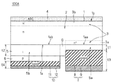
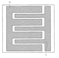
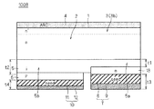
図1は、本発明の第1の実施の形態に係る太陽電池素子100Aの断面構造を示す図である。図2は、太陽電池素子100Aの裏面図である。
<First Embodiment>
<Structure of solar cell element>
FIG. 1 is a diagram showing a cross-sectional structure of solar cell element 100A according to the first embodiment of the present invention. FIG. 2 is a back view of the solar cell element 100A.

第1の実施の形態に係る太陽電池素子100Aは、第1の面1aと第2の面1bとを含み、n型(第1の導電型)のドーパント(例えばP(リン))がドープされてなることでn型の導電型を呈するn型半導体領域2を有する半導体基板1と、n型半導体領域2よりもn型のドーパント(例えばP)を高濃度に含有するドープ層3と、ノンドープのアモルファスシリコンからなるi型半導体層5と、アモルファスシリコンからなり、p型のドーパント(例えばB(ボロン))がドープされてなることでp型の導電型を呈するp型半導体層6(第2導電型層)と、n型電極7と、p型電極10と、反射防止層4とを主として備えている。   Solar cell element 100A according to the first embodiment includes first surface 1a and second surface 1b, and is doped with an n-type (first conductivity type) dopant (for example, P (phosphorus)). A semiconductor substrate 1 having an n-type semiconductor region 2 exhibiting an n-type conductivity, a doped layer 3 containing an n-type dopant (for example, P) at a higher concentration than the n-type semiconductor region 2, and a non-doped type An i-type semiconductor layer 5 made of amorphous silicon, and a p-type semiconductor layer 6 made of amorphous silicon and doped with a p-type dopant (for example, B (boron)) to exhibit a p-type conductivity type (second A conductive type layer), an n-type electrode 7, a p-type electrode 10, and an antireflection layer 4.

係る太陽電池素子100Aは、半導体基板1のn型半導体領域2とp型半導体層6とがi型半導体層5を間に挟み込んだpin接合を有する。なお、係る太陽電池素子100Aにおける表面側とは受光面側(図1においては図面視上側)を示し、裏面側とは表面の裏側の面(図1においては図面視下側)を示すものとする。   In the solar cell element 100 </ b> A, the n-type semiconductor region 2 and the p-type semiconductor layer 6 of the semiconductor substrate 1 have a pin junction with the i-type semiconductor layer 5 interposed therebetween. In addition, the surface side in the solar cell element 100A indicates the light receiving surface side (upper side in the drawing in FIG. 1), and the back side indicates the surface on the back side of the surface (the lower side in the drawing in FIG. 1). To do.

n型電極7およびp型電極10は、発電された電力を外部に取り出す電極である。図2に示すように、n型電極7およびp型電極10はいずれも、太陽電池素子100Aの裏面側に形成された、複数の電極指を有する櫛歯状電極である。裏面側において、両者の電極指は交互に並んでいる(ただし、図1においては、図示の都合上、両電極の電極指を1つずつのみ示している)。すなわち、太陽電池素子100Aは、n型電極7およびp型電極10が、太陽電池素子100Aの裏面側にのみ配されたバックコンタクト型の構造を有してなる。これにより、太陽電池素子100Aにおいては、受光面全面での受光が可能となっている。係る構成によって、変換効率の向上が図られているとともに、受光面側において電極が凸部となって存在することがないので、美観の向上も実現されている。   The n-type electrode 7 and the p-type electrode 10 are electrodes that extract the generated electric power to the outside. As shown in FIG. 2, each of the n-type electrode 7 and the p-type electrode 10 is a comb-like electrode having a plurality of electrode fingers formed on the back surface side of the solar cell element 100A. On the back side, the electrode fingers of both electrodes are alternately arranged (however, in FIG. 1, only one electrode finger of both electrodes is shown for convenience of illustration). That is, solar cell element 100A has a back contact type structure in which n-type electrode 7 and p-type electrode 10 are arranged only on the back surface side of solar cell element 100A. Thereby, in the solar cell element 100A, light can be received on the entire light receiving surface. With such a configuration, the conversion efficiency is improved, and the electrodes do not exist as convex portions on the light receiving surface side, so that the aesthetics are also improved.

半導体基板1は、例えば、n型の導電性を呈する多結晶シリコン基板である。導電型決定元素としてPを含有するn型の多結晶シリコンインゴットを鋳造法等によって形成した後、所定の大きさおよび厚みに切断することで作製される。半導体基板1の寸法例としては、大きさが10cm×10cm〜21cm×21cm程度、厚みが300μm以下であることがその好適な一例であり、さらに、厚みに関しては、200μm以下であることがより好ましい。また、半導体基板1の抵抗率は0.3〜5Ω・cm程度であるのが好ましい。     The semiconductor substrate 1 is, for example, a polycrystalline silicon substrate exhibiting n-type conductivity. An n-type polycrystalline silicon ingot containing P as a conductivity type determining element is formed by a casting method or the like, and then cut into a predetermined size and thickness. As a dimension example of the semiconductor substrate 1, a suitable example is a size of about 10 cm × 10 cm to 21 cm × 21 cm and a thickness of 300 μm or less. Further, regarding the thickness, it is more preferably 200 μm or less. . The resistivity of the semiconductor substrate 1 is preferably about 0.3 to 5 Ω · cm.

また、好ましくは、半導体基板1の表面1b側にはドープ層3の形成に先立ってあらかじめ、粗面化処理を施すことによって、微細な凹凸構造(テクスチャ構造)が形成される(図8(a)参照)。半導体基板1がこのような表面凹凸構造を有することにより、太陽電池素子100Aの受光面における光の反射損失が低減される。   Preferably, a fine concavo-convex structure (texture structure) is formed on the surface 1b side of the semiconductor substrate 1 by performing a roughening process in advance prior to the formation of the doped layer 3 (FIG. 8A). )reference). When the semiconductor substrate 1 has such a surface concavo-convex structure, the reflection loss of light on the light receiving surface of the solar cell element 100A is reduced.

ドープ層3は、半導体基板1の第1の面1aの第1領域1aaに設けられた裏面側ドープ層(第1ドープ層)3aと、半導体基板1の第2の面1bに設けられた表面側ドープ層(第2ドープ層)3bとを有する。半導体基板1の第1の面1aにおいて、ドープ層3は、pin接合が形成された領域を除いた領域に形成されている。すなわち、i型半導体層5を挟んでp型半導体層6と対向する半導体基板1の裏面の領域を除いた領域に形成される。ここで、「第2の面1bに設けられた」「第1の面1aの第1領域1aaに設けられた」とは、半導体基板1の第1(第2)の面上に形成される場合と、半導体基板1内に形成される場合とを含む。このようなドープ層3は、20nm〜5μm程度の厚みを有する。好ましくは、n型半導体領域2は、1×10¹⁵〜1×10¹⁷(cm-3)程度の濃度でn型のドーパントを含有し、ドープ層3は、1×10¹⁶〜1×10²⁰(cm-3)程度の濃度でn型のドーパントを含有する。半導体基板1にこのような態様にてドープ層3を形成することで得られる効果については、後述する。なお、半導体基板1の裏面1a側のうち、pin接合形成領域を第2領域1abとも称する。 The doped layer 3 includes a back-side doped layer (first doped layer) 3 a provided in the first region 1 aa of the first surface 1 a of the semiconductor substrate 1 and a surface provided on the second surface 1 b of the semiconductor substrate 1. And a side doped layer (second doped layer) 3b. On the first surface 1a of the semiconductor substrate 1, the doped layer 3 is formed in a region excluding the region where the pin junction is formed. That is, it is formed in a region excluding the region on the back surface of the semiconductor substrate 1 facing the p-type semiconductor layer 6 with the i-type semiconductor layer 5 interposed therebetween. Here, “provided on the second surface 1 b” and “provided on the first region 1 aa of the first surface 1 a” are formed on the first (second) surface of the semiconductor substrate 1. And a case where it is formed in the semiconductor substrate 1. Such a doped layer 3 has a thickness of about 20 nm to 5 μm. Preferably, the n-type semiconductor region 2 contains an n-type dopant at a concentration of about 1 × 10 15 to 1 × 10 17 (cm −3 ), and the doped layer 3 is 1 × 10 16 to 1 × 10 20. It contains an n-type dopant at a concentration of about (cm −3 ). The effect obtained by forming the doped layer 3 in such a manner on the semiconductor substrate 1 will be described later. Of the back surface 1a side of the semiconductor substrate 1, the pin junction formation region is also referred to as a second region 1ab.

i型半導体層5は、半導体基板1の裏面の略全面に設けられた真性半導体層である。i型半導体層5は、第1領域1aa上に設けられた部分の厚みt1が、第2領域1ab上に設けられた部分の厚みt2よりも小さい。   The i-type semiconductor layer 5 is an intrinsic semiconductor layer provided on substantially the entire back surface of the semiconductor substrate 1. In i-type semiconductor layer 5, the thickness t1 of the portion provided on first region 1aa is smaller than the thickness t2 of the portion provided on second region 1ab.

以下の説明においては、i型半導体層5のうち、第1領域1aa上に設けられた部分を第1の部分5aと称し、半導体基板1とp型半導体層6とに挟まれた領域を第2の部分5bと称する。また、本実施の形態においては、i型半導体層5のうち、第1の部分5aと第2の部分5bとの間の領域のi型半導体層5も、厚みt2で形成されているものとする。   In the following description, a portion of the i-type semiconductor layer 5 provided on the first region 1aa is referred to as a first portion 5a, and a region sandwiched between the semiconductor substrate 1 and the p-type semiconductor layer 6 is referred to as a first portion 5a. 2 part 5b. In the present embodiment, among the i-type semiconductor layers 5, the i-type semiconductor layer 5 in the region between the first portion 5a and the second portion 5b is also formed with a thickness t2. To do.

p型半導体層6は、i型半導体層5のうち、半導体基板1の裏面1aであって裏面側ドープ層3aの形成領域を除いた領域上に形成される。また、p型半導体層6は3nm〜20nm程度の厚みを有するように形成される。   The p-type semiconductor layer 6 is formed on a region of the i-type semiconductor layer 5 on the back surface 1a of the semiconductor substrate 1 excluding the formation region of the back-side doped layer 3a. The p-type semiconductor layer 6 is formed to have a thickness of about 3 nm to 20 nm.

n型電極7は、第1シード層8と第1裏面電極9とを有する。第1シード層8と第1裏面電極9とは、i型半導体層5を挟んで裏面側ドープ層3aと対向する位置に、順に形成されてなる。   The n-type electrode 7 has a first seed layer 8 and a first back electrode 9. The first seed layer 8 and the first back electrode 9 are sequentially formed at a position facing the back-side doped layer 3a with the i-type semiconductor layer 5 interposed therebetween.

p型電極10は、第2シード層11と第2裏面電極12とを有する。第2シード層11と第2裏面電極12とは、p型半導体層6の、i型半導体層5と接続していない側の面(図1の場合は下面)に、順に形成されている。   The p-type electrode 10 has a second seed layer 11 and a second back electrode 12. The second seed layer 11 and the second back electrode 12 are sequentially formed on the surface of the p-type semiconductor layer 6 that is not connected to the i-type semiconductor layer 5 (the lower surface in FIG. 1).

第1シード層8および第2シード層11は、n型電極7およびp型電極10における集電部として機能するほか、第1裏面電極9および第2裏面電極12をメッキ形成する際の下地層としての役割も果たす。第1シード層8および第2シード層11は、数百nm〜数μm程度の厚みに形成される。第1シード層8および第2シード層11は、例えば、Ni(ニッケル)、W(タングステン)、Co(コバルト)、およびこれらの合金、あるいは、Ni、W、CoとP、Bとの合金などの、導電性材料により形成される。また、ITO(酸化インジウム錫)やAg(銀)等の高反射率材料を用いて第1シード層8および第2シード層11を形成する態様であってもよい。この場合、受光面側から入射した光が第1シード層8および第2シード層11にて反射されるので、入射光の透過損失やシード層での吸収損失が低減される。   The first seed layer 8 and the second seed layer 11 function as a current collector in the n-type electrode 7 and the p-type electrode 10 and also serve as a base layer when the first back electrode 9 and the second back electrode 12 are formed by plating. Also plays a role as. The first seed layer 8 and the second seed layer 11 are formed to a thickness of about several hundred nm to several μm. The first seed layer 8 and the second seed layer 11 are, for example, Ni (nickel), W (tungsten), Co (cobalt), and alloys thereof, or alloys of Ni, W, Co, P, and B Formed of a conductive material. Alternatively, the first seed layer 8 and the second seed layer 11 may be formed using a highly reflective material such as ITO (indium tin oxide) or Ag (silver). In this case, since the light incident from the light receiving surface side is reflected by the first seed layer 8 and the second seed layer 11, transmission loss of incident light and absorption loss at the seed layer are reduced.

第1裏面電極9および第2裏面電極12は、太陽電池素子100Aにて発生した電力の外部取出電極である。第1裏面電極9および第2裏面電極12は、数μ程度の厚みに形成される。第1裏面電極および第2裏面電極12は、Cuにて形成されるが好適な一例である。あるいは、Ag、Al(アルミニウム)、Cr(クロム)、Ti(チタン)、W、Mo(モリブデン)、Ta(タンタル)、Pt(白金)、Au(金)、Ni、Coや、これらの合金など、一般的な電極材料を用いてもよい。なお、第1シード層8および第2シード層11を設けることなく、第1裏面電極9および第2裏面電極12を形成することも可能である。   The first back electrode 9 and the second back electrode 12 are external extraction electrodes for the electric power generated in the solar cell element 100A. The first back electrode 9 and the second back electrode 12 are formed to a thickness of about several μ. Although the 1st back electrode and the 2nd back electrode 12 are formed with Cu, it is a suitable example. Alternatively, Ag, Al (aluminum), Cr (chromium), Ti (titanium), W, Mo (molybdenum), Ta (tantalum), Pt (platinum), Au (gold), Ni, Co, and alloys thereof A general electrode material may be used. Note that the first back electrode 9 and the second back electrode 12 can be formed without providing the first seed layer 8 and the second seed layer 11.

なお、太陽電池素子100Aの発電効率を向上させるうえでは、図2のように太陽電池素子100Aを裏面側から見たときのp型電極10の平面占有面積が、n型電極7の平面占有面積よりも大きくなるように、n型電極7とp型電極10とを形成するのが好適である。この場合、裏面側ドープ層3aも、n型電極7の形成範囲に対応する領域にのみ形成するようにする。例えば、n型電極7とp型電極10との平面占有面積の比が1:9〜4:6の範囲に形成するのが好ましく、特に、3:7程度とするのが好ましい。   In order to improve the power generation efficiency of the solar cell element 100A, the plane occupation area of the p-type electrode 10 when the solar cell element 100A is viewed from the back side as shown in FIG. It is preferable to form the n-type electrode 7 and the p-type electrode 10 so as to be larger. In this case, the back-side doped layer 3 a is also formed only in a region corresponding to the formation range of the n-type electrode 7. For example, it is preferable that the ratio of the plane occupation area between the n-type electrode 7 and the p-type electrode 10 is in the range of 1: 9 to 4: 6, particularly about 3: 7.

さらに、n型電極7およびp型電極10は、両者の電気抵抗値が等しくなるように、各々の厚みが定められるのが好ましい。図1に示すように、n型電極7の厚みt3は、第1シード層8の厚みと第1裏面電極9の厚みとの総和であり、p型電極10の厚みt4は、第2シード層11の厚みと第2裏面電極12の厚みとの総和である。例えば、上述のように、n型電極7とp型電極10との平面占有面積の比を3:7としたときは、t3:t4=7:3程度とするのがよい。   Furthermore, it is preferable that the thicknesses of the n-type electrode 7 and the p-type electrode 10 are determined so that the electric resistance values of both are equal. As shown in FIG. 1, the thickness t3 of the n-type electrode 7 is the sum of the thickness of the first seed layer 8 and the thickness of the first back electrode 9, and the thickness t4 of the p-type electrode 10 is the second seed layer. 11 and the thickness of the second back electrode 12. For example, as described above, when the ratio of the plane occupation area between the n-type electrode 7 and the p-type electrode 10 is set to 3: 7, t3: t4 = 7: 3 is preferable.

反射防止層4は、受光面側から太陽電池素子100Aに入射する光の反射損失の低減を目的として設けられる層である。また、反射防止層4は、半導体基板1の保護層としての役割も有する。反射防止層4は、表面側ドープ層3bを被覆するように形成されている。このように反射防止層4を形成することで、半導体基板1へのバルクおよび表面へのパッシベーション効果が増大し、開放電圧や短絡電流密度が向上するという効果が得られる。   The antireflection layer 4 is a layer provided for the purpose of reducing the reflection loss of light incident on the solar cell element 100A from the light receiving surface side. The antireflection layer 4 also serves as a protective layer for the semiconductor substrate 1. The antireflection layer 4 is formed so as to cover the surface side doped layer 3b. By forming the antireflection layer 4 in this way, the effect of passivation to the bulk and the surface of the semiconductor substrate 1 is increased, and the effect of improving the open circuit voltage and the short circuit current density can be obtained.

反射防止層4の構成材料や厚みは、半導体基板1との屈折率の差などを考慮して定められる。反射防止層4は、屈折率2程度の材料であるSiO2(酸化シリコン)、SiN(窒化シリコン)、TiO2(酸化チタン)、あるいはMgF2(フッ化マグネシウム)等により、厚みが50〜200nm程度となるように、形成されるのがその好適な一例である。 The constituent material and thickness of the antireflection layer 4 are determined in consideration of the difference in refractive index from the semiconductor substrate 1. The antireflection layer 4 is made of SiO 2 (silicon oxide), SiN (silicon nitride), TiO 2 (titanium oxide), MgF 2 (magnesium fluoride) or the like, which is a material having a refractive index of about 2 , and has a thickness of 50 to 200 nm. It is a preferable example that it is formed so as to have a degree.

<ドープ層形成の効果>
次に、太陽電池素子100Aに上述のような形態にてドープ層3を設けることで得られる効果について説明する。
<Effect of dope layer formation>
Next, an effect obtained by providing the solar cell element 100A with the doped layer 3 in the above-described form will be described.

まず、ドープ層3のうち、表面側ドープ層3bは、半導体基板1の表面側の界面付近におけるキャリアの再結合損失を低減する効果(表面電界効果)を有する、FSF層(表面電界層)として機能する。一方、裏面側ドープ層3aは、半導体基板1の裏面側の界面付近におけるキャリアの再結合損失を低減する効果(裏面電界効果)を有する、BSF層(裏面電界層)として機能する。すなわち、半導体基板1の両面にドープ層3を備えることは、太陽電池素子100Aにおける発電効率を向上させる効果を有する。   First, in the doped layer 3, the surface-side doped layer 3 b is an FSF layer (surface electric field layer) having an effect of reducing the recombination loss of carriers in the vicinity of the interface on the surface side of the semiconductor substrate 1 (surface electric field effect). Function. On the other hand, the back-side doped layer 3 a functions as a BSF layer (back-side field layer) having an effect of reducing carrier recombination loss in the vicinity of the back-side interface of the semiconductor substrate 1 (back-side field effect). That is, providing the doped layer 3 on both surfaces of the semiconductor substrate 1 has an effect of improving the power generation efficiency in the solar cell element 100A.

好ましくは、ドープ層3は、P等のn型ドーパント原子が存在する雰囲気下で半導体基板1を900℃程度の温度に加熱し、該n型ドーパント原子を半導体基板1の内部に拡散させる熱拡散法によって形成される熱拡散層である(詳細は後述)。係る加熱の際には、半導体基板1中に(n型半導体領域2中に)含まれている金属不純物(例えば、Fe、Cu、Alなど)がドープ層3側へと拡散して移動し、n型半導体領域2におけるこれら金属不純物の濃度が低減する、金属ゲッタリング効果が得られる。これにより、n型半導体領域2内における不純物原子の存在に起因したキャリアの再結合が低減されるので、太陽電池素子における発電効率がさらに向上する。   Preferably, the doped layer 3 is a thermal diffusion that heats the semiconductor substrate 1 to a temperature of about 900 ° C. in an atmosphere in which an n-type dopant atom such as P exists, and diffuses the n-type dopant atom into the semiconductor substrate 1. It is a thermal diffusion layer formed by the method (details will be described later). During such heating, metal impurities (for example, Fe, Cu, Al, etc.) contained in the semiconductor substrate 1 (in the n-type semiconductor region 2) diffuse and move to the doped layer 3 side, A metal gettering effect is obtained in which the concentration of these metal impurities in the n-type semiconductor region 2 is reduced. Thereby, since carrier recombination due to the presence of impurity atoms in n-type semiconductor region 2 is reduced, power generation efficiency in the solar cell element is further improved.

特に、ホールに対して比較的大きな捕獲断面積を有するFe不純物が低減することは、多結晶シリコンからなる半導体基板1のライフタイムを向上させる効果もある。なお、FSF層やBSF層としての機能を持たせることが目的であれば、上述のように熱拡散層として形成する態様に代えて、半導体基板1の表面にアモルファスシリコンからなるドープ層3を積層形成する態様であってもよい。   In particular, the reduction of Fe impurities having a relatively large capture cross section with respect to holes also has the effect of improving the lifetime of the semiconductor substrate 1 made of polycrystalline silicon. If the purpose is to provide a function as an FSF layer or a BSF layer, the doped layer 3 made of amorphous silicon is laminated on the surface of the semiconductor substrate 1 instead of the embodiment of forming as a thermal diffusion layer as described above. The form to form may be sufficient.

n型半導体領域2における不純物濃度が低減されれば、n型半導体領域2内における不純物原子の存在に起因したキャリアの再結合が低減されるので、上述のようにドープ層3を形成してなる太陽電池素子100Aは、品質を改善させて発電効率を向上させたものであるといえる。   If the impurity concentration in the n-type semiconductor region 2 is reduced, carrier recombination due to the presence of impurity atoms in the n-type semiconductor region 2 is reduced, so that the doped layer 3 is formed as described above. It can be said that the solar cell element 100A has improved quality and improved power generation efficiency.

一方で、ドープ層3は、太陽電池素子100Aのpin接合が形成された第2領域1abに形成されていない。これにより、太陽電池素子100Aにおいては、pin接合界面における欠陥密度は低く保たれており、該界面におけるキャリアの再結合損失は低減されてなる。   On the other hand, the doped layer 3 is not formed in the second region 1ab where the pin junction of the solar cell element 100A is formed. Thereby, in solar cell element 100A, the defect density at the pin junction interface is kept low, and the recombination loss of carriers at the interface is reduced.

<i型半導体層の厚みと発電効率との関係>
次に、i型半導体層5の厚み(i型半導体層5の第1の部分5aの厚みt1および第2の部分5bの厚みt2)と、素子の発電効率との関係について説明する。
<Relationship between thickness of i-type semiconductor layer and power generation efficiency>
Next, the relationship between the thickness of the i-type semiconductor layer 5 (the thickness t1 of the first portion 5a and the thickness t2 of the second portion 5b of the i-type semiconductor layer 5) and the power generation efficiency of the element will be described.

本実施の形態に係る太陽電池素子100Aでは、n型半導体領域2とp型半導体層6との間にi型半導体層5が形成されている。このi型半導体層5の存在によって、n型半導体領域2とp型半導体層6との間の領域におけるキャリアの再結合損失が低減されている。   In solar cell element 100 </ b> A according to the present embodiment, i-type semiconductor layer 5 is formed between n-type semiconductor region 2 and p-type semiconductor layer 6. Due to the presence of the i-type semiconductor layer 5, carrier recombination loss in the region between the n-type semiconductor region 2 and the p-type semiconductor layer 6 is reduced.

一般に、n型半導体層とp型半導体層とが直接に接合されたpn接合を備える太陽電池素子においては、n型半導体層とp型半導体層との固有の欠陥に起因して、接合界面に多数の界面準位が存在するため、空乏層領域におけるキャリアの再結合損失が増大し、素子発電効率の低下を招く。   Generally, in a solar cell element having a pn junction in which an n-type semiconductor layer and a p-type semiconductor layer are directly joined, due to an inherent defect between the n-type semiconductor layer and the p-type semiconductor layer, the junction interface Since there are a large number of interface states, the carrier recombination loss in the depletion layer region increases, leading to a reduction in device power generation efficiency.

これに対して、太陽電池素子100Aのように、n型半導体層とp型半導体層との間にi型半導体層を挟んでpin接合を形成した太陽電池素子においては、pn接合を有する太陽電池素子と比較して、より階段型接合に近似した接合が形成され、空乏層領域における欠陥密度が小さくなるので、キャリアの再結合は低減される。   On the other hand, in a solar cell element in which a pin junction is formed by sandwiching an i-type semiconductor layer between an n-type semiconductor layer and a p-type semiconductor layer as in the solar cell element 100A, a solar cell having a pn junction. Compared with the device, a junction closer to a step-type junction is formed, and the defect density in the depletion layer region is reduced, so that carrier recombination is reduced.

また、太陽電池素子100Aの場合、裏面側ドープ層3aと第1シード層8との間にもi型半導体層5が形成されている。これにより、欠陥密度が大きい裏面側ドープ層3aと第1シード層8とが直接、接する場合よりも、キャリアの再結合損失が低減される。   In the case of the solar cell element 100 </ b> A, the i-type semiconductor layer 5 is also formed between the back-side doped layer 3 a and the first seed layer 8. Thereby, the recombination loss of carriers is reduced as compared with the case where the back-side doped layer 3a having a high defect density and the first seed layer 8 are in direct contact with each other.

これらのキャリアの再結合損失の低減効果は、i型半導体層5の厚みが大きいほど顕著となる。   The effect of reducing the recombination loss of these carriers becomes more significant as the thickness of the i-type semiconductor layer 5 increases.

一方、太陽電池素子100Aにおいては、i型半導体5の第1の部分5aをトンネリングした多数キャリアがn型電極7へ達し、i型半導体5の第2の部分5bをトンネリングした少数キャリアがp型電極10に達することによって、電流が流れる。よって、キャリアのトンネリング確率が大きいほど、太陽電池素子100Aの発電効率は向上することになる。i型半導体層5が薄いほどキャリアのトンネリング確率は増大するので、i型半導体層5を厚くすることは、キャリアのトンネリング確率を低下させ、発電効率を低下させることにつながる。   On the other hand, in solar cell element 100A, the majority carriers that tunnel first portion 5a of i-type semiconductor 5 reach n-type electrode 7, and the minority carriers that tunnel second portion 5b of i-type semiconductor 5 are p-type. By reaching the electrode 10, a current flows. Therefore, the higher the carrier tunneling probability, the higher the power generation efficiency of the solar cell element 100A. As the i-type semiconductor layer 5 is thinner, the carrier tunneling probability increases. Therefore, increasing the thickness of the i-type semiconductor layer 5 lowers the carrier tunneling probability and lowers the power generation efficiency.

従って、発電効率の向上に最適なi型半導体層5の厚みは、これを大きくすることによるキャリアの再結合低減効果と、小さくすることによるトンネリング確率増大の効果とのバランスで定まることになる。   Therefore, the optimal thickness of the i-type semiconductor layer 5 for improving the power generation efficiency is determined by the balance between the effect of reducing carrier recombination by increasing the thickness and the effect of increasing the tunneling probability by decreasing the thickness.

ここで、太陽電池素子100Aの場合、裏面側ドープ層3aのフェルミ準位とn型電極7の仕事関数の差は、p型半導体層6とn型半導体領域2とのフェルミ準位の差と比較して非常に小さい。従って、i型半導体領域の第1の部分5aの方が、第2の部分5bよりも、トンネリング確率を確保するために薄くすることの必要性が大きいといえる。   Here, in the case of the solar cell element 100A, the difference between the Fermi level of the back-side doped layer 3a and the work function of the n-type electrode 7 is the difference between the Fermi level of the p-type semiconductor layer 6 and the n-type semiconductor region 2. Very small compared. Therefore, it can be said that the first part 5a of the i-type semiconductor region is more required to be thinner than the second part 5b in order to ensure the tunneling probability.

そこで、太陽電池素子100Aにおいては、i型半導体層5を均一な厚みで形成するのではなく、i型半導体5の第1の部分5aの厚みt1が第2の部分5bの厚みt2よりも小さくなるように、i型半導体層5を形成している。   Therefore, in the solar cell element 100A, the i-type semiconductor layer 5 is not formed with a uniform thickness, but the thickness t1 of the first portion 5a of the i-type semiconductor 5 is smaller than the thickness t2 of the second portion 5b. Thus, the i-type semiconductor layer 5 is formed.

具体的には、厚みt1が3nm以上5nm以下であり、厚みt2が6nm以上10nm以下である場合に、高い発電効率が得られる。係る範囲は、厚みt1および厚みt2を(t1≧t2の場合も含めて)種々の値に設定した太陽電池素子について発電効率を求めることにより定められる。   Specifically, high power generation efficiency is obtained when the thickness t1 is 3 nm or more and 5 nm or less and the thickness t2 is 6 nm or more and 10 nm or less. Such a range is determined by determining the power generation efficiency for solar cell elements in which the thickness t1 and the thickness t2 are set to various values (including the case where t1 ≧ t2).

厚みt1が3nm以下であれば、裏面側ドープ層3a下面の界面準位密度の増大により開放電圧が減少し、5nm以上であれば電子のトンネリング確率の減少により曲線因子(Fill Factor)が小さくなる。また、厚みt2が6nm以下であれば、pn接合部での欠陥密度の増大により開放電圧が減少し、10nm以上であれば少数キャリアのトンネリング確率の減少により曲線因子が小さくなる。   If the thickness t1 is 3 nm or less, the open circuit voltage decreases due to an increase in the interface state density on the lower surface of the back-side doped layer 3a. If the thickness t1 is 5 nm or more, the fill factor decreases due to a decrease in the electron tunneling probability. . If the thickness t2 is 6 nm or less, the open circuit voltage decreases due to an increase in the defect density at the pn junction, and if it is 10 nm or more, the curve factor decreases due to a decrease in the minority carrier tunneling probability.

なお、さらに曲線因子を向上させる目的で、i型半導体5の第1の部分5aにコンタクトホールを形成してもよい。ただし、裏面側ドープ層3aと第1シード層8との界面での再結合損失を極力低減するため、コンタクトホールの形成領域はi型半導体5の第1の部分5aの面積の1%以下に抑えることが好ましい。   Note that a contact hole may be formed in the first portion 5a of the i-type semiconductor 5 for the purpose of further improving the fill factor. However, in order to reduce the recombination loss at the interface between the back-side doped layer 3a and the first seed layer 8 as much as possible, the contact hole formation region is 1% or less of the area of the first portion 5a of the i-type semiconductor 5. It is preferable to suppress.

以上、説明したように、本実施の形態によれば、i型半導体5の第1の部分5aと第2の部分5bの厚みを最適化しているので、高い発電効率を有する太陽電池素子を得ることができる。   As described above, according to the present embodiment, since the thickness of the first portion 5a and the second portion 5b of the i-type semiconductor 5 is optimized, a solar cell element having high power generation efficiency is obtained. be able to.

<太陽電池素子の製造方法>
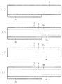
次に、第1の実施の形態に係る太陽電池素子100Aの製造方法について説明する。以降の説明においては、n型のドーパントとしてPが用いられ、半導体基板が表面凹凸構造を有する太陽電池素子100Aを製造する場合を例として説明する。図3は、太陽電池素子100Aの製造工程の流れを示す図である。図4ないし図6は、製造工程の途中段階における素子の構造を模式的に示す図である。
<Method for producing solar cell element>
Next, a method for manufacturing the solar cell element 100A according to the first embodiment will be described. In the following description, a case where P is used as an n-type dopant and the semiconductor substrate has a surface uneven structure will be described as an example. FIG. 3 is a diagram showing a flow of manufacturing steps of the solar cell element 100A. 4 to 6 are diagrams schematically showing the structure of the element in the middle of the manufacturing process.

まず、P等のn型ドーパント原子を所定の濃度で含有するn型の多結晶シリコンインゴットが、鋳造法等により形成され、所定の大きさおよび厚みに切断されることによって、n型の多結晶シリコン基板(半導体基板1)が得られる(ステップS1)。得られた半導体基板1のスライス面を清浄化するために、NaOH(水酸化ナトリウム)やKOH(水酸化カリウム)等のアルカリ溶液、フッ酸、あるいはフッ酸と硝酸との混合溶液等でごくわずかにエッチングする。   First, an n-type polycrystalline silicon ingot containing an n-type dopant atom such as P at a predetermined concentration is formed by a casting method or the like and cut into a predetermined size and thickness, whereby an n-type polycrystalline is obtained. A silicon substrate (semiconductor substrate 1) is obtained (step S1). In order to clean the sliced surface of the obtained semiconductor substrate 1, it is very slight with an alkaline solution such as NaOH (sodium hydroxide) or KOH (potassium hydroxide), hydrofluoric acid, or a mixed solution of hydrofluoric acid and nitric acid. Etch into.

続いて、半導体基板1の表面(すなわち受光面側となる面)を、ドライエッチングや、ウェットエッチングによって粗面化することで、該半導体基板1の表面に、光反射率の低減機能を有する凹凸構造を形成する。   Subsequently, the surface of the semiconductor substrate 1 (that is, the surface on the light receiving surface side) is roughened by dry etching or wet etching, so that the surface of the semiconductor substrate 1 has unevenness having a function of reducing light reflectance. Form a structure.

反応性イオンエッチングにより表面凹凸構造を形成した後には、例えば、超音波洗浄などの手法によって半導体基板1の表面(凹凸構造形成面)に残ったエッチング残渣の除去を行う。   After the surface concavo-convex structure is formed by reactive ion etching, the etching residue remaining on the surface of the semiconductor substrate 1 (uneven structure forming surface) is removed by a technique such as ultrasonic cleaning.

次に、図4(a)に示すように、半導体基板1の裏面側において、裏面側3aの形成が予定される領域を除いた領域に、マスク20を形成する(ステップS2)。つまり、半導体基板1の裏面においてpin接合の形成が予定される領域(第2領域)は、少なくともマスク20によって被覆されることになる。マスク20は、液体材料の塗布および焼成などによるいわゆる塗布法によって厚膜として形成する態様であってもよいし、CVD法やスパッタリング法の薄膜形成手法によって薄膜として形成する態様であってもよい。   Next, as shown in FIG. 4A, a mask 20 is formed on the back side of the semiconductor substrate 1 in a region excluding the region where the back side 3a is scheduled to be formed (step S2). That is, a region (second region) where a pin junction is to be formed on the back surface of the semiconductor substrate 1 is covered with at least the mask 20. The mask 20 may be formed as a thick film by a so-called application method such as application and baking of a liquid material, or may be formed as a thin film by a thin film formation method such as a CVD method or a sputtering method.

続いて、図4(b)に示すように、ドープ層3を形成する(ステップS3)。ドープ層3の形成には、マスク20の形成後の半導体基板1の表面および裏面全面にペースト状のP25(五酸化二リン)を塗布して熱拡散させる塗布熱拡散方法を用いることができる。あるいは、半導体基板1の側面についてもマスク20を形成したうえで、ガス状態にしたPOCl3(オキシ塩化リン)を拡散源として熱拡散させる気相熱拡散方法や、P+イオンを直接拡散させるイオン打ち込み法等の方法を用いる態様であってもよい。これらの手法においては、半導体基板1を500℃〜950℃程度に加熱する。このような処理により、マスク20の形成領域を除いて、半導体基板1の表面および裏面にドープ層3が形成される。なお、ドープ層3は、半導体基板1の側面にも形成される態様であってもよい。 Subsequently, as shown in FIG. 4B, a doped layer 3 is formed (step S3). For the formation of the doped layer 3, a coating thermal diffusion method is used in which paste-like P 2 O 5 (diphosphorus pentoxide) is applied to the entire front and back surfaces of the semiconductor substrate 1 after the mask 20 is formed and thermally diffused. Can do. Alternatively, the mask 20 is formed also on the side surface of the semiconductor substrate 1, and a gas phase thermal diffusion method in which POCl 3 (phosphorus oxychloride) in a gas state is thermally diffused as a diffusion source or ions that directly diffuse P + ions are used. A mode using a method such as a driving method may be used. In these methods, the semiconductor substrate 1 is heated to about 500 ° C. to 950 ° C. By such treatment, the doped layer 3 is formed on the front surface and the back surface of the semiconductor substrate 1 except for the formation region of the mask 20. The doped layer 3 may also be formed on the side surface of the semiconductor substrate 1.

マスク20は、ドープ層3の形成後にフッ酸等でエッチング除去される。図4(c)には、ドープ層3を形成し、マスク20を除去した後の半導体基板1を示している。   The mask 20 is removed by etching with hydrofluoric acid after the doped layer 3 is formed. FIG. 4C shows the semiconductor substrate 1 after the doped layer 3 is formed and the mask 20 is removed.

なお、マスク20を用いる代わりに、いったん半導体基板1の全面に熱拡散法により高濃度のn型ドープ層を形成し、その後、ドープ層3として残存させる必要のない部分をエッチング除去するといった方法を用いてもよい。具体的には、高濃度のn型ドープ層を半導体基板1の全面に形成した後、該ドープ層をドープ層3として残存させる領域にレジストを塗布したうえで、フッ酸あるいはフッ酸と硝酸との混合液を用いてエッチングを行い、最後にレジスト膜を除去すればよい。係る場合においては、エッチングは、レーザスクライブ処理やサンドブラスト処理などの手法で行ってもよい。   Instead of using the mask 20, a method of once forming a high-concentration n-type doped layer on the entire surface of the semiconductor substrate 1 by a thermal diffusion method and then etching away a portion that does not need to remain as the doped layer 3 is performed. It may be used. Specifically, after a high-concentration n-type doped layer is formed on the entire surface of the semiconductor substrate 1, a resist is applied to a region where the doped layer is left as the doped layer 3, and then hydrofluoric acid or hydrofluoric acid and nitric acid are used. Etching is performed using the mixed solution, and the resist film is finally removed. In such a case, the etching may be performed by a technique such as laser scribing or sand blasting.

また、ドープ層3の表層のドーパント濃度が高い場合には、フッ酸と硝酸との混合溶液等でエッチングして、ドーピングプロファイルを制御することが好ましい。   When the dopant concentration of the surface layer of the doped layer 3 is high, it is preferable to control the doping profile by etching with a mixed solution of hydrofluoric acid and nitric acid.

続いて、ドープ層3が形成された半導体基板1を洗浄する(ステップS4)。半導体基板1の洗浄は、RCA洗浄、SPM洗浄、水素水洗浄、およびオゾン水洗浄等のウェット洗浄や、アッシングやUV洗浄等のドライ洗浄によって行う。また、酸化膜を除去するために、半導体基板1をフッ酸やNH4F(フッ化アンモニウム)溶液等に浸漬し、その後水洗する。 Subsequently, the semiconductor substrate 1 on which the doped layer 3 is formed is cleaned (step S4). The semiconductor substrate 1 is cleaned by wet cleaning such as RCA cleaning, SPM cleaning, hydrogen water cleaning and ozone water cleaning, or dry cleaning such as ashing and UV cleaning. Further, in order to remove the oxide film, the semiconductor substrate 1 is immersed in hydrofluoric acid or NH 4 F (ammonium fluoride) solution, and then washed with water.

上述の洗浄後、図4(d)および図5(a)に示すように、i型半導体層5を形成する(ステップS5、S6)。まず、図4(d)に示すように、半導体基板1の裏面においてpin接合の形成予定領域(第2領域)に、i型のアモルファスシリコン膜21を形成する(ステップS5)。i型のアモルファスシリコン膜21の形成には、PECVD法、光CVD法、CatCVD法、蒸着法、またはスパッタ法等を用いることができる。PECVD法を用いる場合であれば、水素とシランとを原料ガスとし、PECVD装置のチャンバ内のガス圧を0.1〜5Torr、基板温度を100〜200℃という成長条件で形成するのが好適な一例である。なお、半導体基板1裏面の所望の領域にのみアモルファスシリコン膜21を形成するには、CVD法による成膜時にメタルマスク等で非成膜領域をマスクするか、あるいは、フォトリソグラフィー法等を用いればよい。   After the above cleaning, as shown in FIGS. 4D and 5A, the i-type semiconductor layer 5 is formed (steps S5 and S6). First, as shown in FIG. 4D, an i-type amorphous silicon film 21 is formed in a region (second region) where a pin junction is to be formed on the back surface of the semiconductor substrate 1 (step S5). For the formation of the i-type amorphous silicon film 21, a PECVD method, a photo CVD method, a CatCVD method, a vapor deposition method, a sputtering method, or the like can be used. In the case of using the PECVD method, it is preferable that hydrogen and silane are used as source gases, the gas pressure in the chamber of the PECVD apparatus is 0.1 to 5 Torr, and the substrate temperature is 100 to 200 ° C. It is an example. In order to form the amorphous silicon film 21 only in a desired region on the back surface of the semiconductor substrate 1, a non-deposition region is masked with a metal mask or the like at the time of film formation by the CVD method, or a photolithography method or the like is used. Good.

続いて、図5(a)に示すように、半導体基板1の裏面側全体に、i型のアモルファスシリコン膜22を形成する(ステップS6)。具体的には、半導体基板1の裏面側において、アモルファスシリコン膜21が形成されている領域においてはその下側に、形成されていない領域においては半導体基板1の裏面に直接に、アモルファスシリコン膜22が形成される。該アモルファスシリコン膜22を形成には、ステップS5と同様の手法が用いられる。   Subsequently, as shown in FIG. 5A, an i-type amorphous silicon film 22 is formed on the entire back surface of the semiconductor substrate 1 (step S6). Specifically, on the back surface side of the semiconductor substrate 1, the amorphous silicon film 22 is directly below the back surface of the semiconductor substrate 1 in the region where the amorphous silicon film 21 is formed, and in the region where the amorphous silicon film 21 is not formed. Is formed. For the formation of the amorphous silicon film 22, the same technique as in step S5 is used.

ステップS5およびステップS6の工程を経て、アモルファスシリコン膜21および22からなるより厚みの大きい領域と、アモルファスシリコン膜22のみからなるより厚みの小さい領域と、を有するi型半導体層5が形成される。   Through steps S5 and S6, i-type semiconductor layer 5 having a thicker region made of amorphous silicon films 21 and 22 and a thinner region made only of amorphous silicon film 22 is formed. .

i型半導体層5において、i型半導体5の第1の部分5aは、アモルファスシリコン膜21のみからなる領域の所定部分(第1領域に隣接形成されてなる部分)であり、その厚みt1はアモルファスシリコン膜21の膜厚と等しくなる。また、i型半導体5の第2の部分5bは、アモルファスシリコン膜21およびアモルファスシリコン膜22により形成される領域であり、その厚みt2は、アモルファスシリコン膜21および22の厚みの総和となる。両領域の厚みt1および厚みt2を所望の厚みとするには、i型アモルファスシリコン膜21および22の膜厚を調整して、i型半導体層5を形成すればよい。   In the i-type semiconductor layer 5, the first portion 5a of the i-type semiconductor 5 is a predetermined portion (a portion formed adjacent to the first region) of a region made only of the amorphous silicon film 21, and its thickness t1 is amorphous. It becomes equal to the film thickness of the silicon film 21. The second portion 5b of the i-type semiconductor 5 is a region formed by the amorphous silicon film 21 and the amorphous silicon film 22, and the thickness t2 is the sum of the thicknesses of the amorphous silicon films 21 and 22. In order to obtain the desired thickness t1 and thickness t2 in both regions, the i-type semiconductor layer 5 may be formed by adjusting the film thicknesses of the i-type amorphous silicon films 21 and 22.

なお、i型半導体層5の形成には、ステップS5およびステップS6における処理に代わり、以下の方法を用いてもよい。まず、半導体基板1の裏面全面にi型のアモルファスシリコン膜を所望の厚みで形成する。続いて、該アモルファスシリコン膜を介して第2領域(pin接合形成領域)と対向する領域に、さらにi型のアモルファスシリコン膜を所望の厚みで形成し、i型半導体層5を形成する態様であってもよい。この場合においても、i型半導体5の第1の部分5aおよび第2の部分5bを所望の厚みで形成することが可能である。   Note that the following method may be used for forming the i-type semiconductor layer 5 instead of the processing in step S5 and step S6. First, an i-type amorphous silicon film is formed on the entire back surface of the semiconductor substrate 1 with a desired thickness. Subsequently, an i-type semiconductor layer 5 is formed by forming an i-type amorphous silicon film with a desired thickness in a region facing the second region (pin junction formation region) through the amorphous silicon film. There may be. Even in this case, the first portion 5a and the second portion 5b of the i-type semiconductor 5 can be formed with a desired thickness.

i型半導体層5が形成されると、図5(b)に示すように、p型半導体層6を形成する(ステップS7)。p型半導体層6は、非形成領域(i型半導体5の第2の部分5bを挟んで、半導体基板1と対向する領域を除いた領域)にマスクを行ったうえで、i型半導体層5の表面に、3〜20nmの厚みに形成する。PECVD法を用いる場合であれば、水素とシランとジボランとを原料ガスとし、PECVD装置のチャンバ内のガス圧を0.1〜5Torr、基板温度を100〜200℃という成長条件でBがドープされたアモルファスシリコン層を形成するのが好適な一例である。あるいは、フォトリソグラフィー法等によって非形成領域以外にp型半導体層6を形成するようにしてもよい。   When the i-type semiconductor layer 5 is formed, the p-type semiconductor layer 6 is formed as shown in FIG. 5B (step S7). The p-type semiconductor layer 6 is formed by masking a non-formation region (a region excluding a region facing the semiconductor substrate 1 with the second portion 5b of the i-type semiconductor 5 in between), and then the i-type semiconductor layer 5 Is formed to a thickness of 3 to 20 nm. In the case of using the PECVD method, hydrogen, silane, and diborane are used as source gases, B is doped under growth conditions of a gas pressure in a chamber of the PECVD apparatus of 0.1 to 5 Torr, and a substrate temperature of 100 to 200 ° C. A preferred example is to form an amorphous silicon layer. Alternatively, the p-type semiconductor layer 6 may be formed in a region other than the non-formation region by a photolithography method or the like.

次に、図5(c)に示すように、反射防止層4を形成する(ステップS8)。反射防止層4の形成は、PECVD法、CatCVD法、スパッタリング法、蒸着法等により行うことができる。   Next, as shown in FIG. 5C, the antireflection layer 4 is formed (step S8). The antireflection layer 4 can be formed by PECVD, CatCVD, sputtering, vapor deposition, or the like.

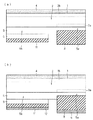
次に、図6(a)に示すように、第1シード層8および第2シード層11を形成する(ステップS9)。第1シード層8および第2シード層11は、Ni、W、Coおよびこれらの合金や、Ni、W、CoとP、Bとの合金などによって形成される。第1シード層8および第2シード層11は、無電解メッキによって形成することができる。この場合、薬液温度を150℃以下とし、厚さが1μm以下となるように形成するのが好ましい。第1シード層8および第2シード層11は、後に第1裏面電極9および第2裏面電極12を形成する際の下地層としての機能することになる。   Next, as shown in FIG. 6A, the first seed layer 8 and the second seed layer 11 are formed (step S9). The first seed layer 8 and the second seed layer 11 are made of Ni, W, Co, and alloys thereof, or alloys of Ni, W, Co, P, and B. The first seed layer 8 and the second seed layer 11 can be formed by electroless plating. In this case, it is preferable to form the chemical solution at a temperature of 150 ° C. or less and a thickness of 1 μm or less. The first seed layer 8 and the second seed layer 11 function as a base layer when the first back electrode 9 and the second back electrode 12 are formed later.

なお、n型電極7を構成する第1シード層8とp型電極10を構成する第2シード層11とは、両者が連続しないように(互いに絶縁されるように)形成する必要がある。これは、それぞれを形成するための無電解メッキを行うに際して、その形成対象領域(第1シード層8の場合はi型半導体層5の表面、第2シード層11の場合はp型半導体層6の表面)のみを選択的に活性化させるようにすることで実現される。あるいは、第1シード層8および第2シード層11を構成することになる金属層を無電解メッキによって半導体基板1の裏面側全体に形成した後に、レーザを用いて不要部分を除去するようにしてもよい。なお、レーザによる除去に代わり、不要部分以外をレジスト膜等で被覆し、当該不要部分をエッチング除去する方法を用いることもできる。この場合、エッチング除去後にレジスト膜をウェットエッチング等によって除去し、さらに、有機残存成分をUV洗浄等によって除去する処理を行うようにする。   The first seed layer 8 constituting the n-type electrode 7 and the second seed layer 11 constituting the p-type electrode 10 need to be formed so that they are not continuous (insulated from each other). This is because, when performing electroless plating to form each, the formation target region (the surface of the i-type semiconductor layer 5 in the case of the first seed layer 8 and the p-type semiconductor layer 6 in the case of the second seed layer 11). This is realized by selectively activating only the surface. Alternatively, after forming a metal layer constituting the first seed layer 8 and the second seed layer 11 on the entire back side of the semiconductor substrate 1 by electroless plating, unnecessary portions are removed using a laser. Also good. Instead of removing by laser, a method of covering other than unnecessary portions with a resist film or the like and etching away the unnecessary portions can be used. In this case, after the etching removal, the resist film is removed by wet etching or the like, and further, a process of removing organic residual components by UV cleaning or the like is performed.

最後に、図6(b)に示すように、第1裏面電極9および第2裏面電極12を形成する(ステップS10)。第1裏面電極9および第2裏面電極12としては、電解メッキによりCuを形成材料として形成するのが好適である。なお、無電解メッキを行った後には、接着強度向上のため50〜350℃の温度で乾燥処理を行う。   Finally, as shown in FIG. 6B, the first back electrode 9 and the second back electrode 12 are formed (step S10). The first back electrode 9 and the second back electrode 12 are preferably formed by using Cu as a forming material by electrolytic plating. In addition, after performing electroless plating, a drying process is performed at the temperature of 50-350 degreeC for the adhesive strength improvement.

なお、第1裏面電極9および第2裏面電極12の形成は、無電解メッキによる他、光メッキ、スクリーン印刷、ドクターブレード法、あるいはディスペンサー塗布法などの種々の塗布法によって導電性ペーストを塗布してこれを焼成する方法や、スパッタリング法や蒸着法などの種々の真空成膜手法を用いることもできる。裏面電極の形成材料としては、製法に合わせて、Ag、Al、Cr、Ti、W、Mo、Ta、Pt、Au、Ni、Coおよびこれらの合金を用いることができる。   The first back electrode 9 and the second back electrode 12 are formed by applying a conductive paste by various coating methods such as photoplating, screen printing, doctor blade method, or dispenser coating method, in addition to electroless plating. In addition, various vacuum film forming methods such as a method of firing this, a sputtering method, a vapor deposition method, and the like can be used. As a material for forming the back electrode, Ag, Al, Cr, Ti, W, Mo, Ta, Pt, Au, Ni, Co and alloys thereof can be used according to the manufacturing method.

以上の工程を経ることで、第1の実施の形態に係る太陽電池素子100Aが完成する。   Through the above steps, the solar cell element 100A according to the first embodiment is completed.

<第2の実施の形態>
次に、第2の実施の形態に係る太陽電池素子100Bについて説明する。図7は、第2の実施の形態に係る太陽電池素子100Bの断面構造を示す図である。なお、第1の実施の形態に係る太陽電池素子100Aと同様の作用効果を奏する構成要素については、同一の符号を付し、以下ではその説明を省略する。
<Second Embodiment>
Next, a solar cell element 100B according to the second embodiment will be described. FIG. 7 is a diagram showing a cross-sectional structure of solar cell element 100B according to the second embodiment. In addition, about the component which show | plays the effect similar to 100 A of solar cell elements which concern on 1st Embodiment, the same code | symbol is attached | subjected and the description is abbreviate | omitted below.

本実施の形態に係る太陽電池素子100Bは、第1の実施の形態に係る太陽電池素子100Aと類似の構成を有するが、n型電極7側の構成が異なる。具体的には、太陽電池素子100Bにおいては、太陽電池素子100Aにおける裏面側ドープ層3aに相当する層が形成されておらず、i型半導体層5と第1シード層8との間にn型アモルファスシリコン膜13が形成されている。このn型アモルファスシリコン膜13は、BSF層としての機能を有する。   Solar cell element 100B according to the present embodiment has a configuration similar to that of solar cell element 100A according to the first embodiment, but the configuration on the n-type electrode 7 side is different. Specifically, in solar cell element 100B, a layer corresponding to backside doped layer 3a in solar cell element 100A is not formed, and n-type is interposed between i-type semiconductor layer 5 and first seed layer 8. An amorphous silicon film 13 is formed. The n-type amorphous silicon film 13 has a function as a BSF layer.

なお、太陽電池素子100Bにおいても、半導体基板1の裏面側に第1領域と第2領域とが定義される。ただし、太陽電池素子100Bにおいて第1領域とは、i型半導体層5を介してn型アモルファスシリコン膜13と対向する領域を示す。第2領域は、太陽電池素子100Aと同様に、半導体基板1におけるpin接合形成領域を示す。そして、太陽電池素子100Bにおいても、i型半導体層5のうち第1領域とn型アモルファスシリコン膜13に挟まれた領域を第1の部分5aとし、i型半導体層5のうちpin接合を形成する領域を第2の部分5bとする。   Note that, also in the solar cell element 100 </ b> B, a first region and a second region are defined on the back side of the semiconductor substrate 1. However, in the solar cell element 100 </ b> B, the first region refers to a region facing the n-type amorphous silicon film 13 with the i-type semiconductor layer 5 interposed therebetween. The 2nd field shows the pin junction formation field in semiconductor substrate 1 like solar cell element 100A. Also in the solar cell element 100B, the region sandwiched between the first region and the n-type amorphous silicon film 13 in the i-type semiconductor layer 5 is defined as the first portion 5a, and a pin junction is formed in the i-type semiconductor layer 5. A region to be used is a second portion 5b.

係る太陽電池素子100Bの場合も、n型アモルファスシリコン膜13とn型半導体領域2とのフェルミ準位の差が、p型半導体層6とn型半導体領域2とのフェルミ準位の差と比較して非常に小さいことから、太陽電池素子100Aと同様に、i型半導体5の第1の部分5aの厚みt1が、第2の部分5bの厚みt2より小さくなるようにi型半導体層5が形成されてなる。これにより発電効率の向上が実現される。   Also in the case of the solar cell element 100B, the difference in Fermi level between the n-type amorphous silicon film 13 and the n-type semiconductor region 2 is compared with the difference in Fermi level between the p-type semiconductor layer 6 and the n-type semiconductor region 2. Therefore, similarly to the solar cell element 100A, the i-type semiconductor layer 5 is formed so that the thickness t1 of the first portion 5a of the i-type semiconductor 5 is smaller than the thickness t2 of the second portion 5b. Formed. Thereby, the improvement of power generation efficiency is realized.

特に、厚みt1が3nm以上5nm以下であり、厚みt2が6nm以上10nm以下である場合に、高い発電効率が実現される。   In particular, high power generation efficiency is realized when the thickness t1 is 3 nm or more and 5 nm or less and the thickness t2 is 6 nm or more and 10 nm or less.

また、太陽電池素子100Bを裏面側から見たときのp型電極10の平面占有面積が、n型電極7の平面占有面積よりも大きくなるように、n型電極7とp型電極10とを形成することで、太陽電池素子100Bの発電効率をさらに向上できる。この場合、裏面側ドープ層3aも、n型電極7の形成範囲に対応する領域にのみ形成するようにする。   Further, the n-type electrode 7 and the p-type electrode 10 are arranged so that the planar occupation area of the p-type electrode 10 when the solar cell element 100B is viewed from the back surface side is larger than the planar occupation area of the n-type electrode 7. By forming, the power generation efficiency of the solar cell element 100B can be further improved. In this case, the back-side doped layer 3 a is also formed only in a region corresponding to the formation range of the n-type electrode 7.

また、n型電極7およびp型電極10は、両者の電気抵抗値が等しくなるように、各々の厚みが定められるのが好ましい。   Moreover, it is preferable that the thickness of each of the n-type electrode 7 and the p-type electrode 10 is determined so that the electric resistance values of both are equal.

なお、太陽電池素子100Bにおいては、欠陥密度の大きいドープ層が半導体基板1の裏面側には形成されていないので、裏面側ドープ層3aに由来したキャリアの再結合、および該再結合に起因した発電効率の低下が改善される。   In solar cell element 100B, since a doped layer having a high defect density is not formed on the back surface side of semiconductor substrate 1, the recombination of carriers derived from back surface doped layer 3a and the recombination are caused. Reduction in power generation efficiency is improved.

係る太陽電池素子100Bを製造するには、太陽電池素子100Aの製造工程のステップS2におけるマスク20の形成の際に、該マスク20を半導体基板1の裏面全体に形成したうえで、ステップS3のドープ層3の形成を行うようにし、さらに、ステップS7を行った後ステップS8を行う前に、i型半導体層5の所定の領域にステップS7と同様の手法でn型アモルファスシリコン膜13を成膜形成すればよい。   In order to manufacture the solar cell element 100B, the mask 20 is formed on the entire back surface of the semiconductor substrate 1 when the mask 20 is formed in step S2 of the manufacturing process of the solar cell element 100A, and then the doping in step S3 is performed. The layer 3 is formed, and after performing Step S7 and before performing Step S8, the n-type amorphous silicon film 13 is formed in a predetermined region of the i-type semiconductor layer 5 by the same method as Step S7. What is necessary is just to form.

なお、n型アモルファスシリコン膜13において、n型のドーパントを高濃度に含有させることで、半導体基板1との間のフェルミ準位の差が大きくできるとともに、第1シード層8との接触抵抗が減少しオーミック性が向上する。これによって、曲線因子が増大する。   The n-type amorphous silicon film 13 contains an n-type dopant at a high concentration, whereby the difference in Fermi level with the semiconductor substrate 1 can be increased and the contact resistance with the first seed layer 8 can be increased. Decrease and improve ohmic properties. This increases the fill factor.

<変形例>
また、上述の説明においては、n型の導電型を呈するn型半導体領域2を有する半導体基板1を使用した場合について説明したが、半導体基板はn型に限定されることなくp型に対しても適用できる。例えば、p型の導電型を呈するp型半導体領域2を有する半導体基板1を準備した場合(この場合、ドープ層3はp+)、i型半導体層5の第1の部分5a(p側)の方を、第2の部分5b(n側)よりも、薄くする方がよい。
<Modification>
In the above description, the case where the semiconductor substrate 1 having the n-type semiconductor region 2 exhibiting the n-type conductivity is used has been described. However, the semiconductor substrate is not limited to the n-type, but the p-type. Is also applicable. For example, when the semiconductor substrate 1 having the p-type semiconductor region 2 exhibiting the p-type conductivity is prepared (in this case, the doped layer 3 is p + ), the first portion 5a (p side) of the i-type semiconductor layer 5 is prepared. It is better to make this thinner than the second portion 5b (n side).

また、図1において、第1の部分5aと第2の部分5bとの間に隙間Dがあるが、図1に示すように半導体基板の隙間D上のi型半導体5の厚みを、第1の部分5aの厚みt1よりも厚くすることで、n型半導体領域2表面の欠陥準位密度をより効果的に低減できる。ただし、隙間D上のi型半導体が第1シード層8を介して、pn電極間のリークパスとして機能する場合は、隙間D上のi型半導体5の厚みを適宜薄くする方が好ましい。   In FIG. 1, there is a gap D between the first portion 5a and the second portion 5b. As shown in FIG. 1, the thickness of the i-type semiconductor 5 above the gap D of the semiconductor substrate is set to the first portion 5a. By making it thicker than the thickness t1 of the portion 5a, the defect level density on the surface of the n-type semiconductor region 2 can be more effectively reduced. However, when the i-type semiconductor on the gap D functions as a leak path between the pn electrodes via the first seed layer 8, it is preferable to reduce the thickness of the i-type semiconductor 5 on the gap D as appropriate.

また、上述の説明においては、半導体基板1の受光面側全面に、表面側ドープ層3bを形成する態様について説明したが、表面側ドープ層3bの代わりに、i型のアモルファスシリコン層や絶縁層を形成してもよい。なお、この場合は、表面側ドープ層3の形成に伴う、n型半導体領域2中の不純物濃度低下の効果は得られない。   In the above description, the mode in which the surface-side doped layer 3b is formed on the entire light-receiving surface side of the semiconductor substrate 1 has been described. However, an i-type amorphous silicon layer or an insulating layer is used instead of the surface-side doped layer 3b. May be formed. In this case, the effect of reducing the impurity concentration in the n-type semiconductor region 2 due to the formation of the surface-side doped layer 3 cannot be obtained.

また、上述の説明においては、i型半導体5の第1の部分5aと第2の部分5bとに挟まれた領域について、厚みt2である場合について説明したが、当該領域については、真性半導体層が形成されず、半導体基板1の裏面側の当該領域が露出している態様(すなわち、i型半導体5の第1の部分5aと第2の部分5bとが完全に分離して形成されてなる態様)であってもよい。また、拡散層のような電界効果を有する層や絶縁層のような固定電荷層を設ける態様であってもよい。   In the above description, the region sandwiched between the first portion 5a and the second portion 5b of the i-type semiconductor 5 has been described as having a thickness t2. However, for the region, an intrinsic semiconductor layer is used. Is formed, and the region on the back surface side of the semiconductor substrate 1 is exposed (that is, the first portion 5a and the second portion 5b of the i-type semiconductor 5 are completely separated from each other). Embodiment). Moreover, the aspect which provides the layer which has a field effect like a diffusion layer, or a fixed charge layer like an insulating layer may be sufficient.

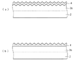
図8は、半導体基板1の受光面側の構造および反射防止層4の形成態様を示す断面模式図である。図8(a)は、第1の実施の形態に係る太陽電池素子100Aが備える構造を示している。すなわち、半導体基板1の受光面自体が凹凸構造を有してなり、その上に形成された反射防止層4についても、係る凹凸構造を引き継ぐ態様にて形成されてなる。   FIG. 8 is a schematic cross-sectional view showing the structure on the light receiving surface side of the semiconductor substrate 1 and the formation mode of the antireflection layer 4. FIG. 8A shows a structure provided in the solar cell element 100A according to the first embodiment. That is, the light-receiving surface itself of the semiconductor substrate 1 has a concavo-convex structure, and the antireflection layer 4 formed thereon is also formed in a manner that inherits the concavo-convex structure.

これに代わり、図8(b)に示すように、半導体基板1の受光面には凹凸構造を形成せず、その上に設けた反射防止層4の表面に凹凸構造を形成するようにしてもよい。係る構造をとる太陽電池素子においても、光の反射損失を低減させる効果が得られる。   Instead of this, as shown in FIG. 8 (b), the uneven structure is not formed on the light receiving surface of the semiconductor substrate 1, and the uneven structure is formed on the surface of the antireflection layer 4 provided thereon. Good. Even in the solar cell element having such a structure, an effect of reducing reflection loss of light can be obtained.

なお、このように表面に凹凸構造を有する反射防止層4の形成は、例えば、表面が平坦な半導体基板1の受光面側にいったん同じく平坦な表面を有するように反射防止層4を形成した上で、エッチング等の処理を施すことによって行うようにしてもよいし、あるいは、膜成長過程において自生的に凹凸構造が形成されるように、反射防止層4の形成条件を適宜に調整することによって行うようにしてもよい。   The antireflection layer 4 having a concavo-convex structure on the surface is formed by, for example, forming the antireflection layer 4 so as to once have a flat surface on the light receiving surface side of the semiconductor substrate 1 having a flat surface. Then, it may be performed by performing a treatment such as etching, or by appropriately adjusting the formation conditions of the antireflection layer 4 so that the concavo-convex structure is spontaneously formed during the film growth process. You may make it perform.

(実施例)
実施例として、第1の実施の形態に係る太陽電池素子100Aについて、厚みt1および厚みt2を(t1>t2の場合を含めて)種々の値とした12種類の太陽電池素子を作成した。12種類の太陽電池素子は互いに、厚みt1および厚みt2の少なくとも一方の大きさが異なるものである。
(Example)
As examples, twelve types of solar cell elements having various values for thickness t1 and thickness t2 (including the case of t1> t2) were created for solar cell element 100A according to the first embodiment. The twelve types of solar cell elements are different from each other in at least one of the thickness t1 and the thickness t2.

半導体基板1としては、大きさが10cm×10cmで、厚みが200μmで、n型のドーパントとしてPが1×10¹⁶(cm-3)の濃度でドープされた多結晶シリコン基板を用意した。係る半導体基板の抵抗率は、0.5Ω・cmであった。 As the semiconductor substrate 1, a polycrystalline silicon substrate having a size of 10 cm × 10 cm, a thickness of 200 μm, and doped with P as a n-type dopant at a concentration of 1 × 10 16 (cm −3 ) was prepared. The resistivity of the semiconductor substrate was 0.5 Ω · cm.

係る半導体基板1の表面を、反応性イオンエッチング法により粗面化した。粗面化は、RIE装置内にて、CHF3を12sccm、Cl2を72sccm、O2を9sccm、およびSF6を65sccmの流量で流し、反応圧力を50mTorrとし、RFパワーを500Wとし、3分間行った。その後、超音波洗浄を行ってエッチング残渣を除去した。 The surface of the semiconductor substrate 1 was roughened by a reactive ion etching method. In the RIE apparatus, CHF 3 is supplied at 12 sccm, Cl 2 is supplied at 72 sccm, O 2 is supplied at 9 sccm, and SF 6 is supplied at a flow rate of 65 sccm. went. Thereafter, ultrasonic cleaning was performed to remove etching residues.

ドープ層3の形成は、熱拡散法を用いた。その際の半導体基板1の加熱温度は800℃とした。なお、マスク20としてはSiO2塗布法により形成した。得られたドープ層3のドーパント濃度は2×10¹⁷(cm-3)であった。 The dope layer 3 was formed using a thermal diffusion method. The heating temperature of the semiconductor substrate 1 at that time was set to 800 ° C. The mask 20 was formed by a SiO 2 coating method. The dopant concentration of the obtained doped layer 3 was 2 × 10 17 (cm −3 ).

i型半導体層5とp型半導体層6とは、PECVD装置を用いて形成した。PECVD装置のチャンバ内のガス圧は、いずれも0.5〜1.5Torr、基板温度はいずれも、130〜170とした。また、原料ガスとしては、i型半導体層5を形成する際には水素とシランとを用い、p型半導体層6を形成する際には、水素とシランとジボランとを用いた。i型半導体層5は、i型半導体5の第1の部分5aの厚みt1を2nm〜10nmの範囲から選択し、かつ、第2の部分5bの厚みt2を2nm〜15nmの範囲から選択して形成した。また、p型半導体層6は、10〜15nmの厚みに形成した。   The i-type semiconductor layer 5 and the p-type semiconductor layer 6 were formed using a PECVD apparatus. The gas pressure in the chamber of the PECVD apparatus was 0.5 to 1.5 Torr for all, and the substrate temperature was 130 to 170 for all. As the source gas, hydrogen and silane were used when the i-type semiconductor layer 5 was formed, and hydrogen, silane and diborane were used when the p-type semiconductor layer 6 was formed. In the i-type semiconductor layer 5, the thickness t1 of the first portion 5a of the i-type semiconductor 5 is selected from the range of 2 nm to 10 nm, and the thickness t2 of the second portion 5b is selected from the range of 2 nm to 15 nm. Formed. The p-type semiconductor layer 6 was formed to a thickness of 10 to 15 nm.

反射防止層4としては、SiN層を100nmの厚みに形成した。SiN層は、PECVD法により、アンモニアと水素とシランとを原料ガスとして形成した。   As the antireflection layer 4, a SiN layer was formed to a thickness of 100 nm. The SiN layer was formed using ammonia, hydrogen, and silane as source gases by PECVD.

第1シード層8および第2シード層11としては、Ni層を0.3μmの厚みに形成した。Ni層は無電解メッキにより形成した。メッキ用の薬液としては、次亜リン酸Niを用い、薬液温度は、90℃以下とした。   As the first seed layer 8 and the second seed layer 11, a Ni layer was formed to a thickness of 0.3 μm. The Ni layer was formed by electroless plating. As a chemical for plating, Ni hypophosphite was used, and the temperature of the chemical was 90 ° C. or less.

第1裏面電極9および第2裏面電極12としては、Cu電極を80μmの厚みに形成した。Cu電極の形成は、電解メッキにより行った。なお、電解メッキ形成後、接着強度向上のため150℃の温度で乾燥処理を行った。   As the 1st back electrode 9 and the 2nd back electrode 12, Cu electrode was formed in thickness of 80 micrometers. The formation of the Cu electrode was performed by electrolytic plating. In addition, after electrolytic plating formation, the drying process was performed at the temperature of 150 degreeC in order to improve adhesive strength.

このようにして作製した12種類の太陽電池素子について、光照射時の電流−電圧特性を測定し、短絡電流Isc、開放電圧Voc、曲線因子FF、および変換効率ηを求めた。 With respect to the 12 types of solar cell elements thus produced, the current-voltage characteristics during light irradiation were measured, and the short circuit current I sc , the open circuit voltage V oc , the fill factor FF, and the conversion efficiency η were determined.

上述のようにして得られた、12種類の実施例に係る太陽電池素子についての評価結果を表1に示す。表1においては、12種類の太陽電池素子の各々を番号1〜12で示している。なお、表1に示す値のうち短絡電流Isc、開放電圧Voc、曲線因子FF、および変換効率ηは、番号5の太陽電池素子について得られた値を1として、規格化したものである。 Table 1 shows the evaluation results of the solar cell elements according to the 12 types of examples obtained as described above. In Table 1, each of 12 types of solar cell elements is indicated by numbers 1-12. Of the values shown in Table 1, the short-circuit current I sc , the open-circuit voltage V oc , the fill factor FF, and the conversion efficiency η are normalized with the value obtained for the solar cell element number 5 as 1. .

Figure 0005174635
Figure 0005174635

表1によれば、番号1〜4の太陽電池素子のいずれにおいても、番号5〜12の太陽電池素子よりも高い変換効率ηが得られたことを示している。すなわち、i型半導体5の第2の部分5bの厚みt2が6nm〜10nmであり、i型半導体5の第1の部分5aの厚みt1が3nm〜5nmであるとき、高い発電効率が得られるといえる。   According to Table 1, it has shown that conversion efficiency (eta) higher than the solar cell element of Nos. 5-12 was obtained in any of the solar cell elements of Nos. 1-4. That is, when the thickness t2 of the second portion 5b of the i-type semiconductor 5 is 6 nm to 10 nm and the thickness t1 of the first portion 5a of the i-type semiconductor 5 is 3 nm to 5 nm, high power generation efficiency is obtained. I can say that.

太陽電池素子100Aの断面構造を示す図である。It is a figure which shows the cross-section of 100 A of solar cell elements. 太陽電池素子100Aの裏面図である。It is a back view of solar cell element 100A. 太陽電池素子100Aの製造工程を示す図である。It is a figure which shows the manufacturing process of 100 A of solar cell elements. 太陽電池素子100Aの製造方法を説明するための工程図である。It is process drawing for demonstrating the manufacturing method of 100 A of solar cell elements. 太陽電池素子100Aの製造方法を説明するための工程図である。It is process drawing for demonstrating the manufacturing method of 100 A of solar cell elements. 太陽電池素子100Aの製造方法を説明するための工程図である。It is process drawing for demonstrating the manufacturing method of 100 A of solar cell elements. 太陽電池素子100Bの断面構造を示す図である。It is a figure which shows the cross-section of the solar cell element 100B. 半導体基板1の受光面側の構造および反射防止層4の形成態様を示す断面模式図である。2 is a schematic cross-sectional view showing a structure of a light receiving surface side of a semiconductor substrate 1 and a formation mode of an antireflection layer 4.

符号の説明Explanation of symbols

1 半導体基板
2 n型半導体領域
3 ドープ層
5 i型半導体層
5a i型半導体5の第1の部分
5b i型半導体5の第2の部分
6 p型半導体層
7 n型電極
8 第1シード層
100A〜B 太陽電池素子
1 semiconductor substrate 2 n-type semiconductor region 3 doped layer 5 i-type semiconductor layer 5a first part of i-type semiconductor 5 5b second part of i-type semiconductor 5 6 p-type semiconductor layer 7 n-type electrode 8 first seed layer 100A-B solar cell element

Claims (7)

第1の面と第2の面とを含み、第1の導電型を有する半導体基板と、
前記第1の導電型に寄与するドーパントを前記半導体基板よりも高い濃度で含有し、前記半導体基板の前記第1の面の第1領域に設けられた第1ドープ層と、
前記半導体基板の前記第1ドープ層上に設けられた第1の部分と、前記半導体基板の前記第1の面の第2領域に設けられた第2の部分と、を含む真性半導体層と、
第2の導電型を有し、前記真性半導体層の前記第2の部分上に設けられた第2の導電型の層と、
を有する太陽電池素子であって
前記真性半導体層の前記第1の部分の厚みが3nm以上5nm以下であり、前記第2の部分の厚みが6nm以上10nm以下であることを特徴とする太陽電池素子。
A semiconductor substrate including a first surface and a second surface and having a first conductivity type;
A dopant that contributes to the first conductivity type at a higher concentration than the semiconductor substrate, and a first doped layer provided in a first region of the first surface of the semiconductor substrate;
An intrinsic semiconductor layer comprising: a first portion provided on the first doped layer of the semiconductor substrate; and a second portion provided in a second region of the first surface of the semiconductor substrate;
A second conductivity type layer having a second conductivity type and provided on the second portion of the intrinsic semiconductor layer;
A solar cell element to have a,
The solar cell element, wherein a thickness of the first portion of the intrinsic semiconductor layer is 3 nm or more and 5 nm or less, and a thickness of the second portion is 6 nm or more and 10 nm or less .
請求項1に記載の太陽電池素子において、
前記第1ドープ層は、前記半導体基板内に設けられていることを特徴とする太陽電池素子。
The solar cell element according to claim 1,
The solar cell element, wherein the first doped layer is provided in the semiconductor substrate.
請求項1または請求項2に記載の太陽電池素子において、
前記第2領域の面積が前記第1領域の面積よりも大きいことを特徴とする太陽電池素子。
In the solar cell element according to claim 1 or 2,
The solar cell element, wherein an area of the second region is larger than an area of the first region .
請求項1ないし請求項3のいずれかに記載の太陽電池素子において、
前記真性半導体層の前記第1の部分に設けられた第1電極と、
前記第2の導電型層上に設けられた第2電極と、
をさらに備え、
前記第1電極と前記第2電極との電気抵抗値が等しいことを特徴とする太陽電池素子。
In the solar cell element according to any one of claims 1 to 3,
A first electrode provided in the first portion of the intrinsic semiconductor layer;
A second electrode provided on the second conductivity type layer;
Further comprising
The solar cell element, wherein the first electrode and the second electrode have the same electrical resistance value .
請求項1ないし請求項4のいずれかに記載の太陽電池素子において、
前記半導体基板の前記第2の面側に、前記第1の導電型に寄与するドーパントを前記半導体基板よりも高い濃度で含有する第2ドープ層をさらに有する、ことを特徴とする太陽電池素子。
In the solar cell element according to any one of claims 1 to 4,
The solar cell element , further comprising a second doped layer containing a dopant contributing to the first conductivity type at a higher concentration than the semiconductor substrate on the second surface side of the semiconductor substrate .
請求項に記載の太陽電池素子において、
前記第1および第2ドープ層が、前記半導体基板の外縁部に熱拡散層として設けられてなる、ことを特徴とする太陽電池素子。
In the solar cell element according to claim 5 ,
The solar cell element, wherein the first and second doped layers are provided as thermal diffusion layers on an outer edge portion of the semiconductor substrate .
請求項1ないし請求項6のいずれかに記載の太陽電池素子において、
前記半導体基板の前記第2の面上に反射防止層をさらに備える、ことを特徴とする太陽電池素子。
Claims 1 in a solar cell element according to claim 6,
A solar cell element , further comprising an antireflection layer on the second surface of the semiconductor substrate .
JP2008304640A 2008-11-28 2008-11-28 Solar cell element Active JP5174635B2 (en)

Priority Applications (1)

Application Number Priority Date Filing Date Title
JP2008304640A JP5174635B2 (en) 2008-11-28 2008-11-28 Solar cell element

Applications Claiming Priority (1)

Application Number Priority Date Filing Date Title
JP2008304640A JP5174635B2 (en) 2008-11-28 2008-11-28 Solar cell element

Publications (2)

Publication Number Publication Date
JP2010129872A JP2010129872A (en) 2010-06-10
JP5174635B2 true JP5174635B2 (en) 2013-04-03

Family

ID=42330047

Family Applications (1)

Application Number Title Priority Date Filing Date
JP2008304640A Active JP5174635B2 (en) 2008-11-28 2008-11-28 Solar cell element

Country Status (1)

Country Link
JP (1) JP5174635B2 (en)

Families Citing this family (11)

* Cited by examiner, † Cited by third party
Publication number Priority date Publication date Assignee Title
KR20120040016A (en) * 2010-10-18 2012-04-26 엘지전자 주식회사 Substrate for solar cell and solar cell
KR101130195B1 (en) 2011-01-10 2012-03-30 엘지전자 주식회사 Solar cell and method for manufacturing the same
US9368655B2 (en) 2010-12-27 2016-06-14 Lg Electronics Inc. Solar cell and method for manufacturing the same
JP2013191656A (en) * 2012-03-13 2013-09-26 Sharp Corp Photoelectric conversion element and manufacturing method thereof
JP5734512B2 (en) 2012-05-14 2015-06-17 三菱電機株式会社 Photoelectric conversion device, manufacturing method thereof, and photoelectric conversion module
JP6599769B2 (en) * 2013-10-25 2019-10-30 シャープ株式会社 Photoelectric conversion device
WO2016076300A1 (en) * 2014-11-14 2016-05-19 シャープ株式会社 Photoelectric conversion element
JP6452011B2 (en) * 2015-05-29 2019-01-16 パナソニックIpマネジメント株式会社 Solar cell
WO2019181834A1 (en) * 2018-03-23 2019-09-26 株式会社カネカ Method for producing solar cell, and solar cell
JP7169440B2 (en) * 2019-04-23 2022-11-10 株式会社カネカ SOLAR CELL MANUFACTURING METHOD AND SOLAR CELL
CN115084312A (en) * 2022-03-11 2022-09-20 浙江爱旭太阳能科技有限公司 Preparation method of solar cell, solar cell module and power generation system

Family Cites Families (5)

* Cited by examiner, † Cited by third party
Publication number Priority date Publication date Assignee Title
JPH0795603B2 (en) * 1990-09-20 1995-10-11 三洋電機株式会社 Photovoltaic device
JP2614561B2 (en) * 1991-10-08 1997-05-28 三洋電機株式会社 Photovoltaic element
JP4155899B2 (en) * 2003-09-24 2008-09-24 三洋電機株式会社 Photovoltaic element manufacturing method
JP3998619B2 (en) * 2003-09-24 2007-10-31 三洋電機株式会社 Photovoltaic element and manufacturing method thereof
JP2006332273A (en) * 2005-05-25 2006-12-07 Sharp Corp Backside contact solar cell

Also Published As

Publication number Publication date
JP2010129872A (en) 2010-06-10

Similar Documents

Publication Publication Date Title
JP5174635B2 (en) Solar cell element
JP5694620B1 (en) Crystalline silicon solar cell manufacturing method and crystalline silicon solar cell module manufacturing method
US9722101B2 (en) Solar cell, solar cell manufacturing method, and solar cell module
JP5774204B2 (en) Photovoltaic element, manufacturing method thereof, and solar cell module
JP2010123859A (en) Solar battery element and production process of solar battery element
JP2010147324A (en) Solar cell element and method of manufacturing solar cell element
JP5891382B2 (en) Method for manufacturing photoelectric conversion element
JP2004266023A (en) Solar battery and method of manufacturing the same
US9640673B2 (en) Solar cell and manufacturing method thereof
JP2013239476A (en) Photovoltaic device and method of manufacturing the same, and photovoltaic module
KR101597532B1 (en) The Manufacturing Method of Back Contact Solar Cells
WO2022142343A1 (en) Solar cell and preparation method therefor
KR20130082066A (en) Photovoltaic device
US9859454B2 (en) Photoelectric conversion device and fabrication method thereof
CN115188837A (en) Back contact solar cell, preparation method and cell module
WO2019163647A1 (en) Method for producing solar cell
Granata et al. Heterojunction interdigitated back-contact solar cells fabricated on wafer bonded to glass
TWI783063B (en) Manufacturing method of solar cell
TW201330304A (en) Method for manufacturing back contact solar cell using punch-through
TW201937748A (en) Method for producing solar cell
JP5645734B2 (en) Solar cell element
JP2011077454A (en) Crystal silicon system solar cell and method of manufacturing the same
JP7237920B2 (en) Solar cell manufacturing method
JP7183245B2 (en) Solar cell manufacturing method
JP5843734B2 (en) Photoelectric conversion element and manufacturing method thereof

Legal Events

Date Code Title Description
A621 Written request for application examination

Free format text: JAPANESE INTERMEDIATE CODE: A621

Effective date: 20110818

A977 Report on retrieval

Free format text: JAPANESE INTERMEDIATE CODE: A971007

Effective date: 20120905

A131 Notification of reasons for refusal

Free format text: JAPANESE INTERMEDIATE CODE: A131

Effective date: 20120911

A521 Request for written amendment filed

Free format text: JAPANESE INTERMEDIATE CODE: A523

Effective date: 20121031

TRDD Decision of grant or rejection written
A01 Written decision to grant a patent or to grant a registration (utility model)

Free format text: JAPANESE INTERMEDIATE CODE: A01

Effective date: 20121204

A61 First payment of annual fees (during grant procedure)

Free format text: JAPANESE INTERMEDIATE CODE: A61

Effective date: 20121228

R150 Certificate of patent or registration of utility model

Ref document number: 5174635

Country of ref document: JP

Free format text: JAPANESE INTERMEDIATE CODE: R150