JP5168866B2 - Power semiconductor module - Google Patents
Power semiconductor module Download PDFInfo
- Publication number
- JP5168866B2 JP5168866B2 JP2006265178A JP2006265178A JP5168866B2 JP 5168866 B2 JP5168866 B2 JP 5168866B2 JP 2006265178 A JP2006265178 A JP 2006265178A JP 2006265178 A JP2006265178 A JP 2006265178A JP 5168866 B2 JP5168866 B2 JP 5168866B2
- Authority
- JP
- Japan
- Prior art keywords
- circuit board
- power semiconductor
- drive circuit
- conductive pattern
- dielectric constant
- Prior art date
- Legal status (The legal status is an assumption and is not a legal conclusion. Google has not performed a legal analysis and makes no representation as to the accuracy of the status listed.)
- Expired - Fee Related
Links
Images


Classifications
-
- H—ELECTRICITY
- H01—ELECTRIC ELEMENTS
- H01L—SEMICONDUCTOR DEVICES NOT COVERED BY CLASS H10
- H01L23/00—Details of semiconductor or other solid state devices
- H01L23/52—Arrangements for conducting electric current within the device in operation from one component to another, i.e. interconnections, e.g. wires, lead frames
- H01L23/538—Arrangements for conducting electric current within the device in operation from one component to another, i.e. interconnections, e.g. wires, lead frames the interconnection structure between a plurality of semiconductor chips being formed on, or in, insulating substrates
- H01L23/5385—Assembly of a plurality of insulating substrates
-
- H—ELECTRICITY
- H01—ELECTRIC ELEMENTS
- H01L—SEMICONDUCTOR DEVICES NOT COVERED BY CLASS H10
- H01L24/00—Arrangements for connecting or disconnecting semiconductor or solid-state bodies; Methods or apparatus related thereto
- H01L24/01—Means for bonding being attached to, or being formed on, the surface to be connected, e.g. chip-to-package, die-attach, "first-level" interconnects; Manufacturing methods related thereto
- H01L24/42—Wire connectors; Manufacturing methods related thereto
- H01L24/47—Structure, shape, material or disposition of the wire connectors after the connecting process
- H01L24/49—Structure, shape, material or disposition of the wire connectors after the connecting process of a plurality of wire connectors
-
- H—ELECTRICITY
- H01—ELECTRIC ELEMENTS
- H01L—SEMICONDUCTOR DEVICES NOT COVERED BY CLASS H10
- H01L25/00—Assemblies consisting of a plurality of individual semiconductor or other solid state devices ; Multistep manufacturing processes thereof
- H01L25/16—Assemblies consisting of a plurality of individual semiconductor or other solid state devices ; Multistep manufacturing processes thereof the devices being of types provided for in two or more different main groups of groups H01L27/00 - H01L33/00, or in a single subclass of H10K, H10N, e.g. forming hybrid circuits
- H01L25/162—Assemblies consisting of a plurality of individual semiconductor or other solid state devices ; Multistep manufacturing processes thereof the devices being of types provided for in two or more different main groups of groups H01L27/00 - H01L33/00, or in a single subclass of H10K, H10N, e.g. forming hybrid circuits the devices being mounted on two or more different substrates
-
- H—ELECTRICITY
- H01—ELECTRIC ELEMENTS
- H01L—SEMICONDUCTOR DEVICES NOT COVERED BY CLASS H10
- H01L2224/00—Indexing scheme for arrangements for connecting or disconnecting semiconductor or solid-state bodies and methods related thereto as covered by H01L24/00
- H01L2224/01—Means for bonding being attached to, or being formed on, the surface to be connected, e.g. chip-to-package, die-attach, "first-level" interconnects; Manufacturing methods related thereto
- H01L2224/42—Wire connectors; Manufacturing methods related thereto
- H01L2224/44—Structure, shape, material or disposition of the wire connectors prior to the connecting process
- H01L2224/45—Structure, shape, material or disposition of the wire connectors prior to the connecting process of an individual wire connector
- H01L2224/45001—Core members of the connector
- H01L2224/45099—Material
- H01L2224/451—Material with a principal constituent of the material being a metal or a metalloid, e.g. boron (B), silicon (Si), germanium (Ge), arsenic (As), antimony (Sb), tellurium (Te) and polonium (Po), and alloys thereof
- H01L2224/45117—Material with a principal constituent of the material being a metal or a metalloid, e.g. boron (B), silicon (Si), germanium (Ge), arsenic (As), antimony (Sb), tellurium (Te) and polonium (Po), and alloys thereof the principal constituent melting at a temperature of greater than or equal to 400°C and less than 950°C
- H01L2224/45124—Aluminium (Al) as principal constituent
-
- H—ELECTRICITY
- H01—ELECTRIC ELEMENTS
- H01L—SEMICONDUCTOR DEVICES NOT COVERED BY CLASS H10
- H01L2224/00—Indexing scheme for arrangements for connecting or disconnecting semiconductor or solid-state bodies and methods related thereto as covered by H01L24/00
- H01L2224/01—Means for bonding being attached to, or being formed on, the surface to be connected, e.g. chip-to-package, die-attach, "first-level" interconnects; Manufacturing methods related thereto
- H01L2224/42—Wire connectors; Manufacturing methods related thereto
- H01L2224/47—Structure, shape, material or disposition of the wire connectors after the connecting process
- H01L2224/48—Structure, shape, material or disposition of the wire connectors after the connecting process of an individual wire connector
- H01L2224/4805—Shape
- H01L2224/4809—Loop shape
- H01L2224/48091—Arched
-
- H—ELECTRICITY
- H01—ELECTRIC ELEMENTS
- H01L—SEMICONDUCTOR DEVICES NOT COVERED BY CLASS H10
- H01L2224/00—Indexing scheme for arrangements for connecting or disconnecting semiconductor or solid-state bodies and methods related thereto as covered by H01L24/00
- H01L2224/01—Means for bonding being attached to, or being formed on, the surface to be connected, e.g. chip-to-package, die-attach, "first-level" interconnects; Manufacturing methods related thereto
- H01L2224/42—Wire connectors; Manufacturing methods related thereto
- H01L2224/47—Structure, shape, material or disposition of the wire connectors after the connecting process
- H01L2224/49—Structure, shape, material or disposition of the wire connectors after the connecting process of a plurality of wire connectors
- H01L2224/491—Disposition
- H01L2224/4911—Disposition the connectors being bonded to at least one common bonding area, e.g. daisy chain
- H01L2224/49111—Disposition the connectors being bonded to at least one common bonding area, e.g. daisy chain the connectors connecting two common bonding areas, e.g. Litz or braid wires
-
- H—ELECTRICITY
- H01—ELECTRIC ELEMENTS
- H01L—SEMICONDUCTOR DEVICES NOT COVERED BY CLASS H10
- H01L2224/00—Indexing scheme for arrangements for connecting or disconnecting semiconductor or solid-state bodies and methods related thereto as covered by H01L24/00
- H01L2224/01—Means for bonding being attached to, or being formed on, the surface to be connected, e.g. chip-to-package, die-attach, "first-level" interconnects; Manufacturing methods related thereto
- H01L2224/42—Wire connectors; Manufacturing methods related thereto
- H01L2224/47—Structure, shape, material or disposition of the wire connectors after the connecting process
- H01L2224/49—Structure, shape, material or disposition of the wire connectors after the connecting process of a plurality of wire connectors
- H01L2224/491—Disposition
- H01L2224/4912—Layout
- H01L2224/49175—Parallel arrangements
-
- H—ELECTRICITY
- H01—ELECTRIC ELEMENTS
- H01L—SEMICONDUCTOR DEVICES NOT COVERED BY CLASS H10
- H01L2224/00—Indexing scheme for arrangements for connecting or disconnecting semiconductor or solid-state bodies and methods related thereto as covered by H01L24/00
- H01L2224/80—Methods for connecting semiconductor or other solid state bodies using means for bonding being attached to, or being formed on, the surface to be connected
- H01L2224/85—Methods for connecting semiconductor or other solid state bodies using means for bonding being attached to, or being formed on, the surface to be connected using a wire connector
- H01L2224/85909—Post-treatment of the connector or wire bonding area
- H01L2224/8592—Applying permanent coating, e.g. protective coating
-
- H—ELECTRICITY
- H01—ELECTRIC ELEMENTS
- H01L—SEMICONDUCTOR DEVICES NOT COVERED BY CLASS H10
- H01L24/00—Arrangements for connecting or disconnecting semiconductor or solid-state bodies; Methods or apparatus related thereto
- H01L24/01—Means for bonding being attached to, or being formed on, the surface to be connected, e.g. chip-to-package, die-attach, "first-level" interconnects; Manufacturing methods related thereto
- H01L24/42—Wire connectors; Manufacturing methods related thereto
- H01L24/44—Structure, shape, material or disposition of the wire connectors prior to the connecting process
- H01L24/45—Structure, shape, material or disposition of the wire connectors prior to the connecting process of an individual wire connector
-
- H—ELECTRICITY
- H01—ELECTRIC ELEMENTS
- H01L—SEMICONDUCTOR DEVICES NOT COVERED BY CLASS H10
- H01L24/00—Arrangements for connecting or disconnecting semiconductor or solid-state bodies; Methods or apparatus related thereto
- H01L24/01—Means for bonding being attached to, or being formed on, the surface to be connected, e.g. chip-to-package, die-attach, "first-level" interconnects; Manufacturing methods related thereto
- H01L24/42—Wire connectors; Manufacturing methods related thereto
- H01L24/47—Structure, shape, material or disposition of the wire connectors after the connecting process
- H01L24/48—Structure, shape, material or disposition of the wire connectors after the connecting process of an individual wire connector
-
- H—ELECTRICITY
- H01—ELECTRIC ELEMENTS
- H01L—SEMICONDUCTOR DEVICES NOT COVERED BY CLASS H10
- H01L25/00—Assemblies consisting of a plurality of individual semiconductor or other solid state devices ; Multistep manufacturing processes thereof
- H01L25/03—Assemblies consisting of a plurality of individual semiconductor or other solid state devices ; Multistep manufacturing processes thereof all the devices being of a type provided for in the same subgroup of groups H01L27/00 - H01L33/00, or in a single subclass of H10K, H10N, e.g. assemblies of rectifier diodes
- H01L25/04—Assemblies consisting of a plurality of individual semiconductor or other solid state devices ; Multistep manufacturing processes thereof all the devices being of a type provided for in the same subgroup of groups H01L27/00 - H01L33/00, or in a single subclass of H10K, H10N, e.g. assemblies of rectifier diodes the devices not having separate containers
- H01L25/07—Assemblies consisting of a plurality of individual semiconductor or other solid state devices ; Multistep manufacturing processes thereof all the devices being of a type provided for in the same subgroup of groups H01L27/00 - H01L33/00, or in a single subclass of H10K, H10N, e.g. assemblies of rectifier diodes the devices not having separate containers the devices being of a type provided for in group H01L29/00
- H01L25/072—Assemblies consisting of a plurality of individual semiconductor or other solid state devices ; Multistep manufacturing processes thereof all the devices being of a type provided for in the same subgroup of groups H01L27/00 - H01L33/00, or in a single subclass of H10K, H10N, e.g. assemblies of rectifier diodes the devices not having separate containers the devices being of a type provided for in group H01L29/00 the devices being arranged next to each other
-
- H—ELECTRICITY
- H01—ELECTRIC ELEMENTS
- H01L—SEMICONDUCTOR DEVICES NOT COVERED BY CLASS H10
- H01L25/00—Assemblies consisting of a plurality of individual semiconductor or other solid state devices ; Multistep manufacturing processes thereof
- H01L25/18—Assemblies consisting of a plurality of individual semiconductor or other solid state devices ; Multistep manufacturing processes thereof the devices being of types provided for in two or more different subgroups of the same main group of groups H01L27/00 - H01L33/00, or in a single subclass of H10K, H10N
-
- H—ELECTRICITY
- H01—ELECTRIC ELEMENTS
- H01L—SEMICONDUCTOR DEVICES NOT COVERED BY CLASS H10
- H01L2924/00—Indexing scheme for arrangements or methods for connecting or disconnecting semiconductor or solid-state bodies as covered by H01L24/00
- H01L2924/01—Chemical elements
- H01L2924/01006—Carbon [C]
-
- H—ELECTRICITY
- H01—ELECTRIC ELEMENTS
- H01L—SEMICONDUCTOR DEVICES NOT COVERED BY CLASS H10
- H01L2924/00—Indexing scheme for arrangements or methods for connecting or disconnecting semiconductor or solid-state bodies as covered by H01L24/00
- H01L2924/01—Chemical elements
- H01L2924/01013—Aluminum [Al]
-
- H—ELECTRICITY
- H01—ELECTRIC ELEMENTS
- H01L—SEMICONDUCTOR DEVICES NOT COVERED BY CLASS H10
- H01L2924/00—Indexing scheme for arrangements or methods for connecting or disconnecting semiconductor or solid-state bodies as covered by H01L24/00
- H01L2924/01—Chemical elements
- H01L2924/01014—Silicon [Si]
-
- H—ELECTRICITY
- H01—ELECTRIC ELEMENTS
- H01L—SEMICONDUCTOR DEVICES NOT COVERED BY CLASS H10
- H01L2924/00—Indexing scheme for arrangements or methods for connecting or disconnecting semiconductor or solid-state bodies as covered by H01L24/00
- H01L2924/01—Chemical elements
- H01L2924/01029—Copper [Cu]
-
- H—ELECTRICITY
- H01—ELECTRIC ELEMENTS
- H01L—SEMICONDUCTOR DEVICES NOT COVERED BY CLASS H10
- H01L2924/00—Indexing scheme for arrangements or methods for connecting or disconnecting semiconductor or solid-state bodies as covered by H01L24/00
- H01L2924/01—Chemical elements
- H01L2924/01033—Arsenic [As]
-
- H—ELECTRICITY
- H01—ELECTRIC ELEMENTS
- H01L—SEMICONDUCTOR DEVICES NOT COVERED BY CLASS H10
- H01L2924/00—Indexing scheme for arrangements or methods for connecting or disconnecting semiconductor or solid-state bodies as covered by H01L24/00
- H01L2924/01—Chemical elements
- H01L2924/01058—Cerium [Ce]
-
- H—ELECTRICITY
- H01—ELECTRIC ELEMENTS
- H01L—SEMICONDUCTOR DEVICES NOT COVERED BY CLASS H10
- H01L2924/00—Indexing scheme for arrangements or methods for connecting or disconnecting semiconductor or solid-state bodies as covered by H01L24/00
- H01L2924/01—Chemical elements
- H01L2924/01068—Erbium [Er]
-
- H—ELECTRICITY
- H01—ELECTRIC ELEMENTS
- H01L—SEMICONDUCTOR DEVICES NOT COVERED BY CLASS H10
- H01L2924/00—Indexing scheme for arrangements or methods for connecting or disconnecting semiconductor or solid-state bodies as covered by H01L24/00
- H01L2924/01—Chemical elements
- H01L2924/01082—Lead [Pb]
-
- H—ELECTRICITY
- H01—ELECTRIC ELEMENTS
- H01L—SEMICONDUCTOR DEVICES NOT COVERED BY CLASS H10
- H01L2924/00—Indexing scheme for arrangements or methods for connecting or disconnecting semiconductor or solid-state bodies as covered by H01L24/00
- H01L2924/013—Alloys
- H01L2924/014—Solder alloys
-
- H—ELECTRICITY
- H01—ELECTRIC ELEMENTS
- H01L—SEMICONDUCTOR DEVICES NOT COVERED BY CLASS H10
- H01L2924/00—Indexing scheme for arrangements or methods for connecting or disconnecting semiconductor or solid-state bodies as covered by H01L24/00
- H01L2924/10—Details of semiconductor or other solid state devices to be connected
- H01L2924/11—Device type
- H01L2924/13—Discrete devices, e.g. 3 terminal devices
- H01L2924/1304—Transistor
- H01L2924/1305—Bipolar Junction Transistor [BJT]
- H01L2924/13055—Insulated gate bipolar transistor [IGBT]
-
- H—ELECTRICITY
- H01—ELECTRIC ELEMENTS
- H01L—SEMICONDUCTOR DEVICES NOT COVERED BY CLASS H10
- H01L2924/00—Indexing scheme for arrangements or methods for connecting or disconnecting semiconductor or solid-state bodies as covered by H01L24/00
- H01L2924/15—Details of package parts other than the semiconductor or other solid state devices to be connected
- H01L2924/181—Encapsulation
Landscapes
- Engineering & Computer Science (AREA)
- Microelectronics & Electronic Packaging (AREA)
- Computer Hardware Design (AREA)
- Power Engineering (AREA)
- Physics & Mathematics (AREA)
- Condensed Matter Physics & Semiconductors (AREA)
- General Physics & Mathematics (AREA)
- Cooling Or The Like Of Semiconductors Or Solid State Devices (AREA)
- Inverter Devices (AREA)
Description
本発明は、部分放電を低減することにより、製品の長寿命化が可能となるパワー半導体モジュールに関するものである。 The present invention relates to a power semiconductor module that can extend the life of a product by reducing partial discharge.
従来のパワー半導体モジュールとして、放熱板と、放熱板上に取り付けられた回路基板と、回路基板上に設けられた導電パターンと、回路基板を囲うように放熱板上に設けられたケースと、ケース内に充填された柔軟絶縁物とを有し、そして絶縁耐圧特性の信頼性向上の観点から導電パターンの外周部に接して回路基板の上面に固体絶縁物を設けるようにしたものが提案されている(例えば、特許文献1参照)。 As a conventional power semiconductor module, a heat sink, a circuit board mounted on the heat sink, a conductive pattern provided on the circuit board, a case provided on the heat sink so as to surround the circuit board, and a case In order to improve the reliability of the withstand voltage characteristics, a solid insulator is provided on the upper surface of the circuit board in contact with the outer periphery of the conductive pattern. (For example, refer to Patent Document 1).
しかし、パワー半導体モジュールは、高印加電圧中で使用されることにより、パワー半導体モジュールの内部の浮遊電位部分から部分放電が発生し、絶縁不良を生じる場合がある。特に、複雑な形状をした両面電極付駆動回路基板では部分放電が発生しやすいことが判明している。 However, when the power semiconductor module is used in a high applied voltage, a partial discharge may occur from a floating potential portion inside the power semiconductor module, resulting in an insulation failure. In particular, it has been found that a partial discharge is likely to occur in a drive circuit board with a double-sided electrode having a complicated shape.
本発明は、上述のような課題を解決するためになされたもので、その目的は、部分放電を低減することにより、製品の長寿命化が可能となるパワー半導体モジュールを得るものである。 The present invention has been made to solve the above-described problems, and an object of the present invention is to obtain a power semiconductor module capable of extending the life of a product by reducing partial discharge.
本発明に係るパワー半導体モジュールは、放熱板と、前記放熱板上に取り付けられ、パワー半導体素子を備えたパワー半導体回路基板と、前記放熱板上に取り付けられ、前記パワー半導体素子の電極とワイヤにより接続され、前記パワー半導体素子にオン・オフ信号を送るように構成された駆動回路基板と、前記パワー半導体回路基板及び前記駆動回路基板を囲うように前記放熱板上に設けられたケースと、前記ケース内に充填された柔軟絶縁物とを有し、前記駆動回路基板は、絶縁基板と、前記絶縁基板上に設けられた導電パターンと、前記導電パターンに接続されたチップ抵抗と、前記導電パターンを覆い、前記柔軟絶縁物よりも低い誘電率を持つ低誘電率膜とを有し、前記パワー半導体素子及び前記パワー半導体回路基板は、前記低誘電率膜により覆われていない。本発明のその他の特徴は以下に明らかにする。
A power semiconductor module according to the present invention includes a heat sink, a power semiconductor circuit board having a power semiconductor element attached on the heat sink, and an electrode and a wire of the power semiconductor element attached on the heat sink. A drive circuit board connected and configured to send an on / off signal to the power semiconductor element; a case provided on the heat sink so as to surround the power semiconductor circuit board and the drive circuit board; A flexible insulating material filled in a case, wherein the drive circuit board is an insulating board, a conductive pattern provided on the insulating board, a chip resistor connected to the conductive pattern, and the conductive pattern the cover, the flexible insulator and a low dielectric constant film having a dielectric constant lower than that, the power semiconductor element and the power semiconductor circuit substrate, the low induction Not covered by the rate film. Other features of the present invention will become apparent below.
本発明により、部分放電を低減することにより、製品の長寿命化が可能となる。 According to the present invention, the product life can be extended by reducing the partial discharge.
実施の形態1.
図1は、本発明の実施の形態1に係るパワー半導体モジュールを示す断面図であり、図2はその上面図である。このパワー半導体モジュールは、複数のIGBTを並列接続し、共通のコレクタ端子、エミッタ端子、ゲート端子を備えることで高耐圧・大電流特性を得るように構成された回路ブロックを複数内蔵している。参考までにその1ブロックについて等価回路で表すと図3のようになる。
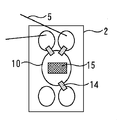
FIG. 1 is a sectional view showing a power semiconductor module according to
金属製のベース板1(放熱板)上に、駆動回路基板2(回路基板)とパワー半導体回路基板3、中継回路基板13が取り付けられている。それぞれの回路基板は、セラミックスなどの絶縁基板の両面に銅又はアルミ等からなる導電(電極)パターン10が設けられるようにして構成されており、パワー半導体回路基板3の導電パターン上には絶縁ゲート型バイポーラトランジスタ(IGBT)4aとフリーホイールダイオード(FWDi)4bなどのパワー半導体素子(チップ)4が、また駆動回路基板2の導電パターン上にはチップ抵抗14がはんだ等の導電性接着部材を使って接合されている。パワー半導体素子4における電極(IGBT4aのエミッタ、ゲート及びFWDi4bにおけるアノード)は、Alなどのワイヤ5を使って、駆動回路基板2や中継回路基板13に電気的に接続されている。ここで整理をしておくと、IGBT4aのエミッタ電極とFWDi4bのアノード電極は中継回路基板の導電パターン10に、IGBT4aのゲート電極は駆動回路基板2の導電パターン10にそれぞれワイヤ5を介して接続され、IGBT4aのコレクタ電極とFWDi4bのカソード電極とは互いにパワー半導体回路基板3の導電パターン10を介して接続されている。そして、駆動回路基板2、パワー半導体回路基板3及び中継回路基板13を囲うようにベース板1上に樹脂性のケース7が設けられ、ケース7の上部にふた8が配置されている。さらに、ケース7内には、気密性と絶縁を保つためシリコンゲル9(柔軟絶縁物)が充填されている。また、それぞれの回路基板は電極端子接合領域15を備え、この電極端子接合領域15には図示していないが装置外部との電気的接続を実現する電極端子が取り付けられている。なお、この説明にあたっては、パワー半導体回路基板3と中継回路基板13とは異なる基板として分離されているが、同じ1つの絶縁基板上に導電パターンの形成領域を分けて構成されるようにしてもよい。
A drive circuit board 2 (circuit board), a power
図4は、図1のA部の拡大断面図である。駆動回路基板2上には、銅、アルミ等の金属から成る導電パターン10が設けられている。そして、導電パターン10を覆うように低誘電率膜11が設けられている。これにより、複雑な形状をした駆動回路基板2における部分放電を低減することができるため、製品の長寿命化が可能となる。なお、パワー半導体回路基板3及び中継回路基板13については、従来技術と同様に導電パターンの外周部に接して絶縁基板の上面に低誘電率膜11を設けるようにすることで絶縁耐圧の向上は望め、駆動回路基板2のように導電パターンを覆う必要はない。
4 is an enlarged cross-sectional view of a portion A in FIG. A
ここで、低誘電率膜11として、シリコンゴム、ポリイミド、エポキシ樹脂などを用いることができる。特に、低誘電率膜11としてシリコンゴムを用いればアセンブリが容易となり、ポリイミドを用いれば耐熱性が向上し、エポキシ樹脂を用いればヒートサイクル性が向上する。
Here, as the low dielectric
なお、低誘電率膜11の形成工程に関して簡単に説明しておくと、駆動回路基板2の場合、まず駆動回路基板2の導電パターン上における所定の位置にチップ抵抗14をはんだ等により接合し、駆動回路基板2の導電パターンにおけるワイヤボンディング位置とパワー半導体回路基板3上のパワー半導体素子4、具体的にはIGBT4aのゲート電極との間をアルミワイヤの超音波接合などによって繋ぐ。次に、電極端子を導電パターン10における電極端子接合領域15にはんだ等により接合した後、導電パターン10を覆うように低誘電率膜11を塗布する。一方、パワー半導体回路基板3や中継回路基板13における低誘電率膜11の形成は、パワー半導体回路基板3の導電パターン上における所定の位置にパワー半導体素子4をはんだ等で接合した後、ワイヤボンディングや電極端子の接合を行う前に、導電パターンの外周部に接して絶縁基板の上面に塗布する。
The process for forming the low dielectric
実施の形態2.
図5は、本発明の実施の形態2に係る駆動回路基板を示す上面図である。本実施の形態では、導電パターン10のコーナー部が丸い。その他の構成は実施の形態1と同様である。これにより、実施の形態1よりも部分放電を低減することができるため、製品の更なる長寿命化が可能となる。
FIG. 5 is a top view showing a drive circuit board according to
実施の形態3.
図6は、本発明の実施の形態3に係る駆動回路基板を示す上面図である。本実施の形態では、導電パターン10が円状である。そして、導電パターン10を低誘電率膜11で覆っていない。その他の構成は実施の形態1と同様である。これにより、複雑な形状をした駆動回路基板2における部分放電を低減することができるため、製品の長寿命化が可能となる。
FIG. 6 is a top view showing a drive circuit board according to
実施の形態4.
図7は、本発明の実施の形態4に係る駆動回路基板を示す上面図である。本実施の形態では、導電パターン10を低誘電率膜11で覆っている。その他の構成は実施の形態3と同様である。これにより、実施の形態3よりも部分放電を低減することができるため、製品の更なる長寿命化が可能となる。
Embodiment 4 FIG.
FIG. 7 is a top view showing a drive circuit board according to Embodiment 4 of the present invention. In the present embodiment, the
1 ベース板(放熱板)
2 両面電極付駆動回路基板(回路基板)
7 ケース
8 ふた
9 シリコンゲル(柔軟絶縁物)
10 導電パターン
11 低誘電率膜
1 Base plate (heat sink)
2 Double-sided drive circuit board (circuit board)
7 Case 8 Lid 9 Silicon gel (flexible insulator)
10
Claims (4)
前記放熱板上に取り付けられ、パワー半導体素子を備えたパワー半導体回路基板と、
前記放熱板上に取り付けられ、前記パワー半導体素子の電極とワイヤにより接続され、前記パワー半導体素子にオン・オフ信号を送るように構成された駆動回路基板と、
前記パワー半導体回路基板及び前記駆動回路基板を囲うように前記放熱板上に設けられたケースと、
前記ケース内に充填された柔軟絶縁物とを有し、
前記駆動回路基板は、
絶縁基板と、
前記絶縁基板上に設けられた導電パターンと、
前記導電パターンに接続されたチップ抵抗と、
前記導電パターンを覆い、前記柔軟絶縁物よりも低い誘電率を持つ低誘電率膜とを有し、
前記パワー半導体素子及び前記パワー半導体回路基板は、前記低誘電率膜により覆われていないことを特徴とするパワー半導体モジュール。 A heat sink,
A power semiconductor circuit board mounted on the heat sink and provided with a power semiconductor element;
A drive circuit board mounted on the heat sink, connected to an electrode of the power semiconductor element by a wire, and configured to send an on / off signal to the power semiconductor element;
A case provided on the heat sink so as to surround the power semiconductor circuit board and the drive circuit board;
A flexible insulator filled in the case;
The drive circuit board is
An insulating substrate;
A conductive pattern provided on the insulating substrate;
A chip resistor connected to the conductive pattern;
A low dielectric constant film covering the conductive pattern and having a dielectric constant lower than that of the flexible insulator;
The power semiconductor module and the power semiconductor circuit board are not covered with the low dielectric constant film.
前記駆動回路基板を外部装置に相互接続する電極端子接合領域を有する第1パターンと、
自身を前記パワー半導体素子に相互接続するワイヤボンディング位置を有する第2パターンとを有し、
前記チップ抵抗は、前記第1パターンと前記第2パターンを電気的に接続することを特徴とする請求項1又は2に記載のパワー半導体モジュール。 The conductive pattern of the drive circuit board is:
A first pattern having electrode terminal bonding regions interconnecting the drive circuit board to an external device;
A second pattern having a wire bonding position interconnecting itself to the power semiconductor element;
The power semiconductor module according to claim 1, wherein the chip resistor electrically connects the first pattern and the second pattern.
Priority Applications (5)
| Application Number | Priority Date | Filing Date | Title |
|---|---|---|---|
| JP2006265178A JP5168866B2 (en) | 2006-09-28 | 2006-09-28 | Power semiconductor module |
| US11/566,274 US7514777B2 (en) | 2006-09-28 | 2006-12-04 | Power semiconductor module |
| FR0701021A FR2906645A1 (en) | 2006-09-28 | 2007-02-13 | POWER SEMICONDUCTOR MODULE |
| DE102007015534.6A DE102007015534B4 (en) | 2006-09-28 | 2007-03-30 | The power semiconductor module |
| CN2007100921942A CN101154653B (en) | 2006-09-28 | 2007-03-30 | Power semiconductor module |
Applications Claiming Priority (1)
| Application Number | Priority Date | Filing Date | Title |
|---|---|---|---|
| JP2006265178A JP5168866B2 (en) | 2006-09-28 | 2006-09-28 | Power semiconductor module |
Publications (3)
| Publication Number | Publication Date |
|---|---|
| JP2008085169A JP2008085169A (en) | 2008-04-10 |
| JP2008085169A5 JP2008085169A5 (en) | 2009-07-30 |
| JP5168866B2 true JP5168866B2 (en) | 2013-03-27 |
Family
ID=39134590
Family Applications (1)
| Application Number | Title | Priority Date | Filing Date |
|---|---|---|---|
| JP2006265178A Expired - Fee Related JP5168866B2 (en) | 2006-09-28 | 2006-09-28 | Power semiconductor module |
Country Status (5)
| Country | Link |
|---|---|
| US (1) | US7514777B2 (en) |
| JP (1) | JP5168866B2 (en) |
| CN (1) | CN101154653B (en) |
| DE (1) | DE102007015534B4 (en) |
| FR (1) | FR2906645A1 (en) |
Families Citing this family (17)
| Publication number | Priority date | Publication date | Assignee | Title |
|---|---|---|---|---|
| JPS5834532B2 (en) * | 1979-12-07 | 1983-07-27 | 新日本製鐵株式会社 | Finish annealing method for grain-oriented electrical steel sheets |
| EP2182551A1 (en) * | 2008-10-29 | 2010-05-05 | ABB Research Ltd. | Connection arrangement for semiconductor power modules |
| WO2010131679A1 (en) * | 2009-05-14 | 2010-11-18 | ローム株式会社 | Semiconductor device |
| DE102009026558B3 (en) * | 2009-05-28 | 2010-12-02 | Infineon Technologies Ag | Power semiconductor module with movably mounted circuit carriers and method for producing such a power semiconductor module |
| US8076696B2 (en) * | 2009-10-30 | 2011-12-13 | General Electric Company | Power module assembly with reduced inductance |
| CN109166833B (en) * | 2010-01-15 | 2022-04-08 | 三菱电机株式会社 | Power semiconductor module |
| JP5212417B2 (en) | 2010-04-12 | 2013-06-19 | 三菱電機株式会社 | Power semiconductor module |
| JP5174085B2 (en) * | 2010-05-20 | 2013-04-03 | 三菱電機株式会社 | Semiconductor device |
| US9129932B2 (en) * | 2011-06-27 | 2015-09-08 | Rohm Co., Ltd. | Semiconductor module |
| CN102364676B (en) * | 2011-11-30 | 2013-10-30 | 江苏宏微科技有限公司 | Packaging shell structure for semiconductor power module |
| US9890470B2 (en) * | 2012-01-30 | 2018-02-13 | Kyocera Corporation | Seed crystal holder for growing a crystal by a solution method |
| DE102012211446B4 (en) * | 2012-07-02 | 2016-05-12 | Infineon Technologies Ag | EXPLOSION-PROTECTED SEMICONDUCTOR MODULE |
| DE112013007691T5 (en) * | 2013-12-17 | 2016-09-22 | Mitsubishi Electric Corporation | The power semiconductor module |
| CN103675640A (en) * | 2013-12-19 | 2014-03-26 | 江苏瑞新科技股份有限公司 | Semiconductor P and N type non-contact test sensor |
| JP6166701B2 (en) * | 2014-08-22 | 2017-07-19 | 株式会社東芝 | Semiconductor device |
| JP6809294B2 (en) * | 2017-03-02 | 2021-01-06 | 三菱電機株式会社 | Power module |
| CN113707643A (en) * | 2021-08-30 | 2021-11-26 | 中国振华集团永光电子有限公司(国营第八七三厂) | High-integration high-reliability IGBT power module and manufacturing method thereof |
Family Cites Families (16)
| Publication number | Priority date | Publication date | Assignee | Title |
|---|---|---|---|---|
| CH560999A5 (en) | 1973-08-16 | 1975-04-15 | Bbc Brown Boveri & Cie | |
| JP2726515B2 (en) * | 1989-09-22 | 1998-03-11 | 電気化学工業株式会社 | Semiconductor tower mounting circuit board and method of manufacturing the same |
| US5744860A (en) | 1996-02-06 | 1998-04-28 | Asea Brown Boveri Ag | Power semiconductor module |
| EP0789397B1 (en) | 1996-02-07 | 2004-05-06 | Hitachi, Ltd. | Circuit board and semiconductor device using the circuit board |
| JP3206717B2 (en) * | 1996-04-02 | 2001-09-10 | 富士電機株式会社 | Power semiconductor module |
| JP3599517B2 (en) | 1997-01-29 | 2004-12-08 | 電気化学工業株式会社 | Circuit board for power module |
| JP2000323647A (en) * | 1999-05-12 | 2000-11-24 | Toshiba Corp | Module semiconductor device and manufacture thereof |
| US7173336B2 (en) * | 2000-01-31 | 2007-02-06 | Sanyo Electric Co., Ltd. | Hybrid integrated circuit device |
| JP2002076197A (en) | 2000-08-24 | 2002-03-15 | Toshiba Corp | Board for semiconductor device and semiconductor device |
| JP3923716B2 (en) * | 2000-09-29 | 2007-06-06 | 株式会社東芝 | Semiconductor device |
| US20020043727A1 (en) * | 2000-10-13 | 2002-04-18 | Hsiao-Che Wu | Bonding pad structure |
| US6844621B2 (en) | 2002-08-13 | 2005-01-18 | Fuji Electric Co., Ltd. | Semiconductor device and method of relaxing thermal stress |
| JP4381047B2 (en) | 2003-07-09 | 2009-12-09 | 東芝三菱電機産業システム株式会社 | Semiconductor device |
| JP4037332B2 (en) * | 2003-07-10 | 2008-01-23 | シャープ株式会社 | IC module and IC card |
| JP4097613B2 (en) * | 2004-03-09 | 2008-06-11 | 三菱電機株式会社 | Semiconductor device |
| JP4376106B2 (en) | 2004-03-30 | 2009-12-02 | 電気化学工業株式会社 | Ceramic double-layer circuit board |
-
2006
- 2006-09-28 JP JP2006265178A patent/JP5168866B2/en not_active Expired - Fee Related
- 2006-12-04 US US11/566,274 patent/US7514777B2/en active Active
-
2007
- 2007-02-13 FR FR0701021A patent/FR2906645A1/en active Pending
- 2007-03-30 CN CN2007100921942A patent/CN101154653B/en not_active Expired - Fee Related
- 2007-03-30 DE DE102007015534.6A patent/DE102007015534B4/en not_active Expired - Fee Related
Also Published As
| Publication number | Publication date |
|---|---|
| US20080105896A1 (en) | 2008-05-08 |
| DE102007015534A1 (en) | 2008-04-03 |
| FR2906645A1 (en) | 2008-04-04 |
| CN101154653A (en) | 2008-04-02 |
| US7514777B2 (en) | 2009-04-07 |
| CN101154653B (en) | 2010-05-26 |
| DE102007015534B4 (en) | 2015-01-22 |
| JP2008085169A (en) | 2008-04-10 |
Similar Documents
| Publication | Publication Date | Title |
|---|---|---|
| JP5168866B2 (en) | Power semiconductor module | |
| JP5212417B2 (en) | Power semiconductor module | |
| US8324726B2 (en) | Semiconductor device, electrode member and electrode member fabrication method | |
| US9129931B2 (en) | Power semiconductor module and power unit device | |
| JP5789264B2 (en) | Circuit equipment | |
| WO2015174158A1 (en) | Power semiconductor module and composite module | |
| JP6439389B2 (en) | Semiconductor device | |
| US9466542B2 (en) | Semiconductor device | |
| KR101734712B1 (en) | Power module | |
| US5063434A (en) | Plastic molded type power semiconductor device | |
| JP6226068B2 (en) | Semiconductor device | |
| JP4061551B2 (en) | Semiconductor device | |
| WO2013065462A1 (en) | Semiconductor device and manufacturing method therefor | |
| JP6248803B2 (en) | Power semiconductor module | |
| JP2005129826A (en) | Power semiconductor device | |
| KR101766082B1 (en) | Power module | |
| JP2004088022A (en) | High power semiconductor device | |
| JP2017135144A (en) | Semiconductor module | |
| JP4150508B2 (en) | Power semiconductor device | |
| WO2023214500A1 (en) | Semiconductor device | |
| JP2013051300A (en) | Semiconductor module | |
| JP2017059781A (en) | Semiconductor module, driving device including the same, power steering apparatus, and vehicle | |
| JP2003273318A (en) | Electric power semiconductor module | |
| JP2003060152A (en) | Semiconductor device |
Legal Events
| Date | Code | Title | Description |
|---|---|---|---|
| A521 | Request for written amendment filed |
Free format text: JAPANESE INTERMEDIATE CODE: A523 Effective date: 20090611 |
|
| A621 | Written request for application examination |
Free format text: JAPANESE INTERMEDIATE CODE: A621 Effective date: 20090611 |
|
| A977 | Report on retrieval |
Free format text: JAPANESE INTERMEDIATE CODE: A971007 Effective date: 20091208 |
|
| A131 | Notification of reasons for refusal |
Free format text: JAPANESE INTERMEDIATE CODE: A131 Effective date: 20120214 |
|
| A521 | Request for written amendment filed |
Free format text: JAPANESE INTERMEDIATE CODE: A523 Effective date: 20120406 |
|
| A131 | Notification of reasons for refusal |
Free format text: JAPANESE INTERMEDIATE CODE: A131 Effective date: 20120904 |
|
| A521 | Request for written amendment filed |
Free format text: JAPANESE INTERMEDIATE CODE: A523 Effective date: 20121004 |
|
| TRDD | Decision of grant or rejection written | ||
| A01 | Written decision to grant a patent or to grant a registration (utility model) |
Free format text: JAPANESE INTERMEDIATE CODE: A01 Effective date: 20121204 |
|
| A61 | First payment of annual fees (during grant procedure) |
Free format text: JAPANESE INTERMEDIATE CODE: A61 Effective date: 20121217 |
|
| R150 | Certificate of patent or registration of utility model |
Ref document number: 5168866 Country of ref document: JP Free format text: JAPANESE INTERMEDIATE CODE: R150 |
|
| R250 | Receipt of annual fees |
Free format text: JAPANESE INTERMEDIATE CODE: R250 |
|
| R250 | Receipt of annual fees |
Free format text: JAPANESE INTERMEDIATE CODE: R250 |
|
| R250 | Receipt of annual fees |
Free format text: JAPANESE INTERMEDIATE CODE: R250 |
|
| R250 | Receipt of annual fees |
Free format text: JAPANESE INTERMEDIATE CODE: R250 |
|
| R250 | Receipt of annual fees |
Free format text: JAPANESE INTERMEDIATE CODE: R250 |
|
| R250 | Receipt of annual fees |
Free format text: JAPANESE INTERMEDIATE CODE: R250 |
|
| LAPS | Cancellation because of no payment of annual fees |