JP5138407B2 - Wafer and wafer polishing method - Google Patents
Wafer and wafer polishing method Download PDFInfo
- Publication number
- JP5138407B2 JP5138407B2 JP2008033070A JP2008033070A JP5138407B2 JP 5138407 B2 JP5138407 B2 JP 5138407B2 JP 2008033070 A JP2008033070 A JP 2008033070A JP 2008033070 A JP2008033070 A JP 2008033070A JP 5138407 B2 JP5138407 B2 JP 5138407B2
- Authority
- JP
- Japan
- Prior art keywords
- wafer
- curved surface
- polishing
- carrier
- corners
- Prior art date
- Legal status (The legal status is an assumption and is not a legal conclusion. Google has not performed a legal analysis and makes no representation as to the accuracy of the status listed.)
- Active
Links
- 238000005498 polishing Methods 0.000 title claims description 183
- 238000000034 method Methods 0.000 title claims description 81
- 239000007788 liquid Substances 0.000 claims description 80
- 239000013078 crystal Substances 0.000 claims description 18
- 230000002093 peripheral effect Effects 0.000 claims description 18
- 239000002994 raw material Substances 0.000 claims description 13
- 230000007246 mechanism Effects 0.000 claims description 12
- 235000012431 wafers Nutrition 0.000 description 234
- 238000004519 manufacturing process Methods 0.000 description 50
- 230000008569 process Effects 0.000 description 34
- 238000005530 etching Methods 0.000 description 31
- 230000005284 excitation Effects 0.000 description 30
- 229910052751 metal Inorganic materials 0.000 description 21
- 239000002184 metal Substances 0.000 description 21
- 239000000843 powder Substances 0.000 description 20
- 235000014676 Phragmites communis Nutrition 0.000 description 17
- 239000000463 material Substances 0.000 description 16
- 238000007517 polishing process Methods 0.000 description 16
- 239000002585 base Substances 0.000 description 15
- 230000006870 function Effects 0.000 description 14
- 238000000059 patterning Methods 0.000 description 14
- 238000007789 sealing Methods 0.000 description 13
- 238000000605 extraction Methods 0.000 description 12
- 230000001681 protective effect Effects 0.000 description 12
- 238000004891 communication Methods 0.000 description 11
- 238000005520 cutting process Methods 0.000 description 11
- 229920002120 photoresistant polymer Polymers 0.000 description 10
- 239000004575 stone Substances 0.000 description 10
- 238000004140 cleaning Methods 0.000 description 9
- 239000000945 filler Substances 0.000 description 9
- 238000007747 plating Methods 0.000 description 9
- 239000006061 abrasive grain Substances 0.000 description 8
- 238000011084 recovery Methods 0.000 description 8
- XLYOFNOQVPJJNP-UHFFFAOYSA-N water Substances O XLYOFNOQVPJJNP-UHFFFAOYSA-N 0.000 description 8
- 244000273256 Phragmites communis Species 0.000 description 7
- 238000005336 cracking Methods 0.000 description 7
- 230000006378 damage Effects 0.000 description 7
- 239000000243 solution Substances 0.000 description 7
- KRHYYFGTRYWZRS-UHFFFAOYSA-N Fluorane Chemical compound F KRHYYFGTRYWZRS-UHFFFAOYSA-N 0.000 description 6
- 238000010586 diagram Methods 0.000 description 6
- 238000012545 processing Methods 0.000 description 6
- 239000010953 base metal Substances 0.000 description 5
- 239000000969 carrier Substances 0.000 description 5
- 238000001514 detection method Methods 0.000 description 5
- 238000010438 heat treatment Methods 0.000 description 5
- 238000005259 measurement Methods 0.000 description 5
- 239000011347 resin Substances 0.000 description 5
- 229920005989 resin Polymers 0.000 description 5
- 238000003466 welding Methods 0.000 description 5
- PXHVJJICTQNCMI-UHFFFAOYSA-N Nickel Chemical compound [Ni] PXHVJJICTQNCMI-UHFFFAOYSA-N 0.000 description 4
- 239000000853 adhesive Substances 0.000 description 4
- 230000001070 adhesive effect Effects 0.000 description 4
- 239000011651 chromium Substances 0.000 description 4
- 239000010453 quartz Substances 0.000 description 4
- VYPSYNLAJGMNEJ-UHFFFAOYSA-N silicon dioxide Inorganic materials O=[Si]=O VYPSYNLAJGMNEJ-UHFFFAOYSA-N 0.000 description 4
- 238000000137 annealing Methods 0.000 description 3
- 239000010949 copper Substances 0.000 description 3
- 238000000227 grinding Methods 0.000 description 3
- 230000010355 oscillation Effects 0.000 description 3
- 238000000206 photolithography Methods 0.000 description 3
- 238000012216 screening Methods 0.000 description 3
- WSMQKESQZFQMFW-UHFFFAOYSA-N 5-methyl-pyrazole-3-carboxylic acid Chemical compound CC1=CC(C(O)=O)=NN1 WSMQKESQZFQMFW-UHFFFAOYSA-N 0.000 description 2
- IJGRMHOSHXDMSA-UHFFFAOYSA-N Atomic nitrogen Chemical compound N#N IJGRMHOSHXDMSA-UHFFFAOYSA-N 0.000 description 2
- VYZAMTAEIAYCRO-UHFFFAOYSA-N Chromium Chemical compound [Cr] VYZAMTAEIAYCRO-UHFFFAOYSA-N 0.000 description 2
- VEXZGXHMUGYJMC-UHFFFAOYSA-N Hydrochloric acid Chemical compound Cl VEXZGXHMUGYJMC-UHFFFAOYSA-N 0.000 description 2
- BQCADISMDOOEFD-UHFFFAOYSA-N Silver Chemical compound [Ag] BQCADISMDOOEFD-UHFFFAOYSA-N 0.000 description 2
- 229910001128 Sn alloy Inorganic materials 0.000 description 2
- QAOWNCQODCNURD-UHFFFAOYSA-N Sulfuric acid Chemical compound OS(O)(=O)=O QAOWNCQODCNURD-UHFFFAOYSA-N 0.000 description 2
- ATJFFYVFTNAWJD-UHFFFAOYSA-N Tin Chemical compound [Sn] ATJFFYVFTNAWJD-UHFFFAOYSA-N 0.000 description 2
- 229910045601 alloy Inorganic materials 0.000 description 2
- 239000000956 alloy Substances 0.000 description 2
- 230000003321 amplification Effects 0.000 description 2
- XKRFYHLGVUSROY-UHFFFAOYSA-N argon Substances [Ar] XKRFYHLGVUSROY-UHFFFAOYSA-N 0.000 description 2
- 229910052786 argon Inorganic materials 0.000 description 2
- -1 argon ions Chemical class 0.000 description 2
- 230000015572 biosynthetic process Effects 0.000 description 2
- 239000000919 ceramic Substances 0.000 description 2
- 229910000420 cerium oxide Inorganic materials 0.000 description 2
- 229910052804 chromium Inorganic materials 0.000 description 2
- 239000011248 coating agent Substances 0.000 description 2
- 238000000576 coating method Methods 0.000 description 2
- 239000002173 cutting fluid Substances 0.000 description 2
- 230000018044 dehydration Effects 0.000 description 2
- 238000006297 dehydration reaction Methods 0.000 description 2
- 238000001035 drying Methods 0.000 description 2
- 238000001704 evaporation Methods 0.000 description 2
- 238000007689 inspection Methods 0.000 description 2
- 238000005304 joining Methods 0.000 description 2
- GQYHUHYESMUTHG-UHFFFAOYSA-N lithium niobate Chemical compound [Li+].[O-][Nb](=O)=O GQYHUHYESMUTHG-UHFFFAOYSA-N 0.000 description 2
- 239000007769 metal material Substances 0.000 description 2
- 238000003199 nucleic acid amplification method Methods 0.000 description 2
- BMMGVYCKOGBVEV-UHFFFAOYSA-N oxo(oxoceriooxy)cerium Chemical compound [Ce]=O.O=[Ce]=O BMMGVYCKOGBVEV-UHFFFAOYSA-N 0.000 description 2
- 238000003825 pressing Methods 0.000 description 2
- 230000001902 propagating effect Effects 0.000 description 2
- HBMJWWWQQXIZIP-UHFFFAOYSA-N silicon carbide Chemical compound [Si+]#[C-] HBMJWWWQQXIZIP-UHFFFAOYSA-N 0.000 description 2
- 229910052709 silver Inorganic materials 0.000 description 2
- 239000004332 silver Substances 0.000 description 2
- 239000000758 substrate Substances 0.000 description 2
- 229910000597 tin-copper alloy Inorganic materials 0.000 description 2
- 239000010936 titanium Substances 0.000 description 2
- 238000004506 ultrasonic cleaning Methods 0.000 description 2
- 210000000707 wrist Anatomy 0.000 description 2
- 229910000531 Co alloy Inorganic materials 0.000 description 1
- RYGMFSIKBFXOCR-UHFFFAOYSA-N Copper Chemical compound [Cu] RYGMFSIKBFXOCR-UHFFFAOYSA-N 0.000 description 1
- 229910001030 Iron–nickel alloy Inorganic materials 0.000 description 1
- WHXSMMKQMYFTQS-UHFFFAOYSA-N Lithium Chemical compound [Li] WHXSMMKQMYFTQS-UHFFFAOYSA-N 0.000 description 1
- 229910000978 Pb alloy Inorganic materials 0.000 description 1
- 229910001245 Sb alloy Inorganic materials 0.000 description 1
- 229910008433 SnCU Inorganic materials 0.000 description 1
- RTAQQCXQSZGOHL-UHFFFAOYSA-N Titanium Chemical compound [Ti] RTAQQCXQSZGOHL-UHFFFAOYSA-N 0.000 description 1
- 238000002441 X-ray diffraction Methods 0.000 description 1
- KGWWEXORQXHJJQ-UHFFFAOYSA-N [Fe].[Co].[Ni] Chemical compound [Fe].[Co].[Ni] KGWWEXORQXHJJQ-UHFFFAOYSA-N 0.000 description 1
- 239000002253 acid Substances 0.000 description 1
- 239000003513 alkali Substances 0.000 description 1
- 239000012670 alkaline solution Substances 0.000 description 1
- 229910052782 aluminium Inorganic materials 0.000 description 1
- XAGFODPZIPBFFR-UHFFFAOYSA-N aluminium Chemical compound [Al] XAGFODPZIPBFFR-UHFFFAOYSA-N 0.000 description 1
- 239000002140 antimony alloy Substances 0.000 description 1
- GVFOJDIFWSDNOY-UHFFFAOYSA-N antimony tin Chemical compound [Sn].[Sb] GVFOJDIFWSDNOY-UHFFFAOYSA-N 0.000 description 1
- 239000006121 base glass Substances 0.000 description 1
- 230000005540 biological transmission Effects 0.000 description 1
- 239000005388 borosilicate glass Substances 0.000 description 1
- 239000003990 capacitor Substances 0.000 description 1
- 239000012050 conventional carrier Substances 0.000 description 1
- 229910052802 copper Inorganic materials 0.000 description 1
- 230000007423 decrease Effects 0.000 description 1
- 238000011161 development Methods 0.000 description 1
- 230000000694 effects Effects 0.000 description 1
- 238000010894 electron beam technology Methods 0.000 description 1
- 230000005496 eutectics Effects 0.000 description 1
- 239000010419 fine particle Substances 0.000 description 1
- 239000011521 glass Substances 0.000 description 1
- PCHJSUWPFVWCPO-UHFFFAOYSA-N gold Chemical compound [Au] PCHJSUWPFVWCPO-UHFFFAOYSA-N 0.000 description 1
- 229910052737 gold Inorganic materials 0.000 description 1
- 239000010931 gold Substances 0.000 description 1
- JVPLOXQKFGYFMN-UHFFFAOYSA-N gold tin Chemical compound [Sn].[Au] JVPLOXQKFGYFMN-UHFFFAOYSA-N 0.000 description 1
- 230000006872 improvement Effects 0.000 description 1
- 238000009413 insulation Methods 0.000 description 1
- 229910000765 intermetallic Inorganic materials 0.000 description 1
- 239000005433 ionosphere Substances 0.000 description 1
- JEIPFZHSYJVQDO-UHFFFAOYSA-N iron(III) oxide Inorganic materials O=[Fe]O[Fe]=O JEIPFZHSYJVQDO-UHFFFAOYSA-N 0.000 description 1
- 230000001678 irradiating effect Effects 0.000 description 1
- 229910000833 kovar Inorganic materials 0.000 description 1
- 239000004973 liquid crystal related substance Substances 0.000 description 1
- 229910052744 lithium Inorganic materials 0.000 description 1
- 238000002844 melting Methods 0.000 description 1
- 239000000203 mixture Substances 0.000 description 1
- 229910052759 nickel Inorganic materials 0.000 description 1
- 229910052757 nitrogen Inorganic materials 0.000 description 1
- 239000003921 oil Substances 0.000 description 1
- 239000002245 particle Substances 0.000 description 1
- 230000000149 penetrating effect Effects 0.000 description 1
- 230000003449 preventive effect Effects 0.000 description 1
- 230000004044 response Effects 0.000 description 1
- 239000000523 sample Substances 0.000 description 1
- 238000007493 shaping process Methods 0.000 description 1
- 239000002002 slurry Substances 0.000 description 1
- 229910000679 solder Inorganic materials 0.000 description 1
- 239000007787 solid Substances 0.000 description 1
- 230000005236 sound signal Effects 0.000 description 1
- 238000005507 spraying Methods 0.000 description 1
- 238000004544 sputter deposition Methods 0.000 description 1
- 238000003756 stirring Methods 0.000 description 1
- 239000000126 substance Substances 0.000 description 1
- 229910052719 titanium Inorganic materials 0.000 description 1
- 229910021642 ultra pure water Inorganic materials 0.000 description 1
- 239000012498 ultrapure water Substances 0.000 description 1
- 238000007740 vapor deposition Methods 0.000 description 1
- 239000012808 vapor phase Substances 0.000 description 1
Images


Classifications
-
- H—ELECTRICITY
- H03—ELECTRONIC CIRCUITRY
- H03H—IMPEDANCE NETWORKS, e.g. RESONANT CIRCUITS; RESONATORS
- H03H3/00—Apparatus or processes specially adapted for the manufacture of impedance networks, resonating circuits, resonators
- H03H3/007—Apparatus or processes specially adapted for the manufacture of impedance networks, resonating circuits, resonators for the manufacture of electromechanical resonators or networks
- H03H3/02—Apparatus or processes specially adapted for the manufacture of impedance networks, resonating circuits, resonators for the manufacture of electromechanical resonators or networks for the manufacture of piezoelectric or electrostrictive resonators or networks
-
- B—PERFORMING OPERATIONS; TRANSPORTING
- B24—GRINDING; POLISHING
- B24B—MACHINES, DEVICES, OR PROCESSES FOR GRINDING OR POLISHING; DRESSING OR CONDITIONING OF ABRADING SURFACES; FEEDING OF GRINDING, POLISHING, OR LAPPING AGENTS
- B24B37/00—Lapping machines or devices; Accessories
- B24B37/04—Lapping machines or devices; Accessories designed for working plane surfaces
- B24B37/07—Lapping machines or devices; Accessories designed for working plane surfaces characterised by the movement of the work or lapping tool
- B24B37/08—Lapping machines or devices; Accessories designed for working plane surfaces characterised by the movement of the work or lapping tool for double side lapping
-
- B—PERFORMING OPERATIONS; TRANSPORTING
- B24—GRINDING; POLISHING
- B24B—MACHINES, DEVICES, OR PROCESSES FOR GRINDING OR POLISHING; DRESSING OR CONDITIONING OF ABRADING SURFACES; FEEDING OF GRINDING, POLISHING, OR LAPPING AGENTS
- B24B47/00—Drives or gearings; Equipment therefor
- B24B47/10—Drives or gearings; Equipment therefor for rotating or reciprocating working-spindles carrying grinding wheels or workpieces
-
- B—PERFORMING OPERATIONS; TRANSPORTING
- B24—GRINDING; POLISHING
- B24B—MACHINES, DEVICES, OR PROCESSES FOR GRINDING OR POLISHING; DRESSING OR CONDITIONING OF ABRADING SURFACES; FEEDING OF GRINDING, POLISHING, OR LAPPING AGENTS
- B24B57/00—Devices for feeding, applying, grading or recovering grinding, polishing or lapping agents
- B24B57/02—Devices for feeding, applying, grading or recovering grinding, polishing or lapping agents for feeding of fluid, sprayed, pulverised, or liquefied grinding, polishing or lapping agents
-
- H—ELECTRICITY
- H03—ELECTRONIC CIRCUITRY
- H03H—IMPEDANCE NETWORKS, e.g. RESONANT CIRCUITS; RESONATORS
- H03H3/00—Apparatus or processes specially adapted for the manufacture of impedance networks, resonating circuits, resonators
- H03H3/007—Apparatus or processes specially adapted for the manufacture of impedance networks, resonating circuits, resonators for the manufacture of electromechanical resonators or networks
- H03H3/02—Apparatus or processes specially adapted for the manufacture of impedance networks, resonating circuits, resonators for the manufacture of electromechanical resonators or networks for the manufacture of piezoelectric or electrostrictive resonators or networks
- H03H3/04—Apparatus or processes specially adapted for the manufacture of impedance networks, resonating circuits, resonators for the manufacture of electromechanical resonators or networks for the manufacture of piezoelectric or electrostrictive resonators or networks for obtaining desired frequency or temperature coefficient
-
- H—ELECTRICITY
- H03—ELECTRONIC CIRCUITRY
- H03H—IMPEDANCE NETWORKS, e.g. RESONANT CIRCUITS; RESONATORS
- H03H9/00—Networks comprising electromechanical or electro-acoustic devices; Electromechanical resonators
- H03H9/15—Constructional features of resonators consisting of piezoelectric or electrostrictive material
- H03H9/21—Crystal tuning forks
-
- H—ELECTRICITY
- H03—ELECTRONIC CIRCUITRY
- H03H—IMPEDANCE NETWORKS, e.g. RESONANT CIRCUITS; RESONATORS
- H03H3/00—Apparatus or processes specially adapted for the manufacture of impedance networks, resonating circuits, resonators
- H03H3/007—Apparatus or processes specially adapted for the manufacture of impedance networks, resonating circuits, resonators for the manufacture of electromechanical resonators or networks
- H03H3/02—Apparatus or processes specially adapted for the manufacture of impedance networks, resonating circuits, resonators for the manufacture of electromechanical resonators or networks for the manufacture of piezoelectric or electrostrictive resonators or networks
- H03H2003/026—Apparatus or processes specially adapted for the manufacture of impedance networks, resonating circuits, resonators for the manufacture of electromechanical resonators or networks for the manufacture of piezoelectric or electrostrictive resonators or networks the resonators or networks being of the tuning fork type
Description
本発明は、ウエハ、ウエハを研磨加工して所定の厚みに調整するウエハ研磨装置、ウエハ研磨方法、該ウエハ研磨方法を利用して圧電振動子を製造する圧電振動子の製造方法、該製造方法で製造された圧電振動子、これを有する発振器、電子機器及び電波時計に関するものである。 The present invention relates to a wafer, a wafer polishing apparatus that polishes the wafer to a predetermined thickness, a wafer polishing method, a method of manufacturing a piezoelectric vibrator using the wafer polishing method, and the manufacturing method The present invention relates to a piezoelectric vibrator, an oscillator having the same, an electronic device, and a radio timepiece.
近年、携帯電話や携帯情報端末機器には、時刻源や制御信号等のタイミング源、リファレンス信号源等として水晶等を利用した圧電振動子が用いられている。この種の圧電振動子は、様々なものが知られており、例えば音叉型の圧電振動片を有するものや、厚み滑り振動する圧電振動片を有するもの等が知られている。
ところで、この圧電振動片は、水晶、タンタル酸リチウムやニオブ酸リチウム等の各種の圧電体から形成されている。具体的には、圧電体の原石を切断してウエハにした後、該ウエハを所定の厚みまで研磨加工する。そして、研磨加工されたウエハを洗浄、乾燥させた後、フォトリソ技術によりエッチング加工して圧電振動片の外形を形成すると共に、所定の金属膜をパターニングして電極を形成する。これにより、1枚のウエハから一度に複数の圧電振動片を作製することができる。
2. Description of the Related Art In recent years, a piezoelectric vibrator using a crystal or the like is used as a time source, a timing source such as a control signal, a reference signal source or the like in a mobile phone or a portable information terminal device. Various piezoelectric vibrators of this type are known. For example, one having a tuning fork type piezoelectric vibrating piece, one having a piezoelectric vibrating piece that vibrates in thickness and the like, and the like are known.
By the way, this piezoelectric vibrating piece is formed of various piezoelectric materials such as quartz, lithium tantalate, and lithium niobate. More specifically, after cutting a piezoelectric raw stone into a wafer, the wafer is polished to a predetermined thickness. Then, after the polished wafer is washed and dried, the outer shape of the piezoelectric vibrating piece is formed by etching using a photolithographic technique, and an electrode is formed by patterning a predetermined metal film. As a result, a plurality of piezoelectric vibrating pieces can be produced from one wafer at a time.
このように作製される圧電振動片は、自身の厚みがウエハの厚みに依存するため、前述した研磨加工が品質等を決定付けるために特に重要な工程とされている。通常、研磨加工は、原石から切断されたウエハをある程度の厚みまで粗く研磨するラッピング工程と、該ラッピング工程後、ウエハを鏡面研磨して所定の厚みまで高精度に仕上げるポリッシング工程と、を行っている。なお、このような研磨加工に供されるウエハは、その形態として、原石を切断した状態に近い矩形板状(正方形板状を含む)のものが多く用いられている(例えば、特許文献1、特許文献2参照)。
また、この研磨加工は、一般的に研磨装置を利用して行われている。ここで、従来の研磨装置について図28から図31を参照して簡単に説明する。
Since the thickness of the piezoelectric vibrating piece manufactured in this way depends on the thickness of the wafer, the above-described polishing process is a particularly important process for determining quality and the like. In general, the polishing process includes a lapping process in which a wafer cut from a rough stone is roughly polished to a certain thickness, and a polishing process in which the wafer is mirror-polished and finished to a predetermined thickness after the lapping process. Yes. In addition, as for the wafer used for such a grinding | polishing process, the thing of the rectangular plate shape (a square plate shape is included) close | similar to the state which cut | disconnected the raw stone is used as the form (for example,
In addition, this polishing process is generally performed using a polishing apparatus. Here, a conventional polishing apparatus will be briefly described with reference to FIGS.
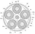
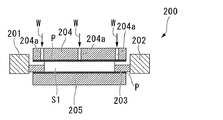
研磨装置200は、図28及び図29に示すように、サンギア201と、インターナルギア202と、キャリア203とを有している。また、キャリア203の上下には、上定盤204及び下定盤205が配置されている。サンギア201及びインターナルギア202は、共に反時計方向に回転するようになっており、キャリア203を遊星運動させている。すなわち、キャリア203を時計方向に自転させながら、反時計方向に公転させている。
As shown in FIGS. 28 and 29, the
キャリア203は、例えば直径数インチの円板からなり、研磨処理前のウエハS1に比べて十分に薄く形成されたもので、ウエハS1を保持する保持孔203Aを形成したものである。保持孔203Aは、図30に示すように、ウエハS1の形状に対応してその開口が正方形状又は矩形状に形成されたもので、あそびを持ってウエハS1を保持するべく、このウエハS1より一回り大きい正方形状(矩形状)に形成されたものである。なお、本例ではウエハS1の大型化に伴い、キャリア203には保持孔203Aが一つだけ形成されている。
また、このようなキャリア203は、上定盤204と下定盤205との間において所定角度毎に複数個配置されるようになっており、したがって研磨装置200では、1バッチの研磨で複数枚のウエハS1を同時に研磨できるようになっている。
The
Further, a plurality of
上定盤204及び下定盤205には、それぞれ対向面に研磨パッドPが着脱可能に固定されている。そして、キャリア203に保持されたウエハS1を両定盤204、205で上下から挟み込んでいる。この際、上定盤204は、所定の荷重をウエハS1に加えた状態となっている。下定盤205は、キャリア203が公転する方向とは逆方向である反時計方向に回転するようになっている。
また、上定盤204には、図29及び図31に示すように、該上定盤204を貫通して両定盤204、205の間に研磨液Wを供給するための、供給路204aが複数(数十個)形成されている。具体的には、半径raの内側円、半径rbの中間円、半径rcの外側円に沿って所定間隔毎に形成されている。そして、図示しない供給ホースを介して研磨液Wが供給路204aに供給されるようになっている。これにより、両定盤204、205の間に各供給路204aを介して研磨液Wを供給することができ、研磨液Wを利用してウエハS1を研磨することができるようになっている。
On the
In addition, as shown in FIGS. 29 and 31, the
なお、上定盤204に形成された研磨パッドPには、供給路204aを塞がないように開口が形成されている。また、研磨液Wとしては、微小な粒径の研磨剤が混入されたものが使用される。また、ラッピング工程あるいはポリッシング工程を行う場合には、通常、同一の構成ではあるものの、異なる研磨装置200を使用している。ただし、ラッピングを行う場合には、通常、研磨パッドPは上定盤204、下定盤205からそれぞれ外し、使用しない。これは、研磨材(遊離砥粒)によるウエハ表面の微細な破壊により、ラッピングを進行させるためである。
An opening is formed in the polishing pad P formed on the
このように構成された研磨装置200によりラッピング工程を行って、ウエハS1を研磨する場合について簡単に説明する。
まず、上定盤204と下定盤205とを離間させた状態で、下定盤205上に各キャリア203をセットする。また、このようにしてセットした各キャリア203の保持孔203AにそれぞれウエハS1をセットする。このようにしてセット工程を終了した後、上定盤204を下降させてウエハS1の上面に該上定盤204を所定の荷重で押し付け、該ウエハS1を両定盤204、205で挟み込む。
A case where the lapping process is performed by the
First, each
そして、供給路204aを介して両定盤204、205の間に研磨液Wを供給しながら、サンギア201、インターナルギア202を駆動させてキャリア203を自転及び公転させる。また、これと同時に下定盤205を回転させる。これにより、キャリア203に保持されたウエハS1の両面を研磨することができ、ウエハS1の厚みを所定の厚みに仕上げることができる。
しかしながら、前記したウエハの研磨には以下の改善すべき課題がある。
前記ウエハS1については、一枚からの取り個数を増やして量産性を向上するべく、前記したように大型化が進んでいる。一方、圧電振動子の小型化の要求に対応するため、ウエハS1は薄厚化も進んでいる。このように、ウエハS1には大型化、薄厚化が同時に求められていることから、図30に示した形態で研磨加工を行った場合に、特にその角部において割れや欠けといった破損が生じ易くなってしまい、その結果歩留まりが低下してしまう。
However, the polishing of the wafer has the following problems to be improved.
As described above, the size of the wafer S1 is increasing in order to increase the number of wafers taken from one wafer and improve mass productivity. On the other hand, in order to meet the demand for miniaturization of the piezoelectric vibrator, the wafer S1 is also becoming thinner. As described above, the wafer S1 is required to be enlarged and thinned at the same time. Therefore, when the polishing process is performed in the form shown in FIG. As a result, the yield decreases.
ここで、研磨処理時には、通常は図30に示したようにウエハS1の角部をC面取り(面取り加工)し、この角部での割れや欠けを防止している。しかしながら、角部を面取り加工しても、直角よりも大きい角部が形成されるだけで、小さくても依然として角部が存在してしまう。したがって、この角部が研磨加工時にキャリア203の保持孔203Aの内周面に接触すると、点(線)接触になることから、ここに大きな負荷がかかることで、前記したように割れや欠けといった破損が生じ易くなってしまう。
Here, during the polishing process, the corner portion of the wafer S1 is normally chamfered (chamfered) as shown in FIG. 30 to prevent cracks and chips at the corner portion. However, even if the corner portion is chamfered, a corner portion larger than a right angle is formed, and the corner portion still exists even if the corner portion is small. Therefore, when this corner portion comes into contact with the inner peripheral surface of the
すなわち、前記したようにウエハS1は大型化が進められていることから、研磨加工時にキャリア203の保持孔203Aの内周面に衝突したり擦れたりすると、大型化された分、その衝撃(負荷)が大きくなっている。一方、薄厚化が進められていることから、その分、ウエハS1自体が脆くなっている。よって、大きな衝撃(負荷)を受けた際、前述したように特に角部において、割れや欠けといった破損が生じ易くなっているのである。
That is, since the wafer S1 has been increased in size as described above, if the wafer S1 collides with or rubs against the inner peripheral surface of the
なお、ウエハとなる水晶等の圧電体は、これを圧電振動片に加工するうえで、その結晶に基づく所定面に対して決められた角度を有してなる基準面を、ウエハの端面として出しておく必要がある。したがって、ウエハとしては、このような基準面がどこにあるか容易に識別できることも、重要となっている。 In addition, when processing a piezoelectric body such as a crystal serving as a wafer into a piezoelectric vibrating piece, a reference plane having a predetermined angle with respect to a predetermined plane based on the crystal is provided as an end face of the wafer. It is necessary to keep. Therefore, it is important for the wafer to be able to easily identify where such a reference plane is.
本発明は前記課題を解決するためになされたもので、その主目的は、特に研磨工程において、割れや欠けといった破損が生じてしまうのが防止されたウエハと、このウエハを研磨する研磨装置及び研磨方法を提供することである。
また、別の目的としては、ウエハ研磨方法を利用して圧電振動子を製造する圧電振動子の製造方法、該製造方法で製造された圧電振動子、該圧電振動子を有する発振器、電子機器及び電波時計を提供することである。
The present invention has been made to solve the above-mentioned problems, and the main object thereof is a wafer in which damage such as cracking or chipping is prevented, particularly in a polishing process, a polishing apparatus for polishing the wafer, and It is to provide a polishing method.
As another object, a piezoelectric vibrator manufacturing method for manufacturing a piezoelectric vibrator using a wafer polishing method, a piezoelectric vibrator manufactured by the manufacturing method, an oscillator having the piezoelectric vibrator, an electronic device, and It is to provide a radio clock.
本発明は、前記課題を解決するために以下の手段を提供する。
本発明に係るウエハは、圧電振動子の原材料として用いられる略角形状で板状のウエハであって、
略角形状における全ての角部が、曲率を付与する面取り加工によって曲面状に形成され、かつ、前記曲面状の角部は、異なる曲率もしくは同じ曲率で面取り加工された第1曲面部と第2曲面部とを少なくとも有してなり、
前記原材料における結晶方位の基準面が、前記第1曲面部又は前記第2曲面部によって特定されてなることを特徴としている。
The present invention provides the following means in order to solve the above problems.
The wafer according to the present invention is a substantially square plate-shaped wafer used as a raw material of a piezoelectric vibrator,
All the corners in the substantially square shape are formed into a curved surface by chamfering that gives curvature, and the curved corners are chamfered with a different curvature or the same curvature and the second curved surface. And at least a curved surface portion,
A reference plane of crystal orientation in the raw material is specified by the first curved surface portion or the second curved surface portion.
このウエハによれば、その角部が、曲率が付与されて曲面状となっているので、研磨加工する際、円形の開口を有する保持孔を形成したキャリアが用いられることにより、その角部、すなわち曲面部での割れや欠けといった破損が防止されたものとなる。つまり、曲面部となっている角部は、キャリアの保持孔の円形開口の内周面に接触した際、点(線)接触でなくほぼ面接触となることから、局部的に大きな負荷(衝撃)がかかることなく、負荷が分散される。したがって、局部的な大きな負荷によって起こる割れや欠けといった破損が、防止されたものとなる。
また、異なる曲率もしくは同じ曲率の第1曲面部と第2曲面部とを有しているので、特にこれら第1曲面部と第2曲面部とを異なる曲率にし、もしくは、これら第1曲面部及び第2曲面部の曲線部分の長さ、すなわち平面視した際の円弧部分の長さを互いに異なるようにしておけば、これら第1曲面部又は第2曲面部によって原材料における結晶方位の基準面が特定されるようになり、したがって、この基準面がどこにあるか容易に識別可能となる。
According to this wafer, since the corner portion has a curved surface with a curvature, when the carrier is formed with a holding hole having a circular opening, the corner portion, That is, breakage such as cracking or chipping at the curved surface portion is prevented. In other words, the corner portion that is a curved surface portion is not a point (line) contact but a substantially surface contact when contacting the inner peripheral surface of the circular opening of the carrier holding hole. ), And the load is distributed. Therefore, breakage such as cracks and chipping caused by a large local load is prevented.
In addition, since the first curved surface portion and the second curved surface portion having different curvatures or the same curvature are provided, in particular, the first curved surface portion and the second curved surface portion have different curvatures, or these first curved surface portions and If the length of the curved portion of the second curved surface portion, that is, the length of the arc portion when viewed in plan is made different from each other, the reference surface of the crystal orientation in the raw material can be set by the first curved surface portion or the second curved surface portion. Thus, it is possible to easily identify where this reference plane is.
また、本発明に係るウエハは、前記本発明のウエハにおいて、略矩形状であって、隣り合う二つの角部が第1曲面部とされ、他の二つの角部が第2曲面部とされ、前記原材料における結晶方位の基準面が、前記第1曲面部間に形成される面、あるいは前記第2曲面部間に形成される端面であるのが好ましい。
このように構成すれば、前記基準面がより容易に識別可能になる。
Further, the wafer according to the present invention is substantially rectangular in the wafer according to the present invention, and two adjacent corners serve as a first curved surface, and the other two corners serve as a second curved surface. It is preferable that the reference plane of crystal orientation in the raw material is a surface formed between the first curved surface portions or an end surface formed between the second curved surface portions.
With this configuration, the reference plane can be identified more easily.
本発明に係るウエハ研磨装置は、前記ウエハの表裏両面を、研磨液を供給しつつ研磨して、該ウエハの厚みを所定の厚みに調整するウエハ研磨装置であって、
外周縁がギア部とされ、前記ウエハが収納される保持孔が形成された円板状のキャリアと、
前記ギア部を介して前記キャリアに噛合され、該キャリアを自転させながら軸線回りに公転させる遊星歯車機構と、
中心が刳り貫かれた円板状に形成され、前記キャリアの上下に配置されて、前記保持孔に収納された前記ウエハに所定の荷重を加えつつ、該ウエハの両面を挟み込む上定盤及び下定盤と、
前記上定盤と前記下定盤との間に前記研磨液を供給する研磨液供給手段と、を備え、
前記キャリアは、前記保持孔が円形の開口を有してなり、該開口における円形の曲率が、前記ウエハの角部の曲率のうち、最も小さい曲率と同じかそれより小さいことを特徴としている。
The wafer polishing apparatus according to the present invention is a wafer polishing apparatus that polishes both the front and back surfaces of the wafer while supplying a polishing liquid, and adjusts the thickness of the wafer to a predetermined thickness.
A disc-shaped carrier having an outer peripheral edge as a gear portion and a holding hole in which the wafer is stored;
A planetary gear mechanism that meshes with the carrier via the gear portion and revolves around an axis while rotating the carrier;
An upper surface plate and a lower surface plate that are formed in a disk shape with a center penetrated, are arranged above and below the carrier, and sandwich the both surfaces of the wafer while applying a predetermined load to the wafer accommodated in the holding hole. The board,
A polishing liquid supply means for supplying the polishing liquid between the upper surface plate and the lower surface plate,
In the carrier, the holding hole has a circular opening, and the circular curvature in the opening is equal to or smaller than the smallest curvature among the curvatures of the corners of the wafer.
本発明に係るウエハ研磨方法は、外周縁がギア部とされ、ウエハが収納される保持孔が形成された円板状のキャリアと、前記ギア部を介して前記キャリアに噛合され、該キャリアを自転させながら軸線回りに公転させる遊星歯車機構と、中心が刳り貫かれた円板状に形成され、前記キャリアの上下に配置されて、前記保持孔に収納された前記ウエハに所定の荷重を加えつつ、該ウエハの両面を挟み込む上定盤及び下定盤と、前記上定盤と前記下定盤との間に前記研磨液を供給する研磨液供給手段と、を備えるウエハ研磨装置により、前記研磨液供給手段から研磨液を供給しつつ、前記ウエハの表裏両面を研磨して、該ウエハの厚みを所定の厚みに調整する研磨工程を備えたウエハ研磨方法であって、
前記キャリアとして、前記保持孔が円形の開口を有し、該開口における円形の曲率が、前記ウエハの角部の曲率のうち、最も小さい曲率と同じかそれより小さいものを用いることを特徴としている。
In the wafer polishing method according to the present invention, the outer peripheral edge is a gear portion, and a disc-shaped carrier having a holding hole for storing a wafer is engaged with the carrier via the gear portion. A planetary gear mechanism that revolves around the axis while rotating, and a disk-like shape with a center penetrated, and is placed above and below the carrier to apply a predetermined load to the wafer housed in the holding hole The polishing liquid is provided by a wafer polishing apparatus comprising: an upper surface plate and a lower surface plate that sandwich both surfaces of the wafer; and a polishing liquid supply unit that supplies the polishing liquid between the upper surface plate and the lower surface plate. A wafer polishing method comprising a polishing step of polishing the front and back surfaces of the wafer while supplying a polishing liquid from a supply means, and adjusting the thickness of the wafer to a predetermined thickness,
The carrier is characterized in that the holding hole has a circular opening, and the circular curvature in the opening is equal to or smaller than the smallest curvature among the curvatures of the corners of the wafer. .
この発明に係るウエハ研磨装置及びウエハ研磨方法においては、研磨加工対象となるウエハとして、前記のウエハを用意する。また、このウエハを保持するキャリアとして、保持孔が円形の開口を有し、該開口における円形の曲率が、前記ウエハの角部の曲率のうち、最も小さい曲率と同じかそれより小さいものを用意する。そして、研磨工程の前に、下定盤上に前記キャリアをセットするとともに、該キャリアの保持孔に研磨加工対象物である前記ウエハを収納し、ここに保持させておく。
このようにしてキャリア及びウエハをセットしたら、研磨工程を行うべく、まず、上定盤を下降させ、キャリアの保持孔内に収納されたウエハの両面を、上定盤と下定盤とで所定の荷重を加えながら挟み込む。
次いで、研磨液供給手段から研磨液を供給しつつ、両定盤でウエハの両面を研磨加工して、ウエハを所定の厚みに調整する。
In the wafer polishing apparatus and the wafer polishing method according to the present invention, the wafer is prepared as a wafer to be polished. Also, as a carrier for holding the wafer, a holding hole having a circular opening and a circular curvature at the opening equal to or smaller than the smallest curvature among the curvatures of the corners of the wafer is prepared. To do. Before the polishing step, the carrier is set on the lower surface plate, and the wafer as an object to be polished is stored in the holding hole of the carrier and held therein.
After the carrier and wafer are set in this way, in order to perform the polishing process, first, the upper surface plate is lowered, and both surfaces of the wafer accommodated in the holding hole of the carrier are fixed to each other with the upper surface plate and the lower surface plate. Clamp while applying load.
Next, while supplying the polishing liquid from the polishing liquid supply means, both surfaces of the wafer are polished with both surface plates to adjust the wafer to a predetermined thickness.
その際、前述したようにウエハの角部が曲面状となっているので、研磨加工時、キャリアの保持孔の内周面に衝突したり擦れたりしても、保持孔が円形の開口を有しており、該開口における円形の曲率が、前記ウエハの角部の曲率のうち、最も小さい曲率と同じかそれより小さいことにより、ウエハの角部、すなわち曲面部での割れや欠けといった破損を防止することができる。
つまり、曲面部となっている角部は、キャリアの保持孔の円形開口の内周面に接触した際、点(線)接触でなくほぼ面接触となることから、局部的に大きな負荷(衝撃)がかかることなく、負荷が分散される。したがって、局部的な大きな負荷によって起こる割れや欠けといった破損を、防止することができる。
At this time, since the corners of the wafer are curved as described above, the holding hole has a circular opening even if it collides with or rubs against the inner peripheral surface of the carrier holding hole during polishing. The circular curvature at the opening is equal to or smaller than the smallest curvature of the corners of the wafer, so that breakage such as cracks or chippings at the corners of the wafer, that is, curved surfaces, is caused. Can be prevented.
In other words, the corner portion that is a curved surface portion is not a point (line) contact but a substantially surface contact when contacting the inner peripheral surface of the circular opening of the carrier holding hole. ), And the load is distributed. Therefore, it is possible to prevent breakage such as cracking or chipping caused by a large local load.
また、本発明に係るウエハ研磨装置は、前記本発明のウエハ研磨装置において、前記キャリアの保持孔の開口における円形の曲率が、前記ウエハの角部の曲率のうちの最も小さい曲率に対して、100%以下で90%以上の大きさであるのが好ましい。
また、本発明に係るウエハ研磨方法は、前記本発明のウエハ研磨方法において、前記キャリアとして、前記保持孔の開口における円形の曲率が、前記ウエハの角部の曲率のうちの最も小さい曲率に対して、100%以下で90%以上の大きさであるものを用いるのが好ましい。
このように構成すれば、ウエハの角部の曲率が保持孔の内周面の曲率以上となり、かつ、この内周面の曲率に十分に近くなるので、このウエハの曲面部となっている角部が、キャリアの保持孔の内周面に接触した際、より面接触に近くなる。したがって、負荷をより良好に分散させることができ、これによって局部的な大きな負荷による割れや欠けといった破損を確実に防止することができる。
Further, the wafer polishing apparatus according to the present invention is the wafer polishing apparatus of the present invention, wherein the circular curvature at the opening of the holding hole of the carrier is the smallest of the curvatures of the corners of the wafer, The size is preferably 100% or less and 90% or more.
Further, the wafer polishing method according to the present invention is the wafer polishing method according to the present invention, wherein the carrier has a circular curvature at the opening of the holding hole as the smallest curvature among the curvatures of the corners of the wafer. Thus, it is preferable to use a material having a size of 100% or less and 90% or more.
With this configuration, the curvature of the corner portion of the wafer is equal to or greater than the curvature of the inner peripheral surface of the holding hole and sufficiently close to the curvature of the inner peripheral surface. When the portion comes into contact with the inner peripheral surface of the holding hole of the carrier, it becomes closer to surface contact. Therefore, the load can be more favorably distributed, and thereby it is possible to reliably prevent breakage such as cracking or chipping caused by a large local load.
また、本発明に係る圧電振動子の製造方法は、前記本発明のウエハ研磨方法により研磨されたウエハを利用して圧電振動子を一度に複数製造する方法であって、研磨後の前記ウエハをフォトリソ技術によりエッチングして、該ウエハに複数の外形形状をパターニングする外形形成工程と、複数の前記圧電振動片の外表面上に電極膜をパターニングして、所定の電圧が印加されたときに圧電振動片を振動させる励振電極と、引き出し電極を介して励振電極に電気的に接続されるマウント電極と、をそれぞれ形成する電極形成工程と、複数の前記圧電振動片を前記ウエハから切り離して固片化する切断工程と、該切断工程後、固片化された前記圧電振動片の前記マウント電極を、一端側が外部に電気的に接続される外部接続端子の他端側に接合するマウント工程と、該マウント工程後、前記圧電振動片を封止部材により気密封止する封止工程と、を備えていることを特徴としている。 The method for manufacturing a piezoelectric vibrator according to the present invention is a method for manufacturing a plurality of piezoelectric vibrators at a time using the wafer polished by the wafer polishing method of the present invention, wherein the wafer after polishing is manufactured. An outer shape forming step of patterning a plurality of outer shapes on the wafer by etching using a photolithographic technique, and patterning an electrode film on the outer surface of the plurality of piezoelectric vibrating reeds so that a piezoelectric material is applied when a predetermined voltage is applied. An electrode forming step of forming an excitation electrode for vibrating the vibration piece and a mount electrode electrically connected to the excitation electrode via the extraction electrode; and a plurality of the piezoelectric vibration pieces separated from the wafer The cutting electrode to be turned into a solid, and after the cutting step, the mount electrode of the piezo-electric vibrating piece separated into pieces is joined to the other end of the external connection terminal whose one end is electrically connected to the outside. And mounting step, after said mounting step is characterized by comprising a sealing step of hermetically sealing by the sealing member the piezoelectric vibrating piece.
この発明に係る圧電振動子の製造方法においては、ウエハ研磨方法により両面が研磨加工され、所定の厚みに高精度に調整されたウエハをフォトリソ技術によりエッチングして、ウエハに複数の圧電振動片の外形形状をパターニングする外形形成工程を行う。
次いで、複数の圧電振動片の外表面上に電極膜をパターニングして、励振電極、引き出し電極及びマウント電極の各電極をそれぞれ形成する電極形成工程を行う。そして、複数の圧電振動片をウエハから切り離して固片化する切断工程を行う。これにより、所定の厚みに調整されたウエハから、励振電極、引き出し電極及びマウント電極が外表面上に形成された圧電振動片を一度に複数製造することができる。
In the method for manufacturing a piezoelectric vibrator according to the present invention, a wafer having both surfaces polished by a wafer polishing method and precisely adjusted to a predetermined thickness is etched by photolithography, and a plurality of piezoelectric vibrating pieces are formed on the wafer. An outer shape forming step of patterning the outer shape is performed.
Next, an electrode forming process is performed in which the electrode film is patterned on the outer surfaces of the plurality of piezoelectric vibrating reeds to form the excitation electrode, the extraction electrode, and the mount electrode, respectively. Then, a cutting process is performed in which the plurality of piezoelectric vibrating pieces are separated from the wafer and solidified. As a result, a plurality of piezoelectric vibrating reeds in which the excitation electrode, the extraction electrode, and the mount electrode are formed on the outer surface can be manufactured from the wafer adjusted to a predetermined thickness at a time.
次いで、固片化された圧電振動片のマウント電極を、一端側が外部に電気的に接続される外部接続端子の他端側に接続するマウント工程を行う。これにより圧電振動片は、外部接続端子に機械的に支持されると共に電気的に接続された状態となる。そして最後に、マウントされた圧電振動片を封止部材により内部に気密封止する封止工程を行う。その結果、圧電振動片が気密封止された圧電振動子を得ることできる。 Next, a mounting step of connecting the mount electrode of the separated piezoelectric vibrating piece to the other end side of the external connection terminal whose one end side is electrically connected to the outside is performed. Accordingly, the piezoelectric vibrating piece is mechanically supported by the external connection terminal and is electrically connected. Finally, a sealing process is performed in which the mounted piezoelectric vibrating piece is hermetically sealed with a sealing member. As a result, a piezoelectric vibrator in which the piezoelectric vibrating piece is hermetically sealed can be obtained.
このように製造された圧電振動子を作動させる場合には、外部接続端子の一端側に対して所定の電圧を印加する。これにより、外部接続端子、マウント電極及び引き出し電極を介して励振電極に電流を流すことができ、圧電振動片を所定の周波数で振動させることができる。
このような圧電振動子の製造方法によれば、前記のウエハ研磨方法により、割れや欠けといった破損が防止された状態で、良好に研磨されたウエハを利用しているので、製造工程全体で見ると、生産性を改善して歩留まりを向上することができ、したがって生産コストの低減化を図ることができる。
また、前記ウエハは、原材料における結晶方位の基準面がどこにあるか容易に識別可能となっているので、このウエハに圧電振動片の外形形状をパターニングする外形形成工程などにおいて、マスクの位置決めなどが容易になる。
When operating the piezoelectric vibrator manufactured as described above, a predetermined voltage is applied to one end side of the external connection terminal. Accordingly, a current can be passed through the excitation electrode via the external connection terminal, the mount electrode, and the extraction electrode, and the piezoelectric vibrating piece can be vibrated at a predetermined frequency.
According to such a method for manufacturing a piezoelectric vibrator, a wafer that has been polished well is used in a state in which breakage such as cracks and chips are prevented by the above-described wafer polishing method. Thus, the productivity can be improved and the yield can be improved, so that the production cost can be reduced.
In addition, since the wafer can be easily identified where the reference plane of the crystal orientation in the raw material is located, in the outer shape forming process for patterning the outer shape of the piezoelectric vibrating piece on the wafer, mask positioning, etc. It becomes easy.
また、本発明に係る圧電振動子は、前記本発明の圧電振動子の製造方法により製造されたことを特徴としている。
この発明に係る圧電振動子によれば、前述した製造方法により製造されているので、従来のものに比べて、生産コストが低減化されたものとなる。
The piezoelectric vibrator according to the present invention is manufactured by the method for manufacturing a piezoelectric vibrator of the present invention.
Since the piezoelectric vibrator according to the present invention is manufactured by the above-described manufacturing method, the production cost is reduced as compared with the conventional one.
また、本発明に係る発振器は、前記本発明の圧電振動子が、発振子として集積回路に電気的に接続されていることを特徴とするものである。
また、本発明に係る電子機器は、前記本発明の圧電振動子が、計時部に電気的に接続されていることを特徴とするものである。
また、本発明に係る電波時計は、前記本発明の圧電振動子が、フィルタ部に電気的に接続されていることを特徴とするものである。
この発明に係る発振器、電子機器及び電波時計においては、前述した圧電振動子を備えているので、従来のものに比べて生産コストが低減化されたものとなる。
The oscillator according to the present invention is characterized in that the piezoelectric vibrator of the present invention is electrically connected to an integrated circuit as an oscillator.
Moreover, the electronic device according to the present invention is characterized in that the piezoelectric vibrator of the present invention is electrically connected to a timer unit.
The radio-controlled timepiece according to the present invention is characterized in that the piezoelectric vibrator of the present invention is electrically connected to a filter portion.
Since the oscillator, the electronic device, and the radio timepiece according to the present invention include the piezoelectric vibrator described above, the production cost is reduced as compared with the conventional one.
本発明に係るウエハによれば、研磨加工した際の、割れや欠けといった破損が防止されているので、生産性が改善されて歩留まりが向上し、生産コストの低減化が図られたものとなる。また、割れや欠けといった破損が防止されているので、大型化、薄厚化も可能になる。
本発明に係るウエハ研磨装置及びウエハ研磨方法によれば、ウエハの角部、すなわち曲面部での割れや欠けといった破損を防止することができるため、生産性を改善して歩留まりを向上し、生産コストの低減化を図ることができる。
また、本発明に係る圧電振動子の製造方法によれば、前述したウエハ研磨方法で研磨されたウエハを利用するので、製造工程全体で見ると、生産コストの低減化を図ることができる。
また、本発明に係る圧電振動子によれば、前述した製造方法により製造されているので、従来のものに比べて生産コストが低減化されたものとなる。
また、本発明に係る発振器、電子機器及び電波時計によれば、前記圧電振動子を備えているので、従来のものに比べて生産コストが低減化されたものとなる。
According to the wafer according to the present invention, damage such as cracking and chipping is prevented at the time of polishing, so that productivity is improved, yield is improved, and production cost is reduced. . In addition, since breakage such as cracking and chipping is prevented, the size and thickness can be reduced.
According to the wafer polishing apparatus and the wafer polishing method according to the present invention, it is possible to prevent breakage such as cracks and chippings at the corners of the wafer, that is, the curved surfaces, thereby improving productivity and improving yield. Cost can be reduced.
In addition, according to the method for manufacturing a piezoelectric vibrator according to the present invention, since the wafer polished by the above-described wafer polishing method is used, the production cost can be reduced when viewed in the entire manufacturing process.
Moreover, according to the piezoelectric vibrator according to the present invention, since it is manufactured by the manufacturing method described above, the production cost is reduced as compared with the conventional one.
In addition, according to the oscillator, electronic device, and radio timepiece according to the present invention, since the piezoelectric vibrator is provided, the production cost is reduced as compared with the conventional one.
以下、本発明の圧電振動子に係る一実施形態を、図1から図19を参照して説明する。なお、本実施形態では、圧電振動子1として、シリンダパッケージタイプの圧電振動子を例に挙げて説明する。
本実施形態の圧電振動子1は、図1から図4に示すように、圧電振動片2と、該圧電振動片2を内部に収納するケース3と、圧電振動片2をケース3内に密閉させる気密端子であるプラグ4と、を備えている。
Hereinafter, an embodiment of the piezoelectric vibrator of the present invention will be described with reference to FIGS. In this embodiment, a cylinder package type piezoelectric vibrator will be described as an example of the
As shown in FIGS. 1 to 4, the
圧電振動片2は、図2及び図3に示すように、水晶、タンタル酸リチウムやニオブ酸リチウム等の圧電材料から形成された音叉型の振動片であり、所定の電圧が印加されたときに振動するものである。なお、この圧電振動片2は、後述するウエハSから作製されたものである。
この圧電振動片2は、平行に配置された一対の振動腕部10、11と、該一対の振動腕部10、11の基端側を一体的に固定する基部12と、一対の振動腕部10、11の外表面上に形成されて一対の振動腕部10、11を振動させる第1の励振電極13と第2の励振電極14とからなる励振電極15と、第1の励振電極13及び第2の励振電極14に電気的に接続されたマウント電極16、17とを有している。
また、本実施形態の圧電振動片2は、一対の振動腕部10、11の両主面上に、該振動腕部10、11の長手方向Xに沿ってそれぞれ形成された溝部18を備えている。この溝部18は、振動腕部10、11の基端側から略中間付近まで形成されている。
As shown in FIGS. 2 and 3, the piezoelectric vibrating
The piezoelectric vibrating
Further, the piezoelectric vibrating
第1の励振電極13と第2の励振電極14とからなる励振電極15は、一対の振動腕部10、11を互いに接近又は離間する方向に所定の共振周波数で振動させる電極であり、一対の振動腕部10、11の外表面に、それぞれ電気的に切り離された状態でパターニングされて形成されている。具体的には、図4に示すように、第1の励振電極13が、一方の振動腕部10の溝部18上と、他方の振動腕部11の両側面上とに主に形成され、第2の励振電極14が、一方の振動腕部10の両側面上と他方の振動腕部11の溝部18上とに主に形成されている。
The
また、第1の励振電極13及び第2の励振電極14は、図2及び図3に示すように、基部12の両主面上において、それぞれ引き出し電極19、20を介してマウント電極16、17に電気的に接続されている。そして圧電振動片2は、このマウント電極16、17を介して電圧が印加されるようになっている。
なお、前述した励振電極15、マウント電極16、17及び引き出し電極19、20は、例えば、クロム(Cr)、ニッケル(Ni)、アルミニウム(Al)やチタン(Ti)等の導電性膜(電極膜)の被膜により形成されたものである。
Further, as shown in FIGS. 2 and 3, the
The
また、一対の振動腕部10、11の先端には、自身の振動状態を所定の周波数の範囲内で振動するように調整(周波数調整)を行うための重り金属膜21が被膜されている。なお、この重り金属膜21は、周波数を粗く調整する際に使用される粗調膜21aと、微小に調整する際に使用される微調膜21bとに分かれている。これら粗調膜21a及び微調膜21bを利用して周波数調整を行うことで、一対の振動腕部10、11の周波数をデバイスの公称周波数の範囲内に収めることができる。
A
ケース3は、図1に示すように有底円筒状に形成されたもので、圧電振動片2を内部に収納した状態で、プラグ4の後述するステム30の外周に対して圧入され、嵌合固定されたものである。なお、このケース3の圧入は真空雰囲気下で行われており、これによってケース3内の圧電振動片2を囲む空間は、真空に保たれた状態となっている。
The
プラグ4は、ケース3を密閉させるステム30と、該ステム30を貫通するように平行配置され、ステム30を間に挟んで一端側が圧電振動片2をマウント(機械的に接合及び電気的に接続)するインナーリード31aとされ、他端側が外部に電気的に接続されるアウターリード31bとされた2本のリード端子31と、ステム30の内側に充填されてステム30とリード端子31とを固定させる絶縁性の充填材32とを有している。
ステム30は、金属材料で環状に形成されたものである。また、充填材32の材料としては、例えばホウ珪酸ガラスが用いられている。また、リード端子31の表面及びステム30の外周には、それぞれ同材料の図示しないメッキが施されている。
The
The
2本のリード端子31は、ケース3内に突出している部分がインナーリード31aとなり、ケース3外に突出している部分がアウターリード31bとなっている。そして、インナーリード31aとマウント電極16、17とが、導電性のバンプEを介してマウントされている。すなわち、バンプEを介してインナーリード31aとマウント電極16、17とが機械的に接合されていると同時に、電気的に接続されている。その結果、圧電振動片2は、2本のリード端子31にマウントされた状態となっている。
In the two
なお、前述した2本のリード端子31は、一端側(アウターリード31b側)が外部に電気的に接続され、他端側(インナーリード31a側)が圧電振動片2に対してマウントされる外部接続端子として機能する。また、ケース3及びプラグ4は、マウントされた圧電振動片2を内部に気密封止する封止部材5として機能する。
The two
ここで、プラグ4を構成する主要部品の寸法及び材質の一例について述べる。
リード端子31の直径は例えば約0.12mmであり、リード端子31の母材の材質としては、コバール(FeNiCo合金)が慣用されている。また、リード端子31の外表面及びステム30の外周に被膜させるメッキの材質としては、下地金属膜としてはCuが用いられ、仕上金属膜としては、耐熱ハンダメッキ(錫と鉛の合金で、その重量比が1:9)や、銀(Ag)や錫銅合金(SnCu)や金錫合金(AuSn)等が用いられる。
また、ステム30の外周に被膜された金属膜(メッキ層)を介在させながらケース3の内周に真空中で冷間圧接させることにより、ケース3の内部を真空状態で気密封止できるようになっている。
Here, an example of dimensions and materials of the main parts constituting the
The diameter of the
Further, the inside of the
このように構成された圧電振動子1を作動させる場合には、2本のリード端子31のアウターリード31bに対して、所定の駆動電圧を印加する。これにより、インナーリード31a、バンプE、マウント電極16、17及び引き出し電極19、20を介して、第1の励振電極13及び第2の励振電極14からなる励振電極15に電流を流すことができ、一対の振動腕部10、11を接近・離間させる方向に所定の周波数で振動させることができる。そして、この一対の振動腕部10、11の振動を利用して、時刻源、制御信号のタイミング源やリファレンス信号源等として利用することができる。
When the
次に、前述した圧電振動子1の製造方法について以下に説明するが、これに先立ち、圧電振動片2の原材料として用いられる本発明に係るウエハSについて説明する。
図5は、本発明に係るウエハの一実施形態を示す図である。図5においてウエハSは、本発明に係るキャリア41の保持孔41bに保持された状態となっている。このウエハSは、略矩形状の板状体であって、その四つの角部全てが、曲率を付与する面取り加工、すなわちR面取り加工によって曲面状に形成されている。
Next, the manufacturing method of the
FIG. 5 is a view showing an embodiment of a wafer according to the present invention. In FIG. 5, the wafer S is held in the holding
これら四つの角部のうち、長辺方向において隣り合う二つの角部D1、D2は、同じ曲率からなる第1曲面部とされ、他の二つの角部D3、D4は、同じ曲率からなる第2曲面部とされている。これら第1曲面部(角部D1、角部D2)と第2曲面部(角部D3、角部D4)とは、互いに異なる曲率に形成され、もしくは同じ曲率に形成されるようになっており、本実施形態では同じ曲率に形成されている。すなわち、第1曲面部における曲率R1は、第2曲面部における曲率R2と同じかあるいはこれより小さく形成されている。(本実施形態では、曲率R1は曲率R2と同じに形成されている。)
また、本実施形態では、これら第1曲面部と第2曲面部とは同じ曲率を有しているものの、その平面視した際の曲線部分の長さ、すなわち平面視した際の円弧部分の長さは、互いに異なって形成されている。(本実施形態では、第1の曲面部の方が第2の曲面部より長くなっている。)このような構成により、第1曲面部と第2曲面部とは、互いに異なっているのが容易に視認でき、したがってこれら第1曲面部と第2曲面部とを容易に識別できるようになっている。
なお、曲率Rは(1/r;ただし、rは円の半径)によって定義され、したがって第1曲面部における曲率R1は(1/r1)となり、第2曲面部における曲率R2は(1/r2)となっている。そして、R1≦R2、すなわちr1≧r2となっている。
Of these four corners, two corners D1 and D2 adjacent in the long side direction are first curved surfaces having the same curvature, and the other two corners D3 and D4 are first curves having the same curvature. 2 curved surface portions. The first curved surface portion (corner portion D1, corner portion D2) and the second curved surface portion (corner portion D3, corner portion D4) are formed with different curvatures or the same curvature. In this embodiment, the same curvature is formed. That is, the curvature R1 in the first curved surface portion is formed to be the same as or smaller than the curvature R2 in the second curved surface portion. (In this embodiment, the curvature R1 is the same as the curvature R2.)
In the present embodiment, the first curved surface portion and the second curved surface portion have the same curvature, but the length of the curved portion when viewed in plan, that is, the length of the arc portion when viewed in plan. They are formed differently from each other. (In the present embodiment, the first curved surface portion is longer than the second curved surface portion.) With such a configuration, the first curved surface portion and the second curved surface portion are different from each other. The first curved surface portion and the second curved surface portion can be easily identified.
The curvature R is defined by (1 / r; where r is the radius of the circle). Therefore, the curvature R1 at the first curved surface portion is (1 / r1), and the curvature R2 at the second curved surface portion is (1 / r2). ). R1 ≦ R2, that is, r1 ≧ r2.
ここで、ウエハSとなる水晶等の圧電体は、前述したようにこれを圧電振動片に加工するうえで、その結晶に基づく所定面に対して決められた角度を有してなる基準面があり、通常はウエハの端面として出しておく必要がある。そこで、本実施形態のウエハSでは、特に前記第1曲面部間の端面、すなわち、角部D1と角部D2との間の端面が、前記の基準面となっている。 Here, the piezoelectric material such as quartz serving as the wafer S is processed into a piezoelectric vibrating piece as described above, and a reference surface having a predetermined angle with respect to a predetermined surface based on the crystal is formed. In general, it is necessary to leave the wafer as the end face of the wafer. Therefore, in the wafer S of the present embodiment, particularly, the end surface between the first curved surface portions, that is, the end surface between the corner portion D1 and the corner portion D2 is the reference surface.
一方、本発明に係るキャリア41は、外縁をギア部41aとし、内部に保持孔41bを一つ有したもので、前記ウエハSより十分に薄い厚さの環状体からなっている。保持孔41bは、開口形状が円形に形成されたもので、あそびを持ってウエハSを保持するべく、その直径が、ウエハSの最長辺より僅かに大きく形成されたものである。そして、この保持孔41bの開口の曲率R3は、前記ウエハSの角部D1〜D4の曲率(R1、R2)のうち、最も小さい曲率R1と同じかそれより小さくなっている。すなわち、R3≦R1(R2)となっている。
On the other hand, the
このような構成のもとにウエハSは、後述するように前記キャリア41の保持孔41bに保持されて研磨加工された際、角部D1〜D4での割れや欠けといった破損が防止されたものとなる。つまり、曲面部となっている角部D1〜D4は、キャリア41の保持孔41bの円形開口の内周面に接触した際、点(線)接触でなくほぼ面接触となることから、局部的に大きな負荷(衝撃)がかかることなく、負荷が分散される。したがって、局部的な大きな負荷によって起こる割れや欠けといった破損が、防止されたものとなる。
また、第1曲面部間の端面が基準面となっているので、研磨処理後もこの基準面が容易に識別可能になっている。
Under such a configuration, the wafer S is prevented from being damaged such as cracks or chips at the corners D1 to D4 when the wafer S is polished in the holding
Further, since the end surface between the first curved surface portions serves as a reference surface, this reference surface can be easily identified even after the polishing process.
次に、図5に示したウエハSの作製を含む圧電振動子1の製造方法について、図6に示すフローチャートを参照しつつ説明する。
前記ウエハSの作製工程では、まず、原石をR面取り加工すると共に、該原石を切断して所定の厚さのウエハSにする。すなわち、横断面矩形状の角柱状の原石を用意すると共に、X線回析法等により原石の切断角度(カット角)の測定を行う(S1)。詳細には、原石のZ面のX軸回りの角度が指定の角度になるようにX線を用いて測定する。測定後、ベースとなるガラス上に接着剤を用いて原石を固定する。なお、本実施形態では原石として水晶を用い、この水晶における基準面が、形成するウエハの端面となるようにする。
Next, a method for manufacturing the
In the manufacturing process of the wafer S, first, the raw stone is R-chamfered, and the raw stone is cut into a wafer S having a predetermined thickness. That is, a prismatic rough with a rectangular cross section is prepared, and the cutting angle (cut angle) of the rough is measured by an X-ray diffraction method or the like (S1). Specifically, the measurement is performed using X-rays so that the angle around the X axis of the Z surface of the rough stone becomes a specified angle. After the measurement, the rough is fixed on the base glass using an adhesive. In this embodiment, quartz is used as the rough stone, and the reference surface of the quartz is made to be the end face of the wafer to be formed.
続いて、前記原石の角部を研磨によってR面取り加工し、横断面である矩形の四つの角部全てを曲面状にする(S2)。研磨方法としては、原石を回転させ、その角部をスエード等の研磨材に擦らせることで行う。その際、原石の回転軸を中心軸から一方の長辺側にずらして回転させ、研磨することで、この回転軸から遠い長辺側の角部と、近い側の角部とが、同じ曲率となり、かつ、平面視した際の曲線部分の長さ(円弧部分の長さ)が、互いに異なるように研磨し、R面取り加工を行う。ただし、前記回転軸から遠くなり、したがって曲線部分の長さが長くなる側の角部(D1、D2)間の長辺が、前記の基準面となるように、この研磨における回転軸を設定する。 Subsequently, the corners of the rough are subjected to R chamfering by polishing, and all the four corners of the rectangular cross section are curved (S2). As a polishing method, the raw stone is rotated and the corners thereof are rubbed against an abrasive such as suede. At that time, by rotating and rotating the rotation axis of the rough stone from the central axis to one long side, the corner on the long side far from the rotation axis and the corner on the near side have the same curvature. Then, polishing is performed so that the length of the curved portion (the length of the arc portion) when viewed in plan is different from each other, and R-chamfering is performed. However, the rotation axis in this polishing is set so that the long side between the corners (D1, D2) on the side that is far from the rotation axis and thus the length of the curved portion becomes the reference surface. .
次いで、角部についてのR面取り加工を行った原石を、ワイヤーソーのワークテーブルにセットする。そして、測定した前記切断角度に沿って、原石をワイヤーソー(例えば、線径が約160μmの高張力線)を用いて約220μmの厚みに切断し、略矩形状のウエハとする(S3)。
なお、本実施形態では、形成するウエハSの最大長を約95mmとする。また、前記切断の際、ワイヤーソーの送り速度を、毎分40mmから50mmに制御する。さらに、切削液としては、砥粒にラッピングオイルを適量配合した液を使用する。この砥粒としては、平均粒径が約12μm程度の炭化珪素(SiC)が慣用される。なお、切削液については、常温を保つように温度管理する。
Next, the rough ore chamfered on the corner is set on the work table of the wire saw. Then, along the measured cutting angle, the raw stone is cut into a thickness of about 220 μm using a wire saw (for example, a high tensile wire having a wire diameter of about 160 μm) to form a substantially rectangular wafer (S3).
In the present embodiment, the maximum length of the wafer S to be formed is about 95 mm. Further, at the time of the cutting, the feed rate of the wire saw is controlled from 40 mm to 50 mm per minute. Further, as the cutting fluid, a liquid in which an appropriate amount of lapping oil is blended into the abrasive grains is used. As the abrasive grains, silicon carbide (SiC) having an average particle diameter of about 12 μm is commonly used. In addition, about the cutting fluid, temperature control is carried out so that normal temperature may be maintained.
次に、ウエハSの側面研磨を行う(S4)。すなわち、切断したウエハSの1枚毎に外周面を研磨するか、あるいは、複数のウエハSを重ね合わせて接着剤で張り合わせてブロックにした後に、図示しない研磨機で外周の研磨を行う。これにより、外周を滑らかに仕上げて、ウエハSの割れや欠け等の発生を抑制することができる。特に、本実施形態の略矩形状のウエハSの場合では、ウエハSの外形の寸法精度を出すことができる。研磨後に、加熱等により接着剤を溶解させ、1枚毎のウエハSに分離する。そして、分離したウエハSを洗浄液中で超音波洗浄して、接着剤を完全に除去する。 Next, side polishing of the wafer S is performed (S4). That is, the outer peripheral surface of each of the cut wafers S is polished, or a plurality of wafers S are overlapped and bonded with an adhesive to form a block, and then the outer periphery is polished by a polishing machine (not shown). As a result, the outer periphery can be finished smoothly, and the occurrence of cracks, chips, etc. of the wafer S can be suppressed. In particular, in the case of the substantially rectangular wafer S of the present embodiment, the dimensional accuracy of the outer shape of the wafer S can be obtained. After polishing, the adhesive is dissolved by heating or the like and separated into wafers S for each sheet. Then, the separated wafer S is ultrasonically cleaned in a cleaning liquid to completely remove the adhesive.
次いで、図7に示すウエハ研磨装置40を用い、側面研磨されたウエハSの両面をラッピング(粗加工)し、所望の厚さにまで研磨する(S5)。ここで、前記ウエハ研磨装置40について詳しく説明する。なお、このウエハ研磨装置40は、図28、図29、図31に示した従来の研磨装置と基本構成は同じであり、異なるところは、図30に示したキャリア203に代えて、図5に示したキャリア41を用いる点である。
Next, using the
このウエハ研磨装置40は、図7、図8に示すように、研磨液Wを供給しながらウエハSの両面を研磨し、該ウエハSの厚みを所定の厚みに調整する装置であって、キャリア41と、遊星歯車機構42と、上定盤43と、下定盤44と、研磨液供給手段45と、を備えて構成されている。
キャリア41は、図5に示したように、外縁をギア部41aとし、内部に保持孔41bを一つ有したもので、保持孔41bの円形開口の曲率R3が、前記ウエハSの角部D1〜D4の曲率(R1、R2)のうち、最も小さい曲率R1(R2)と同じかそれより小さく形成されたものである。具体的には、前記保持孔41bの曲率R3は、前記ウエハSの曲率R1(R2)に対して、100%以下で90%以上の大きさに形成されている。
なお、本実施形態では、図9に示すように、ウエハ研磨装置40が前記構成のキャリア41を5枚備えているものとして説明する。
As shown in FIGS. 7 and 8, the
As shown in FIG. 5, the
In the present embodiment, as shown in FIG. 9, the
前記ウエハ研磨装置40においては、図9に示すように、前記5枚のキャリア41が軸線Lを中心として放射状に所定角度間隔で配置されている。また、前記軸線Lに沿ってシャフト50が配置されており、該シャフト50にはサンギア51が固定されている。また、5枚のキャリア41の周囲を取り囲むように、リング状に形成されたインターナルギア52が配置されている。そして、5枚のキャリア41は、サンギア51及びインターナルギア52に対してギア部41aが噛合した状態で配置されている。
In the
これらサンギア51及びインターナルギア52は、図示しない駆動源により共に反時計方向に回転するようになっている。この際、サンギア51及びインターナルギア52の回転速度は、それぞれ別個の速度で回転するように調整されている。これにより、各キャリア41は、時計方向に自転しながら、軸線Lを中心に反時計方向に公転するようになっている。つまり、サンギア51及びインターナルギア52は、ギア部41aを介してキャリア41に噛合され、該キャリア41を自転させながら軸線L回りに公転させる前記遊星歯車機構42として機能する。
Both the
上定盤43及び下定盤44は、図7、図8、図9に示すように、共に中心が刳り貫かれた円板状(リング状)に形成されており、キャリア41の上下に配置されている。下定盤44は、回転テーブル53上に固定されており、回転テーブル53と共に軸線Lを中心としてキャリア41の公転方向とは反対方向(時計方向)に回転するようになっている。また、上定盤43は、図7に示すようにポール54に沿って上下に移動可能とされており、下定盤44との距離を自在に調整できるようになっている。これにより、キャリア41に形成された保持孔41bにウエハSを収納し、あるいはこれらから取り出したり、キャリア41に収納保持したウエハSに所定の荷重を加えながら、該ウエハSを両定盤で挟み込んだりすることができるようになっている。
As shown in FIGS. 7, 8, and 9, the
両定盤43、44は、キャリア41の一部を両定盤43、44の内周面及び外周面から外側に飛び出させ、露出させるサイズに形成されている。そのため、自転及び公転するキャリア41は、図9に示すように、サンギア51側の一部及びインターナルギア52側の一部が常に露出するようになっている。なお、図9では、下定盤44だけ図示しているが、上定盤43も下定盤44と同じサイズである。
Both the
また、上定盤43の上方には、図7に示すように、パウダーリング55が固定されたリングプレート56が配置されており、該リングプレート56の下面に前記ポール54が固定されている。パウダーリング55には、環状の溝部55aが形成されており、パウダーリング55の上方に配置された供給バルブ57から吐出された研磨液Wを内部に貯留できるようになっている。
また、リングプレート56には、複数のパウダーホース(供給ホース)58の基端側が固定されている。この際、各パウダーホース58は、溝部55a内に連通した状態で固定されている。これにより、溝部55a内に一旦貯留された研磨液Wは、溝部55aからパウダーホース58内に流れ、パウダーホース58の先端に向かって流れるようになっている。
Further, as shown in FIG. 7, a
Further, the base end side of a plurality of powder hoses (supply hoses) 58 is fixed to the
これらパウダーホース58は、その先端が、上定盤43を貫通して形成された供給路(図示せず)に接続固定されている。供給路は、図31に示したように、半径raの内側円、半径rbの中間円、半径rcの外側円に沿って所定間隔毎に形成された貫通孔からなっている。これにより、パウダーホース58から供給された研磨液Wは、各供給路を介して両定盤43、44の間に供給されるようになっている。
The tip ends of these
また、図7に示すように下定盤44の下方には、研磨後に流れてきた研磨液Wを受け取る回収パン61と、回収パン61で受け取られて集められた研磨液Wを貯める研磨液槽62とが配置されている。研磨液槽62には、内部に溜まった研磨液Wを攪拌すると共に、研磨液Wを汲み上げて循環ホース63に循環させるポンプ64が設けられている。そして、循環ホース63は、供給バルブ57に接続された分配器65に接続されている。これにより、回収した研磨液Wを再度供給バルブ57に戻し、パウダーリング55の溝部55a内に供給できるようになっている。
Further, as shown in FIG. 7, below the
なお、前述したパウダーリング55、リングプレート56、供給バルブ57、パウダーホース58、回収パン61、研磨液槽62、循環ホース63、ポンプ64及び分配器65は、上定盤43の供給路を介してこの上定盤43と下定盤44との間に研磨液Wを供給する、前記研磨液供給手段45として機能する。また、このうち、回収パン61、研磨液槽62、循環ホース63、ポンプ64及び分配器65は、供給した研磨液Wを回収すると共に、回収した研磨液Wを循環させて再度両定盤43、44の間に供給する研磨液回収手段66として機能する。
The
また、回収パン61には、フィルタ67が設けられており、回収した研磨液Wに含まれるウエハSの研磨加工粉を除去している。これにより、常に清浄な研磨液Wを両定盤43、44の間に供給し続けることができるようになっている。
なお、前述した研磨液Wは、研磨材(砥粒)が含有された液である。研磨材(砥粒)としては、このラッピングの際には炭化珪素(SiC)が慣用され、平均砥粒が6μmから9μm程度のより粒径の細かいものが使用される。
また、前記の両定盤43、44には、後述するポリッシング工程を行うときとは異なり、研磨パッドPを取り付けることなく外しておき、これを使用せずにラッピング(研磨)を行う。
Further, the
The above-described polishing liquid W is a liquid containing an abrasive (abrasive grains). As the abrasive (abrasive grain), silicon carbide (SiC) is commonly used in the lapping, and a finer one having an average abrasive grain size of about 6 μm to 9 μm is used.
Further, unlike the case where the polishing process described later is performed, the both
このように構成されたウエハ研磨装置40を利用してウエハ研磨を行い、前記ラッピングを行う(S5)。本実施形態のウエハ研磨方法は、図5に示したキャリア41を用いてこれを下定盤44上にセットし、その後遊星歯車機構42によりキャリア41を自転及び公転させて、ウエハSの両面を上定盤43及び下定盤44で研磨する研磨工程を、備えた方法である。この研磨工程について、以下に説明する。
Wafer polishing is performed using the
まず、上定盤43を下定盤44から離間するようにポール54に沿って上方に移動させた後、キャリア41の保持孔41b内にウエハSを収納する。ウエハSの収納後、ポール54に沿って上定盤43を下降させ、保持孔41b内に収納されたウエハSの両面を上定盤43と下定盤44とで所定の荷重を加えながら挟み込む。これにより、ウエハSは、両定盤43、44の表面に挟み込まれた状態となる。
First, after the
次いで、ウエハ研磨処理を行う。すなわち、研磨液供給手段45によって研磨液Wを供給しつつ、これら両定盤43、44によってウエハSの両面を研磨加工し、ウエハSを所定の厚みに調整する。具体的には、研磨液供給手段45によって上定盤43と下定盤44との間に研磨液Wを供給すると同時に、遊星歯車機構42を駆動させてキャリア41を自転させながら、両定盤43、44の中心を貫く軸線L回りに公転させる。ただし、研磨液Wの供給と遊星歯車機構42の作動とを同時にすることなく、研磨液Wの供給を行った後に遊星歯車機構42を駆動させても構わない。また、遊星歯車機構42の駆動と同時に、下定盤44をキャリア41の公転方向と反対方向に回転させる。
Next, a wafer polishing process is performed. That is, while supplying the polishing liquid W by the polishing liquid supply means 45, both surfaces of the wafer S are polished by the both
研磨液供給手段45によって研磨液Wを供給するには、ポンプ64を作動させる。ポンプ64を作動させると、研磨液Wは、図7に示すように研磨液槽62の中で十分に撹拌された後に汲み上げられ、循環ホース63内に送られる。そして、循環ホース63内を通過した後、研磨液Wは分配器65に送られ、該分配器65で分流されてパウダーリング55内の溝部55a内に送られる。溝部55a内に送られた研磨液Wは、該溝部55a内に貯留されると共に、各パウダーホース58に流れ込む。パウダーホース58を流れた研磨液Wは、上定盤43の供給路を介してこの上定盤43と下定盤44との間に流れ込む。これにより、研磨液Wはその一部がキャリア41の上面に流れ落ち、残部が下定盤44上に流れ落ちる。したがって、ウエハSと両定盤43、44との間に研磨に必要な量の研磨液Wが安定して供給される。
In order to supply the polishing liquid W by the polishing liquid supply means 45, the
このようにしてラッピングを行うと、ウエハSの角部D1〜D4が曲面状となっているので、研磨加工時、キャリア41の保持孔41bの内周面に衝突したり擦れたりしても、保持孔41bが円形の開口を有しており、該開口における円形の曲率R3が、前記ウエハSの角部D1〜D4の曲率R1、R2のうち、最も小さい曲率R1(R2)と同じかそれより小さいことにより、ウエハSの角部D1〜D4、すなわち曲面部での割れや欠けといった破損が防止される。
つまり、曲面部となっている角部D1〜D4は、キャリア41の保持孔41bの円形開口の内周面に接触した際、点(線)接触でなくほぼ面接触となることから、局部的に大きな負荷(衝撃)がかかることなく、負荷が分散される。したがって、局部的な大きな負荷によって起こる割れや欠けといった破損が防止される。よって、特にこのラッピング工程では、ウエハSの角部D1〜D4での破損を防止できるため、生産性を改善して歩留まりを向上し、生産コストの低減化を図ることができる。
また、第1曲面部間、すなわち角部D1、D2間の端面が基準面となっているので、ラッピング後もこの基準面が容易に識別可能になっている。
When lapping is performed in this manner, the corners D1 to D4 of the wafer S are curved, so that during polishing, even if they collide or rub against the inner peripheral surface of the holding
That is, when the corners D1 to D4 that are curved portions contact the inner peripheral surface of the circular opening of the holding
Further, since the end surface between the first curved surface portions, that is, the end surfaces between the corner portions D1 and D2, serves as a reference surface, the reference surface can be easily identified even after lapping.
なお、本実施形態では、ウエハSを研磨する際に、下定盤44をキャリア41の公転方向とは反対方向に向けて回転させているので、下定盤44とウエハSとの抵抗を増大でき、より効率良くウエハSを研磨することができる。
また、両定盤43、44の間に供給された研磨液Wは、最終的には図7に示すように、回収パン61によって回収される。そして、回収パン61によって回収された研磨液W及び研磨加工粉は、フィルタ67を通過した後、研磨液槽62に溜まる。フィルタ67を通過する際に、研磨加工粉は除去されるため、研磨液槽62には清浄な研磨液Wだけが溜まるようになる。そして、回収された研磨液Wは、再度ポンプ64によって送り出され、再使用される。
In this embodiment, when polishing the wafer S, the
Further, the polishing liquid W supplied between the two
このように、一度供給した研磨液Wを廃棄して無駄にするのではなく、再度有効利用できるので、研磨液Wに費やすコストの低減化を図ることができる。しかも、フィルタ67を利用して研磨加工粉を除去できるので、常に清浄な研磨液Wだけを安定して供給し続けることができ、高精度な研磨を行うことができる。
In this way, since the polishing liquid W once supplied is not discarded and wasted, but can be used again effectively, the cost spent on the polishing liquid W can be reduced. In addition, since the polishing powder can be removed using the
このようにしてラッピングが終了したら、ウエハSを洗浄する(S6)。すなわち、ウエハSを図示しないバスケットに収納すると共に、バスケットごと洗浄液に漬浸する。そして、超音波洗浄と純水洗浄とを繰り返し行う。また、同時に酸洗浄とアルカリ洗浄とを組み合わせて行う。そして、ウエハSに付着している砥粒を除去した後、純水によるすすぎ洗浄を行う。その後、スピン乾燥機により脱水及び乾燥を行う。 When lapping is completed in this way, the wafer S is cleaned (S6). That is, the wafer S is stored in a basket (not shown) and immersed in the cleaning liquid together with the basket. Then, ultrasonic cleaning and pure water cleaning are repeated. At the same time, acid cleaning and alkali cleaning are combined. Then, after removing the abrasive grains adhering to the wafer S, rinsing with pure water is performed. Thereafter, dehydration and drying are performed by a spin dryer.
次いで、ラッピングによってウエハSの表面に生じた加工変質層を除去する第1のエッチングを行う(S7)。この工程は、ラッピングを行った際に用いた砥粒が加工変質層に食い込んでいるので、ウエハSの両面を約10μm程度フッ酸系の溶液によりエッチングして加工変質層を除去する工程である。詳細には、ウエハSをバスケットに収納した後、所定の時間の間、バスケットごとフッ酸系の溶液であるエッチング液に漬浸する。なおこの間、バスケットをゆっくり上下に揺動させて、ウエハSの厚みにムラが生じてしまうことを防止することが好ましい。そして、所定の時間が経過した後、バスケットをエッチング液から取り出すと共に、純水に漬浸させて十分にエッチング液を取り去る。 Next, first etching is performed to remove a work-affected layer generated on the surface of the wafer S by lapping (S7). This process is a process of removing the work-affected layer by etching both surfaces of the wafer S with a hydrofluoric acid solution of about 10 μm because the abrasive grains used in lapping have bitten into the work-affected layer. . Specifically, after the wafer S is stored in the basket, the entire basket is immersed in an etching solution that is a hydrofluoric acid solution for a predetermined time. During this time, it is preferable to prevent the unevenness in the thickness of the wafer S by slowly swinging the basket up and down. Then, after a predetermined time has elapsed, the basket is taken out of the etching solution and immersed in pure water to sufficiently remove the etching solution.
次いで、ウエハSを乾燥させた後、ウエハSの両面を鏡面研磨して、最終的に厚みを所定の厚みに仕上げて調整するポリッシングを行う(S8)。このポリッシングは、図7に示すウエハ研磨装置40を利用して行うが、先のラッピング時とは異なり、下定盤44の上面、および上定盤43の下面にそれぞれ研磨パッド(図示せず)を接着しておき、その状態で研磨を行う。ウエハSを直接両定盤43、44で挟み込むことなく、研磨パッドを介してウエハSの両面を挟み込み、研磨するのである。
Next, after the wafer S is dried, polishing is performed to mirror-polish both surfaces of the wafer S and finally adjust the thickness to a predetermined thickness (S8). This polishing is performed using the
また、ウエハSを保持するキャリアに関しては、前記ラッピング時と同様に、円形開口の保持孔41bを有してなる、図5に示したキャリア41が用いられる。ただし、このポリッシングに用いるキャリア41としては、その厚さについては研磨対象となるウエハSに対応して、ラッピングに用いるものに比べて厚さが薄いものを用いる。
また、研磨液Wについては、研磨材が含有された液が用いられ、研磨材としては、一般的に酸化セリウム(CeO2)が慣用される。したがって、研磨液Wとしては、例えば酸化セリウムと防錆材と水とからなるスラリーが用いられる。
さらに、ウエハ研磨装置40の動作については、前記ラッピング時と同様にして行う。
As for the carrier for holding the wafer S, the
As the polishing liquid W, a liquid containing an abrasive is used, and cerium oxide (CeO 2 ) is generally used as the abrasive. Therefore, as the polishing liquid W, for example, a slurry made of cerium oxide, a rust preventive material, and water is used.
Further, the operation of the
以上によりポリッシングが終了し、所定の厚さに高精度に仕上げされたウエハSを得ることができる。
このようにしてポリッシングを行っても、前記ラッピング時と同様にウエハSの角部D1〜D4が曲面状となっているので、これらウエハSの角部D1〜D4での割れや欠けといった破損が防止される。よって、このポリッシング工程でも、ウエハSの角部D1〜D4での破損を防止できるため、生産性を改善して歩留まりを向上し、生産コストの低減化を図ることができる。
また、第1曲面部間、すなわち角部D1、D2間の端面が基準面となっているので、ポリッシング後もこの基準面が容易に識別可能になっている。
Thus, the polishing is completed, and the wafer S finished to a predetermined thickness with high accuracy can be obtained.
Even when polishing is performed in this manner, the corners D1 to D4 of the wafer S are curved as in the case of the lapping, so that the corners D1 to D4 of the wafer S are broken or broken. Is prevented. Therefore, even in this polishing step, damage at the corners D1 to D4 of the wafer S can be prevented, so that productivity can be improved, yield can be improved, and production cost can be reduced.
Further, since the end surface between the first curved surface portions, that is, the end surfaces between the corner portions D1 and D2, serves as a reference surface, the reference surface can be easily identified even after polishing.
次いで、ポリッシング終了後、再び洗浄を行う(S9)。すなわち、ウエハSをバスケットに収納した後、超音波洗浄と純水洗浄とを繰り返し行って洗浄を行う。なお、ポリッシングが終了したウエハSは、次工程に移行するまでの間、純水等に漬浸した状態で保管することが好ましい。 Next, after the polishing is completed, cleaning is performed again (S9). That is, after the wafer S is stored in the basket, cleaning is performed by repeatedly performing ultrasonic cleaning and pure water cleaning. The wafer S that has been polished is preferably stored soaked in pure water or the like until the next process is started.
次いで、ポリッシングによってウエハSの表面に生じたダメージ層や何らかの付着物等を除去する第2のエッチングを行う(S10)。詳細には、ウエハSをバスケットに収納した後、所定の時間の間、バスケットごとフッ酸系の溶液であるエッチング液に漬浸してエッチングを行う。
次いで、ウエハSをバスケットに収納した後、純水や60℃程度の温度に加熱した温純水や超純水にバスケットを漬浸して、ウエハSの洗浄を行う(S11)。洗浄した後、ウエハSをスピン乾燥機等で脱水する。脱水後、真空中でウエハSを加熱して、吸着した水分を脱利させて乾燥させる。なお、乾燥後は、窒素を封入したデシケータ中にウエハSを保管するのが好ましい。
Next, second etching is performed to remove a damaged layer or some deposits generated on the surface of the wafer S by polishing (S10). More specifically, after the wafer S is stored in the basket, the entire basket is immersed in an etching solution that is a hydrofluoric acid solution for a predetermined time.
Next, after the wafer S is stored in the basket, the wafer S is cleaned by immersing the basket in pure water, warm pure water heated to a temperature of about 60 ° C. or ultrapure water (S11). After cleaning, the wafer S is dehydrated with a spin dryer or the like. After dehydration, the wafer S is heated in vacuum to desorb the adsorbed moisture and dry. After drying, it is preferable to store the wafer S in a desiccator filled with nitrogen.
次に、前述したように研磨されたウエハSを利用して、圧電振動子1を一度に複数製造する製造方法について、図10及び図11に示すフローチャートを参照して説明する。
本実施形態の圧電振動子1の製造方法は、外形形成工程と、電極形成工程と、切断工程と、マウント工程と、封止工程とを順次行って、製造する方法である。これら各工程について、以下に詳細に説明する。
Next, a manufacturing method for manufacturing a plurality of
The method for manufacturing the
まず、研磨後のウエハSをフォトリソ技術によりエッチングして、複数の圧電振動片2の外形形状をパターニングする外形形成工程を行う(S20)。この工程について、具体的に説明する。
始めに、ポリッシングが終了したウエハSを準備(S21)した後、図12に示すようにウエハSの両面にエッチング保護膜70をそれぞれ成膜する(S22)。このエッチング保護膜70としては、例えば、クロム(Cr)を数μm成膜する。次いで、エッチング保護膜70上に図示しないフォトレジスト膜を、フォトリソグラフィ技術によってパターニングする。この際、圧電振動片2の周囲を囲むようにパターニングする。そして、このフォトレジスト膜をマスクとしてエッチング加工を行い、マスクされていないエッチング保護膜70を選択的に除去する。
なお、前記ウエハSは、結晶方位についての基準面が容易に識別可能となっているので、前記パターニングを行う際、マスクの位置決めなどが容易になっている。
First, the polished wafer S is etched by a photolithographic technique to perform an outer shape forming step of patterning the outer shapes of the plurality of piezoelectric vibrating reeds 2 (S20). This step will be specifically described.
First, after the polishing finished wafer S (S21), an
Since the wafer S can easily identify the reference plane for the crystal orientation, positioning of the mask and the like is facilitated when the patterning is performed.
そして、エッチング加工後にフォトレジスト膜を除去する。これにより、図13及び図14に示すように、エッチング保護膜70を前述した形状にパターニングすることができる(S23)。つまり、圧電振動片2の外形形状、すなわち、一対の振動腕部10、11及び基部12の外形形状に沿ってパターニングすることができる。またこの際、複数の圧電振動片2の数だけパターニングを行う。なお、図14から図19は、図13に示す切断線C−C線に沿った矢視断面を示す図である。
Then, the photoresist film is removed after the etching process. Thereby, as shown in FIG.13 and FIG.14, the etching
次いで、パターニングされたエッチング保護膜70をマスクとして、ウエハSの両面をそれぞれエッチング加工する(S24)。これにより、図15に示すように、エッチング保護膜70でマスクされていない領域を選択的に除去して、圧電振動片2の外形形状を形作ることができる。この時点で、外形形成工程が終了する。なお、圧電振動片2は、後に行う切断工程を行うまで、図示しない連結部を介してウエハSに連結された状態となっている。
Next, both surfaces of the wafer S are etched using the patterned etching
次に、本実施形態では、電極形成工程を行う前に一対の振動腕部10、11に溝部18を形成する溝部形成工程を行う(S30)。この工程について、具体的に説明する。
まず、図16に示すように、エッチング保護膜70上にフォトレジスト膜71をスプレー塗布等により成膜する(S31)。そして、このフォトレジスト膜71を、フォトリソグラフィ技術によってパターニングする。この際、図17に示すように、溝部18の領域を空けた状態で圧電振動片2の外形形状に沿ってパターニングする(S32)。そして、パターニングされたフォトレジスト膜71をマスクとしてエッチング加工を行い、マスクされていないエッチング保護膜70を選択的に除去する(S33)。そして、エッチング加工後にフォトレジスト膜71を除去する。これにより、図18に示すように、既にパターニングされたエッチング保護膜70を、溝部18の領域を空けた状態でさらにパターニングすることができる。
Next, in this embodiment, before performing an electrode formation process, the groove part formation process which forms the
First, as shown in FIG. 16, a
次いで、この再度パターニングされたエッチング保護膜70をマスクとして、ウエハSをエッチング加工(S34)した後、マスクとしていたエッチング保護膜70を除去する(S35)。これにより、図19に示すように、一対の振動腕部10、11に溝部18を形成することができる。この時点で、溝部形成工程が終了する。
Next, the wafer S is etched (S34) using the re-patterned etching
次に、複数の圧電振動片2の外表面上に図示しない電極膜を成膜すると共に、パターニングを行って、励振電極15、引き出し電極19、20、マウント電極16、17をそれぞれ形成する電極形成工程を行う(S40)。また、これと同時に、同様の方法により重り金属膜21を形成する(S41)。
次いで、ウエハSと圧電振動片2とを連結していた連結部を切断して、複数の圧電振動片2をウエハSから切り離して固片化する切断工程を行う(S42)。これにより、所定の厚みに調整されたウエハSから、励振電極15、引き出し電極19、20及びマウント電極16、17の各電極が形成された圧電振動片2を一度に複数製造することができる。
Next, an electrode film (not shown) is formed on the outer surface of the plurality of piezoelectric vibrating
Next, a connecting step that connects the wafer S and the piezoelectric vibrating
次いで、圧電振動片2をマウントする前に、共振周波数の粗調を行う(S43)。これは、重り金属膜21の粗調膜21aにレーザ光を照射して一部を蒸発させ、重量を変化させることで行う。なお、共振周波数をより高精度に調整する微調に関しては後に行う。これについては、後に説明する。
Next, before the piezoelectric vibrating
次に、プラグ4を作製する気密端子作製工程を行う(S50)。具体的には、まず、ステム作製工程によりステム30を作製する(S51)。すなわち、鉄ニッケルコバルト合金や鉄ニッケル合金等の導電性を有する板部材をランス加工した後、複数回の深絞り加工を行って有底の筒部材を形成する。そして、筒部材の底面に開口を形成すると共に、外形抜きを行って筒部材を板部材から切り離すことで、ステム30を作製する。
次いで、ステム30内に、リード端子31及び充填材32をそれぞれセットするセット工程を行う(S52)。まず、作製したステム30を、図示しない専用の治具にセットした後、予めリング状に焼結された充填材32をステム30の内部にセットすると共に、充填材32を貫通するようにリード端子31をセットする。
Next, an airtight terminal manufacturing process for manufacturing the
Next, a setting process for setting the
前記セット工程により、ステム30とリード端子31と充填材32とを組み合わせた後、治具を加熱炉内に入れて1000℃前後の温度雰囲気で充填材32の焼成を行う(S53)。これにより、充填材32とリード端子31との間、充填材32とステム30との間が完全に封着されて、気密に耐えられる構造となる。そして、治具から取り出すことで、プラグ4を得ることができる。この時点で、気密端子作製工程が終了する。
After combining the
次に、リード端子31の外表面及びステム30の外周に同一材料の金属膜を湿式メッキ法で被膜させるメッキ工程を行う(S60)。そのための前処理として、リード端子31の外表面及びステム30の外周を洗浄すると共に、アルカリ溶液で脱脂した後、塩酸及び硫酸の溶液にて酸洗浄を行う。この前処理が終了した後、リード端子31の外表面及びステム30の外周面に下地金属膜を形成する。例えば、Cuメッキ或いはNiメッキを略2μm〜5μmの膜厚で被膜させる。続いて、下地金属膜上に仕上金属膜を形成する。例えば錫や銀等の単一材料の他、耐熱メッキや、錫銅合金、錫ビス膜合金、錫アンチモン合金等を、略8μm〜15μmの膜厚で被膜させる。
このように、下地金属膜及び仕上金属膜からなる金属膜を被膜させることで、インナーリード31aと圧電振動片2との接続を可能にすることができる。また、圧電振動片2の接続だけでなく、ステム30の外周に被膜された金属膜が柔らかく弾性変形する特性を有しているので、ステム30とケース3との冷間圧接を可能にすることができ、気密接合を行うことができる。
Next, a plating process is performed in which a metal film of the same material is coated on the outer surface of the
Thus, the
続いて、金属膜の安定化を図るため、真空雰囲気の炉中でアニーリングを行う(S61)。例えば、170℃の温度で1時間の加熱を行う。これにより、下地金属膜の材料と仕上金属膜の材料との界面に形成される金属間化合物の組成を調整して、ウイスカの発生を抑制することができる。このアニーリングが終了した時点でマウント工程を行うことができる。なお、金属膜を被膜する際に、湿式メッキ法で行った場合を例にしたが、この場合に限られず、例えば、蒸着法や化学気相法等で行っても構わない。 Subsequently, in order to stabilize the metal film, annealing is performed in a vacuum atmosphere furnace (S61). For example, heating is performed at a temperature of 170 ° C. for 1 hour. Thus, whisker generation can be suppressed by adjusting the composition of the intermetallic compound formed at the interface between the material of the base metal film and the material of the finished metal film. The mounting process can be performed when the annealing is completed. In addition, although the case where it carried out by the wet-plating method was taken as an example when coating a metal film, it is not restricted to this case, For example, you may carry out by a vapor deposition method, a chemical vapor phase method, etc.
なお、本実施形態では、アニーリングが終了した後、次に行うマウント工程のためにインナーリード31aの先端に、金等の導電性のバンプEを形成する(S62)。そして、圧電振動片2のマウント電極16、17をインナーリード31aに接合するマウント工程を行う(S63)。具体的には、バンプEを加熱しながら、該バンプEを間に挟んだ状態でインナーリード31aと圧電振動片2とを所定の圧力で重ね合わせる。これにより、バンプEを介してインナーリード31aとマウント電極16、17とを接続することができる。その結果、圧電振動片2をマウントすることができる。すなわち、圧電振動片2は、リード端子31に機械的に支持されると共に、電気的に接続された状態となる。
なお、バンプ接続する際に、加熱・加圧を行ってマウントしたが、超音波を利用してバンプ接続を行っても構わない。
In the present embodiment, after the annealing is completed, a conductive bump E such as gold is formed on the tip of the
In addition, when bump connection is performed by heating and pressurization, the bump connection may be performed using ultrasonic waves.
次に、封止工程を行う前に、前述したマウントによる歪みをなくすために、所定の温度でベーキングを行う(S64)。続いて、圧電振動片2の周波数調整(微調)を行う(S65)。この周波数調整について、具体的に説明すると、全体を真空チャンバーに入れた状態で、アウターリード31b間に電圧を印加して圧電振動片2を振動させる。そして、周波数を計測しながら、レーザにより重り金属膜21の微調膜21bを蒸発させることで、周波数の調整を行う。なお、周波数計測を行うには、アウターリード31bに図示しないプローブの先端を押し付けることで、計測を正確に行うことができる。この周波数調整を行うことで、予め決められた周波数の範囲内に圧電振動片2の周波数を調整することができる。
Next, before performing the sealing step, baking is performed at a predetermined temperature in order to eliminate the distortion caused by the mount described above (S64). Subsequently, the frequency adjustment (fine adjustment) of the piezoelectric vibrating
なお、前記微調及び先に行った粗調の際に、レーザの照射により重り金属膜21を蒸発させることで、周波数調整を行ったが、レーザではなくアルゴンイオンを利用しても構わない。この場合には、アルゴンイオンの照射によりスパッタリングを行い、重り金属膜21を除去することで周波数調整を行う。
Note that the frequency adjustment was performed by evaporating the
最後に、マウントされた圧電振動片2を内部に収納するようにケース3をステム30に圧入し、圧電振動片2を気密封止する封止工程を行う(S66)。具体的に説明すると、真空中で所定の荷重を加えながらケース3をプラグ4のステム30の外周に圧入する。すると、ステム30の外周に形成された金属膜が弾性変形するので、冷間圧接により気密封止することができる。これにより、ケース3内に圧電振動片2を密閉して真空封止することができる。
なお、この工程を行う前に、圧電振動片2、ケース3及びプラグ4を十分に加熱して、表面吸着水分等を脱離させておくことが好ましい。
Finally, the
In addition, before performing this process, it is preferable that the piezoelectric vibrating
そして、ケース3の固定が終了した後、スクリーニングを行う(S67)。このスクリーニングは、周波数や共振抵抗値の安定化を図ると共に、ケース3を圧入した嵌合部に圧縮応力に起因する金属ウイスカが発生してしまうことを抑制するために行うものである。
スクリーニング終了後、内部の電気特性検査を行う(S68)。すなわち、圧電振動片2の共振周波数、共振抵抗値、ドライブレベル特性(共振周波数及び共振抵抗値の励振電力依存性)等を測定してチェックする。また、絶縁抵抗特性等を併せてチェックする。そして、最後に圧電振動子1の外観検査を行って、寸法や品質等を最終的にチェックする。この結果、図1に示す圧電振動子1を製造することができる。
Then, after the
After the screening is completed, an internal electrical characteristic inspection is performed (S68). That is, the resonance frequency, resonance resistance value, drive level characteristic (excitation power dependency of resonance frequency and resonance resistance value), etc. of the piezoelectric vibrating
特に、本実施形態の製造方法によれば、前記ウエハ研磨方法によって破損が防止された状態で良好に研磨されたウエハSを利用しているので、製造工程全体で見ると、生産性を改善して歩留まりを向上することができる。したがって、生産コストの低減化を図ることができる。 In particular, according to the manufacturing method of the present embodiment, the wafer S polished well in a state in which damage is prevented by the wafer polishing method is used, so that productivity is improved in the whole manufacturing process. Yield can be improved. Therefore, the production cost can be reduced.
なお、前記実施形態では、本発明のウエハSとして、図5に示したように略矩形状のものとしたが、角部をR面取り加工してなる略角形状であれば、略三角形状や略五角形状、略六角形状などであってもよい。
また、本発明に係るキャリアについても、図5に示したように、保持孔41bを一つのみ形成したものについて例示したが、ウエハSを同時に複数保持するべく、保持孔41bを複数形成したものであってもよい。
In the embodiment described above, the wafer S of the present invention has a substantially rectangular shape as shown in FIG. 5. However, if the corner portion has a substantially square shape formed by R-chamfering, a substantially triangular shape or It may be a substantially pentagonal shape, a substantially hexagonal shape, or the like.
Further, as shown in FIG. 5, the carrier according to the present invention is illustrated with only one holding
また、前記実施形態では、本発明に係る圧電振動子として、音叉型の圧電振動片2を備えた圧電振動子1を例に挙げて説明したが、本発明はこの圧電振動子1に限定されるものではない。
例えば、図20に示すように、厚み滑り振動片(圧電振動片)81を有する厚み滑り振動子(圧電振動子)80であっても構わない。厚み滑り振動片81は、ウエハSから一定の厚みで板状に形成された圧電板82と、励振電極83、引き出し電極84、マウント電極85とを備えている。圧電板82は、例えば、外形が矩形状に形成されており、両面の略中央部分に励振電極83が対向するように形成されている。圧電板82の端部には、引き出し電極84を介して励振電極83に電気的に接続されたマウント電極85が形成されている。なお、マウント電極85は、一方の励振電極83に接続されたものと、他方の励振電極83に接続されたものとが、圧電板82の両面にそれぞれ形成されている。この際、圧電板82の一方の面に形成されたマウント電極85は、他方の面に形成されたマウント電極85に対して、圧電板82の側面上に形成された側面電極86を介して電気的に接続されている。
In the above embodiment, the
For example, as shown in FIG. 20, a thickness shear vibrator (piezoelectric vibrator) 80 having a thickness shear vibration piece (piezoelectric vibration piece) 81 may be used. The thickness
このように構成された厚み滑り振動子80であっても、前記のウエハ研磨装置40及びウエハ研磨方法によって研磨されたウエハSから厚み滑り振動片81が製造されるので、従来のものに比べて生産コストが低減化されたものとなる。
Even in the thickness-sliding
また、前記実施形態では、圧電振動子の一例として、シリンダパッケージタイプの圧電振動子1を例に挙げて説明したが、この圧電振動子1に限定されるものではない。例えば、図21及び図22に示すように、セラミックパッケージタイプの圧電振動子90でも構わない。
この圧電振動子90は、内部に凹部91aが形成されたベース91と、該ベース91の凹部91a内に収容される圧電振動片2と、圧電振動片2を収容した状態でベース91に固定されるリッド92と、を備えている。
In the embodiment, the cylinder package type
The
ベース91には、ハーメチック封止構造を持つリード93が配置され、その先端にバンプ(図示せず)が設けられている。そして、バンプと圧電振動片2のマウント電極16、17とが機械的及び電気的に接続されている。また、リード93はベース91の底面に露出している。すなわち、このリード93は、一端側が外部に電気的に接続されると共に、他端側がマウント電極16、17に電気的に接続される外部接続端子として機能する。
また、ベース91は、蓋となるリッド92により、真空中で電子ビーム溶接や真空シーム溶接、或いは、低融点ガラスや共晶金属による接合等の各種手段を用いて真空気密封止されている。これにより、圧電振動片2は、内部に気密封止されている。すなわち、ベース91及びリッド92は、圧電振動片2を気密封止する封止部材94として機能する。
A lead 93 having a hermetic sealing structure is disposed on the
The
このように構成された圧電振動子90であっても、前記のウエハ研磨装置40及びウエハ研磨方法によって研磨されたウエハSから圧電振動片2が製造されるので、従来のものに比べて生産コストが低減化されたものとなる。
Even in the
更には、シリンダパッケージタイプの圧電振動子1を、さらにモールド樹脂部101で固めて表面実装型振動子100としても構わない。
この表面実装型振動子100は、図23及び図24に示すように、圧電振動子1と、該圧電振動子1を所定の形状で固定するモールド樹脂部101と、一端側がアウターリード31bに電気的に接続されると共に、他端側がモールド樹脂部101の底面に露出して外部に電気的に接続される外部接続端子102と、を備えている。この外部接続端子102は、銅等の金属材料で断面コ形に形成されている。このように圧電振動子1をモールド樹脂部101で固めることで、回路基板等に安定して取り付けることができるので、より使用し易く、使い易さが向上する。特に、圧電振動子1は従来のものに比べて生産コストが低減化されているので、表面実装型振動子100自体に関しても生産コストが低減化されたものとなる。
Further, the cylinder package type
As shown in FIGS. 23 and 24, the surface-
次に、本発明に係る発振器の一実施形態について、図25を参照しながら説明する。
本実施形態の発振器110は、図25に示すように、圧電振動子1を、集積回路111に電気的に接続された発振子として構成したものである。この発振器110は、コンデンサ等の電子部品112が実装された基板113を備えている。基板113には、発振器用の前記集積回路111が実装されており、この集積回路111の近傍に、圧電振動子1の圧電振動片2が実装されている。これら電子部品112、集積回路111及び圧電振動子1は、図示しない配線パターンによってそれぞれ電気的に接続されている。なお、各構成部品は、図示しない樹脂によりモールドされている。
Next, an embodiment of an oscillator according to the present invention will be described with reference to FIG.
As shown in FIG. 25, the
このように構成された発振器110において、圧電振動子1に電圧を印加すると、該圧電振動子1内の圧電振動片2が振動する。この振動は、圧電振動片2が有する圧電特性により電気信号に変換されて、集積回路111に電気信号として入力される。入力された電気信号は、集積回路111によって各種処理がなされ、周波数信号として出力される。これにより、圧電振動子1が発振子として機能する。
また、集積回路111の構成を、例えば、RTC(リアルタイムクロック)モジュール等を要求に応じて選択的に設定することで、時計用単機能発振器等の他、当該機器や外部機器の動作日や時刻を制御したり、時刻やカレンダー等を提供したりする機能を付加することができる。
In the
In addition, by selectively setting the configuration of the
このような本実施形態の発振器110によれば、従来のものに比べて生産コストが低減化された圧電振動子1を備えているので、発振器110自体に関しても生産コストが低減化されたものとなる。
According to the
次に、本発明に係る電子機器の一実施形態について、図26を参照して説明する。なお電子機器として、前述した圧電振動子1を有する携帯情報機器120を例にして説明する。始めに本実施形態の携帯情報機器120は、例えば、携帯電話に代表されるものであり、従来技術における腕時計を発展、改良したものである。外観は腕時計に類似し、文字盤に相当する部分に液晶ディスプレイを配し、この画面上に現在の時刻等を表示させることができるものである。また、通信機として利用する場合には、手首から外し、バンドの内側部分に内蔵されたスピーカ及びマイクロフォンによって、従来技術の携帯電話と同様の通信を行うことが可能である。しかしながら、従来の携帯電話と比較して、格段に小型化及び軽量化されている。
Next, an embodiment of an electronic apparatus according to the invention will be described with reference to FIG. Note that a
次に、本実施形態の携帯情報機器120の構成について説明する。この携帯情報機器120は、図26に示すように、圧電振動子1と、電力を供給するための電源部121とを備えている。電源部121は、例えば、リチウム二次電池からなっている。この電源部121には、各種制御を行う制御部122と、時刻等のカウントを行う計時部123と、外部との通信を行う通信部124と、各種情報を表示する表示部125と、それぞれの機能部の電圧を検出する電圧検出部126とが並列に接続されている。そして、電源部121によって、各機能部に電力が供給されるようになっている。
Next, the configuration of the
制御部122は、各機能部を制御して音声データの送信及び受信、現在時刻の計測や表示等、システム全体の動作制御を行う。また、制御部122は、予めプログラムが書き込まれたROMと、該ROMに書き込まれたプログラムを読み出して実行するCPUと、該CPUのワークエリアとして使用されるRAM等とを備えている。
The
計時部123は、発振回路、レジスタ回路、カウンタ回路及びインターフェース回路等を内蔵する集積回路と、圧電振動子1とを備えている。圧電振動子1に電圧を印加すると圧電振動片2が振動し、該振動が水晶の有する圧電特性により電気信号に変換されて、発振回路に電気信号として入力される。発振回路の出力は二値化され、レジスタ回路とカウンタ回路とにより計数される。そして、インターフェース回路を介して、制御部122と信号の送受信が行われ、表示部125に、現在時刻や現在日付或いはカレンダー情報等が表示される。
The
通信部124は、従来の携帯電話と同様の機能を有し、無線部127、音声処理部128、切替部129、増幅部130、音声入出力部131、電話番号入力部132、着信音発生部133及び呼制御メモリ部134を備えている。
無線部127は、音声データ等の各種データを、アンテナ135を介して基地局と送受信のやりとりを行う。音声処理部128は、無線部127又は増幅部130から入力された音声信号を符号化及び複号化する。増幅部130は、音声処理部128又は音声入出力部131から入力された信号を、所定のレベルまで増幅する。音声入出力部131は、スピーカやマイクロフォン等からなり、着信音や受話音声を拡声したり、音声を集音したりする。
The
The
また、着信音発生部133は、基地局からの呼び出しに応じて着信音を生成する。切替部129は、着信時に限って、音声処理部128に接続されている増幅部130を着信音発生部133に切り替えることによって、着信音発生部133において生成された着信音が増幅部130を介して音声入出力部131に出力される。
なお、呼制御メモリ部134は、通信の発着呼制御に係るプログラムを格納する。また、電話番号入力部132は、例えば、0から9の番号キー及びその他のキーを備えており、これら番号キー等を押下することにより、通話先の電話番号等が入力される。
In addition, the
Note that the call
電圧検出部126は、電源部121によって制御部122等の各機能部に対して加えられている電圧が、所定の値を下回った場合に、その電圧降下を検出して制御部122に通知する。このときの所定の電圧値は、通信部124を安定して動作させるために必要な最低限の電圧として予め設定されている値であり、例えば、3V程度となる。電圧検出部126から電圧降下の通知を受けた制御部122は、無線部127、音声処理部128、切替部129及び着信音発生部133の動作を禁止する。特に、消費電力の大きな無線部127の動作停止は、必須となる。更に、表示部125に、通信部124が電池残量の不足により使用不能になった旨が表示される。
The
すなわち、電圧検出部126と制御部122とによって、通信部124の動作を禁止し、その旨を表示部125に表示することができる。この表示は、文字メッセージであっても良いが、より直感的な表示として、表示部125の表示面の上部に表示された電話アイコンに、×(バツ)印を付けるようにしても良い。
なお、通信部124の機能に係る部分の電源を、選択的に遮断することができる電源遮断部136を備えることで、通信部124の機能をより確実に停止することができる。
That is, the operation of the
In addition, the function of the
前述したように、本実施形態の携帯情報機器120によれば、従来のものに比べて生産コストが低減化された圧電振動子1を備えているので、携帯情報機器120自体に関しても生産コストが低減化されたものとなる。
As described above, according to the
次に、本発明に係る電波時計の一実施形態について、図27を参照して説明する。
本実施形態の電波時計140は、図27に示すように、フィルタ部141に電気的に接続された圧電振動子1を備えたものであり、時計情報を含む標準の電波を受信して、正確な時刻に自動修正して表示する機能を備えた時計である。
日本国内には、福島県(40kHz)と佐賀県(60kHz)とに、標準の電波を送信する送信所(送信局)があり、それぞれ標準電波を送信している。40kHz若しくは60kHzのような長波は、地表を伝播する性質と、電離層と地表とを反射しながら伝播する性質とを併せもつため、伝播範囲が広く、前述した2つの送信所で日本国内を全て網羅している。
Next, an embodiment of a radio timepiece according to the present invention will be described with reference to FIG.
As shown in FIG. 27, the radio-controlled
In Japan, there are transmitting stations (transmitting stations) that transmit standard radio waves in Fukushima Prefecture (40 kHz) and Saga Prefecture (60 kHz), each transmitting standard radio waves. Long waves such as 40 kHz or 60 kHz have both the property of propagating the ground surface and the property of propagating while reflecting the ionosphere and the ground surface, so the propagation range is wide, and the above two transmitting stations cover all of Japan. doing.
以下、電波時計140の機能的構成について詳細に説明する。
アンテナ142は、40kHz若しくは60kHzの長波の標準電波を受信する。長波の標準電波は、タイムコードと呼ばれる時刻情報を、40kHz若しくは60kHzの搬送波にAM変調をかけたものである。受信された長波の標準電波は、アンプ143によって増幅され、複数の圧電振動子1を有するフィルタ部141によって濾波、同調される。
本実施形態における圧電振動子1は、前記搬送周波数と同一の40kHz及び60kHzの共振周波数を有する水晶振動子部148、149をそれぞれ備えている。
Hereinafter, the functional configuration of the
The
The
更に、濾波された所定周波数の信号は、検波、整流回路144により検波復調される。
続いて、波形整形回路145を介してタイムコードが取り出され、CPU146でカウントされる。CPU146では、現在の年、積算日、曜日、時刻等の情報を読み取る。読み取られた情報は、RTC148に反映され、正確な時刻情報が表示される。
搬送波は、40kHz若しくは60kHzであるから、水晶振動子部148、149は、前述した音叉型の構造を持つ振動子が好適である。
Further, the filtered signal having a predetermined frequency is detected and demodulated by the detection and
Subsequently, the time code is taken out via the
Since the carrier wave is 40 kHz or 60 kHz, the
なお、前述の説明は、日本国内の例で示したが、長波の標準電波の周波数は、海外では異なっている。例えば、ドイツでは77.5KHzの標準電波が用いられている。従って、海外でも対応可能な電波時計140を携帯機器に組み込む場合には、さらに日本の場合とは異なる周波数の圧電振動子1を必要とする。
In addition, although the above-mentioned description was shown in the example in Japan, the frequency of the long standard wave is different overseas. For example, in Germany, a standard radio wave of 77.5 KHz is used. Therefore, when the
前述したように、本実施形態の電波時計140によれば、従来のものに比べて生産コストが低減化された圧電振動子1を備えているので、電波時計140自体に関しても生産コストが低減化されたものとなる。
As described above, according to the radio-controlled
D1、D2、D3、D4…角部、L…軸線、S…ウエハ、W…研磨液、1、90…圧電振動子、2…圧電振動片、5、94…封止部材、15、83…励振電極、16、17、85…マウント電極、19、20、84…引き出し電極、31…リード端子(外部接続端子)、40…ウエハ研磨装置、41…キャリア、41a…キャリアのギア部、41b…キャリアの保持孔、42…遊星歯車機構、43…上定盤、44…下定盤、45…研磨液供給手段、58…パウダーホース、66…研磨液回収手段、67…フィルタ、90…厚み滑り振動片、93…リード(外部接続端子)、80…厚み滑り振動子(圧電振動子)、81…厚み滑り振動片(圧電振動片)、110…発振器、120…携帯情報機器(電子機器)、140…電波時計
D1, D2, D3, D4 ... Corner, L ... Axis, S ... Wafer, W ... Polishing liquid, 1, 90 ... Piezoelectric vibrator, 2 ... Piezoelectric vibrating
Claims (6)
略角形状における全ての角部が、曲率を付与する面取り加工によって曲面状に形成され、かつ、前記曲面状の角部は、異なる曲率で面取り加工された第1曲面部と第2曲面部とを少なくとも有してなり、
前記原材料における結晶方位の基準面が、前記第1曲面部又は前記第2曲面部によって特定されてなることを特徴とするウエハ。 A substantially square plate-shaped wafer used as a raw material for a piezoelectric vibrator,
All corners in a substantially square shape are formed into a curved surface by chamfering to give curvature, and the curved corners are chamfered with different curvatures , a first curved surface portion and a second curved surface portion. Having at least
A wafer characterized in that a reference plane of crystal orientation in the raw material is specified by the first curved surface portion or the second curved surface portion.
略角形状における全ての角部が、曲率を付与する面取り加工によって曲面状に形成され、かつ、前記曲面状の角部は、平面視した際の曲線部分の長さを異ならせて面取り加工された第1曲面部と第2曲面部とを少なくとも有してなり、
前記原材料における結晶方位の基準面が、前記第1曲面部又は前記第2曲面部によって特定されてなることを特徴とするウエハ。 A substantially square plate-shaped wafer used as a raw material for a piezoelectric vibrator,
All corners in a substantially square shape are formed into a curved surface by chamfering that gives curvature, and the curved corners are chamfered by varying the length of the curved portion when viewed in plan. At least a first curved surface portion and a second curved surface portion,
A wafer characterized in that a reference plane of crystal orientation in the raw material is specified by the first curved surface portion or the second curved surface portion.
略矩形状であって、隣り合う二つの角部が第1曲面部とされ、他の二つの角部が第2曲面部とされ、
前記原材料における結晶方位の基準面が、前記第1曲面部間に形成される面、あるいは前記第2曲面部間に形成される端面であることを特徴とするウエハ。 The wafer according to claim 1 or 2 ,
It is a substantially rectangular shape, and the two adjacent corners are the first curved surface part, and the other two corners are the second curved surface part,
A wafer characterized in that a reference plane of crystal orientation in the raw material is a plane formed between the first curved surface portions or an end surface formed between the second curved surface portions.
前記ウエハは、略角形状の板状で、略角形状における全ての角部が、曲率を付与する面取り加工によって曲面状に形成され、かつ、前記曲面状の角部は、異なる曲率で面取り加工された第1曲面部と第2曲面部とを少なくとも有してなり、前記原材料における結晶方位の基準面が、前記第1曲面部又は前記第2曲面部によって特定されてなり、
前記キャリアとして、前記保持孔が円形の開口を有し、該開口における円形の曲率が、前記ウエハの角部の曲率のうち、最も小さい曲率と同じかそれより小さいものを用いることを特徴とするウエハ研磨方法。 A disk-shaped carrier having an outer peripheral edge as a gear portion and a holding hole in which a wafer is accommodated, and a planet that meshes with the carrier via the gear portion and revolves around the axis while rotating the carrier. A gear mechanism, which is formed in a disc shape with the center being punched, is disposed above and below the carrier, and sandwiches both surfaces of the wafer while applying a predetermined load to the wafer accommodated in the holding hole. and a platen and lower platen, using a polishing liquid supply means for supplying the polishing liquid between the upper surface plate and the lower plate, while supplying the polishing liquid from the polishing liquid supply means, said wafer both sides by polishing, the thickness of the wafer to a wafer polishing method comprising a polishing step of adjusting to a predetermined thickness,
The wafer has a substantially square plate shape, and all the corners of the substantially square shape are formed into a curved surface by chamfering to give curvature, and the curved corners are chamfered with different curvatures. The first curved surface portion and the second curved surface portion at least, the reference plane of the crystal orientation in the raw material is specified by the first curved surface portion or the second curved surface portion,
As the carrier, the holding hole has a circular opening, and the circular curvature in the opening is equal to or smaller than the smallest curvature among the curvatures of the corners of the wafer. Wafer polishing method.
前記ウエハは、略角形状の板状で、略角形状における全ての角部が、曲率を付与する面取り加工によって曲面状に形成され、かつ、前記曲面状の角部は、平面視した際の曲線部分の長さを異ならせて面取り加工された第1曲面部と第2曲面部とを少なくとも有してなり、前記原材料における結晶方位の基準面が、前記第1曲面部又は前記第2曲面部によって特定されてなり、
前記キャリアとして、前記保持孔が円形の開口を有し、該開口における円形の曲率が、前記ウエハの角部の曲率のうち、最も小さい曲率と同じかそれより小さいものを用いることを特徴とするウエハ研磨方法。 A disk-shaped carrier having an outer peripheral edge as a gear portion and a holding hole in which a wafer is accommodated, and a planet that meshes with the carrier via the gear portion and revolves around the axis while rotating the carrier. A gear mechanism, which is formed in a disc shape with the center being punched, is disposed above and below the carrier, and sandwiches both surfaces of the wafer while applying a predetermined load to the wafer accommodated in the holding hole. and a platen and lower platen, using a polishing liquid supply means for supplying the polishing liquid between the upper surface plate and the lower plate, while supplying the polishing liquid from the polishing liquid supply means, said wafer both sides by polishing, the thickness of the wafer to a wafer polishing method comprising a polishing step of adjusting to a predetermined thickness,
The wafer is a plate having a substantially square shape, and all corners in the substantially square shape are formed into a curved surface by chamfering that gives curvature, and the corners of the curved surface are in a plan view. It has at least a first curved surface portion and a second curved surface portion that are chamfered by varying the length of the curved portion, and the reference surface of the crystal orientation in the raw material is the first curved surface portion or the second curved surface. Specified by the department,
As the carrier, the holding hole has a circular opening, and the circular curvature in the opening is equal to or smaller than the smallest curvature among the curvatures of the corners of the wafer. Wafer polishing method.
前記キャリアとして、前記保持孔の開口における円形の曲率が、前記ウエハの角部の曲率のうちの最も小さい曲率に対して、100%以下で90%以上の大きさであるものを用いることを特徴とするウエハ研磨方法。 The wafer polishing method according to claim 4 or 5,
A carrier having a circular curvature at the opening of the holding hole of 100% or less and 90% or more with respect to the smallest curvature among the curvatures of the corners of the wafer is used as the carrier. Wafer polishing method .
Priority Applications (5)
| Application Number | Priority Date | Filing Date | Title |
|---|---|---|---|
| JP2008033070A JP5138407B2 (en) | 2008-02-14 | 2008-02-14 | Wafer and wafer polishing method |
| TW98101909A TW201004740A (en) | 2008-02-14 | 2009-01-19 | Wafer, wafer polishing apparatus, wafer polishing method, method of fabricating piezoelectric vibrator, piezoelectric vibrator, oscillator, electronic apparatus and radiowave timepiece |
| US12/361,913 US8063545B2 (en) | 2008-02-14 | 2009-01-29 | Wafer, wafer polishing apparatus, wafer polishing method, method of fabricating piezoelectric vibrator, piezoelectric vibrator, oscillator, electronic apparatus and radiowave timepiece |
| CH00231/09A CH698481B1 (en) | 2008-02-14 | 2009-02-12 | Wafers as the starting material for a piezoelectric vibrator |
| CN200910008256.6A CN101510767B (en) | 2008-02-14 | 2009-02-16 | Wafer and polishing device and method, piezoelectric vibrating piece, method and apparatus for fabricating piezoelectric vibrating piece |
Applications Claiming Priority (1)
| Application Number | Priority Date | Filing Date | Title |
|---|---|---|---|
| JP2008033070A JP5138407B2 (en) | 2008-02-14 | 2008-02-14 | Wafer and wafer polishing method |
Publications (2)
| Publication Number | Publication Date |
|---|---|
| JP2009194631A JP2009194631A (en) | 2009-08-27 |
| JP5138407B2 true JP5138407B2 (en) | 2013-02-06 |
Family
ID=40951459
Family Applications (1)
| Application Number | Title | Priority Date | Filing Date |
|---|---|---|---|
| JP2008033070A Active JP5138407B2 (en) | 2008-02-14 | 2008-02-14 | Wafer and wafer polishing method |
Country Status (5)
| Country | Link |
|---|---|
| US (1) | US8063545B2 (en) |
| JP (1) | JP5138407B2 (en) |
| CN (1) | CN101510767B (en) |
| CH (1) | CH698481B1 (en) |
| TW (1) | TW201004740A (en) |
Families Citing this family (15)
| Publication number | Priority date | Publication date | Assignee | Title |
|---|---|---|---|---|
| JP5485714B2 (en) * | 2010-01-07 | 2014-05-07 | セイコーインスツル株式会社 | Package manufacturing method |
| JP6383164B2 (en) * | 2014-03-25 | 2018-08-29 | エスアイアイ・クリスタルテクノロジー株式会社 | Method for manufacturing piezoelectric vibrating piece |
| KR101660898B1 (en) * | 2014-08-13 | 2016-09-28 | 주식회사 엘지실트론 | Apparatus for supplying slurry and polishing apparatus including the same |
| CN105161397B (en) * | 2015-05-13 | 2019-02-05 | 北京通美晶体技术有限公司 | A kind of abnormity semiconductor wafer, preparation method and wafer supporting pad |
| JP6719178B2 (en) * | 2015-05-22 | 2020-07-08 | エスアイアイ・クリスタルテクノロジー株式会社 | Method of manufacturing piezoelectric vibrating piece and method of manufacturing piezoelectric vibrator |
| JP6610587B2 (en) * | 2017-03-13 | 2019-11-27 | 信越半導体株式会社 | Wafer manufacturing method |
| JP6939876B2 (en) * | 2017-03-30 | 2021-09-22 | 株式会社大真空 | Tuning fork type piezoelectric vibrating piece and tuning fork type piezoelectric vibrator using the tuning fork type piezoelectric vibrating piece |
| US10350726B2 (en) | 2017-06-19 | 2019-07-16 | Taiwan Semiconductor Manufacturing Co., Ltd. | Chemical mechanical polishing system and method |
| CN108858833A (en) * | 2018-08-31 | 2018-11-23 | 江苏英锐半导体有限公司 | A kind of wafer cutting equipment |
| CN110103134A (en) * | 2019-05-14 | 2019-08-09 | 应达利电子股份有限公司 | Wafer processing method |
| CN112792711B (en) * | 2020-12-31 | 2022-05-17 | 武汉风帆电化科技股份有限公司 | Crystal silicon wafer alkali polishing device and polishing process |
| TWI776445B (en) * | 2021-03-30 | 2022-09-01 | 台灣晶技股份有限公司 | Crystal oscillator package structure |
| CN113182971B (en) * | 2021-05-12 | 2022-11-25 | 四川雅吉芯电子科技有限公司 | High-precision edge grinding device for monocrystalline silicon epitaxial wafer |
| CN113878501B (en) * | 2021-09-02 | 2023-12-19 | 宁海县勇昊汽车部件有限公司 | Surface treatment system based on electromagnetic wave monitoring and control method |
| CN114290230B (en) * | 2021-12-31 | 2023-05-05 | 华侨大学 | Device and method for laser-induced plasma-assisted double-sided grinding of transparent material |
Family Cites Families (30)
| Publication number | Priority date | Publication date | Assignee | Title |
|---|---|---|---|---|
| JPS5931247B2 (en) * | 1975-11-18 | 1984-08-01 | シチズン時計株式会社 | Suishiyo Shindoushi |
| JPS5741164A (en) * | 1980-08-12 | 1982-03-08 | Citizen Watch Co Ltd | Dual carrier for lapping |
| JP2608757B2 (en) * | 1988-05-16 | 1997-05-14 | セイコー電子工業株式会社 | Quartz crystal crystal wafer |
| JPH03228568A (en) * | 1990-01-29 | 1991-10-09 | Shin Etsu Chem Co Ltd | Manufacture of extremely thin wafer |
| JPH0460653U (en) * | 1990-09-29 | 1992-05-25 | ||
| JPH0588028U (en) * | 1992-04-24 | 1993-11-26 | シチズン時計株式会社 | Piezoelectric vibrator and container for storing the piezoelectric vibrator |
| JPH08186459A (en) * | 1994-12-28 | 1996-07-16 | Ngk Spark Plug Co Ltd | Manufacture of chip type piezoelectric filter |
| JP3319221B2 (en) * | 1995-06-02 | 2002-08-26 | 松下電器産業株式会社 | Transducer manufacturing method |
| JPH10180623A (en) * | 1996-12-26 | 1998-07-07 | Mitsubishi Materials Shilicon Corp | Lapping device |
| JPH11156707A (en) * | 1997-11-28 | 1999-06-15 | Naoetsu Electronics Co Ltd | Work carrier for grinding device |
| JP3975251B2 (en) * | 1998-12-14 | 2007-09-12 | セイコーエプソン株式会社 | Polishing carrier, surface polishing apparatus and surface polishing method |
| JP3791302B2 (en) * | 2000-05-31 | 2006-06-28 | 株式会社Sumco | Semiconductor wafer polishing method using a double-side polishing apparatus |
| JP2002231845A (en) * | 2001-01-30 | 2002-08-16 | Kyocera Corp | Electronic part storing package |
| JP3528811B2 (en) * | 2001-04-18 | 2004-05-24 | セイコーエプソン株式会社 | Method for forming electrode of piezoelectric vibrating piece, mask for forming electrode of piezoelectric vibrating piece, piezoelectric vibrator, and piezoelectric oscillator |
| JP3977037B2 (en) * | 2001-08-08 | 2007-09-19 | 株式会社荏原製作所 | Quadrilateral substrate polishing equipment |
| JP4120312B2 (en) * | 2001-10-16 | 2008-07-16 | セイコーエプソン株式会社 | Piezoelectric vibrating piece and processing method thereof |
| JP2003318697A (en) * | 2002-04-25 | 2003-11-07 | Seiko Instruments Inc | At-cut quartz resonator |
| DE10260854A1 (en) * | 2002-12-23 | 2004-07-08 | Robert Bosch Gmbh | piezo actuator |
| WO2006046494A1 (en) * | 2004-10-25 | 2006-05-04 | Ngk Insulators, Ltd. | Piezoelectric/electrostrictive device |
| JP2006217497A (en) * | 2005-02-07 | 2006-08-17 | Seiko Instruments Inc | Method for manufacturing crystal oscillating piece, crystal oscillating piece, oscillator, and electronic equipment |
| JP2006262443A (en) * | 2005-02-10 | 2006-09-28 | Seiko Instruments Inc | Piezoelectric vibrator, surface-mounting type piezoelectric vibrator, oscillator, electronic apparatus and wave clock |
| JP2006339896A (en) | 2005-05-31 | 2006-12-14 | Kyocera Kinseki Corp | Method for manufacturing piezoelectric vibrator and piezoelectric vibrator |
| JP4845478B2 (en) * | 2005-10-24 | 2011-12-28 | セイコーインスツル株式会社 | Piezoelectric vibrator, method for manufacturing piezoelectric vibrator, oscillator, electronic device, and radio timepiece |
| JP2007130690A (en) * | 2005-11-08 | 2007-05-31 | Hamai Co Ltd | Carrier for planetary gear type polishing device |
| JP2007158566A (en) * | 2005-12-02 | 2007-06-21 | Epson Toyocom Corp | Piezoelectric vibration chip and piezoelectric device |
| JP2007184810A (en) | 2006-01-10 | 2007-07-19 | Epson Toyocom Corp | Method for manufacturing piezoelectric vibrator |
| JP2007227872A (en) * | 2006-01-27 | 2007-09-06 | Ngk Insulators Ltd | Piezoelectric/electrostrictive actuator |
| JP4812014B2 (en) * | 2006-07-12 | 2011-11-09 | セイコーインスツル株式会社 | Piezoelectric vibrating piece, method for manufacturing piezoelectric vibrating piece, piezoelectric vibrator, oscillator including piezoelectric vibrator, electronic device, and radio timepiece |
| JP2008028590A (en) * | 2006-07-20 | 2008-02-07 | Seiko Instruments Inc | Piezoelectric vibrating-reed and manufacturing method of piezoelectric vibrating-reed, piezoelectric vibrator, oscillator with piezoelectric vibrator, electronic device, and radio clock |
| JP5061694B2 (en) * | 2007-04-05 | 2012-10-31 | 信越半導体株式会社 | Polishing pad manufacturing method, polishing pad, and wafer polishing method |
-
2008
- 2008-02-14 JP JP2008033070A patent/JP5138407B2/en active Active
-
2009
- 2009-01-19 TW TW98101909A patent/TW201004740A/en unknown
- 2009-01-29 US US12/361,913 patent/US8063545B2/en not_active Expired - Fee Related
- 2009-02-12 CH CH00231/09A patent/CH698481B1/en not_active IP Right Cessation
- 2009-02-16 CN CN200910008256.6A patent/CN101510767B/en active Active
Also Published As
| Publication number | Publication date |
|---|---|
| CH698481A2 (en) | 2009-08-14 |
| US20100231088A1 (en) | 2010-09-16 |
| JP2009194631A (en) | 2009-08-27 |
| CN101510767B (en) | 2014-03-26 |
| CH698481B1 (en) | 2013-09-30 |
| TW201004740A (en) | 2010-02-01 |
| US8063545B2 (en) | 2011-11-22 |
| CN101510767A (en) | 2009-08-19 |
Similar Documents
| Publication | Publication Date | Title |
|---|---|---|
| JP5138407B2 (en) | Wafer and wafer polishing method | |
| JP5237976B2 (en) | Piezoelectric vibrator, method for manufacturing piezoelectric vibrator, oscillator, electronic device, and radio timepiece | |
| JP2009178780A (en) | Carrier, device and method of grinding wafer, piezoelectric transducer and its manufacturing method, oscillator, electric instrument and atomic clock | |
| TW201139315A (en) | Glass substrate bonding method, glass assembly, package manufacturing method, package, piezoelectric vibrator, oscillator, electronic device, and radio-controlled timepiece | |
| JP2011199065A (en) | Vacuum package, method of manufacturing the same, piezoelectric vibrator, oscillator, electronic apparatus, and radio-controlled timepiece | |
| JP2011142591A (en) | Method of manufacturing piezoelectric vibrator, oscillator, electronic apparatus and radio wave clock | |
| JP2011030095A (en) | Piezoelectric vibrator, method for manufacturing piezoelectric vibrator, oscillator, electronic equipment, and radio wave clock | |
| TWI535205B (en) | Piezoelectric vibrator, oscillator, electronic equipment and radio frequency meter | |
| WO2010097903A1 (en) | Glass substrate polishing method, package manufacturing method, piezoelectric oscillator, oscillator, electronic device, and radio-controlled watch | |
| TW201304404A (en) | Polishing method, manufacturing method of piezoelectric vibrating piece, piezoelectric vibrator, oscillator, electronic apparatus and radio-controlled timepiece | |
| JP5128670B2 (en) | Piezoelectric vibrator, oscillator, electronic device, radio timepiece, and method for manufacturing piezoelectric vibrator | |
| CN102082555A (en) | Piezoelectric vibrating reed, piezoelectric vibrator, method of manufacturing piezoelectric vibrator, oscillator, electronic apparatus, and radio-controlled timepiece | |
| JP5128671B2 (en) | Piezoelectric vibrator, oscillator, electronic device, radio timepiece, and method for manufacturing piezoelectric vibrator | |
| JP5128669B2 (en) | Method for manufacturing piezoelectric vibrator | |
| JP2009194629A (en) | Method of manufacturing piezoelectric vibration piece, piezoelectric vibration piece, wafer, piezoelectric vibrator, oscillator, electronic equipment, and radio clock | |
| JP2009190159A (en) | Carrier and wafer grinder | |
| JP2009061526A (en) | Wafer polishing device, method of polishing wafer, method for manufacturing piezoelectric oscilator, piezoelectric, oscillator, electronic device, and radio clock | |
| WO2010097902A1 (en) | Glass substrate polishing method, package manufacturing method, piezoelectric oscillator, oscillator, electronic device, and radio-controlled watch | |
| JP2013151040A (en) | Wafer polishing device and polishing pad | |
| JP2012200853A (en) | Polishing method, method of manufacturing piezoelectric vibrating element, piezoelectric vibrator, oscillator, electronic device, and radio-controlled clock | |
| JP2009172702A (en) | Wafer polishing device, wafer polishing method, manufacturing method of piezoelectric vibrator, piezoelectric vibrator, oscillator, electronic equipment, and radio controlled watch | |
| JP2012160778A (en) | Method for manufacturing package, piezoelectric vibrator, oscillator, electronic apparatus and radio-controlled timepiece | |
| JP2012200851A (en) | Polishing apparatus, polishing method, method for manufacturing package, piezoelectric vibrator, oscillator, electronic equipment and radio-controlled timepiece | |
| JP2012076201A (en) | Method for polishing outer periphery of wafer, method for manufacturing piezoelectric vibrating reed, piezoelectric vibrating reed, piezoelectric vibrator, oscillator, electronic device, and radio-controlled timepiece | |
| JP2009190145A (en) | Wafer grinder |
Legal Events
| Date | Code | Title | Description |
|---|---|---|---|
| RD01 | Notification of change of attorney |
Free format text: JAPANESE INTERMEDIATE CODE: A7421 Effective date: 20091108 |
|
| RD01 | Notification of change of attorney |
Free format text: JAPANESE INTERMEDIATE CODE: A7421 Effective date: 20091113 |
|
| A621 | Written request for application examination |
Free format text: JAPANESE INTERMEDIATE CODE: A621 Effective date: 20101208 |
|
| A977 | Report on retrieval |
Free format text: JAPANESE INTERMEDIATE CODE: A971007 Effective date: 20120820 |
|
| A131 | Notification of reasons for refusal |
Free format text: JAPANESE INTERMEDIATE CODE: A131 Effective date: 20120828 |
|
| A521 | Request for written amendment filed |
Free format text: JAPANESE INTERMEDIATE CODE: A523 Effective date: 20121012 |
|
| TRDD | Decision of grant or rejection written | ||
| A01 | Written decision to grant a patent or to grant a registration (utility model) |
Free format text: JAPANESE INTERMEDIATE CODE: A01 Effective date: 20121106 |
|
| A01 | Written decision to grant a patent or to grant a registration (utility model) |
Free format text: JAPANESE INTERMEDIATE CODE: A01 |
|
| A61 | First payment of annual fees (during grant procedure) |
Free format text: JAPANESE INTERMEDIATE CODE: A61 Effective date: 20121114 |
|
| R150 | Certificate of patent or registration of utility model |
Ref document number: 5138407 Country of ref document: JP Free format text: JAPANESE INTERMEDIATE CODE: R150 Free format text: JAPANESE INTERMEDIATE CODE: R150 |
|
| FPAY | Renewal fee payment (event date is renewal date of database) |
Free format text: PAYMENT UNTIL: 20151122 Year of fee payment: 3 |
|
| S111 | Request for change of ownership or part of ownership |
Free format text: JAPANESE INTERMEDIATE CODE: R313111 |
|
| R360 | Written notification for declining of transfer of rights |
Free format text: JAPANESE INTERMEDIATE CODE: R360 |
|
| R370 | Written measure of declining of transfer procedure |
Free format text: JAPANESE INTERMEDIATE CODE: R370 |
|
| S111 | Request for change of ownership or part of ownership |
Free format text: JAPANESE INTERMEDIATE CODE: R313111 |
|
| R350 | Written notification of registration of transfer |
Free format text: JAPANESE INTERMEDIATE CODE: R350 |
|
| R250 | Receipt of annual fees |
Free format text: JAPANESE INTERMEDIATE CODE: R250 |
|
| R250 | Receipt of annual fees |
Free format text: JAPANESE INTERMEDIATE CODE: R250 |
|
| R250 | Receipt of annual fees |
Free format text: JAPANESE INTERMEDIATE CODE: R250 |
|
| R250 | Receipt of annual fees |
Free format text: JAPANESE INTERMEDIATE CODE: R250 |
|
| R250 | Receipt of annual fees |
Free format text: JAPANESE INTERMEDIATE CODE: R250 |
|
| R250 | Receipt of annual fees |
Free format text: JAPANESE INTERMEDIATE CODE: R250 |
|
| R250 | Receipt of annual fees |
Free format text: JAPANESE INTERMEDIATE CODE: R250 |
|
| R250 | Receipt of annual fees |
Free format text: JAPANESE INTERMEDIATE CODE: R250 |
|
| R250 | Receipt of annual fees |
Free format text: JAPANESE INTERMEDIATE CODE: R250 |