JP2007158566A - Piezoelectric vibration chip and piezoelectric device - Google Patents
Piezoelectric vibration chip and piezoelectric device Download PDFInfo
- Publication number
- JP2007158566A JP2007158566A JP2005348791A JP2005348791A JP2007158566A JP 2007158566 A JP2007158566 A JP 2007158566A JP 2005348791 A JP2005348791 A JP 2005348791A JP 2005348791 A JP2005348791 A JP 2005348791A JP 2007158566 A JP2007158566 A JP 2007158566A
- Authority
- JP
- Japan
- Prior art keywords
- vibrating piece
- piezoelectric vibrating
- piezoelectric
- package
- corners
- Prior art date
- Legal status (The legal status is an assumption and is not a legal conclusion. Google has not performed a legal analysis and makes no representation as to the accuracy of the status listed.)
- Pending
Links
Images


Abstract
Description
本発明は、箱状のパッケージ内に収容される圧電振動片と、該圧電振動片を収容した圧
電デバイスの改良に関する。
The present invention relates to a piezoelectric vibrating piece housed in a box-shaped package and an improvement of a piezoelectric device containing the piezoelectric vibrating piece.
HDD(ハード・ディスク・ドライブ)、モバイルコンピュータ、あるいはICカード
等の小型の情報機器や、携帯電話、自動車電話、またはページングシステム等の移動体通
信機器において、圧電振動子や圧電発振器等の圧電デバイスが広く使用されている。
従来の圧電デバイスは、パッケージ内に、例えば、圧電材料で形成した圧電振動片を収
容している。
圧電振動片は、例えば水晶ウエハを矩形にエッチングして駆動用の電極を設けることに
より形成されている。
Piezoelectric devices such as piezoelectric vibrators and piezoelectric oscillators in small information devices such as HDDs (hard disk drives), mobile computers, IC cards, and mobile communication devices such as mobile phones, car phones, and paging systems Is widely used.
A conventional piezoelectric device accommodates, for example, a piezoelectric vibrating piece formed of a piezoelectric material in a package.
The piezoelectric vibrating piece is formed, for example, by etching a quartz wafer into a rectangular shape and providing a driving electrode.
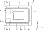
このような構成の圧電デバイスは、一般的に図10に示すような構成である。
すなわち、図10は圧電デバイス1の蓋体を省略した概略平面図である。
図において、圧電デバイス1は、パッケージ2内に圧電振動片4を収容して接合した構
成である。
The piezoelectric device having such a configuration is generally configured as shown in FIG.
That is, FIG. 10 is a schematic plan view in which the lid of the
In the figure, a
具体的には、パッケージ2は浅い箱状の収容体であり、パッケージ2の上側底面には、
接続用の電極部7,7が形成されている。この接続用電極部7,7は図示しないパッケー
ジ2の底面の実装端子と接続されている。
圧電振動片4は、例えば、矩形のATカット振動片で、その表裏の主面には、駆動用の
電極である励振電極5と、この励振電極5に接続された引出し電極6,6が形成されてい
る。この引出し電極6,6は裏面にも回り込んで形成されており、パッケージ2内の電極
部7,7の上に導電性接着剤8,8を塗布し、その上に圧電振動片4の引出し電極6,6
を載置して、導電性接着剤を硬化させることにより、接合されている。
Specifically, the
The piezoelectric vibrating
Are bonded by curing the conductive adhesive.
ところで、最近は、特にこのような圧電デバイス1について、小型化が極端に進展して
おり、圧電振動片4のX方向の寸法が1.5mm、Z方向の寸法が1.0mm、Y方向の
寸法(厚さt)が60μm程度のきわめて小型の圧電振動片も作られようとしている。
そして、圧電振動片だけでなく、圧電デバイス全体の小型化をはかるため、パッケージ
2も極端に小型化されている。
その結果、特に、パッケージ2のキャビティ2aの大きさに余裕がなくなり、上記した
圧電振動片4の接合作業においては、その角部4aなどがパッケージ2の内面などに干渉
し、きわめて作業がしにくかったり、圧電振動片4の一部端部がパッケージ2内面と干渉
したままきわめて不適切な傾斜姿勢で接合されてしまうという不都合がある。
また、最悪の場合、圧電振動片を接合する際に、パッケージ2のコーナ部に圧電振動片
が当たり、破損して結果的に圧電振動片の発振停止に至るおそれがある。
By the way, recently, especially such a
Further, not only the piezoelectric vibrating piece but also the entire piezoelectric device is downsized, the
As a result, the size of the
In the worst case, when the piezoelectric vibrating piece is joined, the piezoelectric vibrating piece may hit the corner portion of the
そこで、圧電振動片4の角部とパッケージ2の内側との干渉を防止するためには、該角
部を除去することが考えられる。
このような目的で、圧電振動片を加工することは、必ずしも知られていないが、他の目
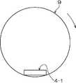
的で圧電振動片を形成するための製造工程において、面取りを行う技術については、図1
1に示すものが知られている(特許文献1参照)。
先ず圧電振動片を形成するための素片を形成する。この素片は、水晶ウエハを縦横に切
断し、その表面をラッピングして、短冊状のブランクした後、個々のブランクを重合状態
で接着剤などで固定し、ブランクの加工用ブロック4−1を形成する。
そして、図11の円筒パイプ9内に加工用ブロック4−1を入れ、矢印方向に円筒パイ
プ9を回転させると、加工用ブロック4−1を構成する各素片の稜線が研磨されて、面取
りされるものである。
In order to prevent interference between the corners of the piezoelectric vibrating
Although it is not always known to process a piezoelectric vibrating piece for such a purpose, FIG. 1 shows a technique for chamfering in a manufacturing process for forming a piezoelectric vibrating piece for other purposes.
1 is known (see Patent Document 1).
First, an element piece for forming a piezoelectric vibrating piece is formed. This piece is obtained by cutting a crystal wafer vertically and horizontally, lapping the surface, making a strip-shaped blank, fixing each blank in a polymerized state with an adhesive or the like, and attaching a blank processing block 4-1. Form.
Then, when the machining block 4-1 is placed in the
しかしながら、この特許文献1の技術により扱われる圧電振動片は、サイズが大きく、
そのため、円筒パイプ9などによる研磨技術が用いられるのであるが、上述したような圧
電振動片4は極めて小型で、それ自体、特許文献1のブランクのようにウエハのダイシン
グにより形成できる大きさではなく、例えば、水晶ウエハをエッチングすることにより外
形を抜いて、多数個同時に形成できるものである。
したがって、非常に小さいので、機械加工や研磨をすることは不可能である。
However, the piezoelectric vibrating piece handled by the technology of
Therefore, a polishing technique using a
Therefore, it is very small and cannot be machined or polished.
また、特許文献2には、圧電振動片について、その角部を機械加工や研磨ではなく、エ
ッチングにより加工することが記載されている。
本発明が対象とするような小型の圧電振動片においては、小型なために研磨などの加工
が不可能であれば、このようなエッチングにより加工する方法も考えられる。
In a small piezoelectric vibrating piece as the object of the present invention, if it is impossible to process such as polishing because it is small, a method of processing by such etching is also conceivable.
しかしながら、上記した特許文献2では、圧電振動片のX軸方向端面をエッチングによ
りC面取りすることが記載されている。
この文献では、小型の振動片に関しても、このようなエッチングを行うことで、従来の
コンベックス加工と同様にCI(クリスタルインピーダンス)値を改善することができる
というものである。
しかしながら、この手法は、圧電振動片のX軸方向端面をエッチングによりC面取りす
れば、できあがる形態から理解されるようにコンベックス加工と同様の効果が得られると
するもので、パッケージとの干渉箇所を面取りするものではない。
特に、特許文献2では、図1、図4に示す振動片1のコーナ部は、大きくR面取りされ
ているが、このような極端な量で大きくエッチングを行うと、エッチング異方性の影響が
強く出て、かえってCI値特性を損なうことが本発明者により確認されている。
However,
In this document, the CI (crystal impedance) value can be improved by performing such etching even for a small resonator element, as in the conventional convex processing.
However, in this method, if the end face in the X-axis direction of the piezoelectric vibrating piece is chamfered by etching, the same effect as the convex process can be obtained as understood from the completed form. It is not a chamfer.
In particular, in
本発明は、以上の課題を解決するためになされたもので、CI値特性を損なうことなく
、パッケージと干渉しにくい圧電振動片と、これを利用した圧電デバイスを提供すること
を目的とする。
SUMMARY An advantage of some aspects of the invention is to provide a piezoelectric vibrating piece that does not easily interfere with a package without impairing CI value characteristics, and a piezoelectric device using the same.
上述の目的は、第1の発明にあっては、圧電材料により矩形もしくは正方形の外形を備
えるように形成したきわめて小型の圧電振動片であって、前記外形の角部をエッチングに
より面取りした面取り部を設けるようにして、収容体であるパッケージとの干渉を避ける
構成とした圧電振動片により、達成される。
According to the first aspect of the present invention, the first invention is an extremely small piezoelectric vibrating piece formed of a piezoelectric material so as to have a rectangular or square outer shape, and a chamfered portion in which corner portions of the outer shape are chamfered by etching. This is achieved by the piezoelectric vibrating piece configured to avoid interference with the package as the container.
第1の発明の構成によれば、研磨などの機械加工がほとんど不可能であるきわめて小型
な圧電振動片について、その外形の角部をエッチングにより面取り加工している。これに
より、収容体であるパッケージなどのきわめて僅かなクリアランスしかない空間に、該圧
電振動片を収容する際に、該パッケージ内側と圧電振動片の角部が干渉することなく、精
密に接合される。
特に、所定の大きさの水晶ウエハなどの圧電基板をエッチングすることにより、多数個
の圧電振動片の素片を形成する工程を利用する場合には、当該エッチングによる外形加工
工程で使用するフォトマスクなどの前記角部に対応する箇所を、面取り形状に対応させれ
ば、外形加工と同時に面取り加工が行われるので、圧電振動片の外形加工後に、別の研磨
工程などで面取りしようとする従来の手法と比べても、利点が大きい。
さらに、圧電振動片の角部に限って、面取りを行うことで、X方向端面の全体をC面取
りするような従来の手法と比べて、極端なエッチング異方性の影響が出ることを有効に防
止でき、CI値特性の悪化を防ぐことができる。
According to the configuration of the first invention, the corners of the outer shape of a very small piezoelectric vibrating piece that cannot be machined such as polishing are chamfered by etching. As a result, when the piezoelectric vibrating reed is accommodated in a space having a very small clearance such as a package as a container, the inside of the package and the corner of the piezoelectric vibrating reed are precisely joined without interference. .
In particular, when using a process of forming a plurality of pieces of piezoelectric vibrating reeds by etching a piezoelectric substrate such as a quartz wafer of a predetermined size, a photomask used in the outer shape processing step by the etching If the part corresponding to the corner portion is made to correspond to the chamfered shape, chamfering is performed at the same time as the outer shape processing. Compared to the method, there are significant advantages.
Furthermore, by chamfering only the corners of the piezoelectric vibrating piece, it is effective that extreme etching anisotropy is exerted compared to the conventional method of chamfering the entire end face in the X direction. This can prevent the deterioration of the CI value characteristics.
第2の発明は、第1の発明の構成において、前記面取り部が、エッチング異方性により
CI値特性を悪化させない程度に面取りされていることを特徴とする。
第2の発明の構成によれば、圧電振動片の角部を面取りする上で、そのCI値特性を考
慮した加工を行うことで、接合の容易さを図ると同時に、性能の悪化を防止することがで
きる。
According to a second invention, in the configuration of the first invention, the chamfered portion is chamfered to such an extent that the CI value characteristic is not deteriorated by etching anisotropy.
According to the configuration of the second invention, when chamfering the corner portion of the piezoelectric vibrating piece, the processing considering the CI value characteristic is performed, thereby facilitating the joining and at the same time preventing the deterioration of the performance. be able to.
第3の発明は、第1または2のいずれかの発明の構成において、前記圧電振動片は、パ
ッケージ側に接合される基部と、該基部より先端側で、主として振動に関与する部分とを
有しており、前記先端側の端部における両角部のみに前記面取り部が形成されていること
を特徴とする。
第3の発明の構成によれば、パッケージ側に対して前記先端部を接合・固定しない場合
には、該先端部の角部に面取り部を設けることで、パッケージの内側などに該先端部が当
たり、水平な接合姿勢が乱れることなどを有効に防止することができる。
According to a third aspect of the invention, in the configuration of the first or second aspect of the invention, the piezoelectric vibrating piece has a base part joined to the package side and a part mainly involved in vibration on the tip side from the base part. The chamfered portion is formed only at both corners at the end on the tip side.
According to the configuration of the third invention, when the tip portion is not joined / fixed to the package side, the tip portion is provided inside the package or the like by providing a chamfered portion at a corner portion of the tip portion. It is possible to effectively prevent the horizontal joining posture from being disturbed.
第4の発明は、第1または2のいずれかの発明の構成において、前記圧電振動片の四隅
の角部に前記面取り部が形成されていることを特徴とする。
第4の発明の構成によれば、圧電振動片の全ての角部について、前記面取り部を設ける
ことにより、パッケージなどへの接合作業の際に、該パッケージ内側に当接する角部は一
切ないので、最も効果的である。
A fourth invention is characterized in that, in the configuration of either the first or second invention, the chamfered portions are formed at corners of four corners of the piezoelectric vibrating piece.
According to the configuration of the fourth aspect of the invention, by providing the chamfered portion for all the corner portions of the piezoelectric vibrating piece, there is no corner portion that contacts the inside of the package at the time of joining work to the package or the like. Is the most effective.
第5の発明は、第4の発明の構成において、前記四隅の角部のうち、パッケージ側に接
合される基部側の両角部に形成される面取り部が、先端の両角部に形成される面取り部よ
りも大きな面取り部であることを特徴とする。
第5の発明の構成によれば、圧電振動片が接合される領域は、ほとんど振動に関与しな
いので、この部分の面取り部を大きくしても性能に悪影響を与えることがほとんど無い反
面、大きな面取り部を有することはその分だけ、パッケージ内面への干渉を有効に防止す
ることができる。
According to a fifth aspect of the present invention, in the configuration of the fourth aspect, the chamfered portion formed at both corners on the base side joined to the package side among the corners of the four corners is formed at both corners of the tip. The chamfered portion is larger than the portion.
According to the configuration of the fifth aspect of the invention, the region to which the piezoelectric vibrating piece is joined hardly participates in vibration, so even if the chamfered portion of this portion is enlarged, the performance is hardly adversely affected. By having the portion, it is possible to effectively prevent interference with the inner surface of the package.
第6の発明は、第1または2のいずれかの発明の構成において、前記圧電振動片のパッ
ケージ側に接合される基部側の両角部にのみ前記面取り部が形成されていることを特徴と
する。
第6の発明の構成によれば、圧電振動片が接合される領域は、ほとんど振動に関与しな
いので、この部分にだけ面取り部を形成することにより、振動性能に悪影響を与えずに、
パッケージ内面への干渉を有効に防止する構造を得ることができる。
According to a sixth aspect of the present invention, in the configuration of the first or second aspect, the chamfered portion is formed only at both corners on the base side joined to the package side of the piezoelectric vibrating piece. .
According to the configuration of the sixth invention, the region to which the piezoelectric vibrating piece is joined hardly participates in the vibration. Therefore, by forming the chamfered portion only in this portion, the vibration performance is not adversely affected.
A structure that effectively prevents interference with the inner surface of the package can be obtained.
また、上述の目的は、第7の発明にあっては、パッケージまたはケース内にきわめて小
型の圧電振動片を収容した圧電デバイスであって、前記圧電振動片が、圧電材料により矩
形もしくは正方形の外形を備えるように形成され、かつ前記外形の角部をエッチングによ
り面取りした面取り部を設けるようにして、収容体であるパッケージとの干渉を避ける構
成とした圧電デバイスにより、達成される。
According to a seventh aspect of the present invention, there is provided a piezoelectric device in which a very small piezoelectric vibrating piece is accommodated in a package or a case, wherein the piezoelectric vibrating piece has a rectangular or square outer shape made of a piezoelectric material. And a chamfered portion in which a corner portion of the outer shape is chamfered by etching so as to avoid interference with a package as a container.
図1および図2は、本発明の圧電デバイスの第1の実施形態を示しており、図1は蓋体
を除いて内部構造を露出した圧電デバイスの概略平面図、図2は図1のA−A線概略端面
図であり、蓋体を配置して示すものである。
これらの図において、圧電デバイス30は、圧電振動子を構成した例を示しており、圧
電デバイス30は、パッケージ36内に圧電振動片を収容している。
具体的には、圧電デバイス30は、図2示すように、第1の基板34と、この第1の基
板34に積層された第2の基板35を含むパッケージ36内に圧電振動片31を収容して
いる。
1 and 2 show a first embodiment of a piezoelectric device according to the present invention. FIG. 1 is a schematic plan view of a piezoelectric device in which an internal structure is exposed except for a lid, and FIG. FIG. 6 is a schematic end view taken along the line A, and shows a lid disposed.
In these drawings, the
Specifically, as shown in FIG. 2, the
パッケージ36を構成する第1の基板34は絶縁基体であり、その上に電極部32が形
成されている。図1において、電極部は符号32,32に示されているように、パッケー
ジ36の端部において、第1の基板34の幅方向の両端部に一対設けられている。
第1の基板34と第2の基板35は絶縁材料で形成され、セラミックが適している。特
に、好ましい材料としては圧電振動片31や後述する蓋体の熱膨張係数と一致もしくは、
きわめて近い熱膨張係数を備えたものが選択され、この実施形態では、例えば、セラミッ
クのグリーンシートが利用されている。グリーンシートは、例えば、所定の溶液中にセラ
ミックパウダを分散させ、バインダを添加して生成される混練物をシート状の長いテープ
形状に成形し、これを所定の長さにカットして得られるものである。
The
The
A material having a very close thermal expansion coefficient is selected. In this embodiment, for example, a ceramic green sheet is used. The green sheet is obtained, for example, by dispersing a ceramic powder in a predetermined solution, forming a kneaded product formed by adding a binder into a sheet-like long tape shape, and cutting it into a predetermined length Is.
第1の基板34と第2の基板35は、図示する形状に成形したグリーンシートを積層し
、焼結して形成することができる。この場合、第1の基板34は、パッケージ36の底部
を構成する基板で、これに重ねられる第2の基板35は、上述したグリーンシートを板状
として、内部の材料を除去して、枠状として、図2の内部空間Sを形成したもので、この
内部空間S(図3参照)を利用して、圧電振動片31を収容するようにしている。このパ
ッケージ36には、セラミックやガラスあるいはコバールなどの金属で形成された蓋体3
7がコバールリングなどの接合材もしくは封止材47などを介して接合されている。これ
により、パッケージ36は気密に封止されている。
The
7 is joined via a joining material such as a Kovar ring or a sealing
第1の基板34上には、例えば、銀・パラジウムなどの導電ペーストもしくはタングス
テンメタライズなどの導電ペーストなどを用いて、必要とされる導電パターンを形成後に
、第1及び第2の基板の焼結をした後で、ニッケルおよび金もしくは銀などを順次メッキ
して、上述した電極部32,32が形成されている。図2に示すように、電極部32は、
パッケージ36の底面に露出した実装端子41,41と図示しない導電パターンにより接
続されている。この電極部32と実装端子41とを接続するための導電パターンは、パッ
ケージ36の形成時に利用されるキャスタレーション(図示せず)の表面に形成して、パ
ッケージ36の外面を引き回してもよいし、あるいは第1の基板34を貫通する図示しな
い導電スルーホールなどにより接続してもよい。
On the
The mounting
圧電振動片31は、後述するように、例えば圧電材料により形成されたウエハを厚みの
薄い矩形もしくは正方形に加工したものである。この圧電振動片31は、きわめて小型で
、例えば、図1において、X(電機軸)方向の寸法が1.5mm、Z(光軸)方向の寸法
が1.0mm、Y(機械軸)方向の寸法(厚さt)が60μm程度である。
この圧電振動片31を形成する圧電材料は、具体的には、圧電基板として、水晶から作
る水晶ウエハが用いられ、この水晶ウエハは、該水晶のX軸(電機軸)に対して平行で、
しかもZ軸(光軸)に対してカット面をもつ水晶基板が使用される。
この場合、水晶ウエハは水晶の結晶軸に関して、X軸が電気軸、Y軸が機械軸及びZ軸
が光軸となるように、水晶の単結晶から切り出されることになる。また、水晶の単結晶か
ら切り出す際、上述のX軸、Y軸及びZ軸からなる直交座標系において、Z軸から所定角
度、例えば、35.15度傾けた面で切り出したATカット水晶板を得るようにしたもの
で、それに後述する駆動電極を形成している。なお、これ以外の圧電材料として、例えば
、水晶以外にもタンタル酸リチウム,ニオブ酸リチウム等の圧電材料を利用することがで
きる。また、圧電チップの形状もフラットタイプに限らず、コンベックスタイプや、逆メ
サ型の振動片を用いることができる。
As will be described later, the piezoelectric vibrating
Specifically, the piezoelectric material forming the piezoelectric vibrating
Moreover, a quartz substrate having a cut surface with respect to the Z axis (optical axis) is used.
In this case, the crystal wafer is cut out from the single crystal of the crystal so that the X axis is the electric axis, the Y axis is the mechanical axis, and the Z axis is the optical axis. In addition, when cutting from a single crystal of quartz, an AT-cut quartz plate cut out at a predetermined angle, for example, 35.15 degrees from the Z axis in the above-described orthogonal coordinate system consisting of the X, Y, and Z axes. The drive electrode which will be described later is formed. As other piezoelectric materials, for example, piezoelectric materials such as lithium tantalate and lithium niobate can be used in addition to quartz. Further, the shape of the piezoelectric chip is not limited to the flat type, and a convex type or a reverse mesa type resonator element can be used.
図1において、振動片の個片である圧電チップの表面には、駆動用の主電極として、励
振電極51が形成されている。励振電極51は、圧電チップの積極的に振動させようとす
る領域に形成され、圧電材料に駆動電圧を印加することで、材料内に効率よく電界を生じ
させ、励振するためのものである。励振電極51は、図示しない圧電チップの裏面にも同
様の形態で形成され、それぞれ圧電振動片31の長さ方向の端部において、その幅方向の
両端にそれぞれ形成された接続電極である引出し電極51a,51aに対して、各別に接
続されている。各引出し電極51a,51aは圧電チップの側面を回り込んで、裏面にも
形成されている。
In FIG. 1, an
このような圧電振動片31は、図1に示されているように、パッケージ36側の各電極
部32,32の上に導電性接着剤43,43を塗布し、その上に圧電振動片31の図1で
説明した各引出し電極51a,51aが形成されている基部もしくは一端部31aを載置
して、これら導電性接着剤43,43を硬化させることにより片持ち式に接合されている
。
これにより、パッケージ36の外部から実装端子41,41を介して供給された駆動電
圧は、パッケージ36側の電極部32,32から導電性接着剤43,43および圧電振動
片31の引出し電極51a,51aを介して、励振電極51に印加される。したがって、
圧電振動片31の先端側31bは圧電作用により振動することで、駆動されるようになっ
ている。
As shown in FIG. 1, such a piezoelectric vibrating
As a result, the drive voltage supplied from the outside of the
The
ここで、導電性接着剤43,43としては、所定の合成樹脂でなるバインダー成分に、
銀粒子などの導電粒子を添加したものを使用することができる。また、圧電振動片31は
必ずしも片持ち式でなく、先端側31bの一部をパッケージ36側に設けた図示しない「
枕」と称する台に載置した構成としてもよい。
Here, as the
What added electroconductive particles, such as silver particle, can be used. Further, the piezoelectric vibrating
It is good also as a structure mounted on the stand called a pillow.
さらに、図1に示すように、圧電振動片31の先端側の角部を後述するようにエッチン
グにより面取りした面取り部48,48を設けている。すなわち、この実施形態では、研
磨などの機械加工がほとんど不可能であるきわめて小型な圧電振動片について、その外形
の角部をエッチングにより面取り加工している。
このため、収容体であるパッケージ36のきわめて僅かなクリアランスしかない空間S
に、圧電振動片31を収容する際に、パッケージ36の凹状のコーナ部36a,36aと
圧電振動片31の角部が干渉することなく、精密に接合される。
さらに、圧電振動片31の角部に限って、面取りを行うことで、X方向端面の全体をC
面取りするような従来の手法と比べて、極端なエッチング異方性の影響が出ることを有効
に防止でき、CI値特性の悪化を防ぐことができる。
Further, as shown in FIG. 1, chamfered
For this reason, the space S having a very small clearance of the
In addition, when the piezoelectric vibrating
Further, by chamfering only the corners of the piezoelectric vibrating
Compared with the conventional method of chamfering, it is possible to effectively prevent the influence of extreme etching anisotropy and to prevent the deterioration of the CI value characteristics.
次に、このような小型の圧電振動片31を作る方法について、簡単に説明する。
図3は、圧電振動片31の製造方法の一例を示すフローチャート、図4および図5は圧
電振動片31の製造工程の一例を順次に示す工程図、図6は水晶ウエハから多数の圧電振
動片を製造する様子を示す図である。
図3(a)の水晶ウエハ56は、上述したように、水晶の結晶軸に関して、X軸が電気
軸、Y軸が機械軸及びZ軸が光軸となるように、水晶の単結晶から切り出されたものであ
る。
この水晶ウエハ56を先ず純水で洗浄し(ST11)、図4(b)に示すように、水晶
ウエハ56の表面にスパッタリングや真空蒸着などにより、下地層のクロム層52を成膜
し、その表面にさらに金層53を成膜する(ST12)。
Next, a method for producing such a small piezoelectric vibrating
FIG. 3 is a flowchart showing an example of a method for manufacturing the piezoelectric vibrating
As described above, the
The
続いて、金層の表面にレジスト54を塗布する(ST13)。レジスト54としては、
例えば、東京応化工業株式会社製のOFPR−800が使用される。
このレジスト54は、露光・現像され(ST14,ST15)、図5(c)に示すよう
に、開口54aが形成される。この開口54aの一部には、図1の面取り部48に対応し
た面取り形成用開口54bが形成される。
次に、例えば、よう素及びよう化アルカリ溶液を用いて、金層53をウエットエッチン
グし、次いで、硝酸2セリウムアンモニウム溶液により、クロム層52をエッチングする
(ST16)。
Subsequently, a resist 54 is applied to the surface of the gold layer (ST13). As the resist 54,
For example, OFPR-800 manufactured by Tokyo Ohka Kogyo Co., Ltd. is used.
The resist 54 is exposed and developed (ST14, ST15), and an
Next, the
このようにして、図5(d)に示すように露出した水晶部分を、フッ酸溶液などを用い
て、ウエットエッチングする(ST17)。これにより、図5(e)に示す状態となり、
外形55が分離される。続いて、レジスト54を剥離し、金層53とクロム層52とを順
次剥離する(ST18,ST19)。これにより図6に示すように、1枚の水晶ウエハ5
6について多数個の振動片の個片である圧電チップ31−1が同時に形成されるので、S
T19の剥離工程で適切なフォトリソグラフィの工程を実行することで、励振電極と引出
し電極などの電極を形成でき、圧電振動片31を形成することができる。
かくして、圧電振動片31をエッチングにより多数個同時形成する際に、面取り部48
も同時に形成できるものである。
In this way, the exposed quartz portion as shown in FIG. 5D is wet-etched using a hydrofluoric acid solution or the like (ST17). As a result, the state shown in FIG.
The
6, the piezoelectric chip 31-1, which is an individual piece of a large number of vibrating pieces, is formed at the same time.
By performing an appropriate photolithography process in the peeling process of T19, electrodes such as an excitation electrode and an extraction electrode can be formed, and the piezoelectric vibrating
Thus, when a large number of piezoelectric vibrating
Can also be formed at the same time.
図7は、圧電デバイスの第2の実施形態を示す概略平面図であり、図1と同じ符号を付
した箇所は共通する構成であるから、重複する説明は省略し、以下、相違点を中心に説明
する。
図7の圧電デバイス30−1では、圧電振動片31の四隅の角部に面取り部48,48
,49,49が形成されている。すなわち、図1の場合と比較すると、パッケージ36の
凹状のコーナ部36b,36bに対応する箇所にも面取り部49,49を追加している。
これにより、圧電振動片31の全ての角部について、パッケージ36の内側と干渉しない
ので、接合作業の際に、該パッケージ内側に当接する角部は一切ないものである。
FIG. 7 is a schematic plan view showing a second embodiment of the piezoelectric device, and the portions denoted by the same reference numerals as those in FIG. Explained.
In the piezoelectric device 30-1 in FIG. 7, chamfered
, 49, 49 are formed. That is, as compared with the case of FIG. 1, chamfered
Thereby, since all the corners of the piezoelectric vibrating
図8は、圧電振動片が上述した寸法とされた場合に、面取り量(図1の符号Kの寸法で
示す)と、CI値の関係を示す図である。
エッチングにより面取りを行う場合において、従来のように角部を大きく面取りし、X
方向端面をC面取りすると、その分、水晶のエッチング異方性の影響が大きくなり、バリ
として異形部が形成される。エッチング量が多いと、すなわちR(曲面)形状が大きいと
、その曲面の各位置で結晶方位のエッチング面が連続して表れるから、バリが大きくなり
、図示のようにCI値が大きくなる。
また、図示されているように、面取り量は300μm以下とした時、CI値の上昇が比
較的少なく、100<K<300(μm)の場合がよりCI値の上昇を抑えることができ
るものであり、さらに、Kは100μmより小さい場合が、最もCI値の上昇が少ない。
このように、面取り部を形成する場合には、できるだけR形状としないで、直線的に切
り落とした形態であることが好ましく、さらに圧電振動片を有限要素法で解析する上でも
矩形の圧電振動片として、直線的に切り落とした面取り部とすることで、解析が容易にな
る。
FIG. 8 is a diagram illustrating the relationship between the chamfering amount (indicated by the dimension indicated by the symbol K in FIG. 1) and the CI value when the piezoelectric vibrating piece has the above-described dimensions.
When chamfering is performed by etching, the corners are chamfered as in the past, and X
If the direction end face is chamfered, the influence of the etching anisotropy of the crystal is increased correspondingly, and a deformed portion is formed as a burr. When the etching amount is large, that is, when the R (curved surface) shape is large, an etched surface having a crystal orientation appears continuously at each position on the curved surface, so that burrs increase and the CI value increases as shown in the figure.
Also, as shown in the figure, when the chamfering amount is 300 μm or less, the increase in the CI value is relatively small, and the increase in the CI value can be further suppressed when 100 <K <300 (μm). In addition, when the K is smaller than 100 μm, the increase in the CI value is the smallest.
As described above, when forming the chamfered portion, it is preferable that the chamfered portion is not cut into an R shape as much as possible, but is cut in a straight line. As a chamfered portion cut off linearly, the analysis becomes easy.
図9は、圧電デバイスの第3の実施形態を示す概略平面図であり、図1と同じ符号を付
した箇所は共通する構成であるから、重複する説明は省略し、以下、相違点を中心に説明
する。
図9の圧電デバイス30−2では、圧電振動片31の四隅の角部に面取り部が形成され
ているだけでなく、四隅の角部のうち、パッケージ36側に接合される基部31a側の両
角部に形成される面取り部49−1,49−1が、先端側31bの両角部に形成される面
取り部48,48よりも大きな面取り部とされている。
すなわち、圧電振動片31の基部31aは接合されるため、ほとんど振動に関与しない
ので、この部分の面取り部49−1,49−1を大きくしても性能に悪影響を与えること
がほとんど無い反面、大きな面取り部を有することはその分だけ、パッケージ36内面へ
の干渉を有効に防止することができる。
FIG. 9 is a schematic plan view showing a third embodiment of the piezoelectric device, and portions having the same reference numerals as those in FIG. Explained.
In the piezoelectric device 30-2 of FIG. 9, not only chamfered portions are formed at the corners of the four corners of the piezoelectric vibrating
That is, since the
また、特に本実施形態の面取り部49−1は段部を有するように交差面を有する形態い
るため、当該面取り部の面積が大きくなっており、導電性接着剤43との接合強度を向上
させることができる。
In particular, since the chamfered portion 49-1 of the present embodiment has an intersecting surface so as to have a stepped portion, the area of the chamfered portion is increased and the bonding strength with the
また、図示しないが、上述の原理と同様の理由により、圧電振動片31の基部31a側
の両角部にだけ面取り部を設ければ、全ての角部に面取り部を形成した第2の実施形態と
比較すると、パッケージ36への干渉の点では劣るものの、CI値の上昇など振動特性へ
の悪影響な殆どないので、好ましい。
Although not shown in the drawings, for the same reason as described above, if chamfered portions are provided only at both corners on the
本発明は上述の実施形態に限定されない。各実施形態の各構成はこれらを適宜組み合わ
せたり、省略し、図示しない他の構成と組み合わせることができる。
本発明は、ATカット圧電振動片だけでなく、所謂コンベックスタイプの圧電振動片や
、逆メサ形状の圧電振動片などにも利用することができる。
また、この発明は、箱状の収容容器としてのパッケージを利用し、内部に圧電振動片を
収容するものであれば、圧電振動子、圧電発振器等の名称にかかわらず、全ての圧電デバ
イスに適用することができる。
The present invention is not limited to the above-described embodiment. Each configuration of each embodiment can be appropriately combined or omitted, and can be combined with other configurations not shown.
The present invention can be used not only for an AT-cut piezoelectric vibrating piece, but also for a so-called convex type piezoelectric vibrating piece, an inverted mesa-shaped piezoelectric vibrating piece, and the like.
In addition, the present invention is applicable to all piezoelectric devices regardless of the names of piezoelectric vibrators, piezoelectric oscillators, etc., as long as they use a package as a box-shaped container and accommodate a piezoelectric vibrating piece inside. can do.
30・・・圧電デバイス、31・・・圧電振動片、36・・・パッケージ、48、49
・・・面取り部、51・・・励振電極
30 ... piezoelectric device, 31 ... piezoelectric vibrating piece, 36 ... package, 48, 49
... Chamfered part, 51 ... Excitation electrode
Claims (7)
振動片であって、
前記外形の角部をエッチングにより面取りした面取り部を設けるようにして、収容体で
あるパッケージとの干渉を避ける構成とした
ことを特徴とする圧電振動片。 An extremely small piezoelectric vibrating piece formed of a piezoelectric material so as to have a rectangular or square outer shape,
A piezoelectric vibrating piece, characterized in that a chamfered portion in which a corner portion of the outer shape is chamfered by etching is provided to avoid interference with a package as a container.
ていることを特徴とする請求項1に記載の圧電振動片。 2. The piezoelectric vibrating piece according to claim 1, wherein the chamfered portion is chamfered to such an extent that the CI value characteristic is not deteriorated by etching anisotropy.
振動に関与する部分とを有しており、前記先端側の端部における両角部のみに前記面取り
部が形成されていることを特徴とする請求項1または2のいずれかに記載の圧電振動片。 The piezoelectric vibrating piece has a base part joined to the package side and a part mainly involved in vibration on the tip side from the base part, and the chamfered part is only at both corners at the end part on the tip side. The piezoelectric vibrating piece according to claim 1, wherein the piezoelectric vibrating piece is formed.
1または2のいずれかに記載の圧電振動片。 The piezoelectric vibrating piece according to claim 1, wherein the chamfered portion is formed at corners of four corners of the piezoelectric vibrating piece.
部が、先端の両角部に形成される面取り部よりも大きな面取り部であることを特徴とする
請求項4に記載の圧電振動片。 The chamfered portion formed at both corners on the base side joined to the package side among the corners of the four corners is a chamfered portion larger than the chamfered portion formed at both corners of the tip. Item 5. The piezoelectric vibrating piece according to Item 4.
されていることを特徴とする請求項1または2のいずれかに記載の圧電振動片。 3. The piezoelectric vibrating piece according to claim 1, wherein the chamfered portion is formed only at both corners on the base side bonded to the package side of the piezoelectric vibrating piece. 4.
て、
前記圧電振動片が、
圧電材料により矩形もしくは正方形の外形を備えるように形成され、
かつ前記外形の角部をエッチングにより面取りした面取り部を設けるようにして、収容
体であるパッケージとの干渉を避ける構成とした
ことを特徴とする圧電デバイス。 A piezoelectric device containing a very small piezoelectric vibrating piece in a package or case,
The piezoelectric vibrating piece is
It is formed to have a rectangular or square outer shape with piezoelectric material,
In addition, the piezoelectric device is characterized in that a chamfered portion in which a corner portion of the outer shape is chamfered by etching is provided so as to avoid interference with a package as a container.
Priority Applications (1)
| Application Number | Priority Date | Filing Date | Title |
|---|---|---|---|
| JP2005348791A JP2007158566A (en) | 2005-12-02 | 2005-12-02 | Piezoelectric vibration chip and piezoelectric device |
Applications Claiming Priority (1)
| Application Number | Priority Date | Filing Date | Title |
|---|---|---|---|
| JP2005348791A JP2007158566A (en) | 2005-12-02 | 2005-12-02 | Piezoelectric vibration chip and piezoelectric device |
Publications (2)
| Publication Number | Publication Date |
|---|---|
| JP2007158566A true JP2007158566A (en) | 2007-06-21 |
| JP2007158566A5 JP2007158566A5 (en) | 2008-12-11 |
Family
ID=38242375
Family Applications (1)
| Application Number | Title | Priority Date | Filing Date |
|---|---|---|---|
| JP2005348791A Pending JP2007158566A (en) | 2005-12-02 | 2005-12-02 | Piezoelectric vibration chip and piezoelectric device |
Country Status (1)
| Country | Link |
|---|---|
| JP (1) | JP2007158566A (en) |
Cited By (7)
| Publication number | Priority date | Publication date | Assignee | Title |
|---|---|---|---|---|
| JP2009194631A (en) * | 2008-02-14 | 2009-08-27 | Seiko Instruments Inc | Wafer, wafer polishing device, method of polishing wafer, method of manufacturing piezoelectric vibrator, piezoelectric vibrator, oscillator, electronic equipment, and radio clock |
| CN103944531A (en) * | 2013-01-18 | 2014-07-23 | 精工爱普生株式会社 | Resonator element, resonator, oscillator, electronic apparatus and moving object |
| JP2014209719A (en) * | 2013-03-29 | 2014-11-06 | セイコーエプソン株式会社 | Vibration element, vibrator, oscillator, electronic apparatus, and mobile body |
| JP2017108379A (en) * | 2015-11-27 | 2017-06-15 | 株式会社大真空 | Piezoelectric vibrator |
| JP2019009619A (en) * | 2017-06-23 | 2019-01-17 | セイコーエプソン株式会社 | Vibration element, vibrator, generator, electronic apparatus, and mobile body |
| JP7365182B2 (en) | 2019-10-04 | 2023-10-19 | 日本電波工業株式会社 | Oscillator and oscillator |
| JP7396858B2 (en) | 2019-11-01 | 2023-12-12 | 日本電波工業株式会社 | Piezoelectric device and its manufacturing method |
Citations (5)
| Publication number | Priority date | Publication date | Assignee | Title |
|---|---|---|---|---|
| JPS6363209A (en) * | 1986-09-04 | 1988-03-19 | Matsushima Kogyo Co Ltd | Manufacture of piezoelectric vibrator |
| JP2000013169A (en) * | 1998-06-18 | 2000-01-14 | Toyo Commun Equip Co Ltd | Piezoelectric oscillator |
| JP2003318697A (en) * | 2002-04-25 | 2003-11-07 | Seiko Instruments Inc | At-cut quartz resonator |
| JP2005012635A (en) * | 2003-06-20 | 2005-01-13 | Toyo Commun Equip Co Ltd | Piezoelectric device |
| JP2005217727A (en) * | 2004-01-29 | 2005-08-11 | Daishinku Corp | Piezoelectric vibration device |
-
2005
- 2005-12-02 JP JP2005348791A patent/JP2007158566A/en active Pending
Patent Citations (5)
| Publication number | Priority date | Publication date | Assignee | Title |
|---|---|---|---|---|
| JPS6363209A (en) * | 1986-09-04 | 1988-03-19 | Matsushima Kogyo Co Ltd | Manufacture of piezoelectric vibrator |
| JP2000013169A (en) * | 1998-06-18 | 2000-01-14 | Toyo Commun Equip Co Ltd | Piezoelectric oscillator |
| JP2003318697A (en) * | 2002-04-25 | 2003-11-07 | Seiko Instruments Inc | At-cut quartz resonator |
| JP2005012635A (en) * | 2003-06-20 | 2005-01-13 | Toyo Commun Equip Co Ltd | Piezoelectric device |
| JP2005217727A (en) * | 2004-01-29 | 2005-08-11 | Daishinku Corp | Piezoelectric vibration device |
Cited By (10)
| Publication number | Priority date | Publication date | Assignee | Title |
|---|---|---|---|---|
| JP2009194631A (en) * | 2008-02-14 | 2009-08-27 | Seiko Instruments Inc | Wafer, wafer polishing device, method of polishing wafer, method of manufacturing piezoelectric vibrator, piezoelectric vibrator, oscillator, electronic equipment, and radio clock |
| CN103944531A (en) * | 2013-01-18 | 2014-07-23 | 精工爱普生株式会社 | Resonator element, resonator, oscillator, electronic apparatus and moving object |
| JP2014138413A (en) * | 2013-01-18 | 2014-07-28 | Seiko Epson Corp | Vibration element, vibrator, oscillator, electronic device, and mobile unit |
| CN103944531B (en) * | 2013-01-18 | 2018-03-16 | 精工爱普生株式会社 | Vibrating elements, oscillator, oscillator, electronic equipment and moving body |
| JP2014209719A (en) * | 2013-03-29 | 2014-11-06 | セイコーエプソン株式会社 | Vibration element, vibrator, oscillator, electronic apparatus, and mobile body |
| JP2017108379A (en) * | 2015-11-27 | 2017-06-15 | 株式会社大真空 | Piezoelectric vibrator |
| JP2019009619A (en) * | 2017-06-23 | 2019-01-17 | セイコーエプソン株式会社 | Vibration element, vibrator, generator, electronic apparatus, and mobile body |
| US11177429B2 (en) | 2017-06-23 | 2021-11-16 | Seiko Epson Corporation | Vibrator element, vibrator, oscillator, electronic apparatus, and vehicle |
| JP7365182B2 (en) | 2019-10-04 | 2023-10-19 | 日本電波工業株式会社 | Oscillator and oscillator |
| JP7396858B2 (en) | 2019-11-01 | 2023-12-12 | 日本電波工業株式会社 | Piezoelectric device and its manufacturing method |
Similar Documents
| Publication | Publication Date | Title |
|---|---|---|
| JP5589167B2 (en) | Piezoelectric vibrating piece and piezoelectric vibrator | |
| JP4715652B2 (en) | Piezoelectric vibrating piece | |
| EP2624450B1 (en) | Piezoelectric vibrating reed, piezoelectric vibrator, method for manufacturing piezoelectric vibrating reed, and method for manufacturing piezoelectric vibrator | |
| JP2007158566A (en) | Piezoelectric vibration chip and piezoelectric device | |
| US20150015119A1 (en) | Piezoelectric vibrating piece, method for fabricating piezoelectric vibrating piece, piezoelectric device, and method for fabricating piezoelectric device | |
| TW201351737A (en) | Piezoelectric vibrating piece and piezoelectric device | |
| JP4292825B2 (en) | Method for manufacturing quartz vibrating piece | |
| JP5708079B2 (en) | Crystal oscillator | |
| US11824521B2 (en) | Vibration substrate having a pair of holding portions and a beam portion connecting the holding portions, vibrator, and vibrator unit | |
| JP5049479B2 (en) | Quartz device and manufacturing method thereof | |
| JP4935490B2 (en) | Piezoelectric device | |
| JP4591035B2 (en) | Piezoelectric vibrating piece and method for manufacturing piezoelectric device | |
| JP2002261574A (en) | Crystal oscillator and its producing method | |
| JP2007173906A (en) | Method of manufacturing piezoelectric resonator chip and piezoelectric device | |
| JP2006086726A (en) | Piezoelectric vibration chip, piezoelectric device and method of manufacturing the same | |
| JP2014176071A (en) | Piezoelectric vibration piece and piezoelectric device | |
| JP5018852B2 (en) | Method for manufacturing piezoelectric device | |
| JP2007049541A (en) | Piezoelectric device | |
| JP4938366B2 (en) | Piezoelectric vibrator | |
| JP2008283597A (en) | Manufacturing methods of component storage container and piezoelectric device | |
| JP2005210185A (en) | Manufacturing method of piezoelectric vibrating piece and piezoelectric device | |
| JP5141737B2 (en) | Quartz crystal resonator element, crystal device manufacturing method, and crystal device | |
| JP4541983B2 (en) | Piezoelectric vibrator | |
| JP2008118241A (en) | Electronic device and manufacturing method thereof | |
| JP2017112544A (en) | Piezoelectric vibrator |
Legal Events
| Date | Code | Title | Description |
|---|---|---|---|
| RD04 | Notification of resignation of power of attorney |
Free format text: JAPANESE INTERMEDIATE CODE: A7424 Effective date: 20070404 |
|
| A521 | Request for written amendment filed |
Free format text: JAPANESE INTERMEDIATE CODE: A523 Effective date: 20081028 |
|
| A621 | Written request for application examination |
Free format text: JAPANESE INTERMEDIATE CODE: A621 Effective date: 20081028 |
|
| A131 | Notification of reasons for refusal |
Free format text: JAPANESE INTERMEDIATE CODE: A131 Effective date: 20100309 |
|
| A521 | Request for written amendment filed |
Free format text: JAPANESE INTERMEDIATE CODE: A523 Effective date: 20100507 |
|
| A02 | Decision of refusal |
Free format text: JAPANESE INTERMEDIATE CODE: A02 Effective date: 20100622 |