JP4591035B2 - Piezoelectric vibrating piece and method for manufacturing piezoelectric device - Google Patents
Piezoelectric vibrating piece and method for manufacturing piezoelectric device Download PDFInfo
- Publication number
- JP4591035B2 JP4591035B2 JP2004306887A JP2004306887A JP4591035B2 JP 4591035 B2 JP4591035 B2 JP 4591035B2 JP 2004306887 A JP2004306887 A JP 2004306887A JP 2004306887 A JP2004306887 A JP 2004306887A JP 4591035 B2 JP4591035 B2 JP 4591035B2
- Authority
- JP
- Japan
- Prior art keywords
- vibrating piece
- piezoelectric
- piezoelectric vibrating
- manufacturing
- base
- Prior art date
- Legal status (The legal status is an assumption and is not a legal conclusion. Google has not performed a legal analysis and makes no representation as to the accuracy of the status listed.)
- Expired - Fee Related
Links
Images


Description
本発明は、パッケージまたはケースに収容するための圧電振動片と、この圧電振動片をパッケージやケースに収容した圧電デバイスとをそれぞれ製造する方法に関する。 The present invention relates to a method of manufacturing a piezoelectric vibrating piece for housing in a package or case and a piezoelectric device having the piezoelectric vibrating piece housed in a package or case.
HDD(ハード・ディスク・ドライブ)、モバイルコンピュータ、あるいはICカード等の小型の情報機器や、携帯電話、自動車電話、またはページングシステム等の移動体通信機器やジャイロセンサなどの計測機器において、パッケージなどの内部に圧電振動片を収容した圧電振動子や圧電発振器等の圧電デバイスが広く使用されている。
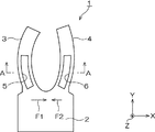
図8は、このような圧電デバイスに使用される圧電振動片の公知の構成例(特許文献1参照)を簡略化して示す概略平面図である。
Packages such as small information devices such as HDDs (hard disk drives), mobile computers, IC cards, mobile communication devices such as mobile phones, car phones, and paging systems, and measuring devices such as gyro sensors Piezoelectric devices such as piezoelectric vibrators and piezoelectric oscillators that house a piezoelectric vibrating piece inside are widely used.
FIG. 8 is a schematic plan view schematically showing a known configuration example (see Patent Document 1) of a piezoelectric vibrating piece used in such a piezoelectric device.
図において、圧電振動片1は、例えば水晶の単結晶から形成されており、幅広の基部2と、この基部から同じ方向に平行に延びる2本の振動腕3,4とを備えている。図9は図8のA−A線切断端面図であり、振動腕3,4には、それぞれ、表裏面に長さ方向に延びる長溝5,6が形成されている。この長溝5,6には、図示しない駆動電極としての励振電極が形成されている。
これにより、外部から励振電極に駆動電圧が印加されることで、振動腕3,4内に効率よく電界が発生し、各振動腕3,4は、図8に示すように、その先端部を互いに接近・離間されるように屈曲振動するようになっている。そして、このような振動に基づく振動周波数を取り出すことにより、制御用のクロック信号等の基準信号に利用されるようになっている。
In the figure, the piezoelectric
As a result, an electric field is efficiently generated in the vibrating
この圧電振動片1の各振動腕3,4と、これら振動腕3,4の長溝5,6は、ウエハ状にした圧電材料でなる基板をエッチングすることにより形成されている。すなわち、一般的には、まず、ウエハ基板をエッチングして、図8のような音叉状の外形を形成し、その後図9で説明した長溝5,6をハーフエッチングすることにより形成される。
ところが、このような圧電振動片1においては、その外形エッチング工程でのウエットエッチングでは、図8、図9に示した電気軸X、機械軸Y、光学軸Zに関して、エッチングの進行スピードに相違が見られ、このようなエッチング異方性により、長溝5,6内には、平らな底面を形成することができない。
この結果、例えば、振動腕3について見ると、長溝5を挟んだ両側壁部5a,5bの厚みが左右で相違し、この結果、振動腕3は図9に示す仮想の中心線CEに関して、左右の側壁部の剛性が相違する。すなわち、左側の壁部5aが剛性が高く、右側の壁部5bの剛性はこれより低くなる。
However, in such a piezoelectric vibrating
As a result, for example, when viewing the vibrating
このため、図8のように各振動腕3,4が屈曲振動している状態では、それぞれ、水平方向に左右に屈曲する際の変形度が異なるため、左右の振動腕3,4の屈曲バランスが崩れてしまう。これにより、各振動腕3,4の変形によって基部2に伝えられる応力もF1,F2が均衡することがないので、打ち消すことができず、Z方向変位や、Y方向変位の原因となり、CI(クリスタルインピーダンス)値の増大を招くと考えられる。
ここで、圧電振動片をエッチングにより形成する際に、長時間かけてウエットエッチングすることで、図9において長溝5,6を挟んでいる両側の壁部5a,5bのうち、左側の壁部5aの厚みを十分薄くして、左右の剛性をバランスさせることができる。
しかしながら、その場合には、従来よりも非常に長い時間をエッチング工程に費やさなければならず、生産性が低くなってしまう。
加えて、圧電振動片1が小型化されると、その分長溝5の幅W1が狭くなる。この幅W1が非常に狭くなった場合には、エッチャントが回り込みにくくなり、長時間かけてウエットエッチングした場合でも左右の壁部5a,5bの厚みを等しくできない。
For this reason, in the state in which the vibrating
Here, when the piezoelectric vibrating piece is formed by etching, wet etching is performed for a long time, so that the
However, in that case, a much longer time than in the past must be spent in the etching process, resulting in lower productivity.
In addition, when the piezoelectric vibrating
また、圧電振動片を形成する場合のエッチング異方性がないドライエッチングにより圧電振動片1の外形および長溝を加工形成することが考えられる。
しかしながら、ドライエッチングは、ウエットエッチングに比べるとはるかに長い時間を必要とし、この場合にも生産性が著しく悪化するという問題がある。
Further, it is conceivable to process and form the outer shape and the long groove of the piezoelectric vibrating
However, dry etching requires much longer time than wet etching, and also in this case, there is a problem that productivity is remarkably deteriorated.
この発明は、振動バランスを改善し、CI値を低く抑えることができるようにした圧電振動片と圧電デバイスとを、短時間で製造するための製造方法を提供することを目的とする。 It is an object of the present invention to provide a manufacturing method for manufacturing a piezoelectric vibrating piece and a piezoelectric device that can improve the vibration balance and keep the CI value low.
上記の目的は、第1の発明にあっては、基部と、この基部と一体に形成され、かつ前記基部から平行に延びる少なくとも一対の振動腕と、前記各振動腕の長さ方向に形成される長溝とを備える圧電振動片の外形と前記長溝とをエッチングにより形成する圧電振動片の製造方法であって、前記圧電基板を用意し、前記圧電振動片の外形を形成後、
前記長溝の位置に、前記長溝よりも浅い溝をウエットエッチングによって形成した後、
浅く形成した前記溝の底部をドライエッチングにより加工する圧電振動片の製造方法により、達成される。
In the first invention, the above object is formed in the length direction of the base, at least a pair of vibrating arms formed integrally with the base, and extending in parallel from the base. A piezoelectric vibrating reed manufacturing method for forming an outer shape of a piezoelectric vibrating piece having a long groove and the long groove by etching, the piezoelectric substrate is prepared, and after forming the outer shape of the piezoelectric vibrating piece,
After forming a groove shallower than the long groove by wet etching at the position of the long groove,
This is achieved by a method for manufacturing a piezoelectric vibrating piece in which a shallow bottom portion of the groove is processed by dry etching .
第1の発明の構成によれば、圧電振動片の外形加工だけでなく、長溝の加工も途中まで従来と同じウエットエッチングで行い、ある程度長溝が形成された時点で、ドライエッチングに切り換えることになるので、従来の製造に要していた時間が、極端に延長されることなく、振動バランスを改善し、CI値を低く抑えることができるようにした圧電振動片を迅速に加工形成することができる。
According to the configuration of the first invention , not only the outer shape processing of the piezoelectric vibrating piece but also the processing of the long groove is performed halfway by the same wet etching as before, and when the long groove is formed to some extent, it is switched to dry etching. Therefore, the time required for the conventional manufacturing can be rapidly processed and formed with the piezoelectric vibrating piece capable of improving the vibration balance and keeping the CI value low without being extremely extended. .
第3の発明は、第1の発明の構成において、前記圧電基板を用意した後で、先ず前記圧電振動片の外形の加工と、前記長溝の加工の一部をウエットエッチングにより行い、次いで、前記長溝の残りの加工をドライエッチングにより行うことを特徴とする。
第3の発明の構成によれば、圧電振動片の外形加工だけでなく、長溝の加工も途中まで従来と同じウエットエッチングで行い、ある程度長溝が形成された時点で、ドライエッチングに切り換えることになるので、従来の製造に要していた時間が、極端に延長されることなく、振動バランスを改善し、CI値を低く抑えることができるようにした圧電振動片を迅速に加工形成することができる。
According to a third invention, in the configuration of the first invention, after preparing the piezoelectric substrate, first, the outer shape of the piezoelectric vibrating piece and a part of the processing of the long groove are performed by wet etching. The remaining grooves are processed by dry etching.
According to the configuration of the third invention, not only the outer shape processing of the piezoelectric vibrating piece but also the processing of the long groove is performed halfway by the same wet etching as before, and when the long groove is formed to some extent, it is switched to dry etching. Therefore, the time required for the conventional manufacturing can be rapidly processed and formed with the piezoelectric vibrating piece capable of improving the vibration balance and keeping the CI value low without being extremely extended. .
また、上記目的は、第2の発明にあっては、パッケージまたはケースに圧電振動片を収容した圧電デバイスの製造方法であって、前記パッケージまたはケースに前記圧電振動片を固定もしくは接合する接合工程と、前記パッケージまたはケースを気密に封止する封止工程とを備えており、前記圧電振動片が、基部と、この基部と一体に形成され、かつ前記基部から平行に延びる少なくとも一対の振動腕と、前記各振動腕の長さ方向に形成される長溝とを備える音叉型の圧電振動片であって、前記圧電振動片が、第1の発明の製造方法によって形成される圧電デバイスの製造方法により、達成される。
第2の発明の構成によれば、第1の発明と同じ原理により、振動バランスを改善し、CI値を低く抑えることができるようにした圧電デバイスを可能な限り短時間で製造することができる。
According to the second aspect of the present invention, there is provided a method of manufacturing a piezoelectric device in which a piezoelectric vibrating piece is accommodated in a package or case, wherein the piezoelectric vibrating piece is fixed or bonded to the package or case. And a sealing step for hermetically sealing the package or the case, and the piezoelectric vibrating piece is formed with a base portion, and at least a pair of vibrating arms formed integrally with the base portion and extending in parallel with the base portion. And a tuning-fork type piezoelectric vibrating piece having a long groove formed in the length direction of each vibrating arm, wherein the piezoelectric vibrating piece is formed by the manufacturing method of the first invention. Is achieved.
According to the configuration of the second invention, a piezoelectric device capable of improving the vibration balance and keeping the CI value low can be manufactured in the shortest possible time based on the same principle as the first invention. .
図1及び図2は、本発明の圧電デバイスの実施の形態を示しており、図1はその概略平面図、図2は図1のB−B線概略断面図である。
図において、圧電デバイス30は、水晶振動子を構成した例を示しており、この圧電デバイス30は、収容容器としてのパッケージ36内に圧電振動片32を収容している。パッケージ36は、例えば、絶縁材料として、酸化アルミニウム質のセラミックグリーンシートを成形して形成される複数の基板を積層した後、焼結して形成されている。複数の各基板は、その内側に所定の孔を形成することで、積層した場合に内側に所定の内部空間S2を形成するようにされている。この内部空間S2が圧電振動片32を収容するための収容空間である。
1 and 2 show an embodiment of a piezoelectric device of the present invention. FIG. 1 is a schematic plan view thereof, and FIG. 2 is a schematic cross-sectional view taken along the line BB of FIG.
In the figure, the
このパッケージ36の内部に圧電振動片32をマウントし、蓋体39で気密に封止するようにされている。ここで、蓋体39は、セラミック、金属、ガラスなどの材質を選択して形成されている。
蓋体39が、例えば、金属の場合には、一般に他の材料よりも強度が高い利点がある。パッケージ36との熱膨張率が近似したものが適しており、例えば、コバールなどを使用することができる。
また、蓋封止後の周波数調整を可能にするために、蓋体39は、例えばガラスなどの光透過材料で形成される。例えば、硼珪酸ガラスなどの板体を使用することができる。
A piezoelectric vibrating
When the
Moreover, in order to enable frequency adjustment after sealing the lid, the
パッケージ36の内部空間S2内の図において左端部付近において、内部空間S2に露出して内側底部を構成する積層基板には、例えば、タングステンメタライズ上にニッケルメッキ及び金メッキで形成した電極部31,31が設けられている。この電極部31,31は、外部と接続されて、駆動電圧を供給するものである。この各電極部31,31の上に導電性接着剤43,43が塗布され、この導電性接着剤43,43の上に圧電振動片32の基部51が載置されて、導電性接着剤43,43が硬化されるようになっている。尚、導電性接着剤43,43としては、接合力を発揮する接着剤成分としての合成樹脂剤に、銀製の細粒等の導電性の粒子を含有させたものが使用でき、シリコーン系、エポキシ系またはポリイミド系導電性接着剤等を利用することができる。
In the inner space S2 of the
圧電振動片32は、後述する製造工程により、圧電材料として、例えば水晶をエッチングして形成されており、本実施形態の場合、圧電振動片32は、小型に形成して、必要な性能を得るために、特に図3の概略平面図および図4で示す図3のC−C線切断端面図で示す構造とされている。
すなわち、圧電振動片32は、パッケージ36側と固定される基部51と、この基部51を基端として、図において上方に向けて、二股に別れて平行に延びる一対の振動腕34,35を備えており、全体が音叉のような形状とされた、所謂、音叉型圧電振動片が利用されている。
The piezoelectric vibrating
That is, the piezoelectric vibrating
圧電振動片32の各振動腕34,35には、図3および図4を参照して理解されるように、それぞれ長さ方向に延びる長い有底の長溝56,57が形成されている。この各長溝56,57は、図3のC−C線切断端面図である図4に示されているように、各振動腕34,35の表裏両面に形成されている。
特に、この圧電振動片32においては、後述する製造工程を実行することにより、各長溝56,57がほぼ理想的な形状となっている。
図4の振動腕34について説明すると、図9と比較して理解されるように、長溝56の底部56aは水平であり、長溝56を挟む両方の壁部56bと56cは、その厚みKW1,KW2がほぼ同じ厚みに形成されている。
このため、振動腕34,35の屈曲振動に際して、個々の振動腕の左右の剛性バランスが改善されており、CI値を低く抑えることができるものである。
さらに、図3において、圧電振動片32の基部51の端部(図3では下端部)の幅方向両端付近には、引き出し電極52,53が形成されている。各引き出し電極52,53は、圧電振動片32の基部51の図示しない裏面にも同様に形成されている。
As can be understood with reference to FIGS. 3 and 4, long bottomed
In particular, in the piezoelectric vibrating
4 will be described. As understood from comparison with FIG. 9, the
For this reason, when bending vibrations of the vibrating
Further, in FIG. 3, lead
これらの各引き出し電極52,53は、上述したように図1に示されているパッケージ側の電極部31,31と導電性接着剤43,43により接続される部分である。そして、各引き出し電極52,53は、図3および図4に示されているように、各振動腕34,35の長溝56,57内に設けた励振電極54,55とそれぞれ一体に接続されている。また、各励振電極54,55は、図4に示されているように各振動腕34,35の両側面にも形成されており、例えば、振動腕34に関しては、長溝56内の励振電極54と、その側面部の励振電極55とは互いに異極となるようにされている。また、振動腕35に関しては、長溝57内の励振電極55と、その側面部の励振電極54とは互いに異極となるようにされている。
These
圧電振動片32の基部51と振動腕34,35との間には、基部51の幅方向に縮幅して設けた切欠き部もしくはくびれ部(図示せず)を設けてもよい。
これにより、基部51側への圧電振動片32の振動の漏れを防止して、CI(クリスタルインピーダンス)値を低減することができる。
しかも、圧電振動片32は、全体として、きわめて小型に形成されていて、図3において、例えば、全長が、1300μm程度、振動腕の長さが1040μm程度、腕幅が40μmないし55μm程度とされたきわめて小型の圧電振動片である。
Between the
Thereby, the leakage of the vibration of the piezoelectric vibrating
Moreover, the piezoelectric vibrating
(圧電デバイスの製造方法)
次に、図5のフローチャートを参照しながら、上述の圧電デバイスの製造方法を説明する。
圧電デバイス30の圧電振動片32と、パッケージ36と、蓋体39は、それぞれ別々に製造される。
(蓋体およびパッケージの製造方法)
蓋体39は、例えば、所定の大きさのガラス板を切断し、パッケージ36を封止するのに適合する大きさの蓋体として用意される。
パッケージ36は、上述したように、酸化アルミニウム質のセラミックグリーンシートを成形して形成される複数の基板を積層した後、焼結して形成されている。成形の際には、複数の各基板は、その内側に所定の孔を形成することで、積層した場合に内側に所定の内部空間S2を形成する。
(Piezoelectric device manufacturing method)
Next, a method for manufacturing the above-described piezoelectric device will be described with reference to the flowchart of FIG.
The piezoelectric vibrating
(Method for manufacturing lid and package)
For example, the
As described above, the
(圧電振動片の製造方法)
図6および図7は、本実施形態の圧電振動片32の製造方法の一例を説明するための主要な工程を示す工程図である。
先ず、圧電基板71を用意し、図6(a)に示すように、ひとつの圧電基板71から所定数の圧電振動片について、同時にその外形をエッチングにより形成する(外形エッチング)。以下の工程は、圧電振動片の振動腕34について、図6(a)に示すCUの位置でカットした断面図6(b)以降に工程順で図示している。
(Method for manufacturing piezoelectric vibrating piece)
6 and 7 are process diagrams showing main processes for explaining an example of the method for manufacturing the piezoelectric vibrating
First, a
ここで、基板71は、圧電材料のうち、例えば、圧電振動片32を複数もしくは多数分離することができる大きさの水晶ウエハが使用される。この基板71は工程の進行により音叉型の圧電振動片32とした際には、図3に示すX軸が電気軸、Y軸が機械軸及びZ軸が光軸となるように、圧電材料、例えば水晶の単結晶から切り出されることになる。また、水晶の単結晶から切り出す際、上述のX軸、Y軸及びZ軸からなる直交座標系において、Z軸を中心に時計回りに0度ないし2度の範囲で回転して切り出した水晶Z板を所定の厚みに切断研磨して得られる。
Here, as the
外形エッチングでは、図示しない耐蝕膜などのマスクを用いて、圧電振動片の外形から外側の部分として露出した基板71に関して、例えば、フッ酸溶液をエッチング液として、圧電振動片の外形のエッチングを行う。耐蝕膜としては、例えば、クロムを下地として、金を蒸着した金属膜などを用いることができる。このエッチング工程は、ウエットエッチングで、フッ酸溶液の濃度や種類、温度等により変化する。この実施形態では、エッチング液として、フッ酸、フッ化アンモニウムを用いて、所定時間でエッチング工程が完了する(ST11)。
In the outer shape etching, the outer shape of the piezoelectric vibrating piece is etched using, for example, a hydrofluoric acid solution with respect to the
(溝形成のためのハーフエッチング工程)
次に、図示しない溝形成用レジストにより、図4で説明した長溝を挟む両側の壁部を残す様にして、溝を形成しない部分に耐蝕膜を残し、外形エッチングと同じエッチング条件で、図6(c)に示すようにウエットエッチングにより長溝に対応した浅い底部56−1を形成する(ST12)。
(Half etching process for groove formation)
Next, with a groove forming resist (not shown), the corrosion resistance film is left on the portion where the groove is not formed, leaving the walls on both sides sandwiching the long groove described in FIG. As shown in (c), a shallow bottom portion 56-1 corresponding to the long groove is formed by wet etching (ST12).
(ドライエッチング工程)
続いて、図6(d)に示すように、溝を形成しない部分(図4で説明した長溝を挟む両側の壁部)の上側に、メタルマスク73を配置する(ST13)。この状態で、例えば、図示しないチャンバー内に収容し、所定の真空度でエッチングガスを供給して、エッチングプラズマを生成しドライエッチングする(ST14)。つまり、真空チャンバー(図示せず)には、例えば、フレオンガスボンベと酸素ガスボンベとが接続され、さらに、真空チャンバーには、排気管が設けられ、所定の真空度に真空引きされるようになっている。
真空チャンバー内が、所定の真空度に真空排気され、フレオンガスと、酸素ガスが送られ、その混合ガスが所定の気圧になるまで充填された状態にて、直流電圧が印加されると、プラズマが発生する。そして、イオン化された粒子を含む混合ガスは、メタルマスク73から露出した長溝の浅い底部56−1に当たる。この衝撃により、浅い底部の水晶が物理的に削り取られて飛散し、図7(a)に示すように、エッチングが進行する。
(Dry etching process)
Subsequently, as shown in FIG. 6D, a
When a DC voltage is applied in a state where the inside of the vacuum chamber is evacuated to a predetermined degree of vacuum, a freon gas and an oxygen gas are sent, and the mixed gas is filled up to a predetermined atmospheric pressure, plasma is generated. appear. The mixed gas containing ionized particles hits the shallow bottom portion 56-1 of the long groove exposed from the
次に、図7(b)に示すように、圧電基板72である水晶ウエハを反転させて、メタルマスク73を配置し(ST15)、図7(c)に示すように、上記と同様にドライエッチングする(ST16)。
かくして、図7(d)に示すように、振動腕34に長溝56,56を完成させることができる。この場合、長溝56の両側の壁部56b,56cの厚みはほぼ同じで、長溝56の底部56aはほぼ水平な理想に近い形態を実現することができる。
この状態に、図3および図4で説明した必要な駆動用の電極を形成することにより、圧電振動片32を完成させることができる。
Next, as shown in FIG. 7B, the quartz wafer, which is the
Thus, as shown in FIG. 7D, the
In this state, by forming the necessary driving electrodes described with reference to FIGS. 3 and 4, the piezoelectric vibrating
次いで、図3のように完成した圧電振動片32は、図1及び図2に示すように、パッケージ36の内部に、導電性接着剤43を利用して接合される(マウント工程)(ST17)。その後で、このパッケージ36にロウ材(例えば、低融点ガラス)を用いて蓋体39を接合する(ST18)ことで、圧電デバイス30を完成することができる(ST19)。
Next, as shown in FIGS. 1 and 2, the piezoelectric vibrating
上述の実施形態によれば、圧電振動片32の外形については、従来どおりウエットエッチングにより比較的迅速に加工形成することができ、長溝56,57に関しては、ドライエッチングにより形成することにより、エッチング異方性を原因とする不良を防止することができる。
しかも、この実施形態では、ウエットエッチングによる外形加工を先行させるので、従来の工程をそのまま利用でき、従来工程にドライエッチングの設備を付加するだけで実施可能な利点がある。
また、圧電振動片32の外形加工だけでなく、長溝56,57の加工も途中まで従来と同じウエットエッチングで行い、ある程度長溝が形成された時点で、ドライエッチングに切り換えることになるので、従来の製造に要していた時間を極端に長くすることなく、振動バランスを改善し、CI値を低く抑えることができるようにした圧電振動片32を迅速に加工形成することができる。
According to the above-described embodiment, the outer shape of the piezoelectric vibrating
In addition, in this embodiment, since the outer shape processing by wet etching is preceded, the conventional process can be used as it is, and there is an advantage that can be implemented only by adding the dry etching equipment to the conventional process.
Further, not only the outer shape processing of the piezoelectric vibrating
本発明は上述の実施形態に限定されない。各実施形態の各構成はこれらを適宜組み合わせたり、省略し、図示しない他の構成と組み合わせることができる。
また、この発明は、パッケージ内に圧電振動片を収容するものであれば、水晶振動子、水晶発振器、ジャイロ、角度センサ等の名称にかかわらず、全ての圧電振動片とこれを利用した圧電デバイスに適用することができる。
また、上述の実施形態では、パッケージにセラミックを使用した箱状のものを利用しているが、このような形態に限らず、金属製のシリンダー状のケース等のパッケージと同等の収容容器に圧電振動片を収容するものであれば、いかなるパッケージやケースを伴うものについても本発明を適用することができる。
The present invention is not limited to the above-described embodiment. Each configuration of each embodiment can be appropriately combined or omitted, and can be combined with other configurations not shown.
In addition, as long as the piezoelectric vibrating piece is accommodated in the package, the present invention includes all piezoelectric vibrating pieces and piezoelectric devices using the same regardless of the names of the crystal resonator, the crystal oscillator, the gyroscope, the angle sensor, and the like. Can be applied to.
Moreover, in the above-described embodiment, a box-shaped package using ceramics is used. However, the present invention is not limited to such a form, and a piezoelectric material may be used in a storage container equivalent to a package such as a metal cylindrical case. The present invention can be applied to any package or case that can accommodate a resonator element.
30・・・圧電デバイス、36・・・パッケージ、32・・・圧電振動片、34,35・・・振動腕、51・・・基部、54,55・・・励振電極、56,57・・・長溝 30 ... Piezoelectric device, 36 ... Package, 32 ... Piezoelectric vibrating piece, 34, 35 ... Vibrating arm, 51 ... Base, 54, 55 ... Excitation electrode, 56, 57 ...・ Long groove
Claims (2)
前記圧電基板を用意し、前記圧電振動片の外形を形成後、
前記長溝の位置に、前記長溝よりも浅い溝をウエットエッチングによって形成した後、
浅く形成した前記溝の底部をドライエッチングにより加工することを特徴とする圧電振動片の製造方法。 An outer shape of a piezoelectric vibrating piece including a base, at least a pair of vibrating arms formed integrally with the base and extending in parallel from the base, and a long groove formed in a length direction of each vibrating arm, and the long groove A method of manufacturing a piezoelectric vibrating piece by etching,
After preparing the piezoelectric substrate and forming the outer shape of the piezoelectric vibrating piece,
After forming a groove shallower than the long groove by wet etching at the position of the long groove,
A method of manufacturing a piezoelectric vibrating piece, characterized by processing a shallow bottom portion of the groove by dry etching .
前記パッケージまたはケースに前記圧電振動片を固定もしくは接合する接合工程と、 前記パッケージまたはケースを気密に封止する封止工程と、を備えており、
前記圧電振動片が、
基部と、この基部と一体に形成され、かつ前記基部から平行に延びる少なくとも一対の振動腕と、前記各振動腕の長さ方向に形成される長溝とを備える音叉型の圧電振動片であって、
前記圧電振動片が、請求項1に記載の圧電振動片の製造方法で形成されることを特徴とする圧電デバイスの製造方法。 A method of manufacturing a piezoelectric device in which a piezoelectric vibrating piece is accommodated in a package or case,
A bonding step of fixing or bonding the piezoelectric vibrating piece to the package or case, and a sealing step of hermetically sealing the package or case.
The piezoelectric vibrating piece is
A tuning-fork type piezoelectric vibrating piece including a base, at least a pair of vibrating arms formed integrally with the base and extending in parallel from the base, and a long groove formed in the length direction of each vibrating arm. ,
The method for manufacturing a piezoelectric device, wherein the piezoelectric vibrating piece is formed by the method for manufacturing a piezoelectric vibrating piece according to claim 1 .
Priority Applications (1)
| Application Number | Priority Date | Filing Date | Title |
|---|---|---|---|
| JP2004306887A JP4591035B2 (en) | 2004-10-21 | 2004-10-21 | Piezoelectric vibrating piece and method for manufacturing piezoelectric device |
Applications Claiming Priority (1)
| Application Number | Priority Date | Filing Date | Title |
|---|---|---|---|
| JP2004306887A JP4591035B2 (en) | 2004-10-21 | 2004-10-21 | Piezoelectric vibrating piece and method for manufacturing piezoelectric device |
Publications (3)
| Publication Number | Publication Date |
|---|---|
| JP2006121411A JP2006121411A (en) | 2006-05-11 |
| JP2006121411A5 JP2006121411A5 (en) | 2007-11-22 |
| JP4591035B2 true JP4591035B2 (en) | 2010-12-01 |
Family
ID=36538882
Family Applications (1)
| Application Number | Title | Priority Date | Filing Date |
|---|---|---|---|
| JP2004306887A Expired - Fee Related JP4591035B2 (en) | 2004-10-21 | 2004-10-21 | Piezoelectric vibrating piece and method for manufacturing piezoelectric device |
Country Status (1)
| Country | Link |
|---|---|
| JP (1) | JP4591035B2 (en) |
Families Citing this family (8)
| Publication number | Priority date | Publication date | Assignee | Title |
|---|---|---|---|---|
| JP4525623B2 (en) | 2006-03-23 | 2010-08-18 | エプソントヨコム株式会社 | Method for manufacturing piezoelectric vibrating piece |
| JP4863901B2 (en) * | 2007-02-17 | 2012-01-25 | セイコーインスツル株式会社 | Method for manufacturing piezoelectric vibrating piece |
| JP5045892B2 (en) * | 2007-03-20 | 2012-10-10 | セイコーエプソン株式会社 | Piezoelectric vibrating piece and manufacturing method thereof |
| JP2010193133A (en) | 2009-02-18 | 2010-09-02 | Epson Toyocom Corp | Bending vibrator piece and bending vibrator |
| JP5499852B2 (en) | 2010-04-08 | 2014-05-21 | セイコーエプソン株式会社 | Vibrating piece, vibrator |
| JP6488709B2 (en) | 2015-01-13 | 2019-03-27 | セイコーエプソン株式会社 | Manufacturing method of vibration element, vibration element, electronic device, electronic apparatus, and moving body |
| JP7026444B2 (en) * | 2017-03-06 | 2022-02-28 | エスアイアイ・クリスタルテクノロジー株式会社 | Method for manufacturing piezoelectric vibrating pieces |
| JP7060073B2 (en) | 2020-12-23 | 2022-04-26 | セイコーエプソン株式会社 | Vibrating elements, oscillators, oscillators, electronic devices and mobiles |
Citations (6)
| Publication number | Priority date | Publication date | Assignee | Title |
|---|---|---|---|---|
| JPH08242134A (en) * | 1995-03-06 | 1996-09-17 | Meidensha Corp | Manufacture of crystal oscillator |
| JPH1140514A (en) * | 1997-07-23 | 1999-02-12 | Sanyo Electric Co Ltd | Manufacture of semiconductor device |
| JP2002246866A (en) * | 2001-02-20 | 2002-08-30 | Citizen Watch Co Ltd | Surface mounted piezoelectric device and method for manufacturing the same |
| JP2002374146A (en) * | 2001-06-13 | 2002-12-26 | Seiko Epson Corp | Piezoelectric vibrating reed and piezoelectric device |
| JP2003204234A (en) * | 2002-01-08 | 2003-07-18 | Seiko Epson Corp | Production method for piezoelectric vibrating reed, piezoelectric device utilizing piezoelectric vibrating reed, portable telephone equipment utilizing such piezoelectric device and electronic equipment utilizing piezoelectric device |
| JP2005016976A (en) * | 2003-06-23 | 2005-01-20 | Seiko Epson Corp | Manufacturing method of vibrating reed, oscillator, gyroscope sensor, and electronic equipment |
-
2004
- 2004-10-21 JP JP2004306887A patent/JP4591035B2/en not_active Expired - Fee Related
Patent Citations (6)
| Publication number | Priority date | Publication date | Assignee | Title |
|---|---|---|---|---|
| JPH08242134A (en) * | 1995-03-06 | 1996-09-17 | Meidensha Corp | Manufacture of crystal oscillator |
| JPH1140514A (en) * | 1997-07-23 | 1999-02-12 | Sanyo Electric Co Ltd | Manufacture of semiconductor device |
| JP2002246866A (en) * | 2001-02-20 | 2002-08-30 | Citizen Watch Co Ltd | Surface mounted piezoelectric device and method for manufacturing the same |
| JP2002374146A (en) * | 2001-06-13 | 2002-12-26 | Seiko Epson Corp | Piezoelectric vibrating reed and piezoelectric device |
| JP2003204234A (en) * | 2002-01-08 | 2003-07-18 | Seiko Epson Corp | Production method for piezoelectric vibrating reed, piezoelectric device utilizing piezoelectric vibrating reed, portable telephone equipment utilizing such piezoelectric device and electronic equipment utilizing piezoelectric device |
| JP2005016976A (en) * | 2003-06-23 | 2005-01-20 | Seiko Epson Corp | Manufacturing method of vibrating reed, oscillator, gyroscope sensor, and electronic equipment |
Also Published As
| Publication number | Publication date |
|---|---|
| JP2006121411A (en) | 2006-05-11 |
Similar Documents
| Publication | Publication Date | Title |
|---|---|---|
| JP4214412B2 (en) | Piezoelectric vibrating piece, piezoelectric device and gyro sensor | |
| JP4442521B2 (en) | Piezoelectric vibrating piece and piezoelectric device | |
| EP1528673B1 (en) | Piezoelectric resonator element, piezoelectric device, method of manufacturing the same, cellular phone device utilizing piezoelectric device, and electronic equipment utilizing piezoelectric device | |
| KR100712758B1 (en) | Piezoelectric resonator element and piezoelectric device | |
| JP4415389B2 (en) | Piezoelectric device | |
| JP4301200B2 (en) | Piezoelectric vibrating piece and piezoelectric device | |
| JP4609196B2 (en) | Piezoelectric vibrating piece, piezoelectric device, electronic apparatus and mobile phone device | |
| JP2010193133A (en) | Bending vibrator piece and bending vibrator | |
| JP2007201936A (en) | Piezoelectric vibrating piece and piezoelectric device | |
| JP2006311090A (en) | Piezoelectric resonator element and piezoelectric device | |
| JP2005151423A (en) | Piezoelectric vibration chip and piezoelectric device and method of manufacturing them, and mobile telephone apparatus using piezoelectric device, and electronic apparatus using piezoelectric device | |
| JP2008048274A (en) | Piezo-electric vibrating piece and piezo-electric device | |
| JP4591035B2 (en) | Piezoelectric vibrating piece and method for manufacturing piezoelectric device | |
| JP3941736B2 (en) | Quartz vibrating piece, manufacturing method thereof, quartz crystal device using quartz crystal vibrating piece, mobile phone device using quartz crystal device, and electronic apparatus using quartz crystal device | |
| JP2008022413A (en) | Piezoelectric vibration chip and piezoelectric device | |
| JP4784168B2 (en) | Piezoelectric vibrating piece and piezoelectric device | |
| JP2007158566A (en) | Piezoelectric vibration chip and piezoelectric device | |
| JP2006086726A (en) | Piezoelectric vibration chip, piezoelectric device and method of manufacturing the same | |
| JP2004304577A (en) | Piezoelectric device and gyro sensor, method of manufacturing piezoelectric vibration reed and piezoelectric device, mobile phone using piezoelectric device, and electronic equipment using piezoelectric device | |
| JP2010246126A (en) | Piezoelectric vibration piece and piezoelectric device | |
| JP2006086996A (en) | Piezoelectric vibration chip, piezoelectric device and method of manufacturing piezoelectric device | |
| JP2005210185A (en) | Manufacturing method of piezoelectric vibrating piece and piezoelectric device | |
| JP4548077B2 (en) | Quartz crystal resonator element and crystal resonator manufacturing method | |
| JP5299645B2 (en) | Bending vibrator element and method for manufacturing bending vibrator | |
| JP4020031B2 (en) | Piezoelectric vibrating piece, piezoelectric device using the piezoelectric vibrating piece, mobile phone device using the piezoelectric device, and electronic equipment using the piezoelectric device |
Legal Events
| Date | Code | Title | Description |
|---|---|---|---|
| RD04 | Notification of resignation of power of attorney |
Free format text: JAPANESE INTERMEDIATE CODE: A7424 Effective date: 20070507 |
|
| RD03 | Notification of appointment of power of attorney |
Free format text: JAPANESE INTERMEDIATE CODE: A7423 Effective date: 20070509 |
|
| A521 | Request for written amendment filed |
Free format text: JAPANESE INTERMEDIATE CODE: A523 Effective date: 20070514 |
|
| A521 | Request for written amendment filed |
Free format text: JAPANESE INTERMEDIATE CODE: A523 Effective date: 20071004 |
|
| A621 | Written request for application examination |
Free format text: JAPANESE INTERMEDIATE CODE: A621 Effective date: 20071004 |
|
| A131 | Notification of reasons for refusal |
Free format text: JAPANESE INTERMEDIATE CODE: A131 Effective date: 20100420 |
|
| A521 | Request for written amendment filed |
Free format text: JAPANESE INTERMEDIATE CODE: A523 Effective date: 20100609 |
|
| TRDD | Decision of grant or rejection written | ||
| A01 | Written decision to grant a patent or to grant a registration (utility model) |
Free format text: JAPANESE INTERMEDIATE CODE: A01 Effective date: 20100817 |
|
| A01 | Written decision to grant a patent or to grant a registration (utility model) |
Free format text: JAPANESE INTERMEDIATE CODE: A01 |
|
| A61 | First payment of annual fees (during grant procedure) |
Free format text: JAPANESE INTERMEDIATE CODE: A61 Effective date: 20100830 |
|
| FPAY | Renewal fee payment (event date is renewal date of database) |
Free format text: PAYMENT UNTIL: 20130924 Year of fee payment: 3 |
|
| R150 | Certificate of patent or registration of utility model |
Ref document number: 4591035 Country of ref document: JP Free format text: JAPANESE INTERMEDIATE CODE: R150 Free format text: JAPANESE INTERMEDIATE CODE: R150 |
|
| S531 | Written request for registration of change of domicile |
Free format text: JAPANESE INTERMEDIATE CODE: R313531 |
|
| R350 | Written notification of registration of transfer |
Free format text: JAPANESE INTERMEDIATE CODE: R350 |
|
| LAPS | Cancellation because of no payment of annual fees |