JP5128671B2 - Piezoelectric vibrator, oscillator, electronic device, radio timepiece, and method for manufacturing piezoelectric vibrator - Google Patents
Piezoelectric vibrator, oscillator, electronic device, radio timepiece, and method for manufacturing piezoelectric vibrator Download PDFInfo
- Publication number
- JP5128671B2 JP5128671B2 JP2010526453A JP2010526453A JP5128671B2 JP 5128671 B2 JP5128671 B2 JP 5128671B2 JP 2010526453 A JP2010526453 A JP 2010526453A JP 2010526453 A JP2010526453 A JP 2010526453A JP 5128671 B2 JP5128671 B2 JP 5128671B2
- Authority
- JP
- Japan
- Prior art keywords
- piezoelectric vibrator
- base substrate
- getter material
- cavity
- piezoelectric
- Prior art date
- Legal status (The legal status is an assumption and is not a legal conclusion. Google has not performed a legal analysis and makes no representation as to the accuracy of the status listed.)
- Expired - Fee Related
Links
- 238000000034 method Methods 0.000 title claims description 22
- 238000004519 manufacturing process Methods 0.000 title description 24
- 239000000758 substrate Substances 0.000 claims description 123
- 239000000463 material Substances 0.000 claims description 77
- 239000011651 chromium Substances 0.000 claims description 27
- VYZAMTAEIAYCRO-UHFFFAOYSA-N Chromium Chemical compound [Cr] VYZAMTAEIAYCRO-UHFFFAOYSA-N 0.000 claims description 25
- 229910052804 chromium Inorganic materials 0.000 claims description 25
- 239000007769 metal material Substances 0.000 claims description 7
- -1 composed of chromium Chemical compound 0.000 claims description 3
- 230000000149 penetrating effect Effects 0.000 claims description 2
- 235000012431 wafers Nutrition 0.000 description 56
- 235000014676 Phragmites communis Nutrition 0.000 description 36
- 238000005247 gettering Methods 0.000 description 26
- 230000005284 excitation Effects 0.000 description 25
- 229910052782 aluminium Inorganic materials 0.000 description 14
- XAGFODPZIPBFFR-UHFFFAOYSA-N aluminium Chemical compound [Al] XAGFODPZIPBFFR-UHFFFAOYSA-N 0.000 description 14
- 230000007797 corrosion Effects 0.000 description 12
- 238000005260 corrosion Methods 0.000 description 12
- 230000000694 effects Effects 0.000 description 12
- 238000004891 communication Methods 0.000 description 10
- 230000008569 process Effects 0.000 description 10
- 229910052751 metal Inorganic materials 0.000 description 8
- 239000002184 metal Substances 0.000 description 8
- 238000005520 cutting process Methods 0.000 description 7
- 238000010586 diagram Methods 0.000 description 7
- 230000006870 function Effects 0.000 description 7
- 239000013078 crystal Substances 0.000 description 6
- PCHJSUWPFVWCPO-UHFFFAOYSA-N gold Chemical compound [Au] PCHJSUWPFVWCPO-UHFFFAOYSA-N 0.000 description 6
- 239000010931 gold Substances 0.000 description 6
- 229910052737 gold Inorganic materials 0.000 description 6
- 238000012545 processing Methods 0.000 description 6
- QVGXLLKOCUKJST-UHFFFAOYSA-N atomic oxygen Chemical compound [O] QVGXLLKOCUKJST-UHFFFAOYSA-N 0.000 description 5
- 230000008859 change Effects 0.000 description 5
- 238000001514 detection method Methods 0.000 description 5
- 238000010438 heat treatment Methods 0.000 description 5
- 239000001301 oxygen Substances 0.000 description 5
- 229910052760 oxygen Inorganic materials 0.000 description 5
- 239000005361 soda-lime glass Substances 0.000 description 5
- 230000006866 deterioration Effects 0.000 description 4
- 238000005530 etching Methods 0.000 description 4
- 239000007789 gas Substances 0.000 description 4
- PXHVJJICTQNCMI-UHFFFAOYSA-N Nickel Chemical compound [Ni] PXHVJJICTQNCMI-UHFFFAOYSA-N 0.000 description 3
- 239000004020 conductor Substances 0.000 description 3
- 238000000605 extraction Methods 0.000 description 3
- 230000001678 irradiating effect Effects 0.000 description 3
- 230000010355 oscillation Effects 0.000 description 3
- 238000005498 polishing Methods 0.000 description 3
- 239000010936 titanium Substances 0.000 description 3
- RTAQQCXQSZGOHL-UHFFFAOYSA-N Titanium Chemical compound [Ti] RTAQQCXQSZGOHL-UHFFFAOYSA-N 0.000 description 2
- 239000000956 alloy Substances 0.000 description 2
- 229910045601 alloy Inorganic materials 0.000 description 2
- 230000003321 amplification Effects 0.000 description 2
- 238000004140 cleaning Methods 0.000 description 2
- 239000000470 constituent Substances 0.000 description 2
- 239000011521 glass Substances 0.000 description 2
- 238000007689 inspection Methods 0.000 description 2
- 238000005304 joining Methods 0.000 description 2
- 238000005259 measurement Methods 0.000 description 2
- 238000003199 nucleic acid amplification method Methods 0.000 description 2
- 238000003825 pressing Methods 0.000 description 2
- 230000001902 propagating effect Effects 0.000 description 2
- 230000009467 reduction Effects 0.000 description 2
- 229910052719 titanium Inorganic materials 0.000 description 2
- 210000000707 wrist Anatomy 0.000 description 2
- WSMQKESQZFQMFW-UHFFFAOYSA-N 5-methyl-pyrazole-3-carboxylic acid Chemical compound CC1=CC(C(O)=O)=NN1 WSMQKESQZFQMFW-UHFFFAOYSA-N 0.000 description 1
- WHXSMMKQMYFTQS-UHFFFAOYSA-N Lithium Chemical compound [Li] WHXSMMKQMYFTQS-UHFFFAOYSA-N 0.000 description 1
- 244000089486 Phragmites australis subsp australis Species 0.000 description 1
- QCWXUUIWCKQGHC-UHFFFAOYSA-N Zirconium Chemical compound [Zr] QCWXUUIWCKQGHC-UHFFFAOYSA-N 0.000 description 1
- 239000000853 adhesive Substances 0.000 description 1
- 230000001070 adhesive effect Effects 0.000 description 1
- 230000005540 biological transmission Effects 0.000 description 1
- 239000003990 capacitor Substances 0.000 description 1
- 230000015556 catabolic process Effects 0.000 description 1
- 238000006243 chemical reaction Methods 0.000 description 1
- 238000006731 degradation reaction Methods 0.000 description 1
- 238000011161 development Methods 0.000 description 1
- 230000005684 electric field Effects 0.000 description 1
- 238000003487 electrochemical reaction Methods 0.000 description 1
- 238000007429 general method Methods 0.000 description 1
- 230000006872 improvement Effects 0.000 description 1
- 238000009413 insulation Methods 0.000 description 1
- 239000005433 ionosphere Substances 0.000 description 1
- 239000004973 liquid crystal related substance Substances 0.000 description 1
- 229910052744 lithium Inorganic materials 0.000 description 1
- GQYHUHYESMUTHG-UHFFFAOYSA-N lithium niobate Chemical compound [Li+].[O-][Nb](=O)=O GQYHUHYESMUTHG-UHFFFAOYSA-N 0.000 description 1
- 239000011159 matrix material Substances 0.000 description 1
- 238000012986 modification Methods 0.000 description 1
- 230000004048 modification Effects 0.000 description 1
- 229910052759 nickel Inorganic materials 0.000 description 1
- 230000035515 penetration Effects 0.000 description 1
- 238000000206 photolithography Methods 0.000 description 1
- 239000010453 quartz Substances 0.000 description 1
- 239000011347 resin Substances 0.000 description 1
- 229920005989 resin Polymers 0.000 description 1
- 230000004044 response Effects 0.000 description 1
- 238000005488 sandblasting Methods 0.000 description 1
- 238000007493 shaping process Methods 0.000 description 1
- VYPSYNLAJGMNEJ-UHFFFAOYSA-N silicon dioxide Inorganic materials O=[Si]=O VYPSYNLAJGMNEJ-UHFFFAOYSA-N 0.000 description 1
- 230000005236 sound signal Effects 0.000 description 1
- 229910052726 zirconium Inorganic materials 0.000 description 1
Images


Classifications
-
- H—ELECTRICITY
- H03—ELECTRONIC CIRCUITRY
- H03H—IMPEDANCE NETWORKS, e.g. RESONANT CIRCUITS; RESONATORS
- H03H3/00—Apparatus or processes specially adapted for the manufacture of impedance networks, resonating circuits, resonators
- H03H3/007—Apparatus or processes specially adapted for the manufacture of impedance networks, resonating circuits, resonators for the manufacture of electromechanical resonators or networks
- H03H3/02—Apparatus or processes specially adapted for the manufacture of impedance networks, resonating circuits, resonators for the manufacture of electromechanical resonators or networks for the manufacture of piezoelectric or electrostrictive resonators or networks
-
- H—ELECTRICITY
- H03—ELECTRONIC CIRCUITRY
- H03H—IMPEDANCE NETWORKS, e.g. RESONANT CIRCUITS; RESONATORS
- H03H9/00—Networks comprising electromechanical or electro-acoustic devices; Electromechanical resonators
- H03H9/02—Details
- H03H9/05—Holders; Supports
- H03H9/10—Mounting in enclosures
- H03H9/1007—Mounting in enclosures for bulk acoustic wave [BAW] devices
- H03H9/1014—Mounting in enclosures for bulk acoustic wave [BAW] devices the enclosure being defined by a frame built on a substrate and a cap, the frame having no mechanical contact with the BAW device
- H03H9/1021—Mounting in enclosures for bulk acoustic wave [BAW] devices the enclosure being defined by a frame built on a substrate and a cap, the frame having no mechanical contact with the BAW device the BAW device being of the cantilever type
-
- H—ELECTRICITY
- H03—ELECTRONIC CIRCUITRY
- H03H—IMPEDANCE NETWORKS, e.g. RESONANT CIRCUITS; RESONATORS
- H03H9/00—Networks comprising electromechanical or electro-acoustic devices; Electromechanical resonators
- H03H9/15—Constructional features of resonators consisting of piezoelectric or electrostrictive material
- H03H9/21—Crystal tuning forks
-
- H—ELECTRICITY
- H03—ELECTRONIC CIRCUITRY
- H03H—IMPEDANCE NETWORKS, e.g. RESONANT CIRCUITS; RESONATORS
- H03H3/00—Apparatus or processes specially adapted for the manufacture of impedance networks, resonating circuits, resonators
- H03H3/007—Apparatus or processes specially adapted for the manufacture of impedance networks, resonating circuits, resonators for the manufacture of electromechanical resonators or networks
- H03H3/02—Apparatus or processes specially adapted for the manufacture of impedance networks, resonating circuits, resonators for the manufacture of electromechanical resonators or networks for the manufacture of piezoelectric or electrostrictive resonators or networks
- H03H2003/026—Apparatus or processes specially adapted for the manufacture of impedance networks, resonating circuits, resonators for the manufacture of electromechanical resonators or networks for the manufacture of piezoelectric or electrostrictive resonators or networks the resonators or networks being of the tuning fork type
-
- Y—GENERAL TAGGING OF NEW TECHNOLOGICAL DEVELOPMENTS; GENERAL TAGGING OF CROSS-SECTIONAL TECHNOLOGIES SPANNING OVER SEVERAL SECTIONS OF THE IPC; TECHNICAL SUBJECTS COVERED BY FORMER USPC CROSS-REFERENCE ART COLLECTIONS [XRACs] AND DIGESTS
- Y10—TECHNICAL SUBJECTS COVERED BY FORMER USPC
- Y10T—TECHNICAL SUBJECTS COVERED BY FORMER US CLASSIFICATION
- Y10T29/00—Metal working
- Y10T29/42—Piezoelectric device making
Description
本発明は、接合された2枚の基板の間に形成されたキャビティ内に圧電振動片が収容された表面実装型(SMD)の圧電振動子と、この圧電振動子を有する発振器、電子機器及び電波時計と、この圧電振動子を製造する圧電振動子の製造方法とに関する。 The present invention relates to a surface mount type (SMD) piezoelectric vibrator in which a piezoelectric vibrating piece is accommodated in a cavity formed between two bonded substrates, an oscillator having the piezoelectric vibrator, an electronic device, and The present invention relates to a radio timepiece and a method for manufacturing a piezoelectric vibrator for manufacturing the piezoelectric vibrator.
近年、携帯電話や携帯情報端末機器には、時刻源や制御信号のタイミング源、リファレンス信号源等として水晶等を利用した圧電振動子が用いられている。この種の圧電振動子は、様々なものが提供されているが、その1つとして、表面実装型の圧電振動子が知られている。この種の圧電振動子としては、一般的に圧電振動片が形成された圧電基板を、ベース基板とリッド基板とで上下から挟み込むように接合した3層構造タイプのものが知られている。この場合、圧電振動片は、ベース基板とリッド基板との間に形成されたキャビティ(密閉室)内に収容されている。 In recent years, a piezoelectric vibrator using a crystal or the like is used as a time source, a timing source of a control signal, a reference signal source, or the like in a mobile phone or a portable information terminal device. Various piezoelectric vibrators of this type are provided. As one of them, a surface-mount type piezoelectric vibrator is known. As this type of piezoelectric vibrator, a three-layer structure type in which a piezoelectric substrate on which a piezoelectric vibrating piece is formed is joined so as to be sandwiched from above and below by a base substrate and a lid substrate is known. In this case, the piezoelectric vibrating piece is accommodated in a cavity (sealed chamber) formed between the base substrate and the lid substrate.
また、近年では、上述した3層構造タイプのものではなく、2層構造タイプのものも開発されている。このタイプの圧電振動子は、ベース基板とリッド基板とが直接接合されることで2層構造になっており、両基板の間に形成されたキャビティ内に圧電振動片が収容されている。この2層構造タイプの圧電振動子は、3層構造のものに比べて薄型化を図ることができる等の点において優れており、好適に使用されている。 In recent years, a two-layer structure type has been developed instead of the three-layer structure type described above. This type of piezoelectric vibrator has a two-layer structure in which a base substrate and a lid substrate are directly joined, and a piezoelectric vibrating piece is accommodated in a cavity formed between the two substrates. This two-layer structure type piezoelectric vibrator is excellent in that it can be made thinner than the three-layer structure, and is preferably used.
ところで、一般に圧電振動子は、等価抵抗値(実効抵抗値、Re)がより低く抑えられたものが望まれている。等価抵抗値が低い圧電振動子は、低電力で圧電振動片を振動させることが可能であるため、エネルギー効率の良い圧電振動子になる。
等価抵抗値を抑えるための一般的な方法の一つとしては、キャビティ内を真空に近づける方法が知られている。そして、キャビティ内を真空に近づける方法として、キャビティ内に金属膜であるゲッター材を収容し、外部よりレーザ等を照射してこのゲッター材を加熱し、活性化させる方法(ゲッタリング)が知られている(例えば、特許文献1参照)。By the way, in general, a piezoelectric vibrator having a lower equivalent resistance value (effective resistance value, Re) is desired. A piezoelectric vibrator having a low equivalent resistance value can vibrate the piezoelectric vibrating piece with low power, and thus becomes a piezoelectric vibrator with good energy efficiency.
As a general method for suppressing the equivalent resistance value, a method of bringing the inside of a cavity close to a vacuum is known. As a method of bringing the inside of the cavity closer to a vacuum, a method (gettering) is known in which a getter material, which is a metal film, is accommodated in the cavity, and this getter material is heated and activated by irradiating a laser or the like from the outside. (For example, refer to Patent Document 1).
この方法によれば、活性化状態になったゲッター材によって、主に酸素からなるキャビティ内のガスを化学反応により吸収することができるので、キャビティ内を真空に近づけることができる。なお、このゲッター材は、アルミニウム、チタン、ジルコニウムまたはこれらの合金で構成されているが、加熱されたときにキャビティ内のガスをより吸収し、真空度を効率良く向上させることができる点(ゲッタリング効果が高い点)で、特にアルミニウムが好適に使用されている。
しかしながら、ゲッター材としてアルミニウムを用いた場合には、圧電振動子の品質低下及び特性変化を招く恐れがあった。つまり、アルミニウムは、水分等の媒質によって化学的に侵食され易い特性を有している。そのため、圧電振動子が高湿度の環境下に置かれている場合には、湿気によりゲッター材が腐食してしまう可能性があった。腐食が生じてしまうと、ゲッター材の表面が著しくエッチングされたり、表面に腐食生成物が現れたりしてしまう。そのため、品質低下を招くだけでなく、圧電振動片の振動動作に影響を与え、特性変化を招いてしまう恐れがあった。 However, when aluminum is used as the getter material, there is a possibility that the quality of the piezoelectric vibrator is deteriorated and the characteristics are changed. That is, aluminum has a characteristic that it is easily eroded chemically by a medium such as moisture. For this reason, when the piezoelectric vibrator is placed in a high humidity environment, the getter material may be corroded by moisture. When corrosion occurs, the surface of the getter material is significantly etched, or corrosion products appear on the surface. Therefore, not only the quality is deteriorated, but also the vibration operation of the piezoelectric vibrating piece is affected, and there is a possibility that the characteristic is changed.
本発明は、このような事情に考慮してなされたもので、その目的は、依然として高いゲッタリング効果を発揮することができる上、湿度の影響によって品質低下や特性変化を招きにくい圧電振動子を提供することである。また、この圧電振動子を製造する圧電振動子の製造方法、この圧電振動子を有する発振器、電子機器及び電波時計を提供することである。 The present invention has been made in view of such circumstances, and its purpose is to provide a piezoelectric vibrator that can still exhibit a high gettering effect and that is less susceptible to quality deterioration and characteristic changes due to the influence of humidity. Is to provide. Another object of the present invention is to provide a piezoelectric vibrator manufacturing method for manufacturing the piezoelectric vibrator, an oscillator having the piezoelectric vibrator, an electronic device, and a radio timepiece.
本発明は、前記課題を解決して係る目的を達成するために以下の手段を提供する。
(1)本発明に係る圧電振動子の製造方法は、互いに接合され、間にキャビティが形成されたベース基板及びリッド基板と、前記ベース基板の下面に形成された外部電極と、前記キャビティ内に収容されるように前記ベース基板の上面に形成された内部電極と、前記ベース基板を貫通するように形成され、前記外部電極と前記内部電極とを電気的に接続する貫通電極と、前記内部電極に電気的に接続された状態で前記キャビティ内に収容された圧電振動片と、前記キャビティ内に形成されたゲッター材と、を備える圧電振動子を製造する方法であって、前記ゲッター材を、クロム若しくはクロムを主成分とする金属材料で形成する。The present invention provides the following means in order to solve the problems and achieve the object.
(1) A method of manufacturing a piezoelectric vibrator according to the present invention includes a base substrate and a lid substrate that are bonded to each other and that have a cavity formed therebetween, an external electrode that is formed on a lower surface of the base substrate, and an inside of the cavity. An internal electrode formed on an upper surface of the base substrate so as to be accommodated; a through electrode formed so as to penetrate the base substrate and electrically connecting the external electrode and the internal electrode; and the internal electrode A piezoelectric vibrator comprising: a piezoelectric vibrating piece housed in the cavity in a state of being electrically connected to the getter material; and a getter material formed in the cavity, the getter material comprising: It is made of chromium or a metal material mainly composed of chromium.
上記圧電振動子の製造方法によれば、ゲッター材がクロム若しくはクロムを主成分とする金属材料で形成されているので、高い耐食性を発揮させることができる。つまり、クロムはアルミニウムと比べて耐食性により優れているので、アルミニウムで形成していた従来の場合に比べて、ゲッター材の耐食性をより向上することができる。このため、この圧電振動子を仮に高湿度の環境下で使用したとしても、ゲッター材が腐食し難い。よって、腐食に起因する品質低下や特性変化を招きにくい。
しかも、クロムは耐食性が優れている上に、酸素と結合し易いので、ゲッタリングの際、ゲッター材が加熱されて蒸発したときに主に酸素からなるキャビティ内のガスを吸収し易く、ゲッタリング効果が高い。つまり、アルミニウムで形成していた従来のゲッター材と同等或いはそれ以上のゲッタリング効果を期待することができる。このため、キャビティ内の真空度を依然として短時間で向上させることができるので、圧電振動子を効率良く製造することができる。According to the method for manufacturing the piezoelectric vibrator, since the getter material is formed of chromium or a metal material containing chromium as a main component, high corrosion resistance can be exhibited. That is, since chromium is more excellent in corrosion resistance than aluminum, the corrosion resistance of the getter material can be further improved as compared with the conventional case formed of aluminum. For this reason, even if this piezoelectric vibrator is used in a high humidity environment, the getter material is unlikely to corrode. Therefore, it is difficult to cause quality deterioration and characteristic change due to corrosion.
Moreover, chromium is excellent in corrosion resistance and easily binds to oxygen. Therefore, when gettering is heated and evaporated, the gas in the cavity mainly composed of oxygen is easily absorbed and gettering is performed. High effect. That is, a gettering effect equivalent to or higher than that of a conventional getter material formed of aluminum can be expected. For this reason, since the degree of vacuum in the cavity can be improved in a short time, the piezoelectric vibrator can be manufactured efficiently.
(2)また、前記ゲッター材を、前記ベース基板の上面に形成してもよい。 (2) The getter material may be formed on the upper surface of the base substrate.
この場合、ゲッター材は、圧電振動片ではなく、ベース基板又はリッド基板のいずれか一方の基板に形成されている。従って、ゲッタリングの際、ゲッター材をレーザ等で加熱しても、圧電振動片に対して加熱の影響を何ら与えることがない。よって、圧電振動片に対して加熱による負荷を与えることがない。このため、圧電振動子の品質や特性に何ら影響を与えることがないので、圧電振動子の高品質化を図ることができる。 In this case, the getter material is formed not on the piezoelectric vibrating piece but on one of the base substrate and the lid substrate. Therefore, even when the getter material is heated with a laser or the like during gettering, the piezoelectric vibrating piece is not affected by heating. Therefore, a load due to heating is not applied to the piezoelectric vibrating piece. For this reason, since the quality and characteristics of the piezoelectric vibrator are not affected at all, the quality of the piezoelectric vibrator can be improved.
(3)また、前記内部電極を、前記ゲッター材と同じ材料で、前記ゲッター材と同時に形成してもよい。 (3) The internal electrode may be formed of the same material as the getter material and simultaneously with the getter material.
この場合、内部電極をゲッター材と同時に形成するので、圧電振動子をより効率良く製造することができる。 In this case, since the internal electrode is formed simultaneously with the getter material, the piezoelectric vibrator can be manufactured more efficiently.
(4)また、本発明に係る圧電振動子は、互いに接合され、間にキャビティが形成されたベース基板及びリッド基板と前記ベース基板の下面に形成された外部電極と前記キャビティ内に収容されるように前記ベース基板の上面に形成された内部電極と前記ベース基板を貫通するように形成され、前記外部電極と前記内部電極とを電気的に接続する貫通電極と前記内部電極に電気的に接続された状態で前記キャビティ内に収容された圧電振動片とクロム若しくはクロムを主成分とする金属材料で前記キャビティ内に形成されたゲッター材とを備える。 (4) In addition, the piezoelectric vibrator according to the present invention is accommodated in the cavity, the base substrate and the lid substrate, which are bonded to each other and formed with a cavity therebetween, the external electrode formed on the lower surface of the base substrate, and the cavity. As described above, the internal electrode formed on the upper surface of the base substrate and the base substrate are formed so as to penetrate, and the external electrode and the internal electrode are electrically connected to the through electrode and the internal electrode. A piezoelectric vibrating piece housed in the cavity in a state of being formed, and a getter material formed in the cavity with chromium or a metal material mainly composed of chromium.
この場合、上記(1)に記載の圧電振動子の製造方法と同様の作用効果を奏することができる。 In this case, the same effects as those of the piezoelectric vibrator manufacturing method described in (1) above can be achieved.
(5)また、前記ゲッター材は、前記ベース基板の上面に形成されていてもよい。 (5) The getter material may be formed on an upper surface of the base substrate.
この場合、上記(2)に記載の圧電振動子の製造方法と同様の作用効果を奏することができる。 In this case, the same effects as those of the piezoelectric vibrator manufacturing method described in (2) above can be achieved.
(6)前記内部電極は、前記ゲッター材と同じ材料で、前記ゲッター材と同時に形成されたものであってもよい。 (6) The internal electrode may be formed of the same material as the getter material and at the same time as the getter material.
この場合、上記(3)に記載の圧電振動子の製造方法と同様の作用効果を奏することができる。 In this case, the same effects as those of the piezoelectric vibrator manufacturing method described in (3) above can be achieved.
(7)また、本発明に係る発振器は、上記(4)〜(6)の何れか1項に記載の圧電振動子が、発振子として集積回路に電気的に接続されている。
(8)また、本発明に係る電子機器は、上記(4)〜(6)の何れか1項に記載の圧電振動子が、計時部に電気的に接続されている。
(9)また、本発明に係る電波時計は、上記(4)〜(6)の何れか1項に記載の圧電振動子が、フィルタ部に電気的に接続されている。(7) In the oscillator according to the present invention, the piezoelectric vibrator described in any one of (4) to (6) above is electrically connected to an integrated circuit as an oscillator.
(8) Moreover, in the electronic device according to the present invention, the piezoelectric vibrator according to any one of the above (4) to (6) is electrically connected to the timing unit.
(9) Further, in the radio-controlled timepiece according to the invention, the piezoelectric vibrator described in any one of (4) to (6) is electrically connected to the filter unit.
上記発振器、電子機器及び電波時計によれば、湿度が高い状況で使用されたとしても、品質低下や特性変化を招きにくい高品質で信頼性の高い圧電振動子を備えているので、同様に動作の信頼性を高めて高品質化を図ることができる。 According to the above oscillators, electronic devices and radio timepieces, they are equipped with high-quality and highly reliable piezoelectric vibrators that do not easily cause quality degradation or characteristic changes even when used in high humidity conditions. The quality of the product can be improved by increasing the reliability.
本発明に係る圧電振動子によれば、依然として高いゲッタリング効果を発揮することができる上、湿度の影響によって品質低下や特性変化を招きにくいものとすることができる。よって、動作の信頼性を向上させることができる。
また、本発明に係る圧電振動子の製造方法によれば、前述した圧電振動子を確実に製造することができる。
また、本発明に係る発振器、電子機器及び電波時計によれば、上述した圧電振動子を備えているので、同様に動作の信頼性を高めて高品質化を図ることができる。According to the piezoelectric vibrator of the present invention, a high gettering effect can still be exhibited, and quality deterioration and characteristic change can hardly be caused by the influence of humidity. Therefore, the operation reliability can be improved.
In addition, according to the method for manufacturing a piezoelectric vibrator according to the present invention, the above-described piezoelectric vibrator can be reliably manufactured.
Further, according to the oscillator, the electronic device, and the radio timepiece according to the present invention, since the above-described piezoelectric vibrator is provided, it is possible to improve the reliability of the operation and improve the quality.
C キャビティ
1 圧電振動子
2 ベース基板
3 リッド基板
4 圧電振動片
34 ゲッター材
32、33 貫通電極
36、37 引き回し電極(内部電極)
38、39 外部電極
40 ベース基板用ウエハ(ベース基板)
50 リッド基板用ウエハ(リッド基板)
100 発振器
101 発振器の集積回路
110 携帯情報機器(電子機器)
113 電子機器の計時部
130 電波時計
131 電波時計のフィルタ部
38, 39
50 Lid substrate wafer (lid substrate)
DESCRIPTION OF
113 Timekeeping Unit of
以下、本発明に係る圧電振動子の実施形態を、図1から図13を参照して説明する。
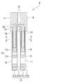
本実施形態の圧電振動子1は、図1から図5に示すように、ベース基板2とリッド基板3とで2層に積層された箱状に形成されており、内部のキャビティC内に圧電振動片4が収容された表面実装型の圧電振動子である。
なお、図5においては、図面を見易くするために後述する励振電極15、引き出し電極19、20、マウント電極16、17及び重り金属膜21の図示を省略している。Hereinafter, embodiments of a piezoelectric vibrator according to the present invention will be described with reference to FIGS. 1 to 13.
As shown in FIGS. 1 to 5, the
In FIG. 5, the
圧電振動片4は、図6から図8に示すように、水晶、タンタル酸リチウムやニオブ酸リチウム等の圧電材料から形成された音叉型の振動片であり、所定の電圧が印加されたときに振動するものである。
この圧電振動片4は、平行に配置された一対の振動腕部10、11と、この一対の振動腕部10、11の基端側を一体的に固定する基部12と、一対の振動腕部10、11の外表面上に形成されて一対の振動腕部10、11を振動させる第1の励振電極13と第2の励振電極14とからなる励振電極15と、第1の励振電極13及び第2の励振電極14に電気的に接続されたマウント電極16、17とを有している。
また、本実施形態の圧電振動片4は、一対の振動腕部10、11の両主面上に、この振動腕部10、11の長手方向に沿ってそれぞれ形成された溝部18を備えている。この溝部18は、振動腕部10、11の基端側から略中間付近まで形成されている。The piezoelectric vibrating
The piezoelectric vibrating
In addition, the piezoelectric vibrating
第1の励振電極13と第2の励振電極14とからなる励振電極15は、一対の振動腕部10、11を互いに接近又は離間する方向に所定の共振周波数で振動させる電極であり、一対の振動腕部10、11の外表面に、それぞれ電気的に切り離された状態でパターニングされて形成されている。具体的には、図8に示すように、第1の励振電極13が、一方の振動腕部10の溝部18上と他方の振動腕部11の両側面上とに主に形成され、第2の励振電極14が、一方の振動腕部10の両側面上と他方の振動腕部11の溝部18上とに主に形成されている。
The
また、第1の励振電極13及び第2の励振電極14は、図6及び図7に示すように、基部12の両主面上において、それぞれ引き出し電極19、20を介してマウント電極16、17に電気的に接続されている。そして圧電振動片4は、このマウント電極16、17を介して電圧が印加されるようになっている。
なお、上述した励振電極15、マウント電極16、17及び引き出し電極19、20は、例えば、クロム(Cr)、ニッケル(Ni)、アルミニウム(Al)やチタン(Ti)等の導電性膜の被膜により形成されたものである。Further, as shown in FIGS. 6 and 7, the
The
また、一対の振動腕部10、11の先端には、自身の振動状態を所定の周波数の範囲内で振動するように調整(周波数調整)を行うための重り金属膜21が被膜されている。なお、この重り金属膜21は、周波数を粗く調整する際に使用される粗調膜21aと、微小に調整する際に使用される微調膜21bとに分かれている。これら粗調膜21a及び微調膜21bを利用して周波数調整を行うことで、一対の振動腕部10、11の周波数をデバイスの公称周波数の範囲内に収めることができる。
A
このように構成された圧電振動片4は、図3及び図5に示すように、金等のバンプBを利用して、ベース基板2の上面にバンプ接合されている。詳しく説明すると、ベース基板2の上面にパターニングされた後述する引き回し電極(内部電極)36、37上にそれぞれ形成されたバンプB上に、一対のマウント電極16、17がそれぞれ接触した状態でバンプ接合されている。これにより、圧電振動片4は、ベース基板2の上面から浮いた状態で支持されると共に、マウント電極16、17と引き回し電極36、37とがそれぞれ電気的に接続された状態となっている。
As shown in FIGS. 3 and 5, the piezoelectric vibrating
上記リッド基板3は、ガラス材料、例えばソーダ石灰ガラスからなる透明の絶縁基板であり、図1、図3及び図5に示すように、板状に形成されている。そして、ベース基板2が接合される接合面側には、圧電振動片4が収まる矩形状の凹部3aが形成されている。この凹部3aは、両基板2、3が重ね合わされたときに、圧電振動片4を収容するキャビティCとなるキャビティ用の凹部である。そして、リッド基板3は、この凹部3aをベース基板2側に対向させた状態でベース基板2に対して陽極接合されている。
The lid substrate 3 is a transparent insulating substrate made of a glass material, for example, soda-lime glass, and is formed in a plate shape as shown in FIGS. A
上記ベース基板2は、リッド基板3と同様にガラス材料、例えばソーダ石灰ガラスからなる透明な絶縁基板であり、図1から図3及び図5に示すように、リッド基板3に対して重ね合わせ可能な大きさで板状に形成されている。
ベース基板2には、このベース基板2を上下方向に貫通するように形成された一対の貫通電極32、33が、それぞれの一端がキャビティC内に収まるように形成されている。
この貫通電極32、33は、ベース基板2との間に隙間なく形成されて、キャビティC内の気密を維持していると共に、後述する外部電極38、39と引き回し電極36、37とを導通させる。The
The
The through-
ベース基板2の上面側(リッド基板3が接合される接合面側)には、図1から図5に示すように、キャビティC内に形成され、加熱されることでキャビティC内の真空度を向上させる金属材料からなるゲッター材34と、陽極接合用の接合膜35と、一対の引き回し電極36、37とがパターニングされている。このうち接合膜35は、例えばアルミニウム等の導電性材料からなり、リッド基板3に形成された凹部3aの周囲を囲むようにベース基板2の周縁に沿って形成されている。
As shown in FIGS. 1 to 5, the upper surface side of the base substrate 2 (the bonding surface side to which the lid substrate 3 is bonded) is formed in the cavity C and heated to reduce the degree of vacuum in the cavity C.
ゲッター材34は、クロム若しくはクロムを主成分とする金属材料で形成されている。本実施形態では、図4に示すように、ゲッター材34は、ベース基板2上に成膜されたクロムからなる下地層34aと、下地層34aに積層された金からなる仕上層34bとを備えている。また、図2に示すように、平面視において圧電振動片4を挟んで両側に対向配置されるように2つ形成されている。また、各々のゲッター材34は、振動腕部10、11に対して、平面視において隣接すると共に平行に延在するように形成されている。
The
一対の引き回し電極36、37は、ゲッター材34と同じ材料で、ゲッター材34と同時に形成されたものである。本実施形態では、図4に示すように、各々の引き回し電極36、37は、ベース基板2上に成膜されたクロムからなる下地層37aと、下地層37aに積層された金からなる仕上層37bとを備えている。また、一対の引き回し電極36、37は、一方の引き回し電極36が、一方の貫通電極32と圧電振動片4の一方のマウント電極16とを電気的に接続すると共に、他方の引き回し電極37が、他方の貫通電極33と圧電振動片4の他方のマウント電極17とを電気的に接続するようにパターニングされている。
The pair of lead-out
また、ベース基板2の下面には、図1、図3及び図5に示すように、一対の貫通電極32、33に対してそれぞれ電気的に接続される外部電極38、39が形成されている。つまり、一方の外部電極38は、一方の貫通電極32及び一方の引き回し電極36を介して圧電振動片4の第1の励振電極13に電気的に接続されている。また、他方の外部電極39は、他方の貫通電極33及び他方の引き回し電極37を介して、圧電振動片4の第2の励振電極14に電気的に接続されている。この結果、一対の励振電極15が、それぞれキャビティCの外部と電気的に接続可能な状態となっている。
Further, as shown in FIGS. 1, 3, and 5,
このように構成された圧電振動子1を動作させる場合には、ベース基板2に形成された外部電極38、39に対して、所定の駆動電圧を印加する。これにより、圧電振動片4の第1の励振電極13及び第2の励振電極14からなる励振電極15に電流を流すことができ、一対の振動腕部10、11を接近・離間させる方向に所定の周波数で振動させることができる。そして、この一対の振動腕部10、11の振動を利用して、時刻源、制御信号のタイミング源やリファレンス信号源等として利用することができる。
When the
次に、上述した圧電振動子1を、図9に示すフローチャートを参照しながら、ベース基板用ウエハ(ベース基板)40とリッド基板用ウエハ(リッド基板)50とを利用して一度に複数製造する製造方法について以下に説明する。なお、本実施形態では、ウエハ状の基板を利用して圧電振動子1を一度に複数製造するが、これに限られたものではなく、予めベース基板2及びリッド基板3の外形に寸法を合わせたものを加工して、一度に一つのみ製造する等しても構わない。
Next, a plurality of the
始めに、圧電振動片作製工程として、図6から図8に示す圧電振動片4を作製する(S10)。具体的には、まず水晶のランバート原石を所定の角度でスライスして一定の厚みのウエハとする。次に、このウエハをラッピングして粗加工した後、加工変質層をエッチングで取り除き、その後ポリッシュ等の鏡面研磨加工を行って、所定の厚みのウエハとする。次に、ウエハに洗浄等の適切な処理を施した後、このウエハをフォトリソグラフィ技術によって圧電振動片4の外形形状でパターニングすると共に、金属膜の成膜及びパターニングを行って、励振電極15、引き出し電極19、20、マウント電極16、17、重り金属膜21を形成する。これにより、複数の圧電振動片4を作製することができる。
First, as a piezoelectric vibrating piece manufacturing step, the piezoelectric vibrating
また、圧電振動片4を作製した後、共振周波数の粗調を行っておく。これは、重り金属膜21の粗調膜21aにレーザ光を照射して一部を蒸発させ、重量を変化させることで行う。なお、共振周波数をより高精度に調整する微調に関しては、マウント後に行う。これについては、後に説明する。
Further, after the piezoelectric vibrating
次に、圧電振動片作製工程と同時或いは前後のタイミングで、第1のウエハ作製工程として、後にリッド基板3となるリッド基板用ウエハ50を、陽極接合を行う直前の状態まで作製する(S20)。まず、ソーダ石灰ガラスを所定の厚みまで研磨加工して洗浄した後に、エッチング等により最表面の加工変質層を除去した円板状のリッド基板用ウエハ50を形成する(S21)。次いで、凹部形成工程として、図10に示すように、リッド基板用ウエハ50の接合面に、エッチング等により行列方向にキャビティ用の凹部3aを複数形成する(S22)。この時点で、第1のウエハ作製工程が終了する。
Next, at the same time as or before and after the piezoelectric vibrating reed manufacturing process, as a first wafer manufacturing process, a
次に、第1のウエハ作製工程と同時或いは前後のタイミングで、第2のウエハ作製工程として、後にベース基板2となるベース基板用ウエハ40を、陽極接合を行う直前の状態まで作製する(S30)。まず、リッド基板用ウエハ50と同様に、ソーダ石灰ガラスを所定の厚みまで研磨加工して洗浄した後に、エッチング等により最表面の加工変質層を除去した円板状のソーダ石灰ガラスからベース基板用ウエハ40を形成する(S31)。
Next, at the same time as or before or after the first wafer fabrication process, as a second wafer fabrication process, a
次に、貫通電極形成工程として、ベース基板用ウエハ40に一対の貫通電極32、33を複数形成する(S32)。この際、例えば、ベース基板用ウエハ40を上下方向に貫通する一対のスルーホールをサンドブラスト法やプレス加工等の方法で複数形成した後、これら複数のスルーホール内に一対の貫通電極32、33を形成する。この一対の貫通電極32、33により、ベース基板用ウエハ40の上面側と下面側との導電性が確保される。
Next, as a through electrode forming step, a plurality of pairs of through
次に、ゲッター材形成工程として、ゲッター材34を形成する(S33)のと同時に、引き回し電極形成工程として、引き回し電極36、37を形成する(S34)。この際、例えば、まずクロムからなる下地層34a、37aをパターニングした後、この下地層34a、37aの上に金からなる仕上層34b、37bとを積層するようにパターニングすることで行う。また、下地層34aをパターニングする際、後に圧電振動片4がベース基板用ウエハ40にマウントされたときに、平面視において圧電振動片4を挟んで両側に対向配置するように2つ形成すると共に、各々のゲッター材34を、振動腕部10、11に対して、平面視において隣接すると共に平行に延在するように形成する。
特に、引き回し電極36、37をゲッター材34と同時に形成するので、圧電振動子1をより効率良く製造することができる。しかも、引き回し電極36、37の仕上層37bとして金を用いているので、引き回し電極36、37の導電性を安定に確保することができ、圧電振動子1の高品質化を図ることができる。Next, the
In particular, since the lead-out
次に、接合膜形成工程として、ベース基板用ウエハ40の上面に導電性材料をパターニングして、図11及び図12に示すように、接合膜35を形成する(S35)。なお、図11及び図12に示す点線Mは、後に行う切断工程で切断する切断線を図示している。また、図12では、図面の見易さのため、接合膜35の図示を省略している。
この時点で第2のウエハ作製工程が終了する。Next, as a bonding film forming step, a conductive material is patterned on the upper surface of the
At this point, the second wafer manufacturing process is completed.
次に、マウント工程として、作製した複数の圧電振動片4を、それぞれ引き回し電極36、37を介してベース基板用ウエハ40の上面に接合する(S40)。この際、まず一対の引き回し電極36、37上にそれぞれ金等のバンプBを形成する。そして、圧電振動片4の基部12をバンプB上に載置した後、バンプBを所定温度(例えば300℃)に加熱しながら圧電振動片4をバンプBに押し付ける。これにより、圧電振動片4は、バンプBに機械的に支持されると共に、マウント電極16、17と引き回し電極36、37とが電気的に接続された状態となる。よって、この時点で圧電振動片4の一対の励振電極15は、一対の貫通電極32、33に対してそれぞれ導通した状態となる。
Next, as a mounting step, the produced plurality of piezoelectric vibrating
圧電振動片4のマウントが終了した後、重ね合わせ工程として、ベース基板用ウエハ40に対してリッド基板用ウエハ50を重ね合わせる(S50)。具体的には、図示しない基準マーク等を指標としながら、両ウエハ40、50を正しい位置にアライメントする。これにより、圧電振動片4、ゲッター材34及び引き回し電極36、37が、ベース基板用ウエハ40に形成された凹部3aと両ウエハ40、50とで囲まれるキャビティC内に収容された状態となる。
After the mounting of the piezoelectric vibrating
重ね合わせ工程後、接合工程として、重ね合わせた2枚のウエハ40、50を図示しない陽極接合装置に入れ、所定の温度雰囲気で所定の電圧を印加して陽極接合する(S60)。具体的には、接合膜35とリッド基板用ウエハ50との間に所定の電圧を印加する。すると、接合膜35とリッド基板用ウエハ50との界面に電気化学的な反応が生じ、両者がそれぞれ強固に密着して陽極接合される。これにより、圧電振動片4をキャビティC内に封止することができ、ベース基板用ウエハ40とリッド基板用ウエハ50とが接合した図13に示すウエハ体60を得ることができる。なお、図13においては、図面を見易くするために、ウエハ体60を分解した状態を図示しており、ベース基板用ウエハ40から接合膜35の図示を省略している。なお、図13に示す点線Mは、後に行う切断工程で切断する切断線を図示している。
After the superposition process, as a joining process, the two
次に、外部電極形成工程として、ベース基板用ウエハ40の下面に導電性材料をパターニングして、一対の貫通電極32、33にそれぞれ電気的に接続された一対の外部電極38、39を複数形成する(S70)。この工程により、外部電極38、39を利用してキャビティC内に収容された圧電振動片4を動作させることができる。
Next, as an external electrode forming step, a conductive material is patterned on the lower surface of the
次に、ゲッタリング工程として、ウエハ体60の各キャビティC内に収容されたゲッター材34を加熱してキャビティC内の真空度を調整する(S80)。具体的には、ウエハ体60を、図示しないゲッタリング調整機にセットして、ゲッタリング調整機内で外部電極38、39に所定の電圧を印加して圧電振動片4を振動させ、等価抵抗値と比例関係にある直列振動抵抗値を測定する。この直列振動抵抗値に基づいて、例えばベース基板用ウエハ40側からレーザを照射することでゲッター材34を加熱して、ゲッタリングを適正回数行う。
なお、ゲッタリングの適正回数の判断方法としては、例えば、圧電振動子の種類ごとに直列振動抵抗値の閾値を予め設定しておき、この閾値を下回った際に適正と判断する方法としてもよい。また、ゲッタリング直前の直列振動抵抗値を記憶してからゲッタリングを行い、ゲッタリング直後の直列振動抵抗値との変化の割合を算出し、この変化の割合を予め設定した値と比較することで判断してもよい。Next, as a gettering step, the
As a method of determining the appropriate number of gettering operations, for example, a threshold value of the series vibration resistance value may be set in advance for each type of piezoelectric vibrator, and may be determined to be appropriate when the threshold value is exceeded. . Also, gettering is performed after storing the series vibration resistance value immediately before gettering, calculating the rate of change from the series vibration resistance value immediately after gettering, and comparing the rate of change with a preset value. You may judge by.
次に、ウエハ体60の状態で、微調工程として、キャビティC内に収容された個々の圧電振動片4の周波数を微調整して所定の範囲内に収める(S90)。具体的に説明すると、ベース基板用ウエハ40の下面に形成された一対の外部電極38、39に電圧を印加して圧電振動片4を振動させる。そして、周波数を計測しながらベース基板用ウエハ40を通して外部からレーザ光を照射し、重り金属膜21の微調膜21bを蒸発させる。これにより、一対の振動腕部10、11の先端側の重量が変化するので、圧電振動片4の周波数を、公称周波数の所定範囲内に収まるように微調整することができる。
Next, in the state of the
周波数の微調が終了した後、切断工程として、接合されたウエハ体60を図13に示す切断線Mに沿って切断して小片化する(S100)。その結果、互いに接合されたベース基板2とリッド基板3との間に形成されたキャビティC内に圧電振動片4が収容された、図1に示す2層構造式表面実装型の圧電振動子1を一度に複数製造することができる。
なお、切断工程(S100)を行って個々の圧電振動子1に小片化した後に、微調工程(S90)を行う工程順序でも構わない。但し、上述したように、微調工程(S90)を先に行うことで、ウエハ体60の状態で微調を行うことができるので、複数の圧電振動子1をより効率良く微調することができる。よって、スループットの向上化を図ることができるので好ましい。After the fine adjustment of the frequency is completed, as a cutting process, the bonded
In addition, after performing the cutting process (S100) and dividing into individual
その後、内部の電気特性検査を行う(S110)。即ち、圧電振動片4の共振周波数、共振抵抗値、ドライブレベル特性(共振周波数及び共振抵抗値の励振電力依存性)等を測定してチェックする。また、絶縁抵抗特性等を併せてチェックする。そして、最後に圧電振動子1の外観検査を行って、寸法や品質等を最終的にチェックする。これをもって圧電振動子1の製造が終了する。
Thereafter, an internal electrical characteristic inspection is performed (S110). That is, the resonance frequency, resonance resistance value, drive level characteristic (excitation power dependency of the resonance frequency and resonance resistance value) and the like of the piezoelectric vibrating
特に、ゲッター材34がクロムからなる下地層34aを備えているので、高い耐食性を発揮させることができる。つまり、クロムはアルミニウムと比べて耐食性により優れているので、アルミニウムで形成していた従来の場合に比べて、ゲッター材34の耐食性をより向上することができる。このため、この圧電振動子1を仮に高湿度の環境下で使用したとしても、ゲッター材34が腐食し難い。よって、腐食に起因する品質低下や特性変化を招きにくい。よって、動作の信頼性を向上させることができる。
しかも、クロムは耐食性が優れている上に、酸素と結合し易いので、ゲッタリング工程の際、ゲッター材34が加熱されて蒸発したときに主に酸素からなるキャビティC内のガスを吸収し易く、ゲッタリング効果が高い。つまり、アルミニウムで形成していた従来のゲッター材と同等或いはそれ以上のゲッタリング効果を期待することができる。このため、キャビティC内の真空度を依然として短時間で向上させることができるので、圧電振動子1を効率良く製造することができる。In particular, since the
Moreover, chromium is excellent in corrosion resistance and easily binds to oxygen. Therefore, in the gettering process, when the
また、ゲッター材34は、圧電振動片4ではなく、ベース基板用ウエハ40(ベース基板2)に形成されている。従って、ゲッタリング工程の際、ゲッター材34をレーザ等で加熱しても、圧電振動片4に対して加熱の影響を何ら与えることがない。よって、圧電振動片4に対して加熱による負荷を与えることがない。このため、圧電振動子1の品質や特性に何ら影響を与えることがないので、圧電振動子1の高品質化を図ることができる。
Further, the
次に、本発明に係る発振器の一実施形態について、図14を参照しながら説明する。
本実施形態の発振器100は、図14に示すように、圧電振動子1を、集積回路101に電気的に接続された発振子として構成したものである。この発振器100は、コンデンサ等の電子部品102が実装された基板103を備えている。基板103には、発振器用の上記集積回路101が実装されており、この集積回路101の近傍に、圧電振動子1が実装されている。これら電子部品102、集積回路101及び圧電振動子1は、図示しない配線パターンによってそれぞれ電気的に接続されている。なお、各構成部品は、図示しない樹脂によりモールドされている。Next, an embodiment of an oscillator according to the present invention will be described with reference to FIG.
As shown in FIG. 14, the
このように構成された発振器100において、圧電振動子1に電圧を印加すると、この圧電振動子1内の圧電振動片4が振動する。この振動は、圧電振動片4が有する圧電特性により電気信号に変換されて、集積回路101に電気信号として入力される。入力された電気信号は、集積回路101によって各種処理がなされ、周波数信号として出力される。これにより、圧電振動子1が発振子として機能する。
また、集積回路101の構成を、例えば、RTC(リアルタイムクロック)モジュール等を要求に応じて選択的に設定することで、時計用単機能発振器等の他、当該機器や外部機器の動作日や時刻を制御したり、時刻やカレンダー等を提供したりする機能を付加することができる。In the
In addition, by selectively setting the configuration of the
上述したように、本実施形態の発振器100によれば、動作の信頼性が向上された上に高品質な圧電振動子1を備えているので、発振器100自体も同様に動作の信頼性を高めて高品質化を図ることができる。さらにこれに加え、長期にわたって安定した高精度な周波数信号を得ることができる。
As described above, according to the
次に、本発明に係る電子機器の一実施形態について、図15を参照して説明する。なお電子機器として、上述した圧電振動子1を有する携帯情報機器110を例にして説明する。始めに本実施形態の携帯情報機器110は、例えば、携帯電話に代表されるものであり、従来技術における腕時計を発展、改良したものである。外観は腕時計に類似し、文字盤に相当する部分に液晶ディスプレイを配し、この画面上に現在の時刻等を表示させることができるものである。また、通信機として利用する場合には、手首から外し、バンドの内側部分に内蔵されたスピーカ及びマイクロフォンによって、従来技術の携帯電話と同様の通信を行うことが可能である。しかしながら、従来の携帯電話と比較して、格段に小型化及び軽量化されている。
Next, an embodiment of an electronic apparatus according to the present invention will be described with reference to FIG. Note that the
次に、本実施形態の携帯情報機器110の構成について説明する。この携帯情報機器110は、図15に示すように、圧電振動子1と、電力を供給するための電源部111とを備えている。電源部111は、例えば、リチウム二次電池からなっている。この電源部111には、各種制御を行う制御部112と、時刻等のカウントを行う計時部113と、外部との通信を行う通信部114と、各種情報を表示する表示部115と、それぞれの機能部の電圧を検出する電圧検出部116とが並列に接続されている。そして、電源部111によって、各機能部に電力が供給されるようになっている。
Next, the configuration of the
制御部112は、各機能部を制御して音声データの送信及び受信、現在時刻の計測や表示等、システム全体の動作制御を行う。また、制御部112は、予めプログラムが書き込まれたROMと、このROMに書き込まれたプログラムを読み出して実行するCPUと、このCPUのワークエリアとして使用されるRAM等とを備えている。
The
計時部113は、発振回路、レジスタ回路、カウンタ回路及びインターフェース回路等を内蔵する集積回路と、圧電振動子1とを備えている。圧電振動子1に電圧を印加すると圧電振動片4が振動し、この振動が水晶の有する圧電特性により電気信号に変換されて、発振回路に電気信号として入力される。発振回路の出力は二値化され、レジスタ回路とカウンタ回路とにより計数される。そして、インターフェース回路を介して、制御部112と信号の送受信が行われ、表示部115に、現在時刻や現在日付或いはカレンダー情報等が表示される。
The
通信部114は、従来の携帯電話と同様の機能を有し、無線部117、音声処理部118、切替部119、増幅部120、音声入出力部121、電話番号入力部122、着信音発生部123及び呼制御メモリ部124を備えている。
無線部117は、音声データ等の各種データを、アンテナ125を介して基地局と送受信のやりとりを行う。音声処理部118は、無線部117又は増幅部120から入力された音声信号を符号化及び複号化する。増幅部120は、音声処理部118又は音声入出力部121から入力された信号を、所定のレベルまで増幅する。音声入出力部121は、スピーカやマイクロフォン等からなり、着信音や受話音声を拡声したり、音声を集音したりする。The
The
また、着信音発生部123は、基地局からの呼び出しに応じて着信音を生成する。切替部119は、着信時に限って、音声処理部118に接続されている増幅部120を着信音発生部123に切り替えることによって、着信音発生部123において生成された着信音が増幅部120を介して音声入出力部121に出力される。
なお、呼制御メモリ部124は、通信の発着呼制御に係るプログラムを格納する。また、電話番号入力部122は、例えば、0から9の番号キー及びその他のキーを備えており、これら番号キー等を押下することにより、通話先の電話番号等が入力される。In addition, the
The call
電圧検出部116は、電源部111によって制御部112等の各機能部に対して加えられている電圧が、所定の値を下回った場合に、その電圧降下を検出して制御部112に通知する。このときの所定の電圧値は、通信部114を安定して動作させるために必要な最低限の電圧として予め設定されている値であり、例えば、3V程度となる。電圧検出部116から電圧降下の通知を受けた制御部112は、無線部117、音声処理部118、切替部119及び着信音発生部123の動作を禁止する。特に、消費電力の大きな無線部117の動作停止は、必須となる。更に、表示部115に、通信部114が電池残量の不足により使用不能になった旨が表示される。
When the voltage applied to each functional unit such as the
即ち、電圧検出部116と制御部112とによって、通信部114の動作を禁止し、その旨を表示部115に表示することができる。この表示は、文字メッセージであっても良いが、より直感的な表示として、表示部115の表示面の上部に表示された電話アイコンに、×(バツ)印を付けるようにしても良い。
なお、通信部114の機能に係る部分の電源を、選択的に遮断することができる電源遮断部126を備えることで、通信部114の機能をより確実に停止することができる。That is, the operation of the
In addition, the function of the
上述したように、本実施形態の携帯情報機器110によれば、動作の信頼性が向上された上に高品質な圧電振動子1を備えているので、携帯情報機器自体も同様に動作の信頼性を高めて高品質化を図ることができる。さらにこれに加え、長期にわたって安定した高精度な時計情報を表示することができる。
As described above, according to the
次に、本発明に係る電波時計の一実施形態について、図16を参照して説明する。
本実施形態の電波時計130は、図16に示すように、フィルタ部131に電気的に接続された圧電振動子1を備えたものであり、時計情報を含む標準の電波を受信して、正確な時刻に自動修正して表示する機能を備えた時計である。
日本国内には、福島県(40kHz)と佐賀県(60kHz)とに、標準の電波を送信する送信所(送信局)があり、それぞれ標準電波を送信している。40kHz若しくは60kHzのような長波は、地表を伝播する性質と、電離層と地表とを反射しながら伝播する性質とを併せもつため、伝播範囲が広く、上述した2つの送信所で日本国内を全て網羅している。Next, an embodiment of a radio timepiece according to the present invention will be described with reference to FIG.
As shown in FIG. 16, the
In Japan, there are transmitting stations (transmitting stations) that transmit standard radio waves in Fukushima Prefecture (40 kHz) and Saga Prefecture (60 kHz), each transmitting standard radio waves. Long waves such as 40 kHz or 60 kHz have the property of propagating the surface of the earth and the property of propagating while reflecting the ionosphere and the surface of the earth, so the propagation range is wide, and the above two transmitting stations cover all of Japan. doing.
以下、電波時計130の機能的構成について詳細に説明する。
アンテナ132は、40kHz若しくは60kHzの長波の標準電波を受信する。長波の標準電波は、タイムコードと呼ばれる時刻情報を、40kHz若しくは60kHzの搬送波にAM変調をかけたものである。受信された長波の標準電波は、アンプ133によって増幅され、複数の圧電振動子1を有するフィルタ部131によって濾波、同調される。
本実施形態における圧電振動子1は、上記搬送周波数と同一の40kHz及び60kHzの共振周波数を有する水晶振動子部138、139をそれぞれ備えている。Hereinafter, the functional configuration of the
The
The
更に、濾波された所定周波数の信号は、検波、整流回路134により検波復調される。次に、波形整形回路135を介してタイムコードが取り出され、CPU136でカウントされる。CPU136では、現在の年、積算日、曜日、時刻等の情報を読み取る。読み取られた情報は、RTC137に反映され、正確な時刻情報が表示される。
搬送波は、40kHz若しくは60kHzであるから、水晶振動子部138、139は、上述した音叉型の構造を持つ振動子が好適である。Further, the filtered signal having a predetermined frequency is detected and demodulated by the detection and
Since the carrier wave is 40 kHz or 60 kHz, the
なお、上述の説明は、日本国内の例で示したが、長波の標準電波の周波数は、海外では異なっている。例えば、ドイツでは77.5KHzの標準電波が用いられている。従って、海外でも対応可能な電波時計130を携帯機器に組み込む場合には、さらに日本の場合とは異なる周波数の圧電振動子1を必要とする。
In addition, although the above-mentioned description was shown in the example in Japan, the frequency of the long standard wave is different overseas. For example, in Germany, a standard radio wave of 77.5 KHz is used. Accordingly, when the
上述したように、本実施形態の電波時計130によれば、動作の信頼性が向上された上に高品質な圧電振動子1を備えているので、電波時計自体も同様に動作の信頼性を高めて高品質化を図ることができる。さらにこれに加え、長期にわたって安定して高精度に時刻をカウントすることができる。
As described above, according to the
なお、本発明の技術的範囲は上記実施形態に限定されるものではなく、本発明の趣旨を逸脱しない範囲において種々の変更を加えることが可能である。 The technical scope of the present invention is not limited to the above embodiment, and various modifications can be made without departing from the spirit of the present invention.
例えば、上記実施形態では、ゲッター材34が、ベース基板2(ベース基板用ウエハ40)上に形成されているものとしたが、キャビティC内に形成されていれば、例えばリッド基板3(リッド基板用ウエハ50)上に形成されていても構わないし、圧電振動片4の表面に形成されていても構わない。
また、上記実施形態では、ゲッター材34が、平面視において圧電振動片4を挟んで両側に対向配置されるように2つ形成されているとしたが、例えば平面視において圧電振動片4の外側一方にのみ隣接して形成されていても構わない。For example, in the above embodiment, the
In the above embodiment, two
また、上記実施形態では、ゲッター材34が、下地層34aと仕上層34bとを備えるものとしたが、例えば、クロムの下地層34aでのみ形成されていても良い。また、ゲッター材34として、クロムを主成分とする合金を用いても構わない。
また、上記実施形態では、ゲッター材形成工程と引き回し電極形成工程とを同時に行うものとしたが、別々のタイミングに行っても構わない。In the above embodiment, the
In the above embodiment, the getter material forming step and the lead-out electrode forming step are performed at the same time, but may be performed at different timings.
また、上記実施形態では、圧電振動片4の一例として振動腕部10、11の両面に溝部18が形成された溝付きの圧電振動片4を例に挙げて説明したが、溝部18がないタイプの圧電振動片でも構わない。但し、溝部18を形成することで、一対の励振電極15に所定の電圧を印加させたときに、一対の励振電極15間における電界効率を上げることができるので、振動損失をより抑えて振動特性をさらに向上することができる。つまり、CI値(Crystal Impedance)をさらに低くすることができ、圧電振動片4の更なる高性能化を図ることができる。この点において、溝部18を形成する方が好ましい。
また、上記実施形態では、音叉型の圧電振動片4を例に挙げて説明したが、音叉型に限られるものではない。例えば、厚み滑り振動片としても構わない。In the above-described embodiment, as an example of the piezoelectric vibrating
In the above embodiment, the tuning fork type
また、上記実施形態では、ベース基板2とリッド基板3とを接合膜35を介して陽極接合したが、陽極接合に限定されるものではない。但し、陽極接合することで、両基板2、3を強固に接合できるので好ましい。
また、上記実施形態では、圧電振動片4をバンプ接合したが、バンプ接合に限定されるものではない。例えば、導電性接着剤により圧電振動片4を接合しても構わない。但し、バンプ接合することで、圧電振動片4をベース基板2の上面から浮かすことができ、振動に必要な最低限の振動ギャップを自然と確保することができる。よって、バンプ接合することが好ましい。In the above embodiment, the
In the above embodiment, the piezoelectric vibrating
その他、本発明の趣旨に逸脱しない範囲で、上記実施形態における構成要素を周知の構成要素に置き換えることは適宜可能であり、また、上記した変形例を適宜組み合わせてもよい。 In addition, it is possible to appropriately replace the constituent elements in the above-described embodiments with well-known constituent elements without departing from the spirit of the present invention, and the above-described modified examples may be appropriately combined.
次に、本発明に係る圧電振動子及び従来の圧電振動子にそれぞれ所定の電圧を印加して振動させ、等価抵抗値Reと比例関係にある直列共振抵抗値R1(以下、単にR1値と称する)を計測した結果を以下に示す。なお、前述のように等価抵抗値Reはキャビティ内の真空度と反比例関係にあるので、R1値もキャビティ内の真空度と反比例関係にあり、R1値が低いほどキャビティ内の真空度が高いことになる。
ここで、計測を行うにあたって、本発明に係る圧電振動子としては、ゲッター材がクロムのみで形成され、このゲッター材の厚みが600Åのものを用いた。また、従来の圧電振動子としては、ゲッター材がアルミニウムのみで形成され、このゲッター材の厚みが1100Åのものを用いた。つまり、本発明に係る圧電振動子のゲッター材には、従来の圧電振動子のゲッター材より厚みが薄いものを用いた。
そして、本発明に係る圧電振動子及び従来の圧電振動子について、このゲッター材の構成以外の点において条件を合わせて、それぞれの圧電振動子を同じ回数だけゲッタリングし、ゲッタリング前後のR1値を比較した。Next, a predetermined voltage is applied to the piezoelectric vibrator according to the present invention and the conventional piezoelectric vibrator to vibrate, and a series resonance resistance value R1 (hereinafter simply referred to as R1 value) proportional to the equivalent resistance value Re. ) Is shown below. Since the equivalent resistance value Re is inversely proportional to the degree of vacuum in the cavity as described above, the R1 value is also inversely proportional to the degree of vacuum in the cavity. The lower the R1 value, the higher the degree of vacuum in the cavity. become.
Here, when performing the measurement, a piezoelectric vibrator according to the present invention was used in which the getter material was formed only of chromium and the getter material had a thickness of 600 mm. Further, as a conventional piezoelectric vibrator, a getter material made of only aluminum and having a thickness of 1100 mm was used. That is, the getter material of the piezoelectric vibrator according to the present invention is thinner than the getter material of the conventional piezoelectric vibrator.
Then, for the piezoelectric vibrator according to the present invention and the conventional piezoelectric vibrator, conditions are obtained except for the configuration of the getter material, each piezoelectric vibrator is gettered the same number of times, and R1 values before and after gettering are obtained. Compared.
比較の結果を図17の表に示す。図17の表は、従来の圧電振動子(Al(1100Å)及び本発明に係る圧電振動子(Cr(600Å))のそれぞれについて、ゲッタリング前後のR1値(ゲッタリング前(KΩ):A、ゲッタリング後(KΩ):B)、及びゲッタリング前後のR1値の減少量(減少量(KΩ):A−B)を示した表である。
この結果によれば、本発明に係る圧電振動子では、ゲッター材の厚みが従来の圧電振動子のゲッター材の厚みより薄いにも関わらず、従来のものよりゲッタリング前後のR1値の減少量が大きいことが確認できた。つまり、ゲッター材をクロムで形成することで、アルミニウムで形成する従来の場合以上のゲッタリング効果を得ることができるのを確認できた。The comparison results are shown in the table of FIG. The table of FIG. 17 shows the R1 value before and after gettering (before gettering (KΩ): A, for each of the conventional piezoelectric vibrator (Al (1100Å) and the piezoelectric vibrator (Cr (600Å)) according to the present invention. It is the table | surface which showed the reduction | decrease amount (reduction amount (Kohm): AB) of R1 value after gettering (Kohm): B) and before and after gettering.
According to this result, in the piezoelectric vibrator according to the present invention, although the thickness of the getter material is thinner than the thickness of the getter material of the conventional piezoelectric vibrator, the decrease amount of the R1 value before and after the gettering than the conventional one. Was confirmed to be large. That is, it has been confirmed that by forming the getter material with chromium, it is possible to obtain a gettering effect higher than that of the conventional case of forming with aluminum.
Claims (5)
前記ゲッター材を、クロム若しくはクロムを主成分とする金属材料で形成すると共に、前記内部電極を、前記ゲッター材と同じ材料で、前記ゲッター材と同時に形成することを特徴とする圧電振動子の製造方法。A base substrate and a lid substrate bonded to each other and having a cavity formed therebetween, an external electrode formed on the lower surface of the base substrate, and an interior formed on the upper surface of the base substrate so as to be accommodated in the cavity An electrode, a through electrode that is formed so as to penetrate the base substrate, and electrically connected to the external electrode and the internal electrode, and is accommodated in the cavity in a state of being electrically connected to the internal electrode. A piezoelectric vibrator comprising: a piezoelectric vibrating piece; and a getter material formed on an upper surface of the base substrate in the cavity,
The getter material is made of chromium or a metal material mainly composed of chromium, and the internal electrode is made of the same material as the getter material and is formed simultaneously with the getter material. Method.
前記ベース基板の下面に形成された外部電極と
前記キャビティ内に収容されるように前記ベース基板の上面に形成された内部電極と
前記ベース基板を貫通するように形成され、前記外部電極と前記内部電極とを電気的に接続する貫通電極と
前記内部電極に電気的に接続された状態で前記キャビティ内に収容された圧電振動片と
クロム若しくはクロムを主成分とする金属材料で前記キャビティ内の前記ベース基板の上面に形成されたゲッター材と
を備え、
前記内部電極は、前記ゲッター材と同じ材料で、前記ゲッター材と同時に形成されたものであることを特徴とする圧電振動子。A base substrate and a lid substrate bonded to each other and having a cavity formed therebetween; an external electrode formed on a lower surface of the base substrate; and an internal electrode formed on an upper surface of the base substrate so as to be received in the cavity A penetrating electrode formed so as to penetrate the base substrate and electrically connecting the external electrode and the internal electrode; and a piezoelectric vibrating piece housed in the cavity while being electrically connected to the internal electrode And a getter material formed on the upper surface of the base substrate in the cavity with chromium or a metal material mainly composed of chromium ,
The piezoelectric vibrator is characterized in that the internal electrode is made of the same material as the getter material and is formed simultaneously with the getter material .
Applications Claiming Priority (1)
| Application Number | Priority Date | Filing Date | Title |
|---|---|---|---|
| PCT/JP2008/065250 WO2010023731A1 (en) | 2008-08-27 | 2008-08-27 | Piezoelectric vibrator, oscillator, electronic apparatus and radio clock, and manufacturing method of piezoelectric vibrator |
Publications (2)
| Publication Number | Publication Date |
|---|---|
| JPWO2010023731A1 JPWO2010023731A1 (en) | 2012-01-26 |
| JP5128671B2 true JP5128671B2 (en) | 2013-01-23 |
Family
ID=41720920
Family Applications (1)
| Application Number | Title | Priority Date | Filing Date |
|---|---|---|---|
| JP2010526453A Expired - Fee Related JP5128671B2 (en) | 2008-08-27 | 2008-08-27 | Piezoelectric vibrator, oscillator, electronic device, radio timepiece, and method for manufacturing piezoelectric vibrator |
Country Status (5)
| Country | Link |
|---|---|
| US (1) | US8514029B2 (en) |
| JP (1) | JP5128671B2 (en) |
| CN (1) | CN102204090A (en) |
| TW (1) | TW201014168A (en) |
| WO (1) | WO2010023731A1 (en) |
Families Citing this family (5)
| Publication number | Priority date | Publication date | Assignee | Title |
|---|---|---|---|---|
| CN102197586B (en) * | 2008-08-27 | 2014-03-05 | 精工电子水晶科技股份有限公司 | Piezoelectric vibrator, oscillator, electronic apparatus and radio clock, and method for manufacturing piezoelectric vibrator |
| JP5129284B2 (en) * | 2010-03-09 | 2013-01-30 | 日本電波工業株式会社 | Piezoelectric vibrator and method for manufacturing the piezoelectric vibrator |
| JP6155551B2 (en) * | 2012-04-10 | 2017-07-05 | セイコーエプソン株式会社 | Electronic device, electronic apparatus, and method for manufacturing electronic device |
| JP2014032137A (en) * | 2012-08-06 | 2014-02-20 | Seiko Epson Corp | Vibration piece, electronic device and electronic apparatus |
| WO2014129666A1 (en) * | 2013-02-25 | 2014-08-28 | 京セラ株式会社 | Package for housing electronic component and electronic device |
Citations (12)
| Publication number | Priority date | Publication date | Assignee | Title |
|---|---|---|---|---|
| JPS53149794A (en) * | 1977-06-01 | 1978-12-27 | Seiko Instr & Electronics Ltd | Piezo-electric vibrator |
| JPH05191190A (en) * | 1992-01-10 | 1993-07-30 | Seiko Epson Corp | Packaging method for piezoelectric element |
| JPH07335777A (en) * | 1994-06-13 | 1995-12-22 | Toshiba Corp | Optical semiconductor device |
| JP2002033569A (en) * | 2000-07-14 | 2002-01-31 | Nippon Dempa Kogyo Co Ltd | Mounting substrate for vibrator and crystal vibrator |
| JP2002121037A (en) * | 2000-08-07 | 2002-04-23 | Nippon Sheet Glass Co Ltd | Method of manufacturing multipiece blank layout glass sheet or electronic parts package |
| JP2004066225A (en) * | 2002-06-13 | 2004-03-04 | Lg Electronics Inc | Getter composition and field emission display apparatus using the getter composition |
| JP2006094154A (en) * | 2004-09-24 | 2006-04-06 | Seiko Epson Corp | Piezoelectric vibration chip and piezoelectric device |
| JP2006121544A (en) * | 2004-10-25 | 2006-05-11 | Seiko Epson Corp | Piezoelectric vibration chip and piezoelectric device |
| JP2007081697A (en) * | 2005-09-13 | 2007-03-29 | Daishinku Corp | Piezoelectric oscillation device and method of manufacturing same |
| JP2007129327A (en) * | 2005-11-01 | 2007-05-24 | Seiko Instruments Inc | Piezoelectric vibrator and oscillator provided with the same, radio clock, and electronic apparatus |
| JP2007184752A (en) * | 2006-01-06 | 2007-07-19 | Seiko Instruments Inc | Piezoelectric vibrator and radio controlled watch equipped with the same, oscillator, and electronic equipment |
| JP2007251238A (en) * | 2006-03-13 | 2007-09-27 | Epson Toyocom Corp | Piezoelectric device and manufacturing method thereof |
Family Cites Families (4)
| Publication number | Priority date | Publication date | Assignee | Title |
|---|---|---|---|---|
| KR100415615B1 (en) * | 2001-06-13 | 2004-01-24 | 엘지전자 주식회사 | Composition Of Getter And Field Emission Display Using The Same |
| JP3998948B2 (en) | 2001-10-31 | 2007-10-31 | セイコーインスツル株式会社 | Piezoelectric vibrator and manufacturing method thereof |
| EP1536559A1 (en) * | 2003-11-25 | 2005-06-01 | ETA SA Manufacture Horlogère Suisse | Electronic device has a resonator element in a hemetically closed case |
| EP1641118B1 (en) * | 2004-09-24 | 2010-04-21 | Seiko Epson Corporation | Piezoelectric resonator element and piezoelectric device |
-
2008
- 2008-08-27 JP JP2010526453A patent/JP5128671B2/en not_active Expired - Fee Related
- 2008-08-27 WO PCT/JP2008/065250 patent/WO2010023731A1/en active Application Filing
- 2008-08-27 CN CN2008801319229A patent/CN102204090A/en active Pending
-
2009
- 2009-07-15 TW TW098123909A patent/TW201014168A/en unknown
-
2011
- 2011-02-25 US US13/035,468 patent/US8514029B2/en not_active Expired - Fee Related
Patent Citations (12)
| Publication number | Priority date | Publication date | Assignee | Title |
|---|---|---|---|---|
| JPS53149794A (en) * | 1977-06-01 | 1978-12-27 | Seiko Instr & Electronics Ltd | Piezo-electric vibrator |
| JPH05191190A (en) * | 1992-01-10 | 1993-07-30 | Seiko Epson Corp | Packaging method for piezoelectric element |
| JPH07335777A (en) * | 1994-06-13 | 1995-12-22 | Toshiba Corp | Optical semiconductor device |
| JP2002033569A (en) * | 2000-07-14 | 2002-01-31 | Nippon Dempa Kogyo Co Ltd | Mounting substrate for vibrator and crystal vibrator |
| JP2002121037A (en) * | 2000-08-07 | 2002-04-23 | Nippon Sheet Glass Co Ltd | Method of manufacturing multipiece blank layout glass sheet or electronic parts package |
| JP2004066225A (en) * | 2002-06-13 | 2004-03-04 | Lg Electronics Inc | Getter composition and field emission display apparatus using the getter composition |
| JP2006094154A (en) * | 2004-09-24 | 2006-04-06 | Seiko Epson Corp | Piezoelectric vibration chip and piezoelectric device |
| JP2006121544A (en) * | 2004-10-25 | 2006-05-11 | Seiko Epson Corp | Piezoelectric vibration chip and piezoelectric device |
| JP2007081697A (en) * | 2005-09-13 | 2007-03-29 | Daishinku Corp | Piezoelectric oscillation device and method of manufacturing same |
| JP2007129327A (en) * | 2005-11-01 | 2007-05-24 | Seiko Instruments Inc | Piezoelectric vibrator and oscillator provided with the same, radio clock, and electronic apparatus |
| JP2007184752A (en) * | 2006-01-06 | 2007-07-19 | Seiko Instruments Inc | Piezoelectric vibrator and radio controlled watch equipped with the same, oscillator, and electronic equipment |
| JP2007251238A (en) * | 2006-03-13 | 2007-09-27 | Epson Toyocom Corp | Piezoelectric device and manufacturing method thereof |
Also Published As
| Publication number | Publication date |
|---|---|
| WO2010023731A1 (en) | 2010-03-04 |
| CN102204090A (en) | 2011-09-28 |
| US8514029B2 (en) | 2013-08-20 |
| JPWO2010023731A1 (en) | 2012-01-26 |
| TW201014168A (en) | 2010-04-01 |
| US20110148539A1 (en) | 2011-06-23 |
Similar Documents
| Publication | Publication Date | Title |
|---|---|---|
| JP5237976B2 (en) | Piezoelectric vibrator, method for manufacturing piezoelectric vibrator, oscillator, electronic device, and radio timepiece | |
| JP5121493B2 (en) | Method for manufacturing piezoelectric vibrator | |
| US8212454B2 (en) | Piezoelectric vibrator, piezoelectric vibrator manufacturing method, oscillator, electronic device, radio-controlled timepiece | |
| JP5226791B2 (en) | Piezoelectric vibrator, oscillator, electronic device, radio timepiece, and method of manufacturing piezoelectric vibrator | |
| JP5237965B2 (en) | Method for manufacturing piezoelectric vibrator | |
| JP5121934B2 (en) | Piezoelectric vibrator manufacturing method, piezoelectric vibrator, oscillator, electronic device, and radio timepiece | |
| JP5226073B2 (en) | Piezoelectric vibrators, oscillators, electronic equipment and radio clocks | |
| JP2011142591A (en) | Method of manufacturing piezoelectric vibrator, oscillator, electronic apparatus and radio wave clock | |
| JP2011029910A (en) | Piezoelectric vibrator, manufacturing method of piezoelectric vibrator, oscillator, electronic device, and radio wave clock | |
| JP2011030095A (en) | Piezoelectric vibrator, method for manufacturing piezoelectric vibrator, oscillator, electronic equipment, and radio wave clock | |
| JP5128670B2 (en) | Piezoelectric vibrator, oscillator, electronic device, radio timepiece, and method for manufacturing piezoelectric vibrator | |
| JP5529463B2 (en) | Package manufacturing method and piezoelectric vibrator manufacturing method | |
| JP5162675B2 (en) | Piezoelectric vibrator manufacturing method, piezoelectric vibrator, oscillator, electronic device, and radio timepiece | |
| JP5128671B2 (en) | Piezoelectric vibrator, oscillator, electronic device, radio timepiece, and method for manufacturing piezoelectric vibrator | |
| JP2012169865A (en) | Piezoelectric vibrating reed, piezoelectric vibrator, oscillator, electronic equipment, and radio clock | |
| JP5128669B2 (en) | Method for manufacturing piezoelectric vibrator | |
| JP5421690B2 (en) | Package manufacturing method | |
| JP2011029911A (en) | Method for manufacturing piezoelectric vibrator, piezoelectric vibrator, oscillator, electronic device, and radio wave clock | |
| WO2010097901A1 (en) | Anodic bonding method, package manufacturing method, piezoelectric vibrator manufacturing method, oscillator, electronic apparatus and radio-controlled clock | |
| JP5827088B2 (en) | Terminal connection structure of electronic parts, package, piezoelectric vibrator, oscillator, electronic equipment and radio clock | |
| JP5184648B2 (en) | Method for manufacturing piezoelectric vibrator | |
| JP2013165396A (en) | Piezoelectric vibration piece, piezoelectric vibrator manufacturing method, piezoelectric vibrator, oscillator, electronic equipment, and radio clock | |
| US20110249534A1 (en) | Package manufacturing method, piezoelectric vibrator manufacturing method, oscillator, electronic device, and radio-controlled timepiece |
Legal Events
| Date | Code | Title | Description |
|---|---|---|---|
| A131 | Notification of reasons for refusal |
Free format text: JAPANESE INTERMEDIATE CODE: A131 Effective date: 20120731 |
|
| A521 | Written amendment |
Free format text: JAPANESE INTERMEDIATE CODE: A523 Effective date: 20120925 |
|
| TRDD | Decision of grant or rejection written | ||
| A01 | Written decision to grant a patent or to grant a registration (utility model) |
Free format text: JAPANESE INTERMEDIATE CODE: A01 Effective date: 20121023 |
|
| A01 | Written decision to grant a patent or to grant a registration (utility model) |
Free format text: JAPANESE INTERMEDIATE CODE: A01 |
|
| A61 | First payment of annual fees (during grant procedure) |
Free format text: JAPANESE INTERMEDIATE CODE: A61 Effective date: 20121031 |
|
| R150 | Certificate of patent or registration of utility model |
Ref document number: 5128671 Country of ref document: JP Free format text: JAPANESE INTERMEDIATE CODE: R150 Free format text: JAPANESE INTERMEDIATE CODE: R150 |
|
| FPAY | Renewal fee payment (event date is renewal date of database) |
Free format text: PAYMENT UNTIL: 20151109 Year of fee payment: 3 |
|
| S111 | Request for change of ownership or part of ownership |
Free format text: JAPANESE INTERMEDIATE CODE: R313111 |
|
| R360 | Written notification for declining of transfer of rights |
Free format text: JAPANESE INTERMEDIATE CODE: R360 |
|
| R370 | Written measure of declining of transfer procedure |
Free format text: JAPANESE INTERMEDIATE CODE: R370 |
|
| S111 | Request for change of ownership or part of ownership |
Free format text: JAPANESE INTERMEDIATE CODE: R313111 |
|
| R350 | Written notification of registration of transfer |
Free format text: JAPANESE INTERMEDIATE CODE: R350 |
|
| R250 | Receipt of annual fees |
Free format text: JAPANESE INTERMEDIATE CODE: R250 |
|
| R250 | Receipt of annual fees |
Free format text: JAPANESE INTERMEDIATE CODE: R250 |
|
| R250 | Receipt of annual fees |
Free format text: JAPANESE INTERMEDIATE CODE: R250 |
|
| R250 | Receipt of annual fees |
Free format text: JAPANESE INTERMEDIATE CODE: R250 |
|
| LAPS | Cancellation because of no payment of annual fees |