JP5134779B2 - Delay synchronization circuit - Google Patents
Delay synchronization circuit Download PDFInfo
- Publication number
- JP5134779B2 JP5134779B2 JP2006067243A JP2006067243A JP5134779B2 JP 5134779 B2 JP5134779 B2 JP 5134779B2 JP 2006067243 A JP2006067243 A JP 2006067243A JP 2006067243 A JP2006067243 A JP 2006067243A JP 5134779 B2 JP5134779 B2 JP 5134779B2
- Authority
- JP
- Japan
- Prior art keywords
- signal
- circuit
- locked loop
- delay
- control
- Prior art date
- Legal status (The legal status is an assumption and is not a legal conclusion. Google has not performed a legal analysis and makes no representation as to the accuracy of the status listed.)
- Expired - Fee Related
Links
Images


Classifications
-
- H—ELECTRICITY
- H03—ELECTRONIC CIRCUITRY
- H03L—AUTOMATIC CONTROL, STARTING, SYNCHRONISATION, OR STABILISATION OF GENERATORS OF ELECTRONIC OSCILLATIONS OR PULSES
- H03L7/00—Automatic control of frequency or phase; Synchronisation
- H03L7/06—Automatic control of frequency or phase; Synchronisation using a reference signal applied to a frequency- or phase-locked loop
- H03L7/08—Details of the phase-locked loop
- H03L7/085—Details of the phase-locked loop concerning mainly the frequency- or phase-detection arrangement including the filtering or amplification of its output signal
- H03L7/089—Details of the phase-locked loop concerning mainly the frequency- or phase-detection arrangement including the filtering or amplification of its output signal the phase or frequency detector generating up-down pulses
- H03L7/0891—Details of the phase-locked loop concerning mainly the frequency- or phase-detection arrangement including the filtering or amplification of its output signal the phase or frequency detector generating up-down pulses the up-down pulses controlling source and sink current generators, e.g. a charge pump
-
- A—HUMAN NECESSITIES
- A23—FOODS OR FOODSTUFFS; TREATMENT THEREOF, NOT COVERED BY OTHER CLASSES
- A23N—MACHINES OR APPARATUS FOR TREATING HARVESTED FRUIT, VEGETABLES OR FLOWER BULBS IN BULK, NOT OTHERWISE PROVIDED FOR; PEELING VEGETABLES OR FRUIT IN BULK; APPARATUS FOR PREPARING ANIMAL FEEDING- STUFFS
- A23N5/00—Machines for hulling, husking or cracking nuts
- A23N5/08—Machines for hulling, husking or cracking nuts for removing fleshy or fibrous hulls of nuts
-
- B—PERFORMING OPERATIONS; TRANSPORTING
- B02—CRUSHING, PULVERISING, OR DISINTEGRATING; PREPARATORY TREATMENT OF GRAIN FOR MILLING
- B02C—CRUSHING, PULVERISING, OR DISINTEGRATING IN GENERAL; MILLING GRAIN
- B02C4/00—Crushing or disintegrating by roller mills
- B02C4/28—Details
- B02C4/30—Shape or construction of rollers
-
- B—PERFORMING OPERATIONS; TRANSPORTING
- B02—CRUSHING, PULVERISING, OR DISINTEGRATING; PREPARATORY TREATMENT OF GRAIN FOR MILLING
- B02C—CRUSHING, PULVERISING, OR DISINTEGRATING IN GENERAL; MILLING GRAIN
- B02C4/00—Crushing or disintegrating by roller mills
- B02C4/28—Details
- B02C4/42—Driving mechanisms; Roller speed control
-
- H—ELECTRICITY
- H03—ELECTRONIC CIRCUITRY
- H03L—AUTOMATIC CONTROL, STARTING, SYNCHRONISATION, OR STABILISATION OF GENERATORS OF ELECTRONIC OSCILLATIONS OR PULSES
- H03L7/00—Automatic control of frequency or phase; Synchronisation
- H03L7/06—Automatic control of frequency or phase; Synchronisation using a reference signal applied to a frequency- or phase-locked loop
- H03L7/08—Details of the phase-locked loop
- H03L7/081—Details of the phase-locked loop provided with an additional controlled phase shifter
- H03L7/0812—Details of the phase-locked loop provided with an additional controlled phase shifter and where no voltage or current controlled oscillator is used
- H03L7/0816—Details of the phase-locked loop provided with an additional controlled phase shifter and where no voltage or current controlled oscillator is used the controlled phase shifter and the frequency- or phase-detection arrangement being connected to a common input
-
- H—ELECTRICITY
- H03—ELECTRONIC CIRCUITRY
- H03L—AUTOMATIC CONTROL, STARTING, SYNCHRONISATION, OR STABILISATION OF GENERATORS OF ELECTRONIC OSCILLATIONS OR PULSES
- H03L7/00—Automatic control of frequency or phase; Synchronisation
- H03L7/06—Automatic control of frequency or phase; Synchronisation using a reference signal applied to a frequency- or phase-locked loop
- H03L7/08—Details of the phase-locked loop
- H03L7/10—Details of the phase-locked loop for assuring initial synchronisation or for broadening the capture range
Description
本発明は、遅延同期回路、及びそれを用いた半導体集積回路装置に関し、特に遅延同期回路の誤動作回避技術に関する。 The present invention relates to a delay synchronization circuit and a semiconductor integrated circuit device using the same, and more particularly to a malfunction avoidance technique for the delay synchronization circuit.
本発明者が検討した技術として、例えば、遅延同期回路においては、以下の技術が考えられる。 As a technique examined by the present inventor, for example, the following technique can be considered in a delay synchronization circuit.
一般に半導体集積回路装置には、基準信号である発振子の出力信号とデータを処理する論理回路の動作クロックとの同期をとるために遅延同期回路(DLL)が搭載される。また、近年、半導体集積回路装置の高速化に伴い、論理回路の動作クロックを高速化するため、上記遅延同期回路(DLL)に非特許文献1記載の入力信号周波数の逓倍クロックを出力することができるエッジコンバイナ型DLLが用いられている。 Generally, in a semiconductor integrated circuit device, a delay synchronization circuit (DLL) is mounted to synchronize an output signal of an oscillator, which is a reference signal, and an operation clock of a logic circuit that processes data. Also, in recent years, with the increase in the speed of semiconductor integrated circuit devices, in order to increase the operation clock of the logic circuit, a multiplied clock of the input signal frequency described in Non-Patent Document 1 can be output to the delay synchronization circuit (DLL). An edge combiner type DLL that can be used is used.
このDLLが所望の動作を満たすためにDLLループ内において対策を行うことが知られている。例えば、特許文献1〜4に、DLL誤動作回避技術が開示されている。 It is known that a countermeasure is taken in the DLL loop so that the DLL satisfies a desired operation. For example, Patent Documents 1 to 4 disclose DLL malfunction avoidance techniques.
特許文献1には、基準クロックと位相比較器の入力の間に制御回路を設けて、その制御回路により、基準クロックの1クロック分をマスクする技術が開示されている(例えば、特許文献1の図2等参照)。 Patent Document 1 discloses a technique in which a control circuit is provided between the reference clock and the input of the phase comparator, and one clock of the reference clock is masked by the control circuit (for example, Patent Document 1). (See FIG. 2 etc.)
特許文献2には、基準クロックと位相比較器の入力の間に比較器イネーブル信号発生器を設けて、その比較器イネーブル信号発生器により、基準クロックの入力を制御する技術が開示されている(例えば、特許文献2の図3等参照)。
特許文献3には、帰還信号と位相比較器の入力の間にダミーのバッファを設けて、基準クロック入力との遅延時間の差を調整する技術が開示されている(例えば、特許文献3の図63等参照)。
ところで、前記のような遅延同期回路の技術について、本発明者が検討した結果、以下のようなことが明らかとなった。 By the way, as a result of the study of the technique of the delay synchronization circuit as described above, the following has been clarified.
図20及び図21に、本発明の前提として検討した遅延同期ループの構成例を示す。図20及び図21に示す遅延同期ループ1において、出力信号(Fo)は、基準信号(Fr)の1周期分の遅延量でなければならない。このためには、位相周波数比較器(PFD)11における、基準信号(Fr)と出力信号(Fo)の位相比較の対応関係が1周期分ずれていなければならない。 20 and 21 show configuration examples of the delay locked loop studied as a premise of the present invention. In the delay locked loop 1 shown in FIGS. 20 and 21, the output signal (Fo) must be a delay amount for one cycle of the reference signal (Fr). For this purpose, the correspondence relationship of the phase comparison between the reference signal (Fr) and the output signal (Fo) in the phase frequency comparator (PFD) 11 must be shifted by one period.
図22に、遅延同期ループ1のタイミングチャートを示す。遅延同期ループ1では、基準信号(Fr)の2クロック目の立ち上がりエッジ(b)と、出力信号(Fo)の1クロック目の立ち上がりエッジ(c)が位相比較の対応関係になければならない。しかし、もし、基準信号(Fr)の1クロック目の立ち上がりエッジ(a)と、出力信号(Fo)の1クロック目の立ち上がりエッジ(c)が位相比較の対応関係にあると、出力信号(Fo)の方が早いので、本来、Dn信号のパルス幅がUp信号のパルス幅より広くならなければならないのに、Up信号のパルス幅の方が大きくなり、誤動作を起こす。 FIG. 22 shows a timing chart of the delay locked loop 1. In the delay locked loop 1, the rising edge (b) of the second clock of the reference signal (Fr) and the rising edge (c) of the first clock of the output signal (Fo) must be in a phase comparison correspondence. However, if the rising edge (a) of the first clock of the reference signal (Fr) and the rising edge (c) of the first clock of the output signal (Fo) are in a corresponding relationship of phase comparison, the output signal (Fo) ) Is earlier, the pulse width of the Dn signal must originally be wider than the pulse width of the Up signal, but the pulse width of the Up signal becomes larger, causing a malfunction.
この誤動作を回避するために、図20(第1構成例)及び図21(第2構成例)に示すような対策がとられていた。 In order to avoid this malfunction, countermeasures as shown in FIG. 20 (first configuration example) and FIG. 21 (second configuration example) have been taken.
図20に示す第1構成例による遅延同期ループ1は、位相周波数比較器(PFD)11、チャージポンプ(CP)12、ループフィルタ(LF)13、電圧制御遅延線(VCDL)14、制御回路(CNT)2から構成される。 The delay locked loop 1 according to the first configuration example shown in FIG. 20 includes a phase frequency comparator (PFD) 11, a charge pump (CP) 12, a loop filter (LF) 13, a voltage control delay line (VCDL) 14, a control circuit ( CNT) 2.
基準信号(Fr)と位相周波数比較器11の間に制御回路2を介在させることによって、入力信号(Fr)の1クロック目のパルスをマスクして補正した基準信号(Fr’)を生成し、補正した基準信号(Fr’)と出力信号(Fo)の位相比較を行うことで遅延同期ループの誤動作を回避する対策である。
By interposing the
図23に、図20に示した第1構成例の動作例を示す。制御回路2によって入力信号(Fr)は補正された基準信号(Fr’)に変換される。位相周波数比較器11は、補正された基準信号(Fr’)と出力信号(Fo)を比較することから、基準信号(Fr)の2クロック目の立ち上がりエッジ(b)と、出力信号(Fo)の1クロック目の立ち上がりエッジ(c)が位相比較の対応関係になる。
FIG. 23 shows an operation example of the first configuration example shown in FIG. The
ところが、基準信号(Fr)と補正した基準信号(Fr’)の間には、制御回路2で生じる遅延が加算される。この制御回路2の遅延が遅延同期ループにとって定常位相誤差になり、所望の周波数が生成できないなど、正確なロック動作を行うことができないことが問題となっていた。
However, a delay generated in the
また、図21に示す第2構成例による遅延同期ループ1は、位相周波数比較器(PFD)11、チャージポンプ(CP)12、ループフィルタ(LF)13、電圧制御遅延線(VCDL)14、制御回路(CNT)2、制御回路(CNT)3から構成される。そして、基準信号(Fr)と位相周波数比較器11の間に制御回路(CNT)2が介在して、出力信号(Fo)と位相周波数比較器11の間に制御回路(CNT)3が介在する構成となっている。
21 includes a phase frequency comparator (PFD) 11, a charge pump (CP) 12, a loop filter (LF) 13, a voltage control delay line (VCDL) 14, and a control. A circuit (CNT) 2 and a control circuit (CNT) 3 are included. A control circuit (CNT) 2 is interposed between the reference signal (Fr) and the
図24に、図21に示した第2構成例の動作例を示す。第2構成例では、第1構成例で問題となった基準信号(Fr)と補正した基準信号(Fr’)の間の遅延による定常位相誤差を回避するために、制御回路(CNT)3を追加している。そして、制御回路基準信号(Fr)と補正した基準信号(Fr’)の間の遅延と同じ時間の遅延を、出力信号(Fo)と補正した出力信号(Fo’)の間に発生させる対策を行っている。 FIG. 24 shows an operation example of the second configuration example shown in FIG. In the second configuration example, in order to avoid a stationary phase error due to a delay between the reference signal (Fr) and the corrected reference signal (Fr ′), which is a problem in the first configuration example, the control circuit (CNT) 3 is provided. It has been added. Then, a measure for causing a delay of the same time as the delay between the control circuit reference signal (Fr) and the corrected reference signal (Fr ′) between the output signal (Fo) and the corrected output signal (Fo ′). Is going.
しかし、制御回路(CNT)2では、基準信号(Fr)と補正した基準信号(Fr’)の間で、基準信号(Fr)の最初の1クロックをマスクして、2クロック目からは基準信号(Fr)を出力する動作を行う。一方、制御回路(CNT)3は、出力信号(Fo)をある一定時間遅延させた信号として補正した出力信号(Fo’)を出力する動作を行う。 However, the control circuit (CNT) 2 masks the first clock of the reference signal (Fr) between the reference signal (Fr) and the corrected reference signal (Fr ′), and starts the reference signal from the second clock. The operation of outputting (Fr) is performed. On the other hand, the control circuit (CNT) 3 performs an operation of outputting an output signal (Fo ′) obtained by correcting the output signal (Fo) as a signal delayed by a certain time.
よって、制御回路(CNT)2と制御回路(CNT)3は違う動作を行うため、回路構成が異なる。この結果、制御回路(CNT)2と制御回路(CNT)3の遅延時間は完全には一致することはなく、制御回路(CNT)2と制御回路(CNT)3の遅延時間の差が遅延同期ループ1の定常位相誤差として見えてくる結果になる。 Therefore, since the control circuit (CNT) 2 and the control circuit (CNT) 3 perform different operations, the circuit configurations are different. As a result, the delay times of the control circuit (CNT) 2 and the control circuit (CNT) 3 do not completely match, and the difference between the delay times of the control circuit (CNT) 2 and the control circuit (CNT) 3 is delayed and synchronized. The result appears as a steady phase error of loop 1.
そこで、本発明の目的は、遅延同期回路において、定常位相誤差を発生させることなく遅延同期ループの誤動作を回避することができる技術を提供することにある。 Accordingly, an object of the present invention is to provide a technique capable of avoiding a malfunction of a delay locked loop without generating a stationary phase error in the delay locked loop circuit.
本発明の前記並びにその他の目的と新規な特徴は、本明細書の記述及び添付図面から明らかになるであろう。 The above and other objects and novel features of the present invention will be apparent from the description of this specification and the accompanying drawings.
本願において開示される発明のうち、代表的なものの概要を簡単に説明すれば、次のとおりである。 Of the inventions disclosed in the present application, the outline of typical ones will be briefly described as follows.
すなわち、本発明による遅延同期回路及び半導体集積回路装置は、遅延同期ループの外に制御回路を備え、遅延同期ループの位相比較において、基準信号(Fr)と出力信号(Fo)の位相比較の対応関係が設定周期分ずれるように、前記制御回路から前記遅延同期ループに制御信号を出力するものである。 In other words, the delay locked loop circuit and the semiconductor integrated circuit device according to the present invention include a control circuit in addition to the delay locked loop, and the phase comparison between the reference signal (Fr) and the output signal (Fo) is supported in the phase comparison of the delay locked loop. A control signal is output from the control circuit to the delay locked loop so that the relationship is shifted by a set period.
具体的には、本発明の遅延同期回路は、位相比較器と、前記位相比較器の出力に基づいて基準信号に与える遅延時間を変化させ、遅延された基準信号を出力信号として出力すると共に、前記出力信号を帰還信号として前記位相比較器に与える遅延線とを具備して成り、前記位相比較器には、前記基準信号と、前記遅延線からの前記帰還信号と、前記位相比較器が行う前記基準信号と前記帰還信号との位相比較動作の開始タイミングを制御する制御信号とが入力するよう構成され、前記遅延線に前記基準信号が入力するタイミングと前記位相比較器に前記基準信号が入力するタイミングとが略同じであることを特徴とする。 Specifically, the delay synchronization circuit of the present invention changes the delay time given to the reference signal based on the output of the phase comparator and the phase comparator, and outputs the delayed reference signal as an output signal. A delay line for supplying the output signal as a feedback signal to the phase comparator, and the phase comparator performs the reference signal, the feedback signal from the delay line, and the phase comparator. A control signal for controlling the start timing of the phase comparison operation between the reference signal and the feedback signal is input, and the reference signal is input to the delay line and the phase comparator. The timing to perform is substantially the same.
本発明によれば、遅延同期ループの誤動作を回避することができる。 According to the present invention, it is possible to avoid a malfunction of the delay locked loop.
以下、本発明の実施の形態を図面に基づいて詳細に説明する。なお、実施の形態を説明するための全図において、同一部材には原則として同一の符号を付し、その繰り返しの説明は省略する。 Hereinafter, embodiments of the present invention will be described in detail with reference to the drawings. Note that components having the same function are denoted by the same reference symbols throughout the drawings for describing the embodiment, and the repetitive description thereof will be omitted.
(実施形態1)
図1に、本発明の実施形態1に係る遅延同期回路の構成を示す。
(Embodiment 1)
FIG. 1 shows a configuration of a delay synchronization circuit according to the first embodiment of the present invention.
本実施形態1の遅延同期回路は、少なくとも位相比較器11と、位相比較器11の出力に基づいて基準信号に与える遅延時間を変化させ、遅延された基準信号を出力信号として出力すると共に、その出力信号を帰還信号として位相比較器11に与える遅延線14とを具備して成る。位相比較器11には、基準信号(Fr)と、遅延線14からの帰還信号と、位相比較器11が行う基準信号(Fr)と帰還信号との位相比較動作の開始タイミングを制御する制御信号(S)とが入力するよう構成される。また、遅延線14に基準信号(Fr)が入力するタイミングと位相比較器11に基準信号(Fr)が入力するタイミングとが略同じとなっている。
The delay synchronization circuit according to the first embodiment changes the delay time given to the reference signal based on at least the
より好ましくは、遅延同期回路は、例えば、位相比較器11と遅延線14とを具備する遅延同期ループ(DL)1と制御回路(CNT)2などとから構成される。
More preferably, the delay locked loop circuit includes, for example, a delay locked loop (DL) 1 including a
遅延同期ループ(DL)1は、基準信号(Fr)と制御信号(S)が入力して出力信号(Fo)を出力する。制御回路(CNT)2は、基準信号(Fr)が入力して制御信号(S)を出力する。 The delay locked loop (DL) 1 receives the reference signal (Fr) and the control signal (S) and outputs an output signal (Fo). The control circuit (CNT) 2 receives the reference signal (Fr) and outputs a control signal (S).
図15に、図1に示した遅延同期ループ(DL)1の構成例を示す。 FIG. 15 shows a configuration example of the delay locked loop (DL) 1 shown in FIG.
この遅延同期ループ(DL)1は、位相周波数比較器(PFD)11、チャージポンプ(CP)12、ループフィルタ(LF)13、電圧制御遅延線(VCDL)14などから構成される。 The delay locked loop (DL) 1 includes a phase frequency comparator (PFD) 11, a charge pump (CP) 12, a loop filter (LF) 13, a voltage control delay line (VCDL) 14, and the like.
位相周波数比較器11は、基準信号(Fr)と出力信号(Fo)と制御信号(S)が入力し、制御信号(S)によって動作が制御され、基準信号(Fr)と出力信号(Fo)の位相と周波数を比較して、その比較信号をチャージポンプ12に出力する。チャージポンプ12は、比較信号に応じたパルス信号をループフィルタ13に出力する。ループフィルタ13は、パルス信号をアナログ信号に変換して電圧制御遅延線14に出力する。電圧制御遅延線14は、ループフィルタ13からのアナログ信号と基準信号(Fr)が入力し、アナログ信号で制御された遅延時間だけ基準信号を遅延した信号として出力信号(Fo)を出力する。
The
遅延同期ループ1は、基準信号(Fr)から1クロック遅延した信号を出力信号(Fo)として出力する。このため、ロック初期の状態において、位相周波数比較器11は、基準信号(Fr)の2クロック目と出力信号(Fo)の1クロック目を位相比較しなければならない。この動作を実現するために、本実施形態1では、制御信号(S)が位相周波数比較器11に入力している。
The delay locked loop 1 outputs a signal delayed by one clock from the reference signal (Fr) as an output signal (Fo). Therefore, in the initial lock state, the
なお、後述の図17に示すエッジコンバーナー遅延同期ループも、本実施形態1に適用可能な遅延同期ループである。エッジコンバーナー遅延同期ループの動作の詳細については、後述の実施形態3にて説明する。 Note that an edge convertor delay locked loop shown in FIG. 17 described later is also a delay locked loop applicable to the first embodiment. Details of the operation of the edge convertor delay locked loop will be described in a third embodiment to be described later.
図18に、図15に示した位相周波数比較器11の第1構成例を示す。位相周波数比較器の位相比較動作については、前記特許文献4(特開2002−64371号公報)を参照されたい。図18に示す位相周波数比較器11は、制御信号(S)で基準信号(Fr)を遮断することができる。
FIG. 18 shows a first configuration example of the
図3に、図15の遅延同期ループ1及び図18の位相周波数比較器11の動作タイミングチャートを示す。
FIG. 3 shows operation timing charts of the delay locked loop 1 of FIG. 15 and the
仮に、基準信号(Fr)は図3に示すような波形を示すとする。このとき、出力信号(Fo)は図3に示すような波形であるとする。このとき、位相周波数比較器11は、基準信号の2クロック目の立ち上がりエッジと出力信号の1クロック目の立ち上がりエッジを位相比較しなければならない。このためには、位相周波数比較器11では、制御信号(S)によって、基準信号(Fr)の1クロック目の立ち上がりエッジをマスクして補正した基準信号(Fr’)を生成し、補正した基準信号(Fr’)と出力信号(Fo)によって位相比較を行うことによって、基準信号(Fr)の2クロック目の立ち上がりエッジと出力信号の1クロック目の立ち上がりエッジを位相比較する動作を実現する。図18において、NANDゲート111に基準信号(Fr)と制御信号(S)が入力することで上記動作を実現している。図18において、制御信号(S)がローのとき、NANDゲート111の出力信号の反転信号である補正した出力信号(Fr’)は基準信号(Fr)の状態に係らずローが出力される。一方、制御信号(S)がハイのとき、NANDゲート111の出力信号の反転信号である補正した出力信号(Fr’)は基準信号(Fr)と同相の信号が出力される。図18ではNANDゲート111の出力信号を反転するためにインバータ11dが挿入されているが、インバータ11dは必ずしも必要ではない。補正した基準信号(Fr’)はNANDゲート111とインバータ11dの遅延が加算されているため、出力信号(Fo)にも同じ遅延を加算して定常位相誤差を回避する必要がある。このため、NANDゲート112及びインバータ11eが存在する。
Assume that the reference signal (Fr) has a waveform as shown in FIG. At this time, the output signal (Fo) is assumed to have a waveform as shown in FIG. At this time, the
次に、図2により、制御信号(S)を生成する制御回路2について説明する。図2は、図1に示した制御回路(CNT)2の第1構成例を示す。
Next, the
この制御回路(CNT)2はカウンタ(COUNT)23を具備して成り、基準信号(Fr)が入力し、あらかじめ設定されたカウント数だけ基準信号(Fr)をカウントして、所定のカウント数になるまでは制御信号(S)としてローを出力して、所定のカウント数に到達したら制御信号(S)としてハイを出力する。図3に示すシーケンス例では、制御回路2は基準信号(Fr)を1回カウントして制御信号(S)の極性を変えるときの動作例である。カウンタ23は初期状態として制御信号(S)としてローを出力するように設定されており、基準信号(Fr)の立ち下がりエッジを検出してカウント数を数えて、カウント数が1になるまでは制御信号(S)としてローを出力して、カウント数が1になったら、制御信号(S)としてハイを出力する。カウンタ23は、制御信号(S)として一度ハイを出力する動作に入ったら、同じ状態を保持する。なお、あらかじめ設定するカウント数は、1に限定されず、2以上であってもよい。
This control circuit (CNT) 2 comprises a counter (COUNT) 23, receives a reference signal (Fr), counts the reference signal (Fr) by a preset count number, and sets it to a predetermined count number. Until this time, low is output as the control signal (S), and when the predetermined count number is reached, high is output as the control signal (S). In the sequence example shown in FIG. 3, the
遅延同期ループ1のループ外に、上述したような動作を行う制御回路2を持つことで、定常位相誤差を生じることなく、遅延同期ループのハーモニックロックを回避することが可能となる。
By having the
図19に、図15に示した位相周波数比較器(PFD)11の第2構成例を示す。位相周波数比較器の動作の詳細については、前記特許文献4(特開2002−64371号公報)を参照されたい。 FIG. 19 shows a second configuration example of the phase frequency comparator (PFD) 11 shown in FIG. For details of the operation of the phase frequency comparator, refer to Patent Document 4 (Japanese Patent Laid-Open No. 2002-64371).
図19の位相周波数比較器は、基準信号(Fr)と出力信号(Fo)の立ち上がりエッジを位相比較して比較結果をUp、Dnとして出力する回路であり、制御信号(S)によって、位相比較動作をリセットすることができる位相周波数比較器である。 The phase frequency comparator of FIG. 19 is a circuit that compares the phases of the rising edges of the reference signal (Fr) and the output signal (Fo) and outputs the comparison results as Up and Dn. The phase comparison is performed by the control signal (S). It is a phase frequency comparator that can reset the operation.
図4に、図1に示した制御回路(CNT)2の第2構成例を示す。図4に示す制御回路2はパルス発生器(SHOT)24を具備して成り、基準信号(Fr)が入力されて、基準信号(Fr)の最初の立ち上がりエッジを検出したらパルス信号を制御信号(S)として出力し、その後は一定値を保つ動作をする回路である。
FIG. 4 shows a second configuration example of the control circuit (CNT) 2 shown in FIG. The
図6に、図4に示したパルス発生器(SHOT)24の構成例を示す。図6に示すパルス発生器(SHOT)24は、スタンバイシーケンス回路(SEQ)247と、NORゲート241,243、NANDゲート244、Dフリップフロップ(DFF)245、インバータ242,246などから構成されている。図6のパルス発生器24は、スタンバイシーケンス回路247から出力されるスタンバイ信号(ST)がローのときに動作を行い、ハイのときには動作しない構成になっている。
FIG. 6 shows a configuration example of the pulse generator (SHOT) 24 shown in FIG. The pulse generator (SHOT) 24 shown in FIG. 6 includes a standby sequence circuit (SEQ) 247, NOR
図28に、図6のパルス発生器(SHOT)24の動作タイミングチャートを示す。図6のパルス発生器(SHOT)24において、スタンバイ信号(ST)がハイのとき、NORゲート241の出力信号(CLKB)はローであり、Dフリップフロップ(DFF)245の出力信号(Q)はローであり、反転出力信号(QB)はハイである。このため、NANDゲート244の出力信号(D)はローであり、NORゲート243の出力信号(SB)はハイであり、制御信号(S)はローである。
FIG. 28 shows an operation timing chart of the pulse generator (SHOT) 24 of FIG. In the pulse generator (SHOT) 24 of FIG. 6, when the standby signal (ST) is high, the output signal (CLKB) of the NOR
次に、スタンバイ信号(ST)がハイからローに遷移するとする。このとき、図28に示すように、例えば基準信号(Fr)がローであるとすると、NORゲート241の出力信号(CLKB)はハイになり、インバータ246の出力信号(CLK)はローになる。これらの信号の遷移によって、NORゲート243の出力信号(SB)はハイからローに遷移して、NANDゲート244の出力信号(D)はローからハイに遷移して制御信号(S)はローからハイに遷移する。
Next, assume that the standby signal (ST) transitions from high to low. At this time, as shown in FIG. 28, for example, if the reference signal (Fr) is low, the output signal (CLKB) of the NOR
次に、基準信号(Fr)がローからハイに遷移する。このとき、信号(CLKB)はハイからローになる。信号(Q)はローのままであるので信号(SB)はローからハイに遷移し、制御信号(S)はハイからローに遷移する。また、信号(QB)はハイのままであるので信号(D)はハイからローに遷移する。 Next, the reference signal (Fr) transitions from low to high. At this time, the signal (CLKB) changes from high to low. Since the signal (Q) remains low, the signal (SB) transitions from low to high, and the control signal (S) transitions from high to low. Since the signal (QB) remains high, the signal (D) transitions from high to low.
一方、信号(CLK)はローからハイに遷移する。Dフリップフロップ(DFF)245は信号(CLK)がローからハイに遷移したときの信号(D)の状態を保持するように動作する。信号(CLK)がローからハイに遷移するときは、信号(D)はまだハイのままである。なぜなら、インバータ246の遅延時間の方が、NORゲート243とNANDゲート244の合計の遅延時間より短いからである。このとき、信号(Q)はハイ、信号(QB)はローを出力する。しかし、Dフリップフロップ(DFF)245は回路遅延が他の回路より大きく、信号(CLK)がローからハイへの遷移時間に比べて信号(Q)のローからハイへの遷移および信号(QB)のハイからローへの信号はDフリップフロップ(DFF)245の遅延時間分遅くなる。このとき、NORゲート243において、信号(CLKB)がローに遷移する時間と信号(Q)がローからハイへ遷移する時間がずれることから信号(SB)は信号(CLKB)がハイからローに遷移する遷移時間と信号(Q)がローからハイへ遷移する遷移時間の時間差をパルス幅とするパルス信号を生成することになる。このため、制御信号(S)はパルス信号を出力する。一方、信号(D)もパルス信号を生成する。
On the other hand, the signal (CLK) transitions from low to high. The D flip-flop (DFF) 245 operates to maintain the state of the signal (D) when the signal (CLK) transits from low to high. When signal (CLK) transitions from low to high, signal (D) still remains high. This is because the delay time of the
次に、基準信号(Fr)がハイからローに遷移すると、信号(CLKB)はローからハイに、信号(CLK)はハイからローに遷移するが、信号(Q)がハイのため信号(SB)はローのままであり、信号(S)はハイのままである。さらに信号(QB)がローであるため信号(D)はハイのままである。また、Dフリップフロップ(DFF)245は信号(CLK)の立下りエッジでは出力信号の変化はないので信号(Q)、信号(QB)ともにハイ、ローを保持する。 Next, when the reference signal (Fr) transitions from high to low, the signal (CLKB) transitions from low to high, and the signal (CLK) transitions from high to low, but the signal (Q) is high, so the signal (SB ) Remains low and signal (S) remains high. Further, since the signal (QB) is low, the signal (D) remains high. Further, since the D flip-flop (DFF) 245 does not change the output signal at the falling edge of the signal (CLK), both the signal (Q) and the signal (QB) hold high and low.
次に、基準信号(Fr)がローからハイに遷移すると、信号(CLKB)はハイからローに、信号(CLK)はローからハイに遷移するが、信号(Q)がハイのため信号(SB)はローのままであり、信号(S)はハイのままである。さらに信号(QB)がローであるため信号(D)はハイのままである。また、Dフリップフロップ(DFF)245は信号(CLK)の立ち上がりエッジでは出力信号は信号(D)を保持するので信号(Q)、信号(QB)ともにハイ、ローを保持する結果になる。 Next, when the reference signal (Fr) transits from low to high, the signal (CLKB) transits from high to low, and the signal (CLK) transits from low to high, but the signal (Q) is high, so the signal (SB ) Remains low and signal (S) remains high. Further, since the signal (QB) is low, the signal (D) remains high. Further, since the D flip-flop (DFF) 245 holds the signal (D) at the rising edge of the signal (CLK), both the signal (Q) and the signal (QB) hold high and low.
このため、以後、基準信号(Fr)が遷移しても制御信号(S)はハイを出力し続ける。
結局、図6記載のパルス発生器24は、基準信号(Fr)の最初の立ち上がりエッジを検出してワンショットパルス信号を出力してその後はハイを保持し続ける制御信号(S)を生成する。
Therefore, the control signal (S) continues to output high even after the reference signal (Fr) transitions.
Eventually, the
図5に、図6に記載の回路の動作を示す。スタンバイ信号(ST)がローのとき、基準信号(Fr)が図5に示す波形でパルス発生器24に入力するとする。このとき、パルス発生器24は、初期状態として制御信号(S)をハイにするとする。基準信号(Fr)の最初の立ち上がりエッジを検出するとパルスを出力し、その後は、制御信号(S)をハイの状態で保持する動作を行う。
FIG. 5 shows the operation of the circuit shown in FIG. Assume that when the standby signal (ST) is low, the reference signal (Fr) is input to the
このとき、図19に示す第2構成例の位相周波数比較器11は、図5に示すような動作を行う。すなわち、位相周波数比較器11には、比較対象となる信号として、基準信号(Fr)と出力信号(Fo)が入力される。このとき、基準信号(Fr)の1クロック目の立ち上がりエッジと出力信号(Fo)の1クロック目の立ち上がりエッジが位相比較対象となるが、制御信号(S)を入力することによって、制御信号(S)がパルスを出力したら、位相周波数比較器11の位相比較動作が一度リセットされる。このとき、制御信号(S)のパルスを受けた後の基準信号(Fr)および出力信号(Fo)の最初の立ち上がりエッジを位相比較する。
At this time, the
さらに、図1に示した遅延同期ループ(DL)1において、初期状態において、出力信号(Fo)の1クロック目の立ち上がりエッジは、必ず基準信号(Fr)の立ち上がりエッジより遅いタイミングで出力されることから、図5に示すタイミングで制御信号(S)が出力されれば、位相比較動作は必ずリセットされて、基準信号(Fr)の2クロック目と出力信号(Fo)の1クロック目を位相比較する動作を行う。 Further, in the delay locked loop (DL) 1 shown in FIG. 1, in the initial state, the rising edge of the first clock of the output signal (Fo) is always output at a timing later than the rising edge of the reference signal (Fr). Therefore, if the control signal (S) is output at the timing shown in FIG. 5, the phase comparison operation is always reset, and the second clock of the reference signal (Fr) and the first clock of the output signal (Fo) are phased. Perform the comparison operation.
遅延同期ループ(DL)1のループ外に、上述したような動作を行う制御回路(CNT)2を持つことで、定常位相誤差を生じることなく、遅延同期ループのハーモニックロックを回避することが可能となる。 By having the control circuit (CNT) 2 that performs the operation as described above outside the loop of the delay locked loop (DL) 1, it is possible to avoid the harmonic lock of the delay locked loop without causing a steady phase error. It becomes.
図16は、図1に示す遅延同期ループ1の第2構成例を示している。図15に示す第1構成例との違いは、プリチャージ15(PC)が備わっていることである。プリチャージ15は、制御信号(S)が入力してループフィルタ13に信号を出力している。プリチャージ15によりループフィルタ13をプリチャージすることで、遅延同期ループ1における動作初期状態でのループフィルタ13の出力信号レベルを高くしてロック時間を短縮することが可能となる。図16に示す第2構成例の遅延同期ループに図3に示す制御信号(S)が入力したときの動作を以下に説明する。
FIG. 16 shows a second configuration example of the delay locked loop 1 shown in FIG. The difference from the first configuration example shown in FIG. 15 is that a precharge 15 (PC) is provided. The precharge 15 receives the control signal (S) and outputs a signal to the
制御信号(S)がローのとき、プリチャージ15はループフィルタ13に電荷をチャージし続ける。このとき、ループフィルタ13の出力信号レベルは高くなり、もし、制御信号(S)がローの時間が十分に長ければ、ループフィルタ13の出力信号レベルは電源電圧まで上昇する。制御信号(S)がローからハイに変化すると、プリチャージ15は電荷のチャージを行わなくなる。
When the control signal (S) is low, the precharge 15 continues to charge the
このような動作を行うことで、図16に示す第2構成例の遅延同期ループは、ロック時間を短縮することが可能である。 By performing such an operation, the delay locked loop of the second configuration example shown in FIG. 16 can shorten the lock time.
(実施形態2)
図7に、本発明の実施形態2に係る遅延同期回路の構成を示す。
(Embodiment 2)
FIG. 7 shows the configuration of the delay synchronization circuit according to the second embodiment of the present invention.
本実施形態2の遅延同期回路は、例えば、遅延同期ループ(DL)1と制御回路(CNT)2などから構成される。 The delay locked loop according to the second embodiment includes, for example, a delay locked loop (DL) 1 and a control circuit (CNT) 2.
遅延同期ループ(DL)1は、基準信号(Fr)と制御信号(S)が入力して出力信号(Fo)を出力する。制御回路2は、基準信号(Fr)と出力信号(Fo)が入力して制御信号(S)を出力する。
The delay locked loop (DL) 1 receives the reference signal (Fr) and the control signal (S) and outputs an output signal (Fo). The
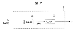
図7に示す遅延同期ループ1は、前記実施形態1で説明した図15、図16、図17に記載の遅延同期ループを適用することができる。図17に記載のエッジコンバイナ遅延同期ループを本実施形態に適用する場合は、帰還信号(Fb)を制御回路2に出力することで適用することが可能である。
As the delay locked loop 1 shown in FIG. 7, the delay locked loop described in FIGS. 15, 16, and 17 described in the first embodiment can be applied. When the edge combiner delay locked loop shown in FIG. 17 is applied to the present embodiment, it can be applied by outputting the feedback signal (Fb) to the
図9に、図7に示す制御回路2の一構成例を示す。
FIG. 9 shows a configuration example of the
図9に示す制御回路2は、排他的論理和回路(EXOR)2aとカウンタ(COUNT)23を具備して成り、排他的論理和回路2aは、基準信号(Fr)と出力信号(Fo)が入力して、排他的論理和信号(EXO)をカウンタ23に出力して、カウンタ23は、排他的論理和信号(EXO)の立ち下がりエッジをあらかじめ設定されたカウント数だけ基準信号(Fr)をカウントして、所定のカウント数になるまでは制御信号(S)としてローを出力して、所定のカウント数に到達したら制御信号(S)としてハイを出力する。
The
図10に、図9に示す制御回路2を適用した図7に示す遅延同期回路の動作例を示す。図10に示す動作例では、制御回路2は排他的論理和信号(EXO)の立ち下がりエッジを3回カウントして制御信号(S)の極性を変えるときの動作例である。
FIG. 10 shows an operation example of the delay synchronization circuit shown in FIG. 7 to which the
基準信号(Fr)と出力信号(Fo)は図10に示すような波形であるとする。この両信号が排他的論理和回路(EXOR)2aに入力すると、図10に示すような排他的論理和信号(EXO)を出力する。 It is assumed that the reference signal (Fr) and the output signal (Fo) have waveforms as shown in FIG. When these two signals are input to the exclusive OR circuit (EXOR) 2a, an exclusive OR signal (EXO) as shown in FIG. 10 is output.
カウンタ23は初期状態として制御信号(S)としてローを出力するように設定されており、基準信号(Fr)の立ち下がりエッジを検出してカウント数を数えて、カウント数が3になるまでは制御信号(S)としてローを出力して、カウント数が3になったら、制御信号(S)としてハイを出力する。カウンタ23は、制御信号(S)として一度ハイを出力する動作に入ったら、同じ状態を保持する。
The
遅延同期ループ1のループ外に、上述したような動作を行う制御回路2を持つことで、定常位相誤差を生じることなく、遅延同期ループのハーモニックロックを回避することが可能となる。
By having the
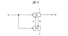
(実施形態3)
図8に、本発明の実施形態3に係る遅延同期回路の構成例を示す。本実施形態3は前記実施形態2の変形例である。
(Embodiment 3)
FIG. 8 shows a configuration example of the delay synchronization circuit according to the third embodiment of the present invention. The third embodiment is a modification of the second embodiment.
本実施形態3に係る遅延同期回路は、例えば、遅延同期ループ(DL)1と制御回路(CNT)2などから構成される。 The delay locked loop according to the third embodiment includes, for example, a delay locked loop (DL) 1 and a control circuit (CNT) 2.
遅延同期ループ(DL)1は、基準信号(Fr)と制御信号(S)が入力して帰還信号(Fb)と出力信号(Fo)を出力する。制御回路2は基準信号(Fr)と帰還信号(Fb)が入力して制御信号(S)を出力する。
The delay locked loop (DL) 1 receives the reference signal (Fr) and the control signal (S) and outputs a feedback signal (Fb) and an output signal (Fo). The
図17に、図8に記載の遅延同期ループ1の構成例を示す。 FIG. 17 shows a configuration example of the delay locked loop 1 shown in FIG.
図17に示す遅延同期ループ1は、位相周波数比較器(PFD)11、チャージポンプ(CP)12、ループフィルタ(LF)13、電圧制御遅延線(VCDL)14、プリチャージ(PC)15、エッジコンバイナ(EC)16から構成される。 17 includes a phase frequency comparator (PFD) 11, a charge pump (CP) 12, a loop filter (LF) 13, a voltage control delay line (VCDL) 14, a precharge (PC) 15, an edge. It is composed of a combiner (EC) 16.
位相周波数比較器11は、基準信号(Fr)と帰還信号(Fb)と制御信号(S)が入力して、基準信号(Fr)と帰還信号(Fb)の比較信号をチャージポンプ12に出力する。チャージポンプ12は、比較信号に応じたパルス信号をループフィルタ13に出力する。ループフィルタ13は、パルス信号をアナログ信号に変換して電圧制御遅延線14に出力する。電圧制御遅延線14は、基準信号とアナログ信号が入力して、アナログ信号で制御された遅延時間だけ基準信号の位相を遅延した各位相の信号を出力する。
The
図17では4種類の位相の信号を出力している。基準信号に対して最も位相が遅延された信号を帰還信号(Fb)として位相周波数比較器11に入力している。一方、電圧制御遅延線14の各位相の出力信号は、エッジコンバイナ16(EC)に入力する。エッジコンバイナは、位相の異なる各信号を足し合わせて基準信号(Fr)の定数倍の周波数を持つ出力信号(Fo)を生成する。
In FIG. 17, four types of phase signals are output. A signal whose phase is delayed most with respect to the reference signal is input to the
図8に示す制御回路2は、前述の図9に示す制御回路を適用することが可能である。本実施形態3の動作詳細は、前記実施形態1及び実施形態2と同様であるため省略する。
The
本実施形態3により、前記実施形態1及び実施形態2と同様の効果を得ることができる。 According to the third embodiment, the same effects as those of the first and second embodiments can be obtained.
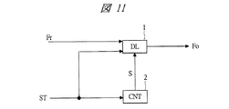
(実施形態4)
図11に、本発明の実施形態4に係る遅延同期回路の構成を示す。
(Embodiment 4)
FIG. 11 shows a configuration of a delay synchronization circuit according to the fourth embodiment of the present invention.
本実施形態4に係る遅延同期回路は、例えば、遅延同期ループ(DL)1と制御回路(CNT)2などから構成される。 The delay locked loop circuit according to the fourth embodiment includes, for example, a delay locked loop (DL) 1 and a control circuit (CNT) 2.
遅延同期ループ(DL)1は、基準信号(Fr)と制御信号(S)とスタンバイ信号(ST)が入力して出力信号(Fo)を出力する。制御回路2は、基準信号(Fr)と帰還信号(Fb)とスタンバイ信号(ST)が入力して制御信号(S)を出力する。
The delay locked loop (DL) 1 receives the reference signal (Fr), the control signal (S), and the standby signal (ST) and outputs an output signal (Fo). The
スタンバイ信号(ST)は、遅延同期ループ1の動作状態を規定する信号で、例えば、スタンバイ信号(ST)がハイのときに遅延同期ループ1は通常動作を行い、ローのときにスタンバイ動作になるとする。 The standby signal (ST) is a signal that defines an operation state of the delay locked loop 1. For example, when the standby signal (ST) is high, the delay locked loop 1 performs a normal operation, and when the standby signal (ST) is low, the standby signal (ST) is in a standby operation. To do.
図12に、図11に示す制御回路2の構成例を示す。また、図14に、図12に示す遅延回路21の構成を示す。
FIG. 12 shows a configuration example of the
図12に示す制御回路2は、遅延回路(DELAY)21とトリミング部(TRIM)22を具備して成り、スタンバイ信号(ST)とトリミング信号(T)が入力している遅延回路21は、トリミング信号(T)で設定された遅延時間だけスタンバイ信号(ST)を遅延した信号を制御信号(S)として出力する。
The
図13に、図12に示す制御回路2を用いた、図11に示す遅延同期回路の動作例を示す。
FIG. 13 shows an operation example of the delay synchronization circuit shown in FIG. 11 using the
スタンバイ信号(ST)がローのとき、基準信号(Fr)はクロック信号ではなく、一定信号になる。スタンバイ信号(ST)がハイになると基準信号がクロック信号となり遅延同期ループ1に入力される。また、スタンバイ信号(ST)は制御回路2にも入力されて、制御回路において、スタンバイ信号(ST)の立ち上がりエッジが、基準信号(Fr)の最初の立ち下がりエッジと2番目の立ち上がりエッジの間に来るように遅延させて、制御信号(S)として遅延同期ループに出力する。この遅延時間がトリミング信号(T)で制御される。制御信号(S)を入力された遅延同期ループ1は、図13に示すように正常動作をすることが可能となる。
When the standby signal (ST) is low, the reference signal (Fr) is not a clock signal but a constant signal. When the standby signal (ST) becomes high, the reference signal becomes a clock signal and is input to the delay locked loop 1. The standby signal (ST) is also input to the
(実施形態5)
本発明の実施形態5に係る半導体集積回路装置は、前記実施形態1〜4に係る遅延同期回路を半導体集積回路装置に適用したものである。
(Embodiment 5)
A semiconductor integrated circuit device according to Embodiment 5 of the present invention is obtained by applying the delay synchronization circuit according to Embodiments 1 to 4 to a semiconductor integrated circuit device.
図25に、本発明の実施形態5に係る半導体集積回路装置(LSI)の構成を示す。 FIG. 25 shows the configuration of a semiconductor integrated circuit device (LSI) according to Embodiment 5 of the present invention.
本実施形態5に係る半導体集積回路装置(LSI)6は、例えば、論理回路(LOGIC)61と遅延同期回路(DLL)10などから構成される。 The semiconductor integrated circuit device (LSI) 6 according to the fifth embodiment includes, for example, a logic circuit (LOGIC) 61 and a delay synchronization circuit (DLL) 10.
半導体集積回路装置6に外付けされた発振子5から基準信号(Fr)が遅延同期回路10に入力される。遅延同期回路10は、前記実施形態1〜5に記載の遅延同期回路であり、基準信号(Fr)に同期した出力信号(Fo)を生成し、論理回路61に出力する。論理回路61はデータ演算処理を行う回路であり、遅延同期回路10により生成された出力信号(Fo)を動作クロックにして動作する。
A reference signal (Fr) is input to the
本発明の前提として検討した図20、図21に記載の遅延同期回路を用いると、遅延同期回路で発生した定常位相誤差は出力信号(Fo)にとってジッタとなり論理回路61の動作マージンを狭めてしまう。
20 and 21 studied as the premise of the present invention, the stationary phase error generated in the delay synchronization circuit becomes jitter for the output signal (Fo) and narrows the operation margin of the
また、近年の半導体集積回路装置の高速化によって論理回路61の動作速度を決定する遅延同期回路の出力信号(Fo)が高速化するに従い当該遅延同期回路で発生した定常位相誤差が論理回路61の動作不良を起こす原因ともなる。
Further, as the output signal (Fo) of the delay synchronization circuit that determines the operation speed of the
さらに、当該遅延同期回路に、エッジコンバイナ型遅延同期回路を用いて基準信号(Fr)の逓倍周波数を持つ出力信号(Fo)を生成して論理回路61を高速動作させる半導体集積回路装置においては、当該遅延同回路の定常位相誤差が原因で出力信号(Fo)が所望の周波数にならず、論理回路61が動作できないという不具合が発生するおそれがある。
Further, in the semiconductor integrated circuit device that generates an output signal (Fo) having a frequency multiplied by the reference signal (Fr) by using an edge combiner type delay synchronization circuit in the delay synchronization circuit and operates the
そこで、図25に示すように、前記実施の形態1〜4による遅延同期回路10を用いることで、定常位相誤差を発生することなく出力信号(Fo)を生成できることから、論理回路61の動作不良を起こすことなく半導体集積回路装置6を正常動作させることができるようになる。
Therefore, as shown in FIG. 25, since the output signal (Fo) can be generated without generating a steady phase error by using the
次に、本実施の形態5に係る半導体集積回路装置の応用例として、前記実施の形態1〜4に係る遅延同期回路を、送受信装置とシステムオンチップに適用した例を説明する。 Next, as an application example of the semiconductor integrated circuit device according to the fifth embodiment, an example in which the delay synchronization circuit according to the first to fourth embodiments is applied to a transmission / reception device and a system-on-chip will be described.
図26に、前記実施の形態1〜4に係る遅延同期回路を用いたUSBトランシーバの構成を示す。 FIG. 26 shows a configuration of a USB transceiver using the delay synchronization circuit according to the first to fourth embodiments.
本実施の形態5に係る半導体集積回路装置(LSI)6は、例えば、USBトランシーバの物理層(PHY)であり、アナログフロントエンド(AFE)31と、エンコーダ(ENC)32と、デシリアライザ(DES)33と、クロックデータリカバリ(CDR)34,35と、マルチプレクサ(MUX)36と、デコーダ(DEC)37と、シリアライザ(SER)38などから成る論理回路(LOGIC)61と、遅延同期回路(DLL)10などを具備してなり、リンク層(LINK)4から出力された送信信号(TX)は当該デシリアライザ33によってパラレル信号からシリアル信号に変換されてエンコーダ32によって信号処理を行い、アナログフロントエンド31を介してUSBケーブルから出力される。出力の際に、USBトランシーバのモードによってハイスピードモード(HS)、フルスピードモード(FS)の2系統の経路が選択される。一方、USBケーブルから受信した信号はアナログフロントエンド31を介してハイスピードモード(HS)ならクロックデータリカバリ34、フルスピードモード(FS)ならクロックデータリカバリ35にデータが出力される。各クロックデータリカバリ34,35は発振子5の出力信号(Fr)を受けて信号を生成する遅延同期回路(DLL)10の出力信号をクロックとして受けてデータとクロックを同期させ、マルチプレクサ36に信号を出力する。マルチプレクサ36はデコーダ37に選択した信号を出力し、デコーダ37は信号処理をしてシリアライザ38に信号を出力する。シリアライザ38はシリアルデータをパラレルデータに変換してリンク層4に出力する。
The semiconductor integrated circuit device (LSI) 6 according to the fifth embodiment is, for example, a physical layer (PHY) of a USB transceiver, an analog front end (AFE) 31, an encoder (ENC) 32, and a deserializer (DES). 33, a clock data recovery (CDR) 34, 35, a multiplexer (MUX) 36, a decoder (DEC) 37, a logic circuit (LOGIC) 61 including a serializer (SER) 38, etc., and a delay synchronization circuit (DLL) The transmission signal (TX) output from the link layer (LINK) 4 is converted from a parallel signal to a serial signal by the
この半導体集積回路装置(USB物理層)6において、クロックデータリカバリのクロックを生成する遅延同期回路は、前記実施形態1〜4に記載の遅延同期回路が最適である。 In this semiconductor integrated circuit device (USB physical layer) 6, the delay synchronization circuit described in the first to fourth embodiments is optimal as a delay synchronization circuit that generates a clock for clock data recovery.
図27に、前記実施の形態1〜4に係る遅延同期回路を用いたDVDドライブ用LSIの構成を示す。 FIG. 27 shows the configuration of a DVD drive LSI using the delay synchronization circuit according to the first to fourth embodiments.
本実施の形態5に係る半導体集積回路装置(LSI)6は、例えば、DVDドライブ用LSIとされ、記録再生部の論理回路(LOGIC)61と、送受信部(ATAPI)62とを具備して成り、ホスト(HOST)9から出力された送信信号(TX)は送受信部62を介して論理回路61内の論理回路611に入力される。論理回路611によって信号処理された送信信号はピックアップ(Pick−up)8を介してメディア7に書込まれる。ここで、論理回路611は遅延同期回路10が生成するクロックを動作クロックとして動作する。この遅延同期回路10は発振子5の出力信号(Fr)を入力して所望の信号を生成する動作を行い、前記実施形態1〜4に記載の遅延同期回路が好適である。
The semiconductor integrated circuit device (LSI) 6 according to the fifth embodiment is, for example, a DVD drive LSI, and includes a logic circuit (LOGIC) 61 of a recording / playback unit and a transmission / reception unit (ATAPI) 62. The transmission signal (TX) output from the host (HOST) 9 is input to the
以上、本発明者によってなされた発明をその実施の形態に基づき具体的に説明したが、本発明は前記実施の形態に限定されるものではなく、その要旨を逸脱しない範囲で種々変更可能であることはいうまでもない。 As mentioned above, the invention made by the present inventor has been specifically described based on the embodiment. However, the invention is not limited to the embodiment, and various modifications can be made without departing from the scope of the invention. Needless to say.
上記各実施形態によれば、(1)遅延同期ループの誤動作を回避することができる、(2)基準信号(Fr)が、位相比較器と遅延線に同じタイミングで入力される、または(3)定常位相誤差が発生しないで所望の出力信号を得ることができる、という効果を奏することとなる。 According to each of the above embodiments, (1) malfunction of the delay locked loop can be avoided, (2) the reference signal (Fr) is input to the phase comparator and the delay line at the same timing, or (3 ) It is possible to obtain a desired output signal without generating a steady phase error.
また、本発明の上記各実施形態は、半導体装置、電子機器等の製造業に適用して有効である。 Each of the above embodiments of the present invention is effective when applied to the manufacturing industry of semiconductor devices, electronic devices, and the like.
1 遅延同期ループ(DL)
2,3 制御回路(CNT)
2a 排他的論理和回路(EXOR)
4 リンク層(LINK)
5 発振子
6 半導体集積回路装置(LSI)
7 メディア
8 ピックアップ(Pick−up)
9 ホスト(HOST)
10 遅延同期回路(DLL)
11 位相周波数比較器(PFD)
11a,11f,11g,111,112,113,114,115,116,117,118,119,244 NANDゲート
11b,11c,11d,11e,212,213,214,215,216,217,218,242,246 インバータ
12 チャージポンプ(CP)
13 ループフィルタ(LF)
14 電圧制御遅延線(VCDL)
15 プリチャージ(PC)
16 エッジコンバイナ(EC)
21 遅延回路(DELAY)
22 トリミング部(TRIM)
23 カウンタ(COUNT)
24 パルス発生器(SHOT)
31 アナログフロントエンド(AFE)
32 エンコーダ(ENC)
33 デシリアライザ(DES)
34,35 クロックデータリカバリ(CDR)
36 マルチプレクサ(MUX)
37 デコーダ(DEC)
38 シリアライザ(SER)
61,611,613 論理回路(LOGIC)
62 送受信部(ATAPI)
241,243 NORゲート
245 Dフリップフロップ(DFF)
247 スタンバイシーケンス回路(SEQ)
1 Delay locked loop (DL)
2,3 Control circuit (CNT)
2a Exclusive OR circuit (EXOR)
4 Link layer (LINK)
5
7
9 Host (HOST)
10 Delay synchronization circuit (DLL)
11 Phase frequency comparator (PFD)
11a, 11f, 11g, 111, 112, 113, 114, 115, 116, 117, 118, 119, 244
13 Loop filter (LF)
14 Voltage Control Delay Line (VCDL)
15 Precharge (PC)
16 Edge combiner (EC)
21 Delay circuit (DELAY)
22 Trimming part (TRIM)
23 Counter (COUNT)
24 Pulse generator (SHOT)
31 Analog Front End (AFE)
32 Encoder (ENC)
33 Deserializer (DES)
34, 35 Clock data recovery (CDR)
36 Multiplexer (MUX)
37 Decoder (DEC)
38 Serializer (SER)
61,611,613 Logic circuit (LOGIC)
62 Transmitter / Receiver (ATAPI)
241,243 NOR gate 245 D flip-flop (DFF)
247 Standby sequence circuit (SEQ)
Claims (10)
前記遅延同期ループの動作を制御する制御信号を出力する制御回路とを具備して成り、
前記遅延同期ループは、基準信号と前記制御信号とが入力して出力信号を出力し、
前記制御回路は、基準信号と前記出力信号とが入力して前記制御信号を出力し、
前記制御回路は、排他的論理和回路とカウンタとを含み、
前記排他的論理和回路は、前記基準信号と前記出力信号とが入力し、前記排他的論理和回路の出力が前記カウンタに入力され、
前記カウンタにより前記排他的論理和回路の出力をカウントし、前記カウンタのカウント数が設定値に到達するまでは前記制御信号として前記遅延同期ループが動作しない設定信号を出力し、前記カウンタのカウント数が前記設定値に到達した後、前記制御信号として前記遅延同期ループが動作する設定信号を出力することを特徴とする遅延同期回路。 A delay-locked loop;
A control circuit that outputs a control signal for controlling the operation of the delay locked loop,
The delay locked loop receives a reference signal and the control signal and outputs an output signal,
The control circuit receives a reference signal and the output signal and outputs the control signal,
The control circuit includes an exclusive OR circuit and a counter,
The exclusive OR circuit receives the reference signal and the output signal, and outputs the exclusive OR circuit to the counter.
The counter counts the output of the exclusive OR circuit, and outputs a setting signal that does not operate the delay locked loop as the control signal until the counter count reaches a set value. After reaching the set value, the delay locked loop circuit outputs a set signal for operating the delay locked loop as the control signal.
前記遅延同期ループの動作を制御する制御信号を出力する制御回路とを具備して成り、
前記遅延同期ループは、基準信号と前記制御信号とが入力して出力信号を出力し、
前記制御回路は、基準信号が入力して前記制御信号を出力し、
前記遅延同期ループは、さらに、帰還信号を出力し、前記帰還信号が前記制御回路に入力され、
前記制御回路は、排他的論理和回路とカウンタとを含み、
前記排他的論理和回路は、前記基準信号と前記帰還信号とが入力し、前記排他的論理和回路の出力が前記カウンタに入力され、
前記カウンタにより前記排他的論理和回路の出力をカウントし、前記カウンタのカウント数が設定値に到達するまでは前記制御信号として前記遅延同期ループが動作しない設定信号を出力し、前記カウンタのカウント数が前記設定値に到達した後、前記制御信号として前記遅延同期ループが動作する設定信号を出力することを特徴とする遅延同期回路。 A delay-locked loop;
A control circuit that outputs a control signal for controlling the operation of the delay locked loop,
The delay locked loop receives a reference signal and the control signal and outputs an output signal,
Wherein the control circuit outputs the control signal to the reference signal is input,
The delay locked loop further outputs a feedback signal, and the feedback signal is input to the control circuit,
The control circuit includes an exclusive OR circuit and a counter,
The exclusive OR circuit receives the reference signal and the feedback signal, and the output of the exclusive OR circuit is input to the counter.
The counter counts the output of the exclusive OR circuit, and outputs a setting signal that does not operate the delay locked loop as the control signal until the counter count reaches a set value. After reaching the set value, the delay locked loop circuit outputs a set signal for operating the delay locked loop as the control signal.
前記遅延同期ループは、位相比較器を具備して成り、
前記基準信号と前記出力信号と前記制御信号とが、前記位相比較器に入力し、
前記位相比較器は、前記制御信号を用い、前記基準信号と前記出力信号との位相を比較することを特徴とする遅延同期回路。 In claim 1,
The delay locked loop comprises a phase comparator,
The reference signal, the output signal, and the control signal are input to the phase comparator,
The phase comparator uses the control signal to compare phases of the reference signal and the output signal.
前記遅延同期ループは、位相比較器を具備して成り、
前記基準信号と前記出力信号と前記制御信号とが、前記位相比較器に入力し、
前記位相比較器は、前記制御信号を用い、前記基準信号と前記出力信号との位相を比較することを特徴とする遅延同期回路。 In claim 2,
The delay locked loop comprises a phase comparator,
The reference signal, the output signal, and the control signal are input to the phase comparator,
The phase comparator uses the control signal to compare phases of the reference signal and the output signal.
前記遅延同期ループは、さらに、スタンバイ信号が入力し、
前記制御回路は、さらに、前記スタンバイ信号が入力する回路であることを特徴とする遅延同期回路。 In claim 1 ,
The delay locked loop further receives a standby signal,
The delay synchronization circuit according to claim 1, wherein the control circuit is a circuit to which the standby signal is input.
前記遅延同期ループは、位相比較器を具備して成り、
前記基準信号と前記出力信号と前記制御信号とが、前記位相比較器に入力し、
前記位相比較器は、前記制御信号により、前記基準信号と前記出力信号との位相を比較する回路であることを特徴とする遅延同期回路。 In claim 1 ,
The delay locked loop comprises a phase comparator,
The reference signal, the output signal, and the control signal are input to the phase comparator,
The phase comparator is a circuit for comparing phases of the reference signal and the output signal according to the control signal.
前記遅延同期ループは、さらに、スタンバイ信号が入力し、
前記制御回路は、さらに、前記スタンバイ信号が入力する回路であることを特徴とする遅延同期回路。 In claim 6 ,
The delay locked loop further receives a standby signal,
The delay synchronization circuit according to claim 1, wherein the control circuit is a circuit to which the standby signal is input.
前記遅延同期ループは、さらに、スタンバイ信号が入力し、
前記制御回路は、さらに、前記スタンバイ信号が入力する回路であることを特徴とする遅延同期回路。 In claim 2 ,
The delay locked loop further receives a standby signal,
The delay synchronization circuit according to claim 1, wherein the control circuit is a circuit to which the standby signal is input.
前記遅延同期ループは、位相比較器を具備して成り、
前記基準信号と前記出力信号と前記制御信号とが、前記位相比較器に入力し、
前記位相比較器は、前記制御信号により、前記基準信号と前記出力信号との位相を比較する回路であることを特徴とする遅延同期回路。 In claim 2 ,
The delay locked loop comprises a phase comparator,
The reference signal, the output signal, and the control signal are input to the phase comparator,
The phase comparator is a circuit for comparing phases of the reference signal and the output signal according to the control signal.
前記遅延同期ループは、さらに、スタンバイ信号が入力し、
前記制御回路は、さらに、前記スタンバイ信号が入力する回路であることを特徴とする遅延同期回路。 In claim 9 ,
The delay locked loop further receives a standby signal,
The delay synchronization circuit according to claim 1, wherein the control circuit is a circuit to which the standby signal is input.
Priority Applications (7)
| Application Number | Priority Date | Filing Date | Title |
|---|---|---|---|
| JP2006067243A JP5134779B2 (en) | 2006-03-13 | 2006-03-13 | Delay synchronization circuit |
| TW095145171A TWI399038B (en) | 2006-03-13 | 2006-12-05 | Delay synchronous circuit and semiconductor integrated circuit device |
| CN2006101566680A CN101039108B (en) | 2006-03-13 | 2006-12-30 | Delay locked loop circuit and semiconductor integrated circuit device |
| US11/648,652 US7482850B2 (en) | 2006-03-13 | 2007-01-03 | Delay locked loop circuit and semiconductor integrated circuit device |
| KR1020070002478A KR20070093322A (en) | 2006-03-13 | 2007-01-09 | Delay locked loop circuit and semiconductor integrated circuit device |
| EP07000456.9A EP1835623B1 (en) | 2006-03-13 | 2007-01-10 | Delay locked loop circuit and semiconductor integrated circuit device |
| US12/354,391 US7675334B2 (en) | 2006-03-13 | 2009-01-15 | Delay locked loop circuit and semiconductor integrated circuit device |
Applications Claiming Priority (1)
| Application Number | Priority Date | Filing Date | Title |
|---|---|---|---|
| JP2006067243A JP5134779B2 (en) | 2006-03-13 | 2006-03-13 | Delay synchronization circuit |
Publications (3)
| Publication Number | Publication Date |
|---|---|
| JP2007243877A JP2007243877A (en) | 2007-09-20 |
| JP2007243877A5 JP2007243877A5 (en) | 2009-03-12 |
| JP5134779B2 true JP5134779B2 (en) | 2013-01-30 |
Family
ID=38050939
Family Applications (1)
| Application Number | Title | Priority Date | Filing Date |
|---|---|---|---|
| JP2006067243A Expired - Fee Related JP5134779B2 (en) | 2006-03-13 | 2006-03-13 | Delay synchronization circuit |
Country Status (6)
| Country | Link |
|---|---|
| US (2) | US7482850B2 (en) |
| EP (1) | EP1835623B1 (en) |
| JP (1) | JP5134779B2 (en) |
| KR (1) | KR20070093322A (en) |
| CN (1) | CN101039108B (en) |
| TW (1) | TWI399038B (en) |
Families Citing this family (19)
| Publication number | Priority date | Publication date | Assignee | Title |
|---|---|---|---|---|
| WO2009090448A2 (en) * | 2008-01-15 | 2009-07-23 | Atmel Corporation | Proportional phase comparator and method for phase-aligning digital signals |
| JP2009278528A (en) * | 2008-05-16 | 2009-11-26 | Elpida Memory Inc | Dll circuit, and semiconductor device |
| KR100996175B1 (en) * | 2008-12-26 | 2010-11-24 | 주식회사 하이닉스반도체 | Semiconductor device |
| KR101012678B1 (en) * | 2009-02-04 | 2011-02-09 | 연세대학교 산학협력단 | Delay locked loop and electirc device including the same |
| TWI474184B (en) * | 2009-06-08 | 2015-02-21 | Via Tech Inc | Universal serial bus device and universal serial bus system |
| JP5588254B2 (en) | 2009-08-04 | 2014-09-10 | キヤノン株式会社 | Delay locked loop circuit |
| TWI396386B (en) * | 2010-05-06 | 2013-05-11 | Princeton Technology Corp | One-shot circuit integrated into chip, transmitter capable of reducing start-up time and method thereof |
| US8248124B2 (en) * | 2010-06-03 | 2012-08-21 | Intel Corporation | Methods and apparatuses for delay-locked loops and phase-locked loops |
| KR102053352B1 (en) * | 2013-02-25 | 2019-12-09 | 삼성전자주식회사 | Phase locked loop for preventing harmonic lock and devices having the same |
| KR101657339B1 (en) * | 2013-05-22 | 2016-09-19 | 매그나칩 반도체 유한회사 | DLL Operation mode controller circuit and method for controlling thereof |
| US9584105B1 (en) * | 2016-03-10 | 2017-02-28 | Analog Devices, Inc. | Timing generator for generating high resolution pulses having arbitrary widths |
| JP6390683B2 (en) * | 2016-09-28 | 2018-09-19 | ミツミ電機株式会社 | Semiconductor integrated circuit |
| WO2018208990A1 (en) * | 2017-05-09 | 2018-11-15 | The Regents Of The University Of California | Systems and methods for low-power near-field-communication |
| WO2019036519A1 (en) | 2017-08-14 | 2019-02-21 | The Regents Of The University Of California | Load-induced resonance-shift-keying modulation scheme for simultaneous near-field wireless power and data transmission through a pair of inductive coils |
| US11527992B2 (en) | 2019-09-19 | 2022-12-13 | Analog Devices International Unlimited Company | Rotary traveling wave oscillators with distributed stubs |
| CN113179099B (en) * | 2020-09-18 | 2022-04-01 | 上海司南卫星导航技术股份有限公司 | Phase-locked loop circuit, control method thereof, semiconductor device and electronic equipment |
| US11539353B2 (en) * | 2021-02-02 | 2022-12-27 | Analog Devices International Unlimited Company | RTWO-based frequency multiplier |
| US11290114B1 (en) | 2021-06-01 | 2022-03-29 | SambaNova Systems, Inc. | Variable-length clock stretcher with passive mode jitter reduction |
| CN113381753B (en) * | 2021-06-08 | 2022-07-12 | 天津大学 | Start-up circuit for delay locked loop |
Family Cites Families (20)
| Publication number | Priority date | Publication date | Assignee | Title |
|---|---|---|---|---|
| JPS6098727A (en) * | 1983-11-04 | 1985-06-01 | Mitsubishi Electric Corp | Out of synchronism detecting circuit |
| JPS62247624A (en) * | 1986-04-07 | 1987-10-28 | Mitsubishi Electric Corp | Phased locked loop circuit |
| JPS63136825A (en) * | 1986-11-28 | 1988-06-09 | Mitsubishi Electric Corp | Phase locked loop with synchronous/asynchronous state detecting counter |
| JP3275222B2 (en) * | 1994-03-04 | 2002-04-15 | 富士通株式会社 | Phase locked oscillator |
| JP3481148B2 (en) * | 1998-10-15 | 2003-12-22 | 富士通株式会社 | Integrated circuit device having DLL circuit |
| JPH11205102A (en) * | 1998-01-13 | 1999-07-30 | Mitsubishi Electric Corp | Delay synchronization circuit |
| US6239634B1 (en) * | 1999-05-19 | 2001-05-29 | Parthus Technologies | Apparatus and method for ensuring the correct start-up and locking of a delay locked loop |
| JP3808670B2 (en) | 1999-08-19 | 2006-08-16 | 富士通株式会社 | Semiconductor integrated circuit |
| JP2002064371A (en) | 2000-08-14 | 2002-02-28 | Nec Corp | Phase frequency comparator and initializing method for the same |
| US6504408B1 (en) * | 2001-07-09 | 2003-01-07 | Broadcom Corporation | Method and apparatus to ensure DLL locking at minimum delay |
| US6628154B2 (en) * | 2001-07-31 | 2003-09-30 | Cypress Semiconductor Corp. | Digitally controlled analog delay locked loop (DLL) |
| US6683478B2 (en) | 2001-11-13 | 2004-01-27 | Samsung Electronics Co., Ltd. | Apparatus for ensuring correct start-up and phase locking of delay locked loop |
| TW558872B (en) * | 2002-05-21 | 2003-10-21 | Via Tech Inc | Delay-locked loop device and method for generating clock signal |
| US7477716B2 (en) | 2003-06-25 | 2009-01-13 | Mosaid Technologies, Inc. | Start up circuit for delay locked loop |
| US6867627B1 (en) * | 2003-09-16 | 2005-03-15 | Integrated Device Technology, Inc. | Delay-locked loop (DLL) integrated circuits having high bandwidth and reliable locking characteristics |
| US7002384B1 (en) * | 2004-01-16 | 2006-02-21 | Altera Corporation | Loop circuitry with low-pass noise filter |
| KR100605588B1 (en) | 2004-03-05 | 2006-07-28 | 주식회사 하이닉스반도체 | Delay locked loop in semicinductor memory device and its clock locking method |
| JP3993860B2 (en) * | 2004-04-19 | 2007-10-17 | 富士通株式会社 | DLL circuit |
| KR100537202B1 (en) * | 2004-05-06 | 2005-12-16 | 주식회사 하이닉스반도체 | Semiconductor device capable of using lock-in state information of delay locked loop |
| US7355464B2 (en) * | 2005-05-09 | 2008-04-08 | Micron Technology, Inc. | Apparatus and method for controlling a delay- or phase-locked loop as a function of loop frequency |
-
2006
- 2006-03-13 JP JP2006067243A patent/JP5134779B2/en not_active Expired - Fee Related
- 2006-12-05 TW TW095145171A patent/TWI399038B/en not_active IP Right Cessation
- 2006-12-30 CN CN2006101566680A patent/CN101039108B/en not_active Expired - Fee Related
-
2007
- 2007-01-03 US US11/648,652 patent/US7482850B2/en not_active Expired - Fee Related
- 2007-01-09 KR KR1020070002478A patent/KR20070093322A/en not_active Application Discontinuation
- 2007-01-10 EP EP07000456.9A patent/EP1835623B1/en active Active
-
2009
- 2009-01-15 US US12/354,391 patent/US7675334B2/en active Active
Also Published As
| Publication number | Publication date |
|---|---|
| US7675334B2 (en) | 2010-03-09 |
| EP1835623A1 (en) | 2007-09-19 |
| US20090134924A1 (en) | 2009-05-28 |
| EP1835623B1 (en) | 2013-08-14 |
| CN101039108B (en) | 2010-09-08 |
| US20070210842A1 (en) | 2007-09-13 |
| JP2007243877A (en) | 2007-09-20 |
| KR20070093322A (en) | 2007-09-18 |
| TW200737726A (en) | 2007-10-01 |
| US7482850B2 (en) | 2009-01-27 |
| CN101039108A (en) | 2007-09-19 |
| TWI399038B (en) | 2013-06-11 |
Similar Documents
| Publication | Publication Date | Title |
|---|---|---|
| JP5134779B2 (en) | Delay synchronization circuit | |
| US8542044B2 (en) | Semiconductor integrated circuit and method for driving the same | |
| JP5149076B2 (en) | Delay locked loop | |
| US7368966B2 (en) | Clock generator and clock duty cycle correction method | |
| JP4868353B2 (en) | Delay locked loop | |
| US7633324B2 (en) | Data output strobe signal generating circuit and semiconductor memory apparatus having the same | |
| US6593786B2 (en) | Register controlled DLL reducing current consumption | |
| US7605623B2 (en) | Semiconductor memory apparatus with a delay locked loop circuit | |
| TW201007424A (en) | Apparatus and method for multi-phase clock generation | |
| TWI417879B (en) | Delay locked loop circuit of semiconductor device | |
| US8144530B2 (en) | Semiconductor memory device and method for generating output enable signal | |
| US8164370B2 (en) | Clock control circuit and semiconductor device including the same | |
| US8482331B2 (en) | Open loop type delay locked loop and method for operating the same | |
| JP2008219866A (en) | Semiconductor memory device and method of driving same | |
| JP2004325410A (en) | Input and output circuit | |
| US8638137B2 (en) | Delay locked loop | |
| JP4583088B2 (en) | Strobe signal delay device and semiconductor device including the same | |
| KR20210029400A (en) | Delay line, delay locked loop circuit and semiconductor apparatus using the same | |
| TWI407437B (en) | Semiconductor memory device and method for driving the semiconductor memory device | |
| KR100911191B1 (en) | Apparatus for Adjusting Frequency and DLL Circuit with the Same | |
| KR100685613B1 (en) | Delay locked loop for high speed | |
| Jaiswal et al. | Adaptive Low-Power Synchronization Technique for Multiple Source-Synchronous Clocks in High-Speed Communication Systems | |
| KR20210029402A (en) | Delay line, delay locked loop circuit and semiconductor apparatus using the same | |
| KR20090121469A (en) | Semiconductor memory device |
Legal Events
| Date | Code | Title | Description |
|---|---|---|---|
| A621 | Written request for application examination |
Free format text: JAPANESE INTERMEDIATE CODE: A621 Effective date: 20081002 |
|
| A521 | Request for written amendment filed |
Free format text: JAPANESE INTERMEDIATE CODE: A523 Effective date: 20090122 |
|
| A711 | Notification of change in applicant |
Free format text: JAPANESE INTERMEDIATE CODE: A712 Effective date: 20100528 |
|
| A977 | Report on retrieval |
Free format text: JAPANESE INTERMEDIATE CODE: A971007 Effective date: 20100617 |
|
| A131 | Notification of reasons for refusal |
Free format text: JAPANESE INTERMEDIATE CODE: A131 Effective date: 20100706 |
|
| A521 | Request for written amendment filed |
Free format text: JAPANESE INTERMEDIATE CODE: A523 Effective date: 20100903 |
|
| A02 | Decision of refusal |
Free format text: JAPANESE INTERMEDIATE CODE: A02 Effective date: 20110222 |
|
| A521 | Request for written amendment filed |
Free format text: JAPANESE INTERMEDIATE CODE: A523 Effective date: 20120919 |
|
| A01 | Written decision to grant a patent or to grant a registration (utility model) |
Free format text: JAPANESE INTERMEDIATE CODE: A01 |
|
| A61 | First payment of annual fees (during grant procedure) |
Free format text: JAPANESE INTERMEDIATE CODE: A61 Effective date: 20121112 |
|
| FPAY | Renewal fee payment (event date is renewal date of database) |
Free format text: PAYMENT UNTIL: 20151116 Year of fee payment: 3 |
|
| R150 | Certificate of patent or registration of utility model |
Free format text: JAPANESE INTERMEDIATE CODE: R150 |
|
| S531 | Written request for registration of change of domicile |
Free format text: JAPANESE INTERMEDIATE CODE: R313531 |
|
| R350 | Written notification of registration of transfer |
Free format text: JAPANESE INTERMEDIATE CODE: R350 |
|
| LAPS | Cancellation because of no payment of annual fees |