JP5130896B2 - Semiconductor device drive circuit - Google Patents
Semiconductor device drive circuit Download PDFInfo
- Publication number
- JP5130896B2 JP5130896B2 JP2007324500A JP2007324500A JP5130896B2 JP 5130896 B2 JP5130896 B2 JP 5130896B2 JP 2007324500 A JP2007324500 A JP 2007324500A JP 2007324500 A JP2007324500 A JP 2007324500A JP 5130896 B2 JP5130896 B2 JP 5130896B2
- Authority
- JP
- Japan
- Prior art keywords
- mos transistor
- resistor
- gate
- drive circuit
- output
- Prior art date
- Legal status (The legal status is an assumption and is not a legal conclusion. Google has not performed a legal analysis and makes no representation as to the accuracy of the status listed.)
- Expired - Fee Related
Links
Images


Description
本発明は、半導体素子の駆動回路に関する。 The present invention relates to a drive circuit for a semiconductor element.
半導体素子をスイッチング動作させる駆動回路として、例えば、図5に示す駆動回路41が用いられる。
図5において、IC12は、駆動信号のオン期間、オフ期間を可変する信号を生成し、生成した信号をpチャネルMOSトランジスタQ1とnチャネルMOSトランジスタQ2のゲートに出力する。pチャネルMOSトランジスタQ1のドレインは、pチャネルMOSトランジスタQ3のゲートと抵抗R41の一端に接続されている。pチャネルMOSトランジスタQ1のソースには電源電圧VDが供給される。
For example, a
In FIG. 5, the
nチャネルMOSトランジスタQ2のドレインは、nチャネルMOSトランジスタQ4のゲートと抵抗R41の他端に接続され、ソースは接地されている。
pチャネルMOSトランジスタQ3とnチャネルMOSトランジスタQ4は縦続接続され、pチャネルMOSトランジスタQ3のソースは抵抗R42を介して電源電圧VDに接続されている。そして、MOSトランジスタQ3とQ4の接続点の電圧が、図示しない制御対象のMOSトランジスタのゲートに出力されている。MOSトランジスタQ4のソースは抵抗R43を介して接地されている。
The drain of n-channel MOS transistor Q2 is connected to the gate of n-channel MOS transistor Q4 and the other end of resistor R41, and the source is grounded.
p-channel MOS transistor Q3 and the n-channel MOS transistor Q4 is connected in cascade, the source of the p-channel MOS transistor Q3 is connected to the power supply voltage V D through a resistor R42. The voltage at the connection point between the MOS transistors Q3 and Q4 is output to the gate of the MOS transistor to be controlled (not shown). The source of the MOS transistor Q4 is grounded through a resistor R43.
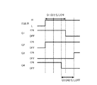
図6は、IC12とMOSトランジスタQ1〜Q4の動作波形を示す図である。
IC12の出力がローレベルからハイレベルに変化すると、MOSトランジスタQ1がオフ、MOSトランジスタQ2がオンに変化する。IC12の出力がローレベルのとき、MOSトランジスタQ3のゲートには電源電圧VDが印加されているので、MOSトランジスタQ1がオフ状態に変化しても、MOSトランジスタQ3のゲート電圧が正の一定値に上昇するまでの間、MOSトランジスタQ3はオフ状態を維持する。
FIG. 6 is a diagram showing operation waveforms of the
When the output of the
他方、MOSトランジスタQ4のゲートにはそれまで電源電圧VDが印加されていたので、MOSトランジスタQ2がオンとなっても、MOSトランジスタQ4のゲート電圧はすぐには所定電圧以下とならず、一定時間経過した後オフ状態となる。 On the other hand, since the power supply voltage V D has been applied to the gate of the MOS transistor Q4, the gate voltage of the MOS transistor Q4 does not immediately fall below the predetermined voltage even if the MOS transistor Q2 is turned on. It turns off after a lapse of time.
そのため、図6に示すようにMOSトランジスタQ3とQ4の両方がオンとなる期間が生じる。駆動回路41の出力電流を大きくするため、抵抗R42、R43は小さな値に設計されるので、MOSトランジスタQ3、Q4が同時にオンすると大きな貫通電流が流れしまう。
Therefore, there is a period in which both MOS transistors Q3 and Q4 are turned on as shown in FIG. Since the resistors R42 and R43 are designed to have a small value in order to increase the output current of the
また、電源起動時に電源電圧VDが一定値に達するまでの期間は、IC12の出力はローレベルであることが望ましいが、実際には、IC12が正常に動作する電圧に達するまでの間、IC12の出力は不定であり、IC12の電源端子に印加される電圧がハイレベルの信号としてそのまま出力されてしまうことがある。その結果、電源の起動時に、駆動回路11から半導体素子をオンにする信号が出力される可能性があった。
In addition, it is desirable that the output of the
特許文献1には、第2のスイッチング素子のオン動作に従属して電源電圧が得られる従属的電源回路に接続したインバータにおいて、従属的電源回路の電圧が所定値以上に上昇するまで、第1のスイッチング素子のオン動作を禁止する回路を設けることが記載されている。
本発明の課題は、駆動回路の電源電圧が所定値以上に上昇するまで駆動回路がオン動作しないこと、半導体素子をスイッチング動作させる駆動回路の出力段のトランジスタに貫通電流が流れないようにすることである。 An object of the present invention is to prevent the drive circuit from turning on until the power supply voltage of the drive circuit rises to a predetermined value or more, and to prevent a through current from flowing through the transistor in the output stage of the drive circuit that performs switching operation of the semiconductor element It is.
本発明は、半導体素子をスイッチング動作させる駆動信号を生成する駆動回路であって、駆動信号のオン期間及びオフ期間を決める信号を生成するICの出力がゲートに印加される第1のトランジスタと、前記第1のトランジスタと縦続接続され、前記ICの出力がツェナーダイオードを介してゲートに印加される第2のトランジスタとからなり、前記第1及び第2のトランジスタはMOSトランジスタからなり、前記第1のMOSトランジスタのドレインまたはソースにゲートが接続された第3のMOSトランジスタと、前記第2のMOSトランジスタのドレインまたはソースに一端が接続され、他端が電源電圧に接続された第2の抵抗と、前記第2の抵抗の一端に、ゲートが接続された第4のMOSトランジスタとを有する。 The present invention is a driving circuit for generating a drive signal for the semiconductor element is a switching operation, a first transistor output IC for generating a signal for determining the ON period and OFF period of the driving signal is applied to the gate , connected in cascade with said first transistor, consists of a second transistor an output of the IC is applied via a Zener diode to the gate, the first and second transistors comprises a MOS transistor, wherein a third MOS transistor having a gate connected to the drain or source of the first MOS transistor, one end to the drain or the source of the second MOS transistor is connected, a second connected other end to the power supply voltage a resistor, the second one end of the resistor, and a fourth MOS transistor having a gate connected.
この駆動回路によれば、駆動回路の電源電圧が所定値以上に上昇するまで駆動回路がオン動作しないようにできる。
また、このように構成することで、駆動回路の電源電圧が所定値以上に上昇するまで駆動回路がオン動作しないようにできる。
上記の駆動回路において、前記第1と第2のMOSトランジスタは第1の抵抗を介して縦続接続され、前記第3のMOSトランジスタのソースは第3の抵抗の一端に接続され、ドレインは前記第4のMOSトランジスタのドレインに接続され、前記第3の抵抗の他端は前記電源電圧に接続され、前記第4のMOSトランジスタのソースは第4の抵抗を介して接地され、前記第1の抵抗の値は、前記第3の抵抗及び前記第4の抵抗の値に比べて大きな値である。
According to this drive circuit, the drive circuit can be prevented from being turned on until the power supply voltage of the drive circuit rises to a predetermined value or more.
Further, with this configuration, the drive circuit can be prevented from being turned on until the power supply voltage of the drive circuit rises to a predetermined value or more.
In the driving circuit, the first and second MOS transistors are connected in cascade via a first resistor, the source of the third MOS transistor is connected to one end of a third resistor, and the drain is connected to the first resistor. The other end of the third resistor is connected to the power supply voltage, the source of the fourth MOS transistor is grounded via a fourth resistor, and the first resistor is connected to the drain of the fourth MOS transistor. The value of is larger than the values of the third resistor and the fourth resistor.
このように構成することで、第1の抵抗の値は、第3の抵抗、第4の抵抗の値に比べて大きな値にすることができ、第1のMOSトランジスタ、第2のMOSトランジスタに流れる貫通電流は動作上問題が無い値にできる。
上記の駆動回路において、前記第1のMOSトランジスタのゲートには、第1のダイオードと第1のツェナーダイオードが直列に接続され、前記第2のMOSトランジスタのゲートには、第2のダイオードと第2のツェナーダイオードが直列に接続されている。
With this configuration, the value of the first resistor can be made larger than the values of the third resistor and the fourth resistor, and the first MOS transistor and the second MOS transistor The flowing through current can be set to a value that causes no problem in operation.
In the above driving circuit, wherein the gate of the first MOS transistor, a first diode and the first zener diode is connected in series, the gate of said second MOS transistor, a second diode And a second Zener diode are connected in series.
このように構成することで、駆動回路の電源電圧が所定値以上に上昇するまで駆動回路がオン動作しないようにできると共に、駆動回路の出力段のトランジスタが同時にオンするのを防止できる。 With this configuration, the drive circuit can be prevented from being turned on until the power supply voltage of the drive circuit rises to a predetermined value or more, and the transistors in the output stage of the drive circuit can be prevented from being turned on at the same time.
本発明によれば、駆動回路の電源電圧が所定値以上に上昇するまで駆動回路がオン動作せず、かつ駆動回路の出力段のトランジスタが同時にオンするのを防止できる。 According to the present invention, it is possible to prevent the drive circuit from being turned on until the power supply voltage of the drive circuit rises to a predetermined value or more, and to prevent the transistors in the output stage of the drive circuit from being turned on simultaneously.
以下、本発明の好適な実施の形態について説明する。図1は、第1の実施の形態の駆動回路11の回路図である。この第1の実施の形態は、駆動回路11の電源電圧が所定値以上に上昇するまで駆動回路11をオン動作させないためのものである。 Hereinafter, preferred embodiments of the present invention will be described. FIG. 1 is a circuit diagram of the drive circuit 11 according to the first embodiment. In the first embodiment, the drive circuit 11 is not turned on until the power supply voltage of the drive circuit 11 rises to a predetermined value or more.
駆動回路11は、半導体素子、例えばMOSトランジスタQ5をスイッチング動作させるための駆動信号を生成する回路である。IC12は、信号生成用の専用の半導体集積回路であり、駆動信号のオン期間及びオフ期間を決める信号を出力する。IC12の出力は、pチャネルMOSトランジスタQ1のゲートとツェナーダイオードZD2のカソードに印加されている。ツェナーダイオードZD2のアノードは、nチャネルMOSトランジスタQ2のゲートと、抵抗R5の一端に接続されており、抵抗R5の他端は接地(または共通電位、以下、接地として説明する)されている。
The drive circuit 11 is a circuit that generates a drive signal for switching the semiconductor element, for example, the MOS transistor Q5. The
MOSトランジスタQ1のソースは電源電圧VDに接続され、ドレインはpチャネルMOSトランジスタQ3のゲートと、抵抗R1の一端に接続されている。MOSトランジスタQ2のドレインは、抵抗R1の他端と、nチャネルMOSトランジスタQ4のゲートに接続されている。MOSトランジスタQ4のゲートには抵抗R6が接続され、その抵抗R6の他端は電源電圧VDに接続されている。 The source of the MOS transistor Q1 is connected to power supply voltage V D, the drain is connected to the gate of the p-channel MOS transistors Q3, one end of the resistor R1. The drain of the MOS transistor Q2 is connected to the other end of the resistor R1 and the gate of the n-channel MOS transistor Q4. The gate of the MOS transistor Q4 resistor R6 is connected, the other end of the resistor R6 is connected to the power supply voltage V D.
MOSトランジスタQ3のソースは抵抗R2の一端に接続され、ドレインはnチャネルMOSトランジスタQ4のドレインに接続されている。抵抗R2の他端は電源電圧VDに接続されている。nチャネルMOSトランジスタQ4のソースは抵抗R3を介して接地されている。 The source of the MOS transistor Q3 is connected to one end of the resistor R2, and the drain is connected to the drain of the n-channel MOS transistor Q4. The other end of the resistor R2 is connected to the power supply voltage V D. The source of the n-channel MOS transistor Q4 is grounded via a resistor R3.
MOSトランジスタQ3とMOSトランジスタQ4の接続点は、制御対象のnチャネルMOSトランジスタQ5のゲートと接続されており、MOSトランジスタQ3、Q4の出力電圧が駆動信号としてMOSトランジスタQ5のゲートに出力されている。MOSトランジスタQ5のゲートには抵抗R4が接続され、抵抗R4の他端は接地されている。 The connection point between the MOS transistor Q3 and the MOS transistor Q4 is connected to the gate of the n-channel MOS transistor Q5 to be controlled, and the output voltages of the MOS transistors Q3 and Q4 are output as drive signals to the gate of the MOS transistor Q5. . A resistor R4 is connected to the gate of the MOS transistor Q5, and the other end of the resistor R4 is grounded.
図1の駆動回路11は、IC12の出力がローレベルのとき、pチャネルMOSトランジスタQ1がオン、nチャネルMOSトランジスタQ2がオフ状態になる。
MOSトランジスタQ1がオン状態のとき、pチャネルMOSトランジスタQ3のゲートには電源電圧VDが印加されるので、MOSトランジスタQ3はオフ状態となる。MOSトランジスタQ2がオフ状態のとき、nチャネルMOSトランジスタQ4のゲートには、抵抗R6を介して電源電圧VDのが印加されるので、MOSトランジスタQ4はオン状態となる。
In the drive circuit 11 of FIG. 1, when the output of the
When MOS transistor Q1 is in the ON state, the power supply voltage V D to the gate of the p-channel MOS transistor Q3 is applied, the MOS transistor Q3 is turned off. When MOS transistor Q2 is off, the gate of the n-channel MOS transistor Q4, since the power supply voltage V D is applied via a resistor R6, the MOS transistor Q4 is turned on.
IC12の出力がローレベルからハイレベルに変化する過程で、出力電圧、つまりMOSトランジスタQ1のゲート電圧が一定電圧(MOSトランジスタQ1がオフとなる電圧)以上になると、MOSトランジスタQ1はオフ状態に変化する。このとき、IC12の出力電圧が、ツェナーダイオードZD2のツェナー電圧未満であれば、MOSトランジスタQ2はオフ状態を維持する。
When the output of the
すなわち、IC12の出力電圧がツェナーダイオードZD2のツェナー電圧未満のとき、MOSトランジスタQ2はオフ状態になる。
MOSトランジスタQ2がオフのとき、pチャネルMOSトランジスタQ3のゲートには、抵抗R6、R1を介して電源電圧VDが印加されるので、pチャネルMOSトランジスタQ3はオフ状態を維持する。
That is, when the output voltage of the
When MOS transistor Q2 is off, the gate of the p-channel MOS transistor Q3, the power supply voltage V D through a resistor R6, R1 is applied, the p-channel MOS transistor Q3 is kept off.
他方、MOSトランジスタQ4のゲートには抵抗R6を介して電源電圧VDが印加されるので、MOSトランジスタQ4はオン状態を維持する。これによりMOSトランジスタQ5をオフ状態にすることができる。 On the other hand, the power supply voltage V D through a resistor R6 to the gate of the MOS transistor Q4 is applied, the MOS transistor Q4 is maintained in an ON state. Thereby, MOS transistor Q5 can be turned off.
すなわち、駆動回路11の電源電圧VDが低く、IC12の出力電圧がツェナーダイオードZD2のツェナー電圧未満のときには、MOSトランジスタQ2をオフ状態、MOSトランジスタQ4をオン状態にできるので、駆動回路11から半導体素子をオン状態にする信号が出力されるのを防止することができる。
That is, when the power supply voltage V D of the drive circuit 11 is low and the output voltage of the
上述した第1の実施の形態によれば、IC12の出力とMOSトランジスタQ2のゲートとの間にツェナーダイオードZD2を挿入し、MOSトランジスタQ4のゲートに抵抗R6を介して電源電圧VDを印加することで、駆動回路11の電源電圧VDが所定値以上となるまで、駆動回路11からMOSトランジスタQ5をオン状態にする信号が出力されないようにできる。
According to the first embodiment described above, the Zener diode ZD2 is inserted between the output of the
なお、図1の回路において、MOSトランジスタQ2がオン状態(またはオフ状態)になる電圧を制限するための回路はツェナーダイオードを用いたものに限らず、他の構成の電圧制限回路を用いても良い。 In the circuit of FIG. 1, the circuit for limiting the voltage at which the MOS transistor Q2 is turned on (or off) is not limited to the one using a zener diode, and a voltage limiting circuit having another configuration may be used. good.
次に、図2は、第2の実施の形態の駆動回路21の回路図である。この第2の実施の形態は、電源の起動時の駆動回路21の誤動作を防止するものであると共に、スイッチング時に駆動回路21の出力段のトランジスタが同時にオンするのを防止するものである。以下、図1と同じ要素には同じ符号を付けてそれらの説明は省略する。 Next, FIG. 2 is a circuit diagram of the drive circuit 21 according to the second embodiment. In the second embodiment, the malfunction of the drive circuit 21 at the time of starting the power supply is prevented, and the transistors in the output stage of the drive circuit 21 are prevented from being simultaneously turned on at the time of switching. In the following, the same elements as those in FIG.
図2において、pチャネルMOSトランジスタQ1のゲートは抵抗R21を介して電源電圧VDに接続され、さらにツェナーダイオードZD1とダイオードD1を介してIC12の出力に接続されている。ダイオードD1のカソードがIC12の出力に接続され、ツェナーダイオードZD1のカソードがゲートに接続されている。
2, the gate of the p-channel MOS transistor Q1 is connected to power supply voltage V D through a resistor R21, and is further connected to the output of IC12 via a Zener diode ZD1 and the diode D1. The cathode of the diode D1 is connected to the output of the
nチャネルMOSトランジスタQ2のゲートは、ツェナーダイオードZD2とダイオードD2を介してIC12の出力に接続され、さらに抵抗R5を介して接地されている。ダイオードD2のアノードがIC12の出力に接続され、ツェナーダイオードZD2のアノードがゲートに接続されている。
The gate of the n-channel MOS transistor Q2 is connected to the output of the
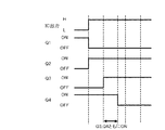
上記の駆動回路21の動作を、図3の波形図を参照して説明する。IC12の出力がローレベルのときは、pチャネルMOSトランジスタQ1のゲートには、ツェナーダイオードZD1のツェナー電圧とダイオードD1の順方向電圧を加算した電圧が印加され、MOSトランジスタQ1はオン状態になっている。
The operation of the drive circuit 21 will be described with reference to the waveform diagram of FIG. When the output of the
他方、MOSトランジスタQ2のゲートに印加される電圧は、IC12の出力がローレベルであることからほぼ0Vとなり、MOSトランジスタQ2はオフ状態になっている。
IC12の出力電圧がローレベルからハイレベルに変化し、その出力電圧がツェナーダイオードZD2のツェナー電圧以上となると、MOSトランジスタQ2はオン状態になる。
On the other hand, the voltage applied to the gate of the MOS transistor Q2 is almost 0 V because the output of the
When the output voltage of the
一方、IC12の出力がハイレベルになっても、ダイオードD1によりIC12からMOSトランジスタQ1のゲートには電流は流入せず、電源電圧VDから抵抗R21の経路で電流が流れるので、ゲート電圧が一定値(オフ電圧)に達するまでの一定時間MOSトランジスタQ1はオン状態を維持する。
On the other hand, even if the output of the
すなわち、図3に示すように、MOSトランジスタQ2は、IC12の出力がハイレベルに変化したとき直ぐにオン状態に変化するが、MOSトランジスタQ1はゲート電圧が一定値に達するまでの一定時間オン状態を維持する。従って、その間、MOSトランジスタQ1とQ2は同時にオン状態となる(図3のQ1、Q2がともにオンの期間)。MOSトランジスタQ1とQ2が同時にオン状態となることで、MOSトランジスタQ1とQ2に貫通電流が流れるが、抵抗R1の値は、出力段の抵抗R2、R3の値に比べて大きな値に設計することができるので、トランジスタQ1、Q2に流れる貫通電流は動作上問題が無い値にできる。
That is, as shown in FIG. 3, the MOS transistor Q2 is turned on immediately when the output of the
MOSトランジスタQ1がオン状態のとき、MOSトランジスタQ3のゲートには電源電圧VDが印加されるので、MOSトランジスタQ3はその間オフ状態を維持する。
MOSトランジスタQ2がオン状態に変化しても、MOSトランジスタQ4のゲート電圧が一定値以下になるまでMOSトランジスタQ4はオン状態を維持する(図3のQ4がオン状態の期間)。
When MOS transistor Q1 is in the ON state, the power supply voltage V D to the gate of the MOS transistor Q3 is applied, the MOS transistor Q3 is kept between the off state.
Even if the MOS transistor Q2 changes to the ON state, the MOS transistor Q4 maintains the ON state until the gate voltage of the MOS transistor Q4 becomes a certain value or less (period in which Q4 in FIG. 3 is ON).
すなわち、図3の駆動回路21は、IC12の出力がローレベルからハイレベルに変化してから一定期間、MOSトランジスタQ1とQ2を同時にオン状態とすることで、その間MOSトランジスタQ3をオフ状態にすることができる。これにより、MOSトランジスタQ3とQ4が同時にオンして貫通電流が流れるのを防止できる。
That is, the drive circuit 21 in FIG. 3 simultaneously turns on the MOS transistors Q1 and Q2 for a certain period after the output of the
一定時間が経過してMOSトランジスタQ4のゲートの電荷が放出されてゲート電圧が一定値未満となると、MOSトランジスタQ4がオフ状態に変化する(図3のQ4がオフに変化するタイミング)。その後、MOSトランジスタQ1のゲート電圧が一定値以上となり、MOSトランジスタQ1がオフ状態に変化すると(図3のQ1がオフに変化するタイミング)、MOSトランジスタQ3のゲート電圧が次第に減少し、一定時間後にMOSトランジスタQ3がオン状態に変化する(図3のQ3がオンに変化するタイミング)。このとき、MOSトランジスタQ3とQ4の接続点の出力電圧Voutは正の電圧となり、半導体素子をオンさせる駆動信号が出力される。 When a certain time passes and the gate charge of the MOS transistor Q4 is released and the gate voltage becomes less than a certain value, the MOS transistor Q4 changes to an off state (timing when Q4 in FIG. 3 changes to off). After that, when the gate voltage of the MOS transistor Q1 becomes a certain value or more and the MOS transistor Q1 changes to an off state (timing when Q1 in FIG. 3 changes to off), the gate voltage of the MOS transistor Q3 gradually decreases, and after a certain time The MOS transistor Q3 changes to the ON state (timing when Q3 in FIG. 3 changes to ON). At this time, the output voltage Vout at the connection point between the MOS transistors Q3 and Q4 becomes a positive voltage, and a drive signal for turning on the semiconductor element is output.
次に、電源起動時の動作を説明する。電源の立ち上がり時にIC12が誤動作してハイレベルの信号(例えば、その時の電源電圧VDとほぼ等しい電圧値の信号)が出力されても、IC12の出力電圧が、ツェナーダイオードZD2のツェナー電圧(ダイオードD2の順方向電圧を含む)未満のときには、MOSトランジスタQ2はオフ状態を維持する。
Next, the operation at the time of power activation will be described. Even if the
MOSトランジスタQ2がオフ状態のとき、MOSトランジスタQ4のゲートには、抵抗R6を介して電源電圧VDが印加されるので、MOSトランジスタQ4はオン状態となる。 When MOS transistor Q2 is off, the gate of the MOS transistor Q4, since the power supply voltage V D via the resistor R6 is applied, the MOS transistor Q4 is turned on.
従って、駆動回路21の出力電圧Voutは接地電位となり、半導体素子(例えば、nチャネルMOSトランジスタQ5)をオフ状態に保つことができる。これにより、電源起動時にIC12の誤動作によりハイレベルの信号が出力される場合でも、駆動回路21の出力電圧Voutを接地電位にして、制御対象の半導体素子をオフ状態にすることができる。
Therefore, the output voltage Vout of the drive circuit 21 becomes the ground potential, and the semiconductor element (for example, the n-channel MOS transistor Q5) can be kept in the off state. As a result, even when a high level signal is output due to a malfunction of the
上述した第2の実施の形態によれば、IC12の出力が変化したときに、駆動回路21の出力段のMOSトランジスタQ3、Q4が同時にオンするのを防止できる。さらに、電源起動時にIC12が誤動作して外部の半導体素子をオンにする信号(例えば、ハイレベルの信号)が出力されても、ツェナーダイオードZD2によりゲート電圧を制限することで、駆動回路21から半導体素子をオン状態にする信号が出力されるのを防止することができる。
According to the second embodiment described above, it is possible to prevent the MOS transistors Q3 and Q4 in the output stage of the drive circuit 21 from being turned on simultaneously when the output of the
次に、図4は、第3の実施の形態の駆動回路31の回路図である。この第3の実施の形態は、駆動回路31をバイポーラトランジスタQ1、Q2で構成した例であり、トランジスタQ1、Q2が駆動回路31の出力段のトランジスタに該当する。
Next, FIG. 4 is a circuit diagram of the
IC12の出力は、ツェナーダイオードZD3と抵抗R11を介して、トランジスタQ1のベースに入力している。また、IC12の出力は、抵抗R12を介してトランジスタQ2のベースに入力している。トランジスタQ1のコレクタは抵抗R13を介して電源電圧VDに接続され、トランジスタQ1のエミッタとトランジスタQ2のエミッタが接続され、トランジスタQ2のコレクタは接地(または基準電位)されている。トランジスタQ1とトランジスタQ2の接続点から、図示しない半導体素子を駆動する駆動電圧Voutが出力される。
The output of the
IC12の出力がローレベルのとき、トランジスタQ1がオフ、トランジスタQ2がオンとなっている。IC12の出力がローレベルからハイレベルに変化すると、トランジスタQ2はオフ状態に変化するが、トランジスタQ1は、IC12の出力電圧が、ツェナーダイオードZD3のツェナー電圧以上で、かつトランジスタQ1のオン電圧以上となるまでオフ状態を維持する。これにより、IC12の出力が変化するときに、駆動回路31の出力段のトランジスタQ1、Q2が同時にオンするのを防止できる。
When the output of the
本発明は上述した実施の形態に限らず、例えば、以下のように構成しても良い。
駆動回路に使用するトランジスタはMOSトランジスタに限らず、バイポーラトランジスタ等の他の半導体素子でも良い。また、駆動回路は、縦続接続されたトランジスタが2段接続された回路に限らず、図4に示すような1段構成の回路、あるいは3段以上の回路であっても良い。
The present invention is not limited to the embodiment described above, and may be configured as follows, for example.
The transistor used in the drive circuit is not limited to a MOS transistor, and may be another semiconductor element such as a bipolar transistor. Further, the drive circuit is not limited to a circuit in which two cascade-connected transistors are connected, but may be a circuit having a single-stage configuration as shown in FIG. 4 or a circuit having three or more stages.
11、21、31、41 駆動回路
12 IC
ZD1、ZD2、ZD3 ツェナーダイオード
Q1〜Q5 トランジスタ
11, 21, 31, 41
ZD1, ZD2, ZD3 Zener diodes Q1-Q5 transistors
Claims (2)
駆動信号のオン期間及びオフ期間を決める信号を生成するICの出力がゲートに印加される第1のトランジスタと、
前記第1のトランジスタと縦続接続され、前記ICの出力がツェナーダイオードを介してゲートに印加される第2のトランジスタとからなり、
前記第1及び第2のトランジスタはMOSトランジスタからなり、
前記第1のMOSトランジスタのドレインまたはソースにゲートが接続された第3のMOSトランジスタと、
前記第2のMOSトランジスタのドレインまたはソースに一端が接続され、他端が電源電圧に接続された第2の抵抗と、
前記第2の抵抗の一端に、ゲートが接続された第4のMOSトランジスタとを有し、
前記第1と第2のMOSトランジスタは第1の抵抗を介して縦続接続され、
前記第3のMOSトランジスタのソースは第3の抵抗の一端に接続され、ドレインは前記第4のMOSトランジスタのドレインに接続され、
前記第3の抵抗の他端は前記電源電圧に接続され、
前記第4のMOSトランジスタのソースは第4の抵抗を介して接地され、
前記第1の抵抗の値は、前記第3の抵抗及び前記第4の抵抗の値に比べて大きな値である半導体素子の駆動回路。 A drive circuit for generating a drive signal for switching a semiconductor element,
A first transistor output IC for generating a signal for determining the ON period and OFF period of the driving signal is applied to the gate,
The cascade connected to the first transistor consists of a second transistor an output of the IC is applied to the gate via a Zener diode,
The first and second transistors are MOS transistors,
A third MOS transistor having a gate connected to the drain or source of the first MOS transistor;
One end to the drain or the source of the second MOS transistor is connected, and a second resistor connected other end to the power supply voltage,
To one end of said second resistor, it possesses a fourth MOS transistor having a gate connected,
The first and second MOS transistors are cascaded through a first resistor,
The source of the third MOS transistor is connected to one end of a third resistor, the drain is connected to the drain of the fourth MOS transistor,
The other end of the third resistor is connected to the power supply voltage,
The source of the fourth MOS transistor is grounded via a fourth resistor;
A drive circuit for a semiconductor element , wherein a value of the first resistor is larger than values of the third resistor and the fourth resistor .
前記第2のMOSトランジスタのゲートには、第2のダイオードと第2のツェナーダイオードが直列に接続されている請求項1記載の半導体素子の駆動回路。 Wherein the gate of the first MOS transistor, a first diode and the first zener diode is connected in series,
Wherein the gate of the second MOS transistor, the second diode and drive circuit in accordance with claim 1, wherein the second zener diode are connected in series.
Priority Applications (1)
| Application Number | Priority Date | Filing Date | Title |
|---|---|---|---|
| JP2007324500A JP5130896B2 (en) | 2007-12-17 | 2007-12-17 | Semiconductor device drive circuit |
Applications Claiming Priority (1)
| Application Number | Priority Date | Filing Date | Title |
|---|---|---|---|
| JP2007324500A JP5130896B2 (en) | 2007-12-17 | 2007-12-17 | Semiconductor device drive circuit |
Publications (3)
| Publication Number | Publication Date |
|---|---|
| JP2009147784A JP2009147784A (en) | 2009-07-02 |
| JP2009147784A5 JP2009147784A5 (en) | 2011-02-03 |
| JP5130896B2 true JP5130896B2 (en) | 2013-01-30 |
Family
ID=40917849
Family Applications (1)
| Application Number | Title | Priority Date | Filing Date |
|---|---|---|---|
| JP2007324500A Expired - Fee Related JP5130896B2 (en) | 2007-12-17 | 2007-12-17 | Semiconductor device drive circuit |
Country Status (1)
| Country | Link |
|---|---|
| JP (1) | JP5130896B2 (en) |
Families Citing this family (2)
| Publication number | Priority date | Publication date | Assignee | Title |
|---|---|---|---|---|
| JP2015208111A (en) * | 2014-04-21 | 2015-11-19 | ニチコン株式会社 | gate drive circuit |
| CN108512403B (en) * | 2018-04-10 | 2020-02-14 | 峰岹科技(深圳)有限公司 | MOS tube driving circuit, driving chip and motor |
Family Cites Families (3)
| Publication number | Priority date | Publication date | Assignee | Title |
|---|---|---|---|---|
| JPH01305618A (en) * | 1988-06-02 | 1989-12-08 | Mitsubishi Electric Corp | Cmos inverter output circuit |
| JP2731049B2 (en) * | 1991-06-24 | 1998-03-25 | 三菱電機株式会社 | CMOS output circuit |
| JP4727360B2 (en) * | 2005-09-20 | 2011-07-20 | 東芝三菱電機産業システム株式会社 | Gate circuit of insulated gate semiconductor device |
-
2007
- 2007-12-17 JP JP2007324500A patent/JP5130896B2/en not_active Expired - Fee Related
Also Published As
| Publication number | Publication date |
|---|---|
| JP2009147784A (en) | 2009-07-02 |
Similar Documents
| Publication | Publication Date | Title |
|---|---|---|
| JP3678208B2 (en) | Load driving semiconductor device | |
| JP5315026B2 (en) | Semiconductor device | |
| JP4830507B2 (en) | Bootstrap circuit | |
| US20090153122A1 (en) | Dropper-type regulator | |
| JP5254678B2 (en) | Level shift circuit and power semiconductor device | |
| JP2008147755A (en) | Driving circuit and semiconductor device using the same | |
| JP2012070333A (en) | Level shift circuit and switching regulator using the same | |
| US9444249B2 (en) | Semiconductor driving device and semiconductor device | |
| US9024660B2 (en) | Driving circuit with zero current shutdown and a driving method thereof | |
| KR100963310B1 (en) | Control circuit for dc/dc converter | |
| JP2010004093A (en) | Output driving circuit | |
| JP2008258939A (en) | Multichannel semiconductor integrated circuit | |
| KR101603566B1 (en) | Semiconductor device drive circuit and semiconductor device drive unit | |
| US6903590B2 (en) | Pulse generating circuit and high-side driver circuit | |
| US20050110556A1 (en) | Bootstrap driver | |
| JP6259782B2 (en) | Level shift circuit | |
| US6084446A (en) | Power on reset circuit | |
| JP2010028522A (en) | Semiconductor device | |
| US20090167419A1 (en) | Voltage converting circuit | |
| JP5130896B2 (en) | Semiconductor device drive circuit | |
| JP2024014878A (en) | semiconductor equipment | |
| JP4066231B2 (en) | Switching regulator | |
| JP4705264B2 (en) | Switching regulator | |
| US20220173586A1 (en) | Semiconductor device | |
| US10734995B1 (en) | Output circuit |
Legal Events
| Date | Code | Title | Description |
|---|---|---|---|
| A521 | Written amendment |
Free format text: JAPANESE INTERMEDIATE CODE: A523 Effective date: 20101215 |
|
| A621 | Written request for application examination |
Free format text: JAPANESE INTERMEDIATE CODE: A621 Effective date: 20101215 |
|
| A977 | Report on retrieval |
Free format text: JAPANESE INTERMEDIATE CODE: A971007 Effective date: 20120717 |
|
| A131 | Notification of reasons for refusal |
Free format text: JAPANESE INTERMEDIATE CODE: A131 Effective date: 20120724 |
|
| A521 | Written amendment |
Free format text: JAPANESE INTERMEDIATE CODE: A523 Effective date: 20120912 |
|
| TRDD | Decision of grant or rejection written | ||
| A01 | Written decision to grant a patent or to grant a registration (utility model) |
Free format text: JAPANESE INTERMEDIATE CODE: A01 Effective date: 20121009 |
|
| A01 | Written decision to grant a patent or to grant a registration (utility model) |
Free format text: JAPANESE INTERMEDIATE CODE: A01 |
|
| A61 | First payment of annual fees (during grant procedure) |
Free format text: JAPANESE INTERMEDIATE CODE: A61 Effective date: 20121022 |
|
| FPAY | Renewal fee payment (event date is renewal date of database) |
Free format text: PAYMENT UNTIL: 20151116 Year of fee payment: 3 |
|
| FPAY | Renewal fee payment (event date is renewal date of database) |
Free format text: PAYMENT UNTIL: 20151116 Year of fee payment: 3 |
|
| LAPS | Cancellation because of no payment of annual fees |