JP5125357B2 - Manufacturing method of electro-optical device - Google Patents
Manufacturing method of electro-optical device Download PDFInfo
- Publication number
- JP5125357B2 JP5125357B2 JP2007250783A JP2007250783A JP5125357B2 JP 5125357 B2 JP5125357 B2 JP 5125357B2 JP 2007250783 A JP2007250783 A JP 2007250783A JP 2007250783 A JP2007250783 A JP 2007250783A JP 5125357 B2 JP5125357 B2 JP 5125357B2
- Authority
- JP
- Japan
- Prior art keywords
- light
- layer
- substrate
- liquid crystal
- electro
- Prior art date
- Legal status (The legal status is an assumption and is not a legal conclusion. Google has not performed a legal analysis and makes no representation as to the accuracy of the status listed.)
- Expired - Fee Related
Links
Images


Landscapes
- Liquid Crystal (AREA)
- Projection Apparatus (AREA)
Description
本発明は、液晶装置などの電気光学装置の製造方法、当該方法で製造した電気光学装置、および当該電気光学装置を備えた投射型表示装置に関するものである。 The present invention relates to a method for manufacturing an electro-optical device such as a liquid crystal device, an electro-optical device manufactured by the method, and a projection display device including the electro-optical device.
電気光学装置では、配線領域の確保や混色防止を目的に縦横に延在する格子状の遮光領域を設け、この遮光領域で囲まれた画素開口領域から変調光を出射する。例えば、代表的な電気光学装置である液晶装置は、図12(a)に示すように、画素電極が形成された素子基板10と、この素子基板10に対向配置された対向基板20と、素子基板10と対向基板20との間に保持された液晶層50とを備えており、素子基板10において配線および画素スイッチング用のトランジスタが形成された領域14、および対向基板20においてブラックマトリクスやブラックストライプと称せられる遮光層24が形成された領域によって、遮光領域100cが規定され、遮光領域100cの内側は、画素電極を備えた画素開口領域100dになっている。このように構成した液晶装置は、素子基板10の側から入射した光を液晶層50によって光変調した後、対向基板20から出射する構成、あるいは、対向基板20の側から入射した光を液晶層50によって光変調した後、素子基板10から出射する構成になっているため、入射光を効率よく利用するには、入射光を画素開口領域100dに効率よく導く必要がある。
In the electro-optical device, a grid-like light shielding region extending vertically and horizontally is provided for the purpose of securing a wiring region and preventing color mixing, and modulated light is emitted from a pixel opening region surrounded by the light shielding region. For example, as shown in FIG. 12A, a liquid crystal device, which is a typical electro-optical device, includes an
そこで、対向基板20の側から入射した光を液晶層50によって光変調した後、素子基板10から出射する構造の液晶装置においては、ドライエッチングやレーザエッチングなどにより、図12(a)、(b)に示すように、対向基板20側において遮光領域100cと重なる領域に、入射光を画素開口領域100dに導く反射性の斜面265を備えた断面V字形状の偏向溝264(図12(b)において右下がりの斜線を付した領域)を縦横に形成した偏向用基板20eを用いることが提案されている(特許文献1参照)。
しかしながら、図12(a)、(b)に示すような偏向溝264を形成するにあたって、特許文献1に記載の方法を採用すると、生産性が極めて低いとともに、偏向溝264の斜面265の角度などにばらつきが発生しやすいという問題点がある。すなわち、特許文献1に記載の方法では、図13(a)に示すように、偏向溝264を形成するためのエッチング対象領域に対応する開孔部61を備えたレジストマスク60を偏向用基板20eに形成した後、偏向用基板20eの基板面およびレジストマスク60にドライエッチングを行い、図13(b)に示すように、断面V字形状の偏向溝264を形成する。次に、偏向用基板20eより屈折率が低い樹脂材料や空気などの低屈折率材料263を偏向溝264に充填した状態で、偏向用基板20eの基板面に接着剤20xを介してカバー基板20yを貼り付け、カバー基板20yの表面に遮光層24および共通電極21を順に形成し、対向基板20を得る。
However, when the
ここで、偏向溝264はかなりの深さを有しているため、かかる深い偏向溝264をドライエッチングによって形成すると、極めて長いエッチング工程が必要である。また、深い偏向溝264をレーザエッチングによって形成する場合も、極めて長いエッチング工程が必要である。
Here, since the
以上の問題点に鑑みて、本発明の課題は、入射光を画素開口領域に導く反射性斜面を備えた断面V字形状の偏向部が形成された偏向用基板を効率よく製造することができ、かつ、反射性斜面の傾き角度の精度が高い電気光学装置の製造方法、かかる方法で製造した電気光学装置、および当該電気光学装置を備えた投射型表示装置を提供することにある。 In view of the above problems, an object of the present invention is to efficiently manufacture a deflecting substrate on which a V-shaped deflecting section having a reflective slope for guiding incident light to a pixel opening region is formed. Another object of the present invention is to provide an electro-optical device manufacturing method with high accuracy of the tilt angle of the reflective slope, an electro-optical device manufactured by such a method, and a projection display device including the electro-optical device.
上記課題を解決するために、本発明において、入射光を画素開口領域に向けて導く断面V字形状の一対の斜面が形成された基板を有する電気光学装置の製造方法において、透光性基板上に透光性の被転写層を形成する被転写層形成工程と、型部材の凹凸を備えた成形面を押し付けて前記凹凸の反転パターンを前記被転写層に転写して前記断面V字形状の一対の斜面を形成する転写工程と、前記一対の斜面に反射性を付与する反射性付与工程と、を行なうことを特徴とする。
In order to solve the above problems, in the present invention, in the method for manufacturing an electro-optical device having a board in which a pair of inclined surfaces have been made form of V-shaped cross section for guiding incident light to the pixel opening region, translucent A transfer layer forming step of forming a translucent transfer layer on the substrate, and a molding surface provided with projections and depressions on the mold member is pressed to transfer the inverted pattern of the projections and depressions onto the transfer layer, and the cross section is V-shaped. A transfer step for forming a pair of slopes in the shape and a reflectivity imparting step for imparting reflectivity to the pair of slopes are performed.
本発明では、変調すべき光が入射する側に斜面を向けて当該光を画素開口領域に向けて導く断面V字形状の偏向部を形成するにあたっては、偏向用基板の母材たる透光性基板上に透光性の被転写層を形成した後、型部材において偏向部の形状に対応する凹凸を備えた成形面を押し付けて前記凹凸の反転パターンを被転写層に転写して偏向部の斜面を形成する。このため、偏向用基板の斜面をエッチングで形成する必要がないので、偏向用基板を効率よく製造することができ、かつ、偏向部の斜面については、傾き角度の精度が高く、ばらつきが発生しない。 In the present invention, in forming the V-shaped cross section for guiding the light toward the pixel opening region with the inclined surface facing the side on which the light to be modulated is incident, the translucency that is the base material of the deflection substrate is formed. After forming the translucent transferred layer on the substrate, the mold member is pressed with a molding surface having irregularities corresponding to the shape of the deflecting portion to transfer the inverted pattern of the irregularities to the transferred layer, and Form a slope. For this reason, since it is not necessary to form the inclined surface of the deflection substrate by etching, the deflection substrate can be efficiently manufactured, and the inclination angle of the deflection portion is high and the variation does not occur. .
本発明において、前記偏向部は、変調すべき光が入射する側に向けて尖った断面V字形状の偏向突起であり、前記型部材には、当該偏向突起に対応する断面V字形状の溝が形成されており、前記反射性付与工程では、前記偏向突起の前記斜面を覆うように、前記被転写層より屈折率の高い高屈折率層、あるいは光反射性材料層を形成する方法を採用することができる。 In the present invention, the deflection section is a deflection protrusion having a V-shaped cross section that is pointed toward the side on which light to be modulated is incident, and the mold member has a V-shaped groove corresponding to the deflection protrusion. In the step of imparting reflectivity, a method of forming a high refractive index layer or a light reflective material layer having a refractive index higher than that of the transferred layer so as to cover the inclined surface of the deflection protrusion is adopted. can do.
本発明において、前記偏向部は、変調すべき光が入射する側に向けて凹んだ断面V字形状の偏向溝であり、前記型部材には、当該偏向溝に対応する断面V字形状の突起が形成されており、前記反射性付与工程では、前記偏向溝内に前記斜面を覆うように、前記被転写層より屈折率の低い低屈折率層、あるいは光反射性材料層を形成する方法を採用することができる。 In the present invention, the deflection unit is a deflection groove having a V-shaped cross section that is recessed toward a side on which light to be modulated is incident, and the mold member has a V-shaped projection corresponding to the deflection groove. In the reflectivity imparting step, a method of forming a low refractive index layer or a light reflective material layer having a refractive index lower than that of the transferred layer so as to cover the inclined surface in the deflection groove. Can be adopted.
本発明において、前記被転写層は、例えば、樹脂材料あるいは低融点ガラス材料からなる。 In the present invention, the transfer layer is made of, for example, a resin material or a low-melting glass material.
図面を参照して、本発明を適用した電気光学装置(液晶装置)を用いた投射型表示装置、電気光学装置、および電気光学装置の製造方法を説明する。なお、対応関係を明確化することを目的に、以下の説明では、図12および図13を参照して説明した構成と同一の機能を有する部分には同一の符号を付して説明する。また、以下の説明で参照する図においては、各層や各部材を図面上で認識可能な程度の大きさとするため、各層や各部材毎に縮尺を異ならしめてある。 With reference to the drawings, a projection display device using an electro-optical device (liquid crystal device) to which the present invention is applied, an electro-optical device, and a method for manufacturing the electro-optical device will be described. For the purpose of clarifying the correspondence, in the following description, parts having the same functions as those described with reference to FIGS. 12 and 13 are given the same reference numerals. In the drawings referred to in the following description, the scales are different for each layer and each member so that each layer and each member have a size that can be recognized on the drawing.
[実施の形態1]
(投射型表示装置の構成)
図1を参照して、本発明の実施の形態1に係る電気光学装置をライトバルブとして用いた投射型表示装置を説明する。図1は、本発明を適用した投射型表示装置の概略構成図である。
[Embodiment 1]
(Configuration of projection display device)
With reference to FIG. 1, a projection display device using the electro-optical device according to the first embodiment of the present invention as a light valve will be described. FIG. 1 is a schematic configuration diagram of a projection display device to which the present invention is applied.
図1に示す投射型表示装置110は、観察者側に設けられたスクリーン111(被投射面)に光を照射し、このスクリーン111で反射した光を観察する。投射型表示装置110は、光源112、ダイクロイックミラー113、114、およびリレー系120などを備えた光源部140と、液晶ライトバルブ115〜117と、クロスダイクロイックプリズム119(合成光学系)と、投射光学系118とを備えている。
The
光源112は、赤色光、緑色光および青色光を含む光を供給する超高圧水銀ランプで構成されている。ダイクロイックミラー113は、光源112からの赤色光を透過させると共に緑色光および青色光を反射する構成となっている。また、ダイクロイックミラー114は、ダイクロイックミラー113で反射された緑色光および青色光のうち青色光を透過させると共に緑色光を反射する構成となっている。このように、ダイクロイックミラー113、114は、光源112から出射した光を赤色光と緑色光と青色光とに分離する色分離光学系を構成する。
The
ダイクロイックミラー113と光源112との間には、インテグレータ121および偏光変換素子122が光源112から順に配置されている。インテグレータ121は、光源112から照射された光の照度分布を均一化する構成となっている。また、偏光変換素子122は、光源112からの光を例えばs偏光のような特定の振動方向を有する偏光にする構成となっている。
Between the
液晶ライトバルブ115は、ダイクロイックミラー113を透過して反射ミラー123で反射した赤色光を画像信号に応じて変調する透過型の電気光学装置(液晶装置)である。液晶ライトバルブ115は、λ/2位相差板115a、第1偏光板115b、液晶パネル115cおよび第2偏光板115dを備えている。ここで、液晶ライトバルブ115に入射する赤色光は、ダイクロイックミラー113を透過しても光の偏光は変化しないことから、s偏光のままである。
The liquid
λ/2位相差板115aは、液晶ライトバルブ115に入射したs偏光をp偏光に変換する光学素子である。また、第1偏光板115bは、s偏光を遮断してp偏光を透過させる偏光板である。液晶パネル115cは、p偏光を画像信号に応じた変調によってs偏光(中間調であれば円偏光又は楕円偏光)に変換する構成となっている。さらに、第2偏光板115dは、p偏光を遮断してs偏光を透過させる偏光板である。従って、液晶ライトバルブ115は、画像信号に応じて赤色光を変調し、変調した赤色光をクロスダイクロイックプリズム119に向けて出射する構成となっている。
The λ / 2
なお、λ/2位相差板115aおよび第1偏光板115bは、偏光を変換させない透光性のガラス板115eに接した状態で配置されており、λ/2位相差板115aおよび第1偏光板115bが発熱によって歪むのを回避することができる。
The λ / 2
液晶ライトバルブ116は、ダイクロイックミラー113で反射した後にダイクロイックミラー114で反射した緑色光を画像信号に応じて変調する透過型の電気光学装置(液晶装置)である。液晶ライトバルブ116は、液晶ライトバルブ115と同様に、第1偏光板116b、液晶パネル116cおよび第2偏光板116dを備えている。液晶ライトバルブ116に入射する緑色光は、ダイクロイックミラー113、114で反射されて入射するs偏光である。第1偏光板116bは、p偏光を遮断してs偏光を透過させる偏光板である。また、液晶パネル116cは、s偏光を画像信号に応じた変調によってp偏光(中間調であれば円偏光又は楕円偏光)に変換する構成となっている。第2偏光板116dは、s偏光を遮断してp偏光を透過させる偏光板である。従って、液晶ライトバルブ116は、画像信号に応じて緑色光を変調し、変調した緑色光をクロスダイクロイックプリズム119に向けて出射する構成となっている。
The liquid crystal light valve 116 is a transmissive electro-optical device (liquid crystal device) that modulates green light reflected by the
液晶ライトバルブ117は、ダイクロイックミラー113で反射し、ダイクロイックミラー114を透過した後でリレー系120を経た青色光を画像信号に応じて変調する透過型の電気光学装置(液晶装置)である。液晶ライトバルブ117は、液晶ライトバルブ115、116と同様に、λ/2位相差板117a、第1偏光板117b、液晶パネル117cおよび第2偏光板117dを備えている。ここで、液晶ライトバルブ117に入射する青色光は、ダイクロイックミラー113で反射してダイクロイックミラー114を透過した後にリレー系120の後述する2つの反射ミラー125a、125bで反射することから、s偏光となっている。
The liquid crystal
λ/2位相差板117aは、液晶ライトバルブ117に入射したs偏光をp偏光に変換する光学素子である。第1偏光板117bは、s偏光を遮断してp偏光を透過させる偏光板である。液晶パネル117cは、p偏光を画像信号に応じた変調によってs偏光(中間調であれば円偏光又は楕円偏光)に変換する構成となっている。第2偏光板117dは、p偏光を遮断してs偏光を透過させる偏光板である。従って、液晶ライトバルブ117は、画像信号に応じて青色光を変調し、変調した青色光をクロスダイクロイックプリズム119に向けて出射する構成となっている。なお、λ/2位相差板117aおよび第1偏光板117bは、ガラス板117eに接した状態で配置されている。
The λ / 2
リレー系120は、リレーレンズ124a、124bと反射ミラー125a、125bとを備えている。リレーレンズ124a、124bは、青色光の光路が長いことによる光損失を防止するために設けられている。ここで、リレーレンズ124aは、ダイクロイックミラー114と反射ミラー125aとの間に配置されている。また、リレーレンズ124bは、反射ミラー125a、125bの間に配置されている。反射ミラー125aは、ダイクロイックミラー114を透過してリレーレンズ124aから出射した青色光をリレーレンズ124bに向けて反射するように配置されている。また、反射ミラー125bは、リレーレンズ124bから出射した青色光を液晶ライトバルブ117に向けて反射するように配置されている。
The
クロスダイクロイックプリズム119は、2つのダイクロイック膜119a、119bをX字型に直交配置した色合成光学系である。ダイクロイック膜119aは青色光を反射して緑色光を透過する膜であり、ダイクロイック膜119bは赤色光を反射して緑色光を透過する膜である。従って、クロスダイクロイックプリズム119は、液晶ライトバルブ115〜117のそれぞれで変調された赤色光と緑色光と青色光とを合成し、投射光学系118に向けて出射するように構成されている。
The cross
なお、液晶ライトバルブ115、117からクロスダイクロイックプリズム119に入射する光はs偏光であり、液晶ライトバルブ116からクロスダイクロイックプリズム119に入射する光はp偏光である。このようにクロスダイクロイックプリズム119に入射する光を異なる種類の偏光としていることで、クロスダイクロイックプリズム119において各液晶ライトバルブ115〜117から入射する光を有効に合成できる。ここで、一般に、ダイクロイック膜119a、119bはs偏光の反射特性に優れている。このため、ダイクロイック膜119a、119bで反射される赤色光および青色光をs偏光とし、ダイクロイック膜119a、119bを透過する緑色光をp偏光としている。投射光学系118は、投影レンズ(図示略)を有しており、クロスダイクロイックプリズム119で合成された光をスクリーン111に投射するように構成されている。
Note that light incident on the cross
このように構成した投射型表示装置110において、光源112から出射された光の利用効率が高いことが求められることから、液晶ライトバルブ115〜117としての液晶装置については以下に説明する構成が採用されている。
In the
(電気光学装置の全体構成)
図2(a)、(b)は、図1に示した投射型表示装置において液晶ライトバルブ(電気光学装置/液晶装置)に用いた液晶パネルの構成を模式的に示す説明図、およびその液晶装置の電気的構成を示すブロック図である。なお、図1に示す液晶ライトバルブ115〜117および液晶パネル115c〜117cは、変調する光の波長領域が異なるだけであり、基本的構成が共通するので、液晶ライトバルブ115〜117を液晶装置100とし、液晶パネル115c〜117cを液晶パネル100xとして説明する。
(Overall configuration of electro-optical device)
FIGS. 2A and 2B are explanatory views schematically showing the configuration of a liquid crystal panel used for a liquid crystal light valve (electro-optical device / liquid crystal device) in the projection display device shown in FIG. It is a block diagram which shows the electric constitution of an apparatus. Note that the liquid crystal
図2(a)に示すように、液晶装置100において、液晶パネル100xは、素子基板10と、この素子基板10に対向する対向基板20とを備えており、対向基板20の側から入射した光を変調して素子基板10の側から出射する透過型の液晶パネルである。素子基板10と対向基板20とは、シール材(図示せず)を介して貼り合わされて対向しており、シール材の内側領域にはTN(Twisted Nematic)液晶などからなる液晶層50が保持されている。詳しくは後述するが、素子基板10において対向基板20と対向する面側には島状の画素電極9aなどが形成され、対向基板20において素子基板10と対向する面側には、その略全面に共通電極21が形成されている。
As shown in FIG. 2A, in the
図2(b)に示すように、液晶装置100の素子基板10において、画像表示領域10aを構成するマトリクス状の複数の画素100aの各々には、画素電極9aと、画素電極9aをスイッチング制御するための画素トランジスタとしてのMOS型の電界効果型トランジスタ30とが形成されている。また、画像表示領域10aには、画像信号を供給するための複数のデータ線6aと、走査信号を供給するための複数の走査線3aとが互いに交差する方向に延びており、データ線6aはデータ線駆動回路101に接続され、走査線3aは走査線駆動回路104に接続されている。電界効果型トランジスタ30のソースにはデータ線6aが接続し、電界効果型トランジスタ30のゲートには走査線3aが接続されている。画素電極9aは、電界効果型トランジスタ30のドレインに電気的に接続されており、電界効果型トランジスタ30を一定期間だけそのオン状態とすることにより、データ線6aから供給されるデータ信号を各画素100aに所定のタイミングで書き込む。そして、図2(a)に示す画素電極9a、液晶層50、および共通電極21により構成された液晶容量50aに書き込まれた所定レベルの画素信号は一定期間保持される。
As shown in FIG. 2B, in the
ここで、液晶容量50aに並列に蓄積容量55が形成されており、蓄積容量55によって、画素電極9aの電圧は、例えば、ソース電圧が印加された時間よりも3桁も長い時間だけ保持される。これにより、電荷の保持特性は改善され、コントラスト比の高い表示を行うことのできる液晶装置100を実現できる。本形態では、蓄積容量55を構成するために、走査線3aと並列するように容量線5bが形成されており、かかる容量線5bは共通電位線(COM)に接続され、所定の電位に保持されている。なお、蓄積容量55は前段の走査線3aとの間に形成される場合もある。
Here, a
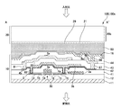
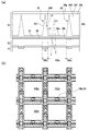
(画素の具体的構成)
図3は、本発明を適用した液晶装置の画素1つ分の断面図である。図4(a)、(b)は各々、本発明を適用した液晶装置に用いた素子基板において相隣接する画素の平面図、およびこの素子基板上における遮光領域を右上がりの斜線によって示した説明図である。図3は、図4(a)のA−A′線に相当する位置で液晶装置100を切断したときの断面図に相当する。なお、図4(a)、(b)では、半導体層は細くて短い点線で示し、走査線3aは太い実線で示し、データ線6aおよびそれと同時形成された薄膜は一点鎖線で示し、容量線5bは二点鎖線で示し、画素電極9aおよびそれと同時形成された薄膜は太くて長い点線で示し、後述する中継電極は細い実線で示してある。
(Specific pixel configuration)
FIG. 3 is a cross-sectional view of one pixel of a liquid crystal device to which the present invention is applied. 4A and 4B are respectively a plan view of adjacent pixels in an element substrate used in a liquid crystal device to which the present invention is applied, and an explanation in which a light-shielding region on the element substrate is indicated by a diagonal line rising to the right. FIG. 3 corresponds to a cross-sectional view when the
図3および図4(a)に示すように、素子基板10上には、複数の画素100aの各々に矩形状の画素電極9aが形成されており、各画素電極9aの縦横の境界に各々沿ってデータ線6aおよび走査線3aが形成されている。データ線6aおよび走査線3aは各々、直線的に延びている。また、データ線6aと走査線3aとが交差する領域に電界効果型トランジスタ30が形成されている。また、素子基板10上には、走査線3aと重なるように容量線5bが形成されている。本形態において、容量線5bは、走査線3aと重なるように直線的に延びた主線部分と、データ線6aと走査線3aとの交差部分でデータ線6aに重なるように延びた副線部分とを備えている。
As shown in FIG. 3 and FIG. 4A, a
素子基板10は、石英基板やガラス基板などの透光性材料からなる支持基板11(基板本体)、その液晶層50側の表面に形成された画素電極9a、画素スイッチング用の電界効果型トランジスタ30、および配向膜16を主体として構成されており、対向基板20は、後述する偏向用基板20b、その液晶層50側表面に形成された共通電極21、および配向膜29を主体として構成されている。
The
素子基板10において、画素電極9aに隣接する位置には電界効果型トランジスタ30が形成されている。電界効果型トランジスタ30は、例えば、LDD(Lightly Doped Drain)構造を有しており、半導体層1aには、走査線3aに対してゲート絶縁層2を介して対向するチャネル領域1a′、低濃度ソース領域1b、低濃度ドレイン領域1c、高濃度ソース領域1dおよび高濃度ドレイン領域1eが形成されている。
In the
半導体層1aは、例えば、石英基板からなる支持基板11上に下地絶縁膜12を介して形成された単結晶シリコン層によって構成され、このような構成の素子基板10は、石英基板と単結晶シリコン基板とが絶縁層を介して貼り合わされたSOI(Silicon On Insulator)基板を用いることにより実現することができる。このようなSOI基板は、例えば、単結晶シリコン基板上にシリコン酸化膜を形成した上で石英基板と貼り合わせる方法、あるいは石英基板と単結晶シリコン基板の双方にシリコン酸化膜を形成した上でシリコン酸化膜同士を接触させて貼り合わせる方法を採用できる。このような基板を用いた場合、ゲート絶縁層2(第2絶縁膜)は、半導体層1aに対する熱酸化膜により形成できる。走査線3aには、ポリシリコンやアモルファスシリコン、単結晶シリコン膜などのシリコン膜や、これらのポリサイドやシリサイド、さらには金属膜が用いられる。
The
走査線3aの上層側には、高濃度ソース領域1dへ通じるコンタクトホール82、および高濃度ドレイン領域1eへ通じるコンタクトホール83を備えたシリコン酸化膜などからなる第1層間絶縁膜41が形成されている。第1層間絶縁膜41の上層には中継電極4a、4bが形成されている。中継電極4aは、走査線3aとデータ線6aとの交差する位置を基点として走査線3aおよびデータ線6aに沿って延出する略L字型に形成されており、中継電極4bは、中継電極4bと離間した位置において、データ線6aに沿うように形成されている。中継電極4aは、コンタクトホール83を介して高濃度ドレイン領域1eに電気的に接続され、中継電極4bは、コンタクトホール82を介して高濃度ソース領域1dに電気的に接続されている。
On the upper layer side of the
中継電極4a、4bの上層側には、シリコン窒化膜などからなる誘電体膜42が形成されており、この誘電体膜42を介して、中継電極4aと対向するように容量線5bが形成され、蓄積容量55が形成されている。中継電極4a、4bは導電性のポリシリコン膜や金属膜等からなり、容量線5bは、導電性のポリシリコン膜、高融点金属を含む金属シリサイド膜、それらの積層膜、金属膜からなる。
A
容量線5bの上層側には、中継電極4aへ通じるコンタクトホール87、および中継電極4bへ通じるコンタクトホール81を備えたシリコン酸化膜などからなる第2層間絶縁膜43が形成されている。第2層間絶縁膜43の上層にはデータ線6aおよびドレイン電極6bが形成されている。データ線6aはコンタクトホール81を介して中継電極4bに電気的に接続し、中継電極4bを介して高濃度ソース領域1dに電気的に接続している。ドレイン電極6bはコンタクトホール87を介して中継電極4aに電気的に接続し、中継電極4aを介して、高濃度ドレイン領域1eに電気的に接続している。データ線6aおよびドレイン電極6bは、導電性のポリシリコン膜、高融点金属を含む金属シリサイド膜、それらの積層膜、金属膜からなる。
On the upper layer side of the
データ線6aおよびドレイン電極6bの上層側には、シリコン酸化膜などからなる第3層間絶縁膜44が形成されている。第3層間絶縁膜44には、ドレイン電極6bへ通じるコンタクトホール86が形成されている。
A third
第3層間絶縁膜44の上層には、ITO(Indium Tin Oxide)膜などからなる透光性の画素電極9aが形成されており、画素電極9aは、コンタクトホール86を介してドレイン電極6bに電気的に接続されている。画素電極9aの表面には配向膜16が形成されている。
A
これに対して、対向基板20では、偏向用基板20bにおいて素子基板10と対向する面側に共通電極21および配向膜29が形成されている。
In contrast, in the
このように構成した液晶装置100においては、走査線3a、容量線5b、データ線6aおよび電界効果型トランジスタ30の形成領域によって、表示に直線寄与しない格子状の遮光領域100c(図4(b)に右上がりの斜線を付した領域)が形成されており、かかる遮光領域100cは、互いに交差する第1方向(矢印Xで示す方向)および第2方向(矢印Yで示す方向)に延在し、かかる遮光領域100cで周りが囲まれた領域が、変調光を出射して表示に直接寄与する画素開口領域100dになっている。本形態では、対向基板20には、いわゆるブラックマトリクスやブラックストライプと称せられる遮光膜が形成されていない。このため、遮光領域100cは、走査線3a、容量線5b、データ線6aおよび電界効果型トランジスタ30の形成領域によって規定されている。
In the
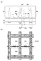
(偏向用基板20bの構成)
図5(a)、(b)は各々、本発明の実施の形態1に係る液晶装置の断面を模式的に示して偏向用基板の断面構成を示す説明図、および偏向用基板の偏向部の平面構成を示す説明図である。なお、図5(a)では、素子基板10側の配向膜16などの図示を省略してある。
(Configuration of
5 (a) and 5 (b) are explanatory diagrams schematically showing a cross-sectional configuration of the deflection substrate by schematically showing a cross section of the liquid crystal device according to the first embodiment of the present invention, and a deflection unit of the deflection substrate. It is explanatory drawing which shows a plane structure. In FIG. 5A, the
図5(a)、(b)に示すように、本形態の液晶装置100においては、対向基板20の側から入射した光を液晶層50によって画素毎に光変調した後、素子基板10から出射する。このため、入射光を効率よく利用するには、入射光を画素開口領域100dに効率よく導く必要がある。そこで、本形態では、対向基板20に偏向用基板20bが用いられており、かかる偏向用基板20bでは、変調すべき光が入射する側に斜面を向けて光を画素開口領域100dに向けて導く断面V字形状の偏向部26が遮光領域100cと重なる領域に沿って形成されている。
As shown in FIGS. 5A and 5B, in the
より具体的には、偏向用基板20bにおいて、その母材である透光性基板20fの変調すべき光が入射する側の面20g(液晶層50が位置する側とは反対側)には、エポキシ樹脂やアクリル樹脂などの樹脂材料、あるいは低融点ガラスからなる透光性の被転写層20hが形成されており、被転写層20hには、変調すべき光が入射する側に向かって尖った断面V字形状の偏向突起261が形成されている。また、透光性基板20fの面20g側では、被転写層20hを完全に覆うように、被転写層20hよりも屈折率の高い高屈折率層20iが形成されており、偏向突起261の斜面262は、高屈折率層20iで覆われている。高屈折率層20iにおいて、変調すべき光が入射する側の面20jは平坦面になっている。
More specifically, in the
本形態において、高屈折率層20iは、被転写層20hを構成する材料の屈折率に応じて、シリコン窒化膜や金属酸化膜などの高屈折材料から選択された材料からなり、斜面262に反射性を付与している。
In this embodiment, the high
すなわち、高屈折率層20iを構成する材料の屈折率をn11とし、被転写層20hを構成する材料の屈折率をn12とし、斜面262の法線に対する光の入射角度をθ0とした場合、n11>n12で、かつ、n11、n12、θ0が以下の式
sinθ0>n12/n11
を満たせば、全反射が起こるので、斜面262に反射性を付与することができる。
That is, the refractive index of the material constituting the high
If this condition is satisfied, total reflection occurs, so that the
なお、透光性基板20fにおいて、液晶層50が位置する側の面20kは、平滑面になっており、その表面に対向電極21および配向膜29が形成されている。
In the
(偏向用基板20bの作用効果)
このように構成した液晶装置100では、図1を参照して説明した光源部140からは様々な入射角度の光が入射し、かかる入射光のうち、画素開口領域100dに向かう光は、矢印L1で示すように、そのまま進行する一方、矢印L2で示すように、画素開口領域100dに向かう方向から外れた方向に向かう光については、矢印L3で示すように、偏向部26の反射性の斜面262で反射させ、画素開口領域100dに向かわせる。
(Operational effect of the
In the
ここで、偏向部26は、斜面262を一辺とする略二等辺三角形形状の断面を有する偏向突起261からなり、三角形形状の頂点は、遮光領域100cの幅方向の中心に位置している。また、偏向部26(偏向突起261)の幅寸法(三角形形状の底辺の長さ)は、遮光領域100cの幅寸法と略同一寸法、あるいはやや幅広に設定されており、これにより、画素開口領域100dに向かう方向から外れた方向に向かう光についても有効に利用することができる。なお、斜面262の傾きについては、特開2006−215427号公報に開示されているように、例えば、透光性基板20fの基板面に対する法線となす角度が3°以下になるように設定される。かかる構成によれば、斜面262で光を反射した際、光線角度の増大を低減しながら入射光を偏向することができるとともに、入射光を、例えば、Fナンバーが2.5である投射光学系(図1参照)で十分取り込むことが可能な光線角度の光に変換することができ、コントラストの向上および入射光を利用効率の向上を図ることができる。
Here, the
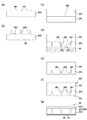
(偏向用基板20bおよび対向基板20の製造方法)
図6を参照して、本形態の液晶装置100の製造工程のうち、偏向用基板20bおよび対向基板20の製造工程を説明する。図6は、本形態の液晶装置100に用いた偏向用基板20bおよび対向基板20の製造工程を示す工程断面図である。
(Manufacturing method of the
With reference to FIG. 6, the manufacturing process of the deflection | deviation board |
本形態の偏向用基板20bおよび対向基板20を製造するには、まず、図6(a)、(b)に示す工程により、転写用の型部材61を形成する。それには、図6(a)に示すように、型部材61の基材として、シリコン基板、石英基板、ニッケルなどの金属基板などからなる板材610を準備した後、フォトリソグラフィ技術を利用して、その一方の面611に、厚さが50〜200μmのレジストマスク62を形成する。次に、板材610に対してドライエッチングを行なう。かかるドライエッチングには、高密度プラズマを形成可能なICPドライエッチング装置を用い、板材610とレジストマスク62とのエッチング選択比を例えば4:1とする。その結果、図6(b)に示すように、レジストマスク62の厚みに対して略4倍の深さを有する断面V字形状の溝612が形成される。このようにして、成形面613に断面V字形状の溝612を備えた型部材61を得ることができ、かかる溝612の形状は、図5(a)を参照して説明した偏向突起261の形状に対応している。
In order to manufacture the
かかる型部材61を用いて偏向用基板20bを製造するには、まず、図6(c)に示す被転写層形成工程において、偏向用基板20bの母材たる透光性基板20fの一方の面20gに、エポキシ樹脂やアクリル樹脂などの樹脂材料、あるいは低融点ガラスからなる透光性の被転写層20hを形成する。かかる材料のうち、熱硬化性樹脂を用いた場合には、ある程度、軟性をもった状態に硬化を止めておく。
In order to manufacture the
次に、図6(d)に示す転写工程において、被転写層20hを加熱するなどの方法で軟化性を示す状態とした後、被転写層20hに型部材61の成形面613を押し付けて、溝612の反転パターンを被転写層20hに転写する。次に、被転写層20hを固化させた後、型部材61を外すと、図6(e)に示すように、被転写層20hには、斜面262を備えた偏向突起261が形成される。なお、転写の際、型部材61の成形面613に離型剤を塗布しておくと、型部材61を容易に外すことができ、偏向突起261の形状が崩れない。
Next, in the transfer step shown in FIG. 6 (d), after the
次に、図6(f)に示す反射性付与工程では、被転写層20hを完全に覆うように、被転写層20hよりも屈折率の高い高屈折率層20iを形成する。その結果、偏向突起261の斜面262は、高屈折率層20iで覆われ、斜面262に反射性が付与される。
Next, in the reflectivity imparting step shown in FIG. 6F, the high
次に、図6(g)に示す研磨工程では、透光性基板20fの面20kを研磨し、透光性基板20fの薄板化を行なうとともに、面20kを平滑化する。かかる研磨工程において、本形態では、化学機械研磨を行なう。この化学機械研磨では、研磨液に含まれる化学成分の作用と、研磨剤と透光性基板20fとの相対移動によって、高速で平滑な研磨面を得ることができる。より具体的には、研磨装置において、不織布、発泡ポリウレタン、多孔質フッ素樹脂などからなる研磨布(パッド)を貼り付けた定盤と、透光性基板20fを保持するホルダとを相対回転させながら、研磨を行なう。その際、例えば、平均粒径が0.01〜20μmの酸化セリウム粒子、分散剤としてのアクリル酸エステル誘導体、および水を含む研磨剤を研磨布と透光性基板20fとの間に供給する。なお、被転写層20hの表面にも研磨を施して平滑化してもよい。
Next, in the polishing step shown in FIG. 6G, the
次に、図6(h)に示すように、透光性基板20fの面20k側に対向電極21および配向膜29を形成し、対向基板20を得る。
Next, as illustrated in FIG. 6H, the
(本形態の主な効果)
以上説明したように、本形態では、偏向用基板20bを得るにあたって、透光性基板20f上に透光性の被転写層20hを形成した後、型部材61において偏向突起261の形状に対応する溝612を備えた成形面613を押し付けて溝612の反転パターンを被転写層20hに転写し、斜面262を備えた偏向突起261を形成する。このため、偏向用基板20bの斜面262をエッチングで形成する必要がないので、偏向用基板20bを効率よく製造することができ、かつ、偏向突起261の斜面262については、傾き角度の精度が高く、ばらつきが発生しない。
(Main effects of this form)
As described above, in this embodiment, in obtaining the
また、本形態では、断面V字形状の偏向部26によって入射光を画素開口領域100dに導くため、対向基板20には、ブラックマトリクスやブラックストライプなどと称せられる遮光層を設ける必要がないので、その分、製造工程数を減らすことができる。
In this embodiment, since the incident light is guided to the
[実施の形態2]
(偏向用基板20bの構成)
図7(a)、(b)は各々、本発明の実施の形態2に係る液晶装置の断面を模式的に示して偏向用基板の断面構成を示す説明図、および偏向用基板の偏向部の平面構成を示す説明図である。なお、図7(a)では、素子基板10側の配向膜16などの図示を省略してある。また、本形態の基本的な構成は、実施の形態1と同様であるため、共通する部分には同一の符号を付して図示し、それらの説明を省略する。
[Embodiment 2]
(Configuration of
FIGS. 7 (a) and 7 (b) are schematic diagrams showing the cross section of the liquid crystal device according to the second embodiment of the present invention, showing the cross-sectional configuration of the deflection substrate, and the deflection unit of the deflection substrate. It is explanatory drawing which shows a plane structure. In FIG. 7A, illustration of the
図7(a)、(b)に示すように、本形態の液晶装置100においても、実施の形態1と同様、対向基板20の側から入射した光を液晶層50によって画素毎に光変調した後、素子基板10から出射する。また、本形態でも、実施の形態1と同様、対向基板20に偏向用基板20bが用いられており、かかる偏向用基板20bでは、変調すべき光が入射する側に斜面を向けて光を画素開口領域100dに向けて導く断面V字形状の偏向部26が遮光領域100cと重なる領域に沿って形成されている。
As shown in FIGS. 7A and 7B, in the
より具体的には、偏向用基板20bにおいて、その母材である透光性基板20fの変調すべき光が出射する側の面20k(液晶層50が位置する側の面)には、エポキシ樹脂やアクリル樹脂などの樹脂材料、あるいは低融点ガラスからなる透光性の被転写層20hが形成されており、被転写層20hには、変調すべき光が入射する側に向かって凹んだ断面V字形状の偏向溝266が形成されている。また、透光性基板20fの面20kの側では、被転写層20hを完全に覆うように、被転写層20hよりも屈折率の低い低屈折率層20sが形成されており、偏向溝266の斜面267は、低屈折率層20sで覆われている。低屈折率層20sにおいて、変調すべき光が出射する側の面20tは平滑面になっており、その表面に対向電極21および配向膜29が形成されている。
More specifically, in the
本形態において、低屈折率層20sは、被転写層20hを構成する材料の屈折率に応じて、シリコン酸化膜、その他の金属酸化膜、あるいは樹脂により構成されており、斜面267に反射性を付与している。
In this embodiment, the low
すなわち、被転写層20hを構成する材料の屈折率をn21とし、低屈折率層20sを構成する材料の屈折率をn22とし、斜面267の法線に対する光の入射角度をθ0とした場合、n21>n22で、かつ、n21、n22、θ0が以下の式
sinθ0>n22/n21
を満たせば、全反射が起こるので、斜面267に反射性を付与することができる。
That is, the refractive index of the material constituting the transferred
If the above condition is satisfied, total reflection occurs, so that the
なお、透光性基板20fにおいて、変調すべき光が出射する側の面20g(液晶層50が位置する側とは反対側の面)は平滑面になっている。
In the
このように構成した液晶装置100でも、実施の形態1と同様、図1を参照して説明した光源部140からは様々な入射角度の光が入射し、かかる入射光のうち、画素開口領域100dに向かう光は、矢印L1で示すように、そのまま進行させる一方、矢印L2で示すように、画素開口領域100dに向かう方向から外れた方向に向かう光については、矢印L3で示すように、偏向部26の反射性の斜面267で反射させ、画素開口領域100dに向かわせる。
In the
ここで、偏向部26は、斜面267を一辺とする略二等辺三角形形状の断面の偏向溝266からなり、三角形形状の頂点は、遮光領域100cの幅方向の中心に位置している。また、偏向部26の幅寸法(三角形形状の底辺の長さ)は、遮光領域100cの幅寸法と略同一寸法、あるいはやや幅広に設定されており、これにより、画素開口領域100dに向かう方向から外れた方向に向かう光についても有効に利用することができる。なお、斜面267の傾きについては、特開2006−215427号公報に開示されているように、例えば、透光性基板20fの基板面に対する法線となす角度が3°以下になるように設定される。かかる構成によれば、斜面267で光を反射した際、光線角度の増大を低減しながら入射光を偏向することができるとともに、入射光を、例えば、Fナンバーが2.5である投射光学系(図1参照)で十分取り込むことが可能な光線角度の光に変換することができ、コントラストの向上および入射光を利用効率の向上を図ることができる。
Here, the
(偏向用基板20bおよび対向基板20の製造方法)
図8を参照して、本形態の液晶装置100の製造工程のうち、偏向用基板20bおよび対向基板20の製造工程を説明する。図7は、本形態の液晶装置100に用いた偏向用基板20bおよび対向基板20の製造工程を示す工程断面図である。
(Manufacturing method of the
With reference to FIG. 8, the manufacturing process of the deflection | deviation board |
本形態の偏向用基板20bおよび対向基板20を製造するには、まず、図8(a)、(b)に示す工程により、転写用の型部材66を形成する。それには、図8(a)に示すように、型部材66の基材として、シリコン基板、石英基板、ニッケルなどの金属基板などからなる板材660を準備した後、フォトリソグラフィ技術を利用して、その一方の面661に、厚さが50〜200μmのレジストマスク67を形成する。次に、板材660に対してドライエッチングを行なう。かかるドライエッチングには、高密度プラズマを形成可能なICPドライエッチング装置を用い、板材660とレジストマスク67とのエッチング選択比を例えば4:1とする。その結果、図8(b)に示すように、レジストマスク67の厚みに対して略4倍の深さを有する断面V字形状の突起662が形成される。このようにして、成形面663に断面V字形状の突起662を備えた型部材66を得ることができ、かかる突起662の形状は、図7(a)を参照して説明した偏向溝266の形状に対応している。
In order to manufacture the
かかる型部材66を用いて偏向用基板20bを製造するには、まず、図8(c)に示す被転写層形成工程において、偏向用基板20bの母材たる透光性基板20fの一方の面20kに、エポキシ樹脂やアクリル樹脂などの樹脂材料、あるいは低融点ガラスからなる透光性の被転写層20hを形成する。
In order to manufacture the
次に、図8(d)に示す転写工程において、被転写層20hが軟化している状態で、型部材66の成形面663を押し付けて、突起662の反転パターンを被転写層20hに転写する。次に、被転写層20hを固化させた後、型部材66を外すと、図8(e)に示すように、被転写層20hには、斜面267を備えた偏向溝266が形成される。なお、転写の際、型部材66の成形面663に離型剤を塗布しておくと、型部材66を容易に外すことができ、偏向溝266の形状が崩れない。
Next, in the transfer step shown in FIG. 8D, with the transferred
次に、図8(f)に示す反射性付与工程では、被転写層20hを完全に覆うように、被転写層20hよりも屈折率の低い低屈折率層20sを形成する。その結果、偏向溝266の斜面267は、低屈折率層20sで覆われ、斜面267に反射性が付与される。
Next, in the reflectivity imparting step shown in FIG. 8 (f), a low
次に、図8(g)に示す研磨工程では、透光性基板20fの他方の面20gを研磨し、透光性基板20fの薄板化を行なうとともに、面20gを平滑化する。また、低屈折率層20sにおいて、変調すべき光が出射する側の面20tにも研磨を行い、平滑化してもよい。かかる研磨工程において、本形態では、実施の形態1と同様、化学機械研磨を行なう。次に、低屈折率層20sの面20t側に対向電極21および配向膜29を形成し、対向基板20を得る。
Next, in the polishing step shown in FIG. 8G, the
(本形態の主な効果)
以上説明したように、本形態では、偏向用基板20bを得るにあたって、透光性基板20f上に透光性の被転写層20hを形成した後、型部材66において偏向溝266の形状に対応する突起662を備えた成形面663を押し付けて突起662の反転パターンを被転写層20hに転写し、斜面267を備えた偏向溝266を形成する。このため、偏向用基板20bの斜面267をエッチングで形成する必要がないので、偏向用基板20bを効率よく製造することができ、かつ、偏向突起261の斜面267については、傾き角度の精度が高く、ばらつきが発生しない。
(Main effects of this form)
As described above, in this embodiment, in obtaining the
また、本形態では、断面V字形状の偏向部26によって入射光を画素開口領域100dに導くため、対向基板20には、ブラックマトリクスやブラックストライプなどと称せられる遮光層を設ける必要がないので、その分、製造工程数を減らすことができる。
In this embodiment, since the incident light is guided to the
[実施の形態2の変形例]
実施の形態2では、被転写層20hを完全に覆うように低屈折率層20sを形成したが、偏向溝266内のみに低屈折率層20sを充填してもよい。また、実施の形態2では、偏向溝662内に酸化膜や樹脂などの低屈折材料を充填したが、図9に示すように、偏向溝662に低屈折率材料として空気268を充填しても、斜面267に反射性を付与することができる。かかる構成は、例えば、減圧雰囲気下で被転写層20hに接着剤20vを介して透光性のカバー基板20wを貼り付けることにより、実現することができる。
[Modification of Embodiment 2]
In the second embodiment, the low
[他の偏向用基板20bの製造方法]
上記実施の形態1、2では、研磨工程で透光性基板20fを残したが、透光性基板20fを完全に除去してもよい。また、上記形態では、型部材61、66の形成にドライエチングを用いたが、レーザエッチングを行なってもよい。
[Manufacturing Method of Another
In the first and second embodiments, the
上記実施の形態1、2では、斜面262、267に反射性を付与するにあたって、屈折率の差を利用したが、斜面262、267を覆うように、アルミニウム、アルミニウム合金、銀、銀合金などといった光反射性材料層を形成してもよい。この場合、実施の形態1では、斜面262のみに光反射性材料層を形成する。これに対して、実施の形態2では、斜面267のみに光反射性材料層を形成した構成、あるいは偏向溝266を光反射性材料層で埋めた構成のいずれを採用してもよい。
In the first and second embodiments, the difference in refractive index is used to provide reflectivity to the
また、上記実施の形態では、偏向突起261や偏向溝266の断面が二等辺三角形である例を説明したが、図10(a)に示すように、二等辺三角形の頂部が丸まっている構成や、図10(b)に示すように、斜面262、267が、透光性基板20fの基板面に対する法線方向に対して異なる傾きの第1斜面268と第2斜面269を有する構成を採用してもよい。ここで、二等辺三角形の底部側に位置する第2斜面269が、第1斜面268に比して、透光性基板20fの基板面に対する法線方向に対して大きな角度を形成していれば、液晶のドメインなどが発生しやすい画素開口領域100dの端部分を避けて、画素開口領域100dの中央に入射光を導くことができる。
In the above embodiment, an example in which the cross section of the
また、上記実施の形態では、対向基板20にブラックマトリクスあるいはブラックマトリクスと称せられる遮光層を省略したが、かかる遮光層を設けてもよい。
In the above embodiment, the light shielding layer referred to as a black matrix or a black matrix is omitted from the
[他の実施の形態]
図1には、ライトバルブを3枚用いた投射型表示装置を例示したが、液晶装置100がカラーフィルタを内蔵している場合、図11に示す投射型表示装置において、本発明を適用した1枚の液晶装置100をライトバルブとして用いて、カラー画像をスクリーン211に投射表示するように構成してもよい。すなわち、図11に示す投射型表示装置210は、白色光源212、インテグレータ221および偏光変換素子222を備えた光源部240と、液晶装置100と、投射光学系218とを備えている。また、液晶装置100では、カラーフィルタ内蔵の液晶パネル100xの両側に第1偏光板216aおよび第2偏光板216bが配置されている。
[Other embodiments]
FIG. 1 illustrates a projection display device using three light valves. However, when the
また、上記形態では、電気光学装置として、投射型表示装置に用いる透過型の液晶装置を例示したが、投射型表示装置に用いる反射型の液晶装置に本発明を適用してもよい。また、バックライト装置から出射された光を入射光として画像を表示する直視型の透過型あるいは半透過反射型の液晶装置や、外光を入射光として画像を表示する直視型の反射型の液晶装置に本発明を適用してもよい。 In the above embodiment, the transmissive liquid crystal device used in the projection display device is exemplified as the electro-optical device. However, the present invention may be applied to a reflective liquid crystal device used in the projection display device. Also, a direct-view transmissive or transflective liquid crystal device that displays an image using light emitted from a backlight device as incident light, and a direct-view reflective liquid crystal device that displays images using external light as incident light. The present invention may be applied to an apparatus.
さらに、上記形態では、電気光学装置として液晶装置を例に説明したが、自発光素子から出射された変調光によって画像表示面で画像を表示する電気光学装置において混色などを防止することを目的に、縦横に延在する格子状の遮光領域を設け、この遮光領域で囲まれた画素開口領域から変調光を出射する電気光学装置に本発明を適用してもよい。 Furthermore, in the above embodiment, the liquid crystal device has been described as an example of the electro-optical device, but for the purpose of preventing color mixing or the like in the electro-optical device that displays an image on the image display surface by the modulated light emitted from the self-light emitting element. Alternatively, the present invention may be applied to an electro-optical device in which a grid-like light shielding region extending in the vertical and horizontal directions is provided and modulated light is emitted from a pixel opening region surrounded by the light shielding region.
10・・素子基板、20・・対向基板、20b・・偏向用基板、20f・・透光性基板、20h・・被転写層、20i・・高屈折率層、20s・・低屈折率層、26・・偏向部、61、66・・型部材、100・・液晶装置(電気光学装置)、100c・・遮光領域、100d・・画素開口領域、261・・偏向突起、262、267・・斜面、266・・偏向溝
10..Element substrate, 20..Counter substrate, 20b..Deflection substrate, 20f..Translucent substrate, 20h..Transfer layer, 20i..High refractive index layer, 20s..Low refractive index layer, ··· Deflection part, 61, 66 ·· Mold member, 100 ·· Liquid crystal device (electro-optical device), 100c ·· Light-shielding region, 100d ·· Pixel opening region, 261 ·· Deflection protrusion, 262, 267 ··
Claims (8)
透光性基板上に透光性の被転写層を形成する被転写層形成工程と、
型部材の凹凸を備えた成形面を押し付けて前記凹凸の反転パターンを前記被転写層に転写して前記断面V字形状の一対の斜面を形成する転写工程と、
前記一対の斜面に反射性を付与する反射性付与工程と、
を行なうことを特徴とする電気光学装置の製造方法。 In the manufacturing method for an electro-optical device having a pair of slope shape made the board of V-shaped cross section for guiding incident light to the pixel opening region,
A transferred layer forming step of forming a transparent transferred layer on the transparent substrate;
A transfer step of pressing a molding surface having projections and depressions of a mold member to transfer a reverse pattern of the projections and depressions to the transfer layer to form a pair of inclined surfaces having a V-shaped cross section ;
A reflectivity imparting step for imparting reflectivity to the pair of slopes;
A method for manufacturing an electro-optical device.
被転写層形成工程では、被転写層を軟性をもった状態に止めておき、
前記転写工程後に、前記被転写層を硬化することを特徴とする請求項1に記載の電気光学装置の製造方法。 The transferred layer is a thermosetting resin,
In the transferred layer forming step, the transferred layer is kept in a soft state,
The method of manufacturing an electro-optical device according to claim 1, wherein the transfer layer is cured after the transfer step.
前記凹凸の反転パターンを前記被転写層に転写する前に、前記被転写層を加熱して、前記被転写層を軟性を示す状態とし、
前記凹凸の反転パターンを前記被転写層に転写した後、前記被転写層を硬化することを特徴とする請求項1に記載の電気光学装置の製造方法。 In the transferred layer forming process,
Before transferring the reverse pattern of the unevenness to the transferred layer, the transferred layer is heated to bring the transferred layer into a state of showing flexibility.
The method of manufacturing an electro-optical device according to claim 1, wherein the transferred layer is cured after the reverse pattern of the unevenness is transferred to the transferred layer.
前記型部材には、当該突起に対応する断面V字形状の溝が形成されており、
前記反射性付与工程では、前記突起の前記斜面を覆うように、前記被転写層より屈折率の高い高屈折率層、あるいは光反射性材料層を形成することを特徴とする請求項1乃至3のいずれかに記載の電気光学装置の製造方法。 A pair of inclined surfaces of the V-shaped cross section is an impact caused the light to be modulated is pointed toward the side where the incident,
The mold member has a groove is formed in the V-shaped cross section corresponding to those of the protrusion,
In the reflective-imparting step, before Ki突 to cover the slopes of force, according to claim 1, characterized in that forming the higher refractive index than the transfer layer high refractive index layer, or a light reflective material layer 4. A method for manufacturing an electro-optical device according to any one of items 1 to 3.
前記型部材には、当該溝に対応する断面V字形状の突起が形成されており、
前記反射性付与工程では、前記溝内に前記斜面を覆うように、前記被転写層より屈折率の低い低屈折率層、あるいは光反射性材料層を形成することを特徴とする請求項1乃至3のいずれかに記載の電気光学装置の製造方法。 The pair of inclined surfaces having a V-shaped cross section are grooves recessed toward the side on which light to be modulated is incident,
The mold member, the projection is formed of a V-shaped cross section corresponding to those of the groove,
Wherein the reflective application step, so as to cover the inclined surface before the Kimizo, claim 1, wherein the forming the lower low refractive index layer having a refractive index than the transfer layer, or a light reflective material layer 4. A method for manufacturing an electro-optical device according to any one of items 1 to 3.
Priority Applications (1)
| Application Number | Priority Date | Filing Date | Title |
|---|---|---|---|
| JP2007250783A JP5125357B2 (en) | 2007-09-27 | 2007-09-27 | Manufacturing method of electro-optical device |
Applications Claiming Priority (1)
| Application Number | Priority Date | Filing Date | Title |
|---|---|---|---|
| JP2007250783A JP5125357B2 (en) | 2007-09-27 | 2007-09-27 | Manufacturing method of electro-optical device |
Publications (3)
| Publication Number | Publication Date |
|---|---|
| JP2009080388A JP2009080388A (en) | 2009-04-16 |
| JP2009080388A5 JP2009080388A5 (en) | 2010-08-19 |
| JP5125357B2 true JP5125357B2 (en) | 2013-01-23 |
Family
ID=40655161
Family Applications (1)
| Application Number | Title | Priority Date | Filing Date |
|---|---|---|---|
| JP2007250783A Expired - Fee Related JP5125357B2 (en) | 2007-09-27 | 2007-09-27 | Manufacturing method of electro-optical device |
Country Status (1)
| Country | Link |
|---|---|
| JP (1) | JP5125357B2 (en) |
Families Citing this family (1)
| Publication number | Priority date | Publication date | Assignee | Title |
|---|---|---|---|---|
| JP5737037B2 (en) * | 2011-07-22 | 2015-06-17 | セイコーエプソン株式会社 | Electro-optical device and projection display device |
Family Cites Families (5)
| Publication number | Priority date | Publication date | Assignee | Title |
|---|---|---|---|---|
| JPH09251162A (en) * | 1996-03-15 | 1997-09-22 | Matsushita Electron Corp | Image display device provided with condensing element |
| JP3826649B2 (en) * | 2000-01-18 | 2006-09-27 | セイコーエプソン株式会社 | Electro-optical device and projection display device |
| JP5027969B2 (en) * | 2001-08-27 | 2012-09-19 | 大日本印刷株式会社 | Manufacturing method of two-dimensional field expansion member |
| JP2004361821A (en) * | 2003-06-06 | 2004-12-24 | Seiko Epson Corp | Spatial light modulator and projector |
| JP4876613B2 (en) * | 2006-02-15 | 2012-02-15 | セイコーエプソン株式会社 | Electro-optical device, method for manufacturing electro-optical device, projector, and electronic apparatus |
-
2007
- 2007-09-27 JP JP2007250783A patent/JP5125357B2/en not_active Expired - Fee Related
Also Published As
| Publication number | Publication date |
|---|---|
| JP2009080388A (en) | 2009-04-16 |
Similar Documents
| Publication | Publication Date | Title |
|---|---|---|
| JP6167740B2 (en) | Electro-optical device substrate, electro-optical device, and electronic apparatus | |
| JP6880701B2 (en) | Electro-optics and electronic equipment | |
| JP6111601B2 (en) | Microlens array substrate, microlens array substrate manufacturing method, electro-optical device, and electronic apparatus | |
| JP6123317B2 (en) | Liquid crystal device and electronic device | |
| JP6337604B2 (en) | Electro-optical device manufacturing method, electro-optical device, and electronic apparatus | |
| JP6318881B2 (en) | Microlens array substrate, microlens array substrate manufacturing method, electro-optical device, and electronic apparatus | |
| JP5845679B2 (en) | Electro-optical device, method of manufacturing electro-optical device, and projection display device | |
| JP5737037B2 (en) | Electro-optical device and projection display device | |
| JP2015129894A (en) | Microlens array, method for manufacturing microlens array, electro-optic device, and electronic apparatus | |
| JP2016151735A (en) | Lens array substrate, electro-optic device, electronic apparatus, and method for manufacturing lens array substrate | |
| JP2015022100A (en) | Electro-optic device, method for manufacturing electro-optic device, and electronic equipment | |
| JP2014092601A (en) | Method for manufacturing microlens array substrate, microlens array substrate, electro-optic device, and electronic equipment | |
| JP5076838B2 (en) | Color filter substrate, electro-optical device, and method for manufacturing color filter substrate | |
| CN101017275B (en) | Converging substrate, electro-optic device, substrate for electro-optic device, projector, and electronic apparatus | |
| JP6398361B2 (en) | Microlens array substrate, electro-optical device, and electronic device | |
| JP5125357B2 (en) | Manufacturing method of electro-optical device | |
| JP6318946B2 (en) | Microlens array substrate, electro-optical device, and electronic device | |
| JP5029209B2 (en) | Electro-optical device and projection display device | |
| JP6414256B2 (en) | Microlens array substrate, microlens array substrate manufacturing method, electro-optical device, and electronic apparatus | |
| JP4872870B2 (en) | Electro-optical device, method of manufacturing electro-optical device, and projection display device | |
| JP6299493B2 (en) | Microlens array substrate, electro-optical device, and electronic device | |
| JP6364912B2 (en) | Microlens array substrate, electro-optical device, and electronic device | |
| JP7200979B2 (en) | liquid crystal devices and electronic devices | |
| US11163190B2 (en) | Electro-optical device and electronic apparatus | |
| JP2018072756A (en) | Microlens array substrate and method for manufacturing the same, electro-optical device and method for manufacturing the same, and electronic apparatus |
Legal Events
| Date | Code | Title | Description |
|---|---|---|---|
| A521 | Written amendment |
Free format text: JAPANESE INTERMEDIATE CODE: A523 Effective date: 20100707 |
|
| A621 | Written request for application examination |
Free format text: JAPANESE INTERMEDIATE CODE: A621 Effective date: 20100707 |
|
| A131 | Notification of reasons for refusal |
Free format text: JAPANESE INTERMEDIATE CODE: A131 Effective date: 20120124 |
|
| A977 | Report on retrieval |
Free format text: JAPANESE INTERMEDIATE CODE: A971007 Effective date: 20120125 |
|
| A521 | Written amendment |
Free format text: JAPANESE INTERMEDIATE CODE: A523 Effective date: 20120306 |
|
| TRDD | Decision of grant or rejection written | ||
| A01 | Written decision to grant a patent or to grant a registration (utility model) |
Free format text: JAPANESE INTERMEDIATE CODE: A01 Effective date: 20121002 |
|
| A01 | Written decision to grant a patent or to grant a registration (utility model) |
Free format text: JAPANESE INTERMEDIATE CODE: A01 |
|
| A61 | First payment of annual fees (during grant procedure) |
Free format text: JAPANESE INTERMEDIATE CODE: A61 Effective date: 20121015 |
|
| R150 | Certificate of patent or registration of utility model |
Free format text: JAPANESE INTERMEDIATE CODE: R150 Ref document number: 5125357 Country of ref document: JP Free format text: JAPANESE INTERMEDIATE CODE: R150 |
|
| FPAY | Renewal fee payment (event date is renewal date of database) |
Free format text: PAYMENT UNTIL: 20151109 Year of fee payment: 3 |
|
| S531 | Written request for registration of change of domicile |
Free format text: JAPANESE INTERMEDIATE CODE: R313531 |
|
| R350 | Written notification of registration of transfer |
Free format text: JAPANESE INTERMEDIATE CODE: R350 |
|
| LAPS | Cancellation because of no payment of annual fees |