JP2015129894A - Microlens array, method for manufacturing microlens array, electro-optic device, and electronic apparatus - Google Patents
Microlens array, method for manufacturing microlens array, electro-optic device, and electronic apparatus Download PDFInfo
- Publication number
- JP2015129894A JP2015129894A JP2014002194A JP2014002194A JP2015129894A JP 2015129894 A JP2015129894 A JP 2015129894A JP 2014002194 A JP2014002194 A JP 2014002194A JP 2014002194 A JP2014002194 A JP 2014002194A JP 2015129894 A JP2015129894 A JP 2015129894A
- Authority
- JP
- Japan
- Prior art keywords
- lens
- opening
- light
- microlens array
- microlens
- Prior art date
- Legal status (The legal status is an assumption and is not a legal conclusion. Google has not performed a legal analysis and makes no representation as to the accuracy of the status listed.)
- Withdrawn
Links
- 238000000034 method Methods 0.000 title claims description 31
- 238000004519 manufacturing process Methods 0.000 title claims description 23
- 239000000463 material Substances 0.000 claims description 93
- 239000000758 substrate Substances 0.000 claims description 72
- 238000005530 etching Methods 0.000 claims description 16
- 239000010410 layer Substances 0.000 description 124
- 210000004027 cell Anatomy 0.000 description 114
- 239000004973 liquid crystal related substance Substances 0.000 description 59
- 239000010408 film Substances 0.000 description 19
- 230000004048 modification Effects 0.000 description 19
- 238000012986 modification Methods 0.000 description 19
- 230000008569 process Effects 0.000 description 14
- 238000010586 diagram Methods 0.000 description 12
- 230000003287 optical effect Effects 0.000 description 12
- 239000003566 sealing material Substances 0.000 description 11
- 229910010272 inorganic material Inorganic materials 0.000 description 8
- 239000011147 inorganic material Substances 0.000 description 8
- VYPSYNLAJGMNEJ-UHFFFAOYSA-N Silicium dioxide Chemical compound O=[Si]=O VYPSYNLAJGMNEJ-UHFFFAOYSA-N 0.000 description 6
- 238000007689 inspection Methods 0.000 description 6
- 230000010287 polarization Effects 0.000 description 6
- 230000015572 biosynthetic process Effects 0.000 description 5
- 239000011159 matrix material Substances 0.000 description 5
- 239000011241 protective layer Substances 0.000 description 5
- 239000003990 capacitor Substances 0.000 description 4
- 238000005286 illumination Methods 0.000 description 4
- 239000010453 quartz Substances 0.000 description 4
- 239000004065 semiconductor Substances 0.000 description 4
- 101710149695 Clampless protein 1 Proteins 0.000 description 3
- 102100023504 Polyribonucleotide 5'-hydroxyl-kinase Clp1 Human genes 0.000 description 3
- 229910004298 SiO 2 Inorganic materials 0.000 description 3
- 238000003491 array Methods 0.000 description 3
- 238000006243 chemical reaction Methods 0.000 description 3
- 238000005229 chemical vapour deposition Methods 0.000 description 3
- 230000000052 comparative effect Effects 0.000 description 3
- 238000003860 storage Methods 0.000 description 3
- KRHYYFGTRYWZRS-UHFFFAOYSA-N Fluorane Chemical compound F KRHYYFGTRYWZRS-UHFFFAOYSA-N 0.000 description 2
- XUIMIQQOPSSXEZ-UHFFFAOYSA-N Silicon Chemical compound [Si] XUIMIQQOPSSXEZ-UHFFFAOYSA-N 0.000 description 2
- 239000000853 adhesive Substances 0.000 description 2
- 230000001070 adhesive effect Effects 0.000 description 2
- 230000005484 gravity Effects 0.000 description 2
- 230000006872 improvement Effects 0.000 description 2
- CNQCVBJFEGMYDW-UHFFFAOYSA-N lawrencium atom Chemical compound [Lr] CNQCVBJFEGMYDW-UHFFFAOYSA-N 0.000 description 2
- 238000005498 polishing Methods 0.000 description 2
- 229910021420 polycrystalline silicon Inorganic materials 0.000 description 2
- 229910052710 silicon Inorganic materials 0.000 description 2
- 239000010703 silicon Substances 0.000 description 2
- 229910052814 silicon oxide Inorganic materials 0.000 description 2
- 239000007787 solid Substances 0.000 description 2
- 229920001187 thermosetting polymer Polymers 0.000 description 2
- 239000010409 thin film Substances 0.000 description 2
- 229910052727 yttrium Inorganic materials 0.000 description 2
- 229910018072 Al 2 O 3 Inorganic materials 0.000 description 1
- 101001089083 Daboia russelii C-type lectin domain-containing protein 2 Proteins 0.000 description 1
- 230000009471 action Effects 0.000 description 1
- PNEYBMLMFCGWSK-UHFFFAOYSA-N aluminium oxide Inorganic materials [O-2].[O-2].[O-2].[Al+3].[Al+3] PNEYBMLMFCGWSK-UHFFFAOYSA-N 0.000 description 1
- 239000007864 aqueous solution Substances 0.000 description 1
- 230000008901 benefit Effects 0.000 description 1
- 238000001312 dry etching Methods 0.000 description 1
- 239000003822 epoxy resin Substances 0.000 description 1
- 239000011521 glass Substances 0.000 description 1
- 229910052736 halogen Inorganic materials 0.000 description 1
- 150000002367 halogens Chemical class 0.000 description 1
- AMGQUBHHOARCQH-UHFFFAOYSA-N indium;oxotin Chemical compound [In].[Sn]=O AMGQUBHHOARCQH-UHFFFAOYSA-N 0.000 description 1
- QSHDDOUJBYECFT-UHFFFAOYSA-N mercury Chemical compound [Hg] QSHDDOUJBYECFT-UHFFFAOYSA-N 0.000 description 1
- 229910052753 mercury Inorganic materials 0.000 description 1
- 239000002184 metal Substances 0.000 description 1
- 229910052751 metal Inorganic materials 0.000 description 1
- 229910044991 metal oxide Inorganic materials 0.000 description 1
- 150000004706 metal oxides Chemical class 0.000 description 1
- 210000004457 myocytus nodalis Anatomy 0.000 description 1
- 239000000382 optic material Substances 0.000 description 1
- 238000005192 partition Methods 0.000 description 1
- 230000002093 peripheral effect Effects 0.000 description 1
- 238000000206 photolithography Methods 0.000 description 1
- 238000005240 physical vapour deposition Methods 0.000 description 1
- 229920000647 polyepoxide Polymers 0.000 description 1
- 125000006850 spacer group Chemical group 0.000 description 1
- 230000007480 spreading Effects 0.000 description 1
- 238000003892 spreading Methods 0.000 description 1
- 238000004544 sputter deposition Methods 0.000 description 1
- 239000000126 substance Substances 0.000 description 1
- 238000001039 wet etching Methods 0.000 description 1
- YVTHLONGBIQYBO-UHFFFAOYSA-N zinc indium(3+) oxygen(2-) Chemical compound [O--].[Zn++].[In+3] YVTHLONGBIQYBO-UHFFFAOYSA-N 0.000 description 1
Images


Classifications
-
- G—PHYSICS
- G02—OPTICS
- G02B—OPTICAL ELEMENTS, SYSTEMS OR APPARATUS
- G02B3/00—Simple or compound lenses
- G02B3/0006—Arrays
- G02B3/0037—Arrays characterized by the distribution or form of lenses
- G02B3/0043—Inhomogeneous or irregular arrays, e.g. varying shape, size, height
-
- G—PHYSICS
- G02—OPTICS
- G02B—OPTICAL ELEMENTS, SYSTEMS OR APPARATUS
- G02B3/00—Simple or compound lenses
- G02B3/0006—Arrays
-
- G—PHYSICS
- G02—OPTICS
- G02B—OPTICAL ELEMENTS, SYSTEMS OR APPARATUS
- G02B3/00—Simple or compound lenses
- G02B3/0006—Arrays
- G02B3/0012—Arrays characterised by the manufacturing method
-
- G—PHYSICS
- G02—OPTICS
- G02B—OPTICAL ELEMENTS, SYSTEMS OR APPARATUS
- G02B3/00—Simple or compound lenses
- G02B3/0006—Arrays
- G02B3/0037—Arrays characterized by the distribution or form of lenses
- G02B3/0056—Arrays characterized by the distribution or form of lenses arranged along two different directions in a plane, e.g. honeycomb arrangement of lenses
-
- G—PHYSICS
- G02—OPTICS
- G02F—OPTICAL DEVICES OR ARRANGEMENTS FOR THE CONTROL OF LIGHT BY MODIFICATION OF THE OPTICAL PROPERTIES OF THE MEDIA OF THE ELEMENTS INVOLVED THEREIN; NON-LINEAR OPTICS; FREQUENCY-CHANGING OF LIGHT; OPTICAL LOGIC ELEMENTS; OPTICAL ANALOGUE/DIGITAL CONVERTERS
- G02F1/00—Devices or arrangements for the control of the intensity, colour, phase, polarisation or direction of light arriving from an independent light source, e.g. switching, gating or modulating; Non-linear optics
- G02F1/01—Devices or arrangements for the control of the intensity, colour, phase, polarisation or direction of light arriving from an independent light source, e.g. switching, gating or modulating; Non-linear optics for the control of the intensity, phase, polarisation or colour
- G02F1/13—Devices or arrangements for the control of the intensity, colour, phase, polarisation or direction of light arriving from an independent light source, e.g. switching, gating or modulating; Non-linear optics for the control of the intensity, phase, polarisation or colour based on liquid crystals, e.g. single liquid crystal display cells
- G02F1/133—Constructional arrangements; Operation of liquid crystal cells; Circuit arrangements
- G02F1/1333—Constructional arrangements; Manufacturing methods
- G02F1/1335—Structural association of cells with optical devices, e.g. polarisers or reflectors
- G02F1/133526—Lenses, e.g. microlenses or Fresnel lenses
-
- G—PHYSICS
- G03—PHOTOGRAPHY; CINEMATOGRAPHY; ANALOGOUS TECHNIQUES USING WAVES OTHER THAN OPTICAL WAVES; ELECTROGRAPHY; HOLOGRAPHY
- G03B—APPARATUS OR ARRANGEMENTS FOR TAKING PHOTOGRAPHS OR FOR PROJECTING OR VIEWING THEM; APPARATUS OR ARRANGEMENTS EMPLOYING ANALOGOUS TECHNIQUES USING WAVES OTHER THAN OPTICAL WAVES; ACCESSORIES THEREFOR
- G03B13/00—Viewfinders; Focusing aids for cameras; Means for focusing for cameras; Autofocus systems for cameras
- G03B13/18—Focusing aids
- G03B13/24—Focusing screens
-
- G—PHYSICS
- G03—PHOTOGRAPHY; CINEMATOGRAPHY; ANALOGOUS TECHNIQUES USING WAVES OTHER THAN OPTICAL WAVES; ELECTROGRAPHY; HOLOGRAPHY
- G03B—APPARATUS OR ARRANGEMENTS FOR TAKING PHOTOGRAPHS OR FOR PROJECTING OR VIEWING THEM; APPARATUS OR ARRANGEMENTS EMPLOYING ANALOGOUS TECHNIQUES USING WAVES OTHER THAN OPTICAL WAVES; ACCESSORIES THEREFOR
- G03B21/00—Projectors or projection-type viewers; Accessories therefor
- G03B21/005—Projectors using an electronic spatial light modulator but not peculiar thereto
- G03B21/006—Projectors using an electronic spatial light modulator but not peculiar thereto using LCD's
-
- G—PHYSICS
- G02—OPTICS
- G02B—OPTICAL ELEMENTS, SYSTEMS OR APPARATUS
- G02B27/00—Optical systems or apparatus not provided for by any of the groups G02B1/00 - G02B26/00, G02B30/00
- G02B27/10—Beam splitting or combining systems
- G02B27/14—Beam splitting or combining systems operating by reflection only
- G02B27/149—Beam splitting or combining systems operating by reflection only using crossed beamsplitting surfaces, e.g. cross-dichroic cubes or X-cubes
-
- G—PHYSICS
- G03—PHOTOGRAPHY; CINEMATOGRAPHY; ANALOGOUS TECHNIQUES USING WAVES OTHER THAN OPTICAL WAVES; ELECTROGRAPHY; HOLOGRAPHY
- G03B—APPARATUS OR ARRANGEMENTS FOR TAKING PHOTOGRAPHS OR FOR PROJECTING OR VIEWING THEM; APPARATUS OR ARRANGEMENTS EMPLOYING ANALOGOUS TECHNIQUES USING WAVES OTHER THAN OPTICAL WAVES; ACCESSORIES THEREFOR
- G03B21/00—Projectors or projection-type viewers; Accessories therefor
- G03B21/14—Details
- G03B21/28—Reflectors in projection beam
-
- H—ELECTRICITY
- H01—ELECTRIC ELEMENTS
- H01L—SEMICONDUCTOR DEVICES NOT COVERED BY CLASS H10
- H01L27/00—Devices consisting of a plurality of semiconductor or other solid-state components formed in or on a common substrate
- H01L27/14—Devices consisting of a plurality of semiconductor or other solid-state components formed in or on a common substrate including semiconductor components sensitive to infrared radiation, light, electromagnetic radiation of shorter wavelength or corpuscular radiation and specially adapted either for the conversion of the energy of such radiation into electrical energy or for the control of electrical energy by such radiation
- H01L27/144—Devices controlled by radiation
- H01L27/146—Imager structures
- H01L27/14601—Structural or functional details thereof
- H01L27/14603—Special geometry or disposition of pixel-elements, address-lines or gate-electrodes
-
- H—ELECTRICITY
- H01—ELECTRIC ELEMENTS
- H01L—SEMICONDUCTOR DEVICES NOT COVERED BY CLASS H10
- H01L27/00—Devices consisting of a plurality of semiconductor or other solid-state components formed in or on a common substrate
- H01L27/14—Devices consisting of a plurality of semiconductor or other solid-state components formed in or on a common substrate including semiconductor components sensitive to infrared radiation, light, electromagnetic radiation of shorter wavelength or corpuscular radiation and specially adapted either for the conversion of the energy of such radiation into electrical energy or for the control of electrical energy by such radiation
- H01L27/144—Devices controlled by radiation
- H01L27/146—Imager structures
- H01L27/14601—Structural or functional details thereof
- H01L27/14625—Optical elements or arrangements associated with the device
- H01L27/14627—Microlenses
Abstract
Description
本発明は、マイクロレンズアレイ、マイクロレンズアレイの製造方法、電気光学装置、及び電子機器に関する。 The present invention relates to a microlens array, a method for manufacturing the microlens array, an electro-optical device, and an electronic apparatus.
素子基板と対向基板との間に液晶等の電気光学材料を備えた電気光学装置が知られている。電気光学装置として、例えば、プロジェクターの液晶ライトバルブとして用いられる液晶装置等を挙げる事ができる。この様な液晶装置に於いては、高い光利用効率を実現する事が求められている。 There is known an electro-optical device including an electro-optical material such as liquid crystal between an element substrate and a counter substrate. Examples of the electro-optical device include a liquid crystal device used as a liquid crystal light valve of a projector. In such a liquid crystal device, it is required to realize high light utilization efficiency.
液晶装置は、素子基板上の画素の領域外に画素を駆動するTFT素子や配線等が設けられ、これらと平面的に重なる様に遮光層が設けられる。その為、入射する光の一部は遮光層で遮光されて利用されない。そこで、液晶装置の素子基板及び対向基板の少なくとも一方に、マイクロレンズが配列されたマイクロレンズアレイを備える事により、入射した光をマイクロレンズで集光して光の利用効率を高める構成が知られている。 In the liquid crystal device, TFT elements, wirings, and the like for driving the pixels are provided outside the pixel region on the element substrate, and a light shielding layer is provided so as to overlap with these in a plane. Therefore, a part of the incident light is shielded by the light shielding layer and is not used. Therefore, a configuration is known in which at least one of the element substrate and the counter substrate of the liquid crystal device is provided with a microlens array in which microlenses are arranged, so that incident light is collected by the microlens and light utilization efficiency is improved. ing.
このマイクロレンズアレイを製造するに当たり、工程負荷を低減する方法が特許文献1に記載されている。特許文献1では、画素内に複数レンズが配置され、複数レンズのサイズをレンズピッチの整数分の1とした上で、各レンズの中心を一定量だけ、画素の中心方向へと偏らせた構成としている。
In manufacturing this microlens array,
しかしながら、特許文献1に記載のマイクロレンズアレイでは、光の利用効率が悪いという課題があった。一般に、マイクロレンズアレイを備えた液晶装置では、画素が規則的(周期的)に配列されている為、液晶装置の高精細化に伴い画素が小さくなると共に、入射光が画素にて回折され易くなる。強い回折光が生ずると液晶装置から出射された光束の立体角は大きくなる。斯うしたマイクロレンズアレイを備えた液晶装置をプロジェクターの液晶ライトバルブとして用いると、液晶装置から出射される光の広がり角度が、投射レンズのF値が規定する入射角を超える事がある。その場合、液晶装置から出射される光の一部は投射レンズに入射されず、その結果、スクリーンに投射される光量が低下する事になる。取り分け、特許文献1に記載のマイクロレンズアレイでは、この課題が深刻で、マイクロレンズアレイを用いても、明るさの向上が限られていた。換言すると、従来のマイクロレンズアレイでは、光の利用効率を十分に高め難いという課題があった。
However, the microlens array described in
本発明は、上述の課題の少なくとも一部を解決する為になされたものであり、以下の形態又は適用例として実現する事が可能である。 SUMMARY An advantage of some aspects of the invention is to solve at least a part of the problems described above, and the invention can be implemented as the following forms or application examples.
(適用例1) 本適用例に係わるマイクロレンズアレイは、セルに配置された第1レンズと第2レンズと第3レンズとを含み、第1レンズと第2レンズとは第一方向に隣り合って配置され、第1レンズと第3レンズとは第一方向に略直交する第二方向に隣り合って配置され、第1レンズの頂点と第2レンズの頂点との間隔は、第1レンズの頂点と第3レンズの頂点との間隔と異なる事を特徴とする。
この構成によれば、セル内のレンズ形状の規則性に起因する回折を抑制できる。従って、光の利用効率が高いマイクロレンズを実現できる。
Application Example 1 A microlens array according to this application example includes a first lens, a second lens, and a third lens arranged in a cell, and the first lens and the second lens are adjacent to each other in the first direction. The first lens and the third lens are arranged adjacent to each other in the second direction substantially orthogonal to the first direction, and the distance between the apex of the first lens and the apex of the second lens is the same as that of the first lens. The distance between the vertex and the vertex of the third lens is different.
According to this configuration, diffraction due to the regularity of the lens shape in the cell can be suppressed. Therefore, it is possible to realize a microlens with high light utilization efficiency.
(適用例2) 本適用例に係わるマイクロレンズアレイは、セルに配置された第1レンズと第2レンズと第3レンズとを含み、第1レンズと第2レンズとは第一方向に隣り合って配置され、第1レンズと第3レンズとは第一方向に略直交する第二方向に隣り合って配置され、第1レンズの頂点から第2レンズの頂点を結ぶベクトルと、第1レンズの頂点から第3レンズの頂点を結ぶベクトルと、の内積が0と異なる値である事を特徴とする。
この構成によれば、セル内のレンズ形状の規則性に起因する回折を抑制できる。従って、光の利用効率が高いマイクロレンズを実現できる。
Application Example 2 A microlens array according to this application example includes a first lens, a second lens, and a third lens arranged in a cell, and the first lens and the second lens are adjacent to each other in the first direction. The first lens and the third lens are arranged adjacent to each other in the second direction substantially orthogonal to the first direction, and a vector connecting the vertex of the first lens to the vertex of the second lens, The inner product of the vector connecting the vertex to the vertex of the third lens is a value different from zero.
According to this configuration, diffraction due to the regularity of the lens shape in the cell can be suppressed. Therefore, it is possible to realize a microlens with high light utilization efficiency.
(適用例3) 本適用例に係わるマイクロレンズアレイは、セルに配置されたP個(Pは4以上の整数)のレンズを含み、P個のレンズの頂点は、平面視にて、少なくとも部分的に対称性が破れる様に配置されている事を特徴とする。
この構成によれば、セル内のレンズ形状の規則性に起因する回折を抑制できる。従って、光の利用効率が高いマイクロレンズを実現できる。
Application Example 3 A microlens array according to this application example includes P lenses (P is an integer of 4 or more) arranged in a cell, and the apex of the P lenses is at least a part in plan view. It is characterized by being arranged so that symmetry is broken.
According to this configuration, diffraction due to the regularity of the lens shape in the cell can be suppressed. Therefore, it is possible to realize a microlens with high light utilization efficiency.
(適用例4) 上記適用例3に記載のマイクロレンズアレイに於いて、P個のレンズの頂点は、平面視にて、セル内にて無秩序に配置されている事が好ましい。
この構成によれば、セル内のレンズ形状の規則性に起因する回折をより強力に抑制できる。従って、光の利用効率が高いマイクロレンズを実現できる。
Application Example 4 In the microlens array described in Application Example 3, it is preferable that the apexes of the P lenses are randomly arranged in the cell in plan view.
According to this structure, the diffraction resulting from the regularity of the lens shape in a cell can be suppressed more strongly. Therefore, it is possible to realize a microlens with high light utilization efficiency.
(適用例5) 本適用例に係わるマイクロレンズアレイの製造方法は、基板上に第一透光性材を形成する工程と、第一透光性材上に第1開口部と第2開口部と第3開口部とを有するマスク層を形成する工程と、マスク層を介して第一透光性材に等方性エッチングを施す事に依り、第一透光性材に凹部を形成する工程と、凹部を第一透光性材の屈折率とは異なる屈折率を有する第二透光性材にて埋め込む工程と、を含み、第1開口部と第2開口部とは第一方向に隣り合って配置され、第1開口部と第3開口部とは第一方向に略直交する第二方向に隣り合って配置され、第1開口部の中心位置と第2開口部の中心位置との間隔は、第1開口部の中心位置と第3開口部の中心位置との間隔と異なる事を特徴とする。
この方法によれば、セル内のレンズ形状の規則性に起因する回折を抑制できる。従って、光の利用効率が高いマイクロレンズを実現できる。
Application Example 5 A method for manufacturing a microlens array according to this application example includes a step of forming a first light-transmitting material on a substrate, and a first opening and a second opening on the first light-transmitting material. Forming a mask layer having a first opening and a third opening, and forming a recess in the first translucent material by performing isotropic etching on the first translucent material through the mask layer And embedding the recess with a second light transmissive material having a refractive index different from the refractive index of the first light transmissive material, wherein the first opening and the second opening are in the first direction. The first opening and the third opening are arranged adjacent to each other in the second direction substantially orthogonal to the first direction, and the center position of the first opening and the center position of the second opening are Is different from the distance between the center position of the first opening and the center position of the third opening.
According to this method, diffraction due to the regularity of the lens shape in the cell can be suppressed. Therefore, it is possible to realize a microlens with high light utilization efficiency.
(適用例6) 本適用例に係わるマイクロレンズアレイの製造方法は、基板上に第一透光性材を形成する工程と、第一透光性材上に第1開口部と第2開口部と第3開口部とを有するマスク層を形成する工程と、マスク層を介して第一透光性材に等方性エッチングを施す事に依り、第一透光性材に凹部を形成する工程と、凹部を第一透光性材の屈折率とは異なる屈折率を有する第二透光性材にて埋め込む工程と、を含み、第1開口部と第2開口部とは第一方向に隣り合って配置され、第1開口部と第3開口部とは第一方向に略直交する第二方向に隣り合って配置され、第1開口部の中心位置から第2開口部の中心位置を結ぶベクトルと、第1開口部の中心位置から第3開口部の中心位置を結ぶベクトルと、の内積が0と異なる値である事を特徴とする。
この方法によれば、セル内のレンズ形状の規則性に起因する回折を抑制できる。従って、光の利用効率が高いマイクロレンズを実現できる。
Application Example 6 A method for manufacturing a microlens array according to this application example includes a step of forming a first light-transmitting material on a substrate, and a first opening and a second opening on the first light-transmitting material. Forming a mask layer having a first opening and a third opening, and forming a recess in the first translucent material by performing isotropic etching on the first translucent material through the mask layer And embedding the recess with a second light transmissive material having a refractive index different from the refractive index of the first light transmissive material, wherein the first opening and the second opening are in the first direction. The first opening and the third opening are arranged adjacent to each other in the second direction substantially orthogonal to the first direction, and the center position of the second opening is changed from the center position of the first opening. The inner product of the connecting vector and the vector connecting the center position of the first opening to the center position of the third opening is a value different from zero. To do.
According to this method, diffraction due to the regularity of the lens shape in the cell can be suppressed. Therefore, it is possible to realize a microlens with high light utilization efficiency.
(適用例7) 本適用例に係わるマイクロレンズアレイの製造方法は、基板上に第一透光性材を形成する工程と、第一透光性材上の単位領域にP個(Pは4以上の整数)の開口部を有するマスク層を形成する工程と、マスク層を介して第一透光性材に等方性エッチングを施す事に依り、第一透光性材に凹部を形成する工程と、凹部を第一透光性材の屈折率とは異なる屈折率を有する第二透光性材にて埋め込む工程と、を含み、P個の開口部は、平面視にて、少なくとも部分的に対称性が破れる様に配置されている事を特徴とする。
この方法によれば、セル内のレンズ形状の規則性に起因する回折を抑制できる。従って、光の利用効率が高いマイクロレンズを実現できる。
Application Example 7 A method for manufacturing a microlens array according to this application example includes a step of forming a first translucent material on a substrate, and P pieces (P is 4 in a unit region on the first translucent material). A recess is formed in the first light transmissive material by forming a mask layer having an opening of the above integer) and performing isotropic etching on the first light transmissive material through the mask layer. And the step of embedding the concave portion with a second light transmissive material having a refractive index different from the refractive index of the first light transmissive material, wherein the P openings are at least partially in plan view. It is characterized by being arranged so that symmetry is broken.
According to this method, diffraction due to the regularity of the lens shape in the cell can be suppressed. Therefore, it is possible to realize a microlens with high light utilization efficiency.
(適用例8) 上記適用例7に記載のマイクロレンズアレイの製造方法に於いて、P個の開口部は、平面視にて、単位領域内にて無秩序に配置されている事が好ましい。
この方法によれば、セル内のレンズ形状の規則性に起因する回折をより強力に抑制できる。従って、光の利用効率が高いマイクロレンズを実現できる。
Application Example 8 In the method of manufacturing a microlens array described in Application Example 7, it is preferable that the P openings are randomly arranged in the unit region in a plan view.
According to this method, diffraction caused by the regularity of the lens shape in the cell can be more strongly suppressed. Therefore, it is possible to realize a microlens with high light utilization efficiency.
(適用例9) 上記適用例1乃至4のいずれか一項に記載のマイクロレンズアレイを備えた事を特徴とする電気光学装置。
この構成によれば、光の利用効率が高く、明るい表示を可能とする電気光学装置を実現できる。
Application Example 9 An electro-optical device including the microlens array according to any one of Application Examples 1 to 4.
According to this configuration, it is possible to realize an electro-optical device that has high light utilization efficiency and enables bright display.
(適用例10) 上記適用例5乃至8のいずれか一項に記載のマイクロレンズアレイの製造方法にて製造されたマイクロレンズアレイを備えた事を特徴とする電気光学装置。
この構成によれば、光の利用効率が高く、明るい表示を可能とする電気光学装置を実現できる。
Application Example 10 An electro-optical device comprising a microlens array manufactured by the method for manufacturing a microlens array according to any one of Application Examples 5 to 8.
According to this configuration, it is possible to realize an electro-optical device that has high light utilization efficiency and enables bright display.
(適用例11) 上記適用例9又は10に記載の電気光学装置を備えた事を特徴とする電子機器。
この構成によれば、光の利用効率が高く、明るい表示を可能とする電気光学装置を備えて電子機器を実現できる。
Application Example 11 An electronic apparatus including the electro-optical device according to Application Example 9 or 10.
According to this configuration, an electronic apparatus can be realized by including the electro-optical device that has high light utilization efficiency and enables bright display.
以下、本発明を具体化した実施形態について図面を参照して説明する。使用する図面は、説明する部分が認識可能な状態となる様に、適宜拡大、縮小、あるいは誇張して表示している。また、説明に必要な構成要素以外は図示を省略する場合がある。 DESCRIPTION OF EXEMPLARY EMBODIMENTS Hereinafter, embodiments of the invention will be described with reference to the drawings. The drawings to be used are appropriately enlarged, reduced, or exaggerated so that the portion to be described can be recognized. In addition, illustrations of components other than those necessary for the description may be omitted.
尚、以下の形態に於いて、例えば「基板上に」と記載された場合、基板の上に接する様に配置される場合、又は基板の上に他の構成物を介して配置される場合、又は基板の上に一部が接する様に配置され、一部が他の構成物を介して配置される場合を表す物とする。 In the following embodiments, for example, “on the substrate”, when arranged so as to be in contact with the substrate, or when arranged on the substrate via other components, Or it shall be the thing showing the case where it arrange | positions so that a part may contact | connect on a board | substrate and a part is arrange | positioned through another structure.
(実施形態1)
「電気光学装置」
ここでは、電気光学装置として、薄膜トランジスター(Thin Film Transistor:TFT)を画素のスイッチング素子として備えたアクティブマトリックス型の液晶装置を例に挙げて説明する。この液晶装置は、例えば、後述する投射型表示装置(プロジェクター)の光変調素子(液晶ライトバルブ)として好適に用いる事ができる。
(Embodiment 1)
"Electro-optical device"
Here, as an electro-optical device, an active matrix liquid crystal device including a thin film transistor (TFT) as a pixel switching element will be described as an example. This liquid crystal device can be suitably used, for example, as a light modulation element (liquid crystal light valve) of a projection display device (projector) described later.
図1は、実施形態1に係る液晶装置の構成を示す概略平面図である。図2は、実施形態1に係る液晶装置の電気的な構成を示す等価回路図である。図3は、実施形態1に係る液晶装置の構成を示す概略断面図であり、詳しくは、図1のA−A’線に沿った一部及び図4のB−B’線に沿った部分の概略断面図である。まず、実施形態1に係る液晶装置1について、図1と図2、及び図3を参照して説明する。
FIG. 1 is a schematic plan view illustrating the configuration of the liquid crystal device according to the first embodiment. FIG. 2 is an equivalent circuit diagram illustrating an electrical configuration of the liquid crystal device according to the first embodiment. 3 is a schematic cross-sectional view illustrating the configuration of the liquid crystal device according to the first embodiment. Specifically, a part along the line AA ′ in FIG. 1 and a part along the line BB ′ in FIG. FIG. First, the
図1及び図3に示す様に、実施形態1に係る液晶装置1は、第一基板としての素子基板20と、素子基板20に対向配置された第二基板としての対向基板30と、シール材42と、電気光学材料としての液晶40とを備えている。素子基板20と対向基板30とは、対向配置されている。図1に示す様に、素子基板20は対向基板30よりも大きく、両基板は、対向基板30の縁部に沿って枠状に配置されたシール材42を介して接合されている。
As shown in FIGS. 1 and 3, the
図1に示す様に、液晶40は、素子基板20と対向基板30とシール材42とに依って囲まれた空間に挟持されており、正又は負の誘電異方性を有している。シール材42は、例えば熱硬化性又は紫外線硬化性のエポキシ樹脂等の接着剤からなる。シール材42には、素子基板20と対向基板30との間隔を一定に保持する為のスペーサー(図示省略)が混入されている。
As shown in FIG. 1, the
枠状に配置されたシール材42の内側には、枠状の周縁部を有する遮光部としての遮光層32(22,26)が設けられている。遮光層32(22,26)は、例えば遮光性の金属あるいは金属酸化物等からなる。遮光層32(22,26)の内側は、複数の画素Pが配列された表示領域Eとなっている。画素Pは、例えば、略矩形状を有し、行列状に配列されている。
A light shielding layer 32 (22, 26) as a light shielding portion having a frame-shaped peripheral edge portion is provided inside the sealing
表示領域Eは、液晶装置1に於いて、実質的に表示に寄与する領域である。図3に示す様に遮光層22aと遮光層26aとは、表示領域Eに於いて、画素Pを平面的に区画する様に、各画素Pの境界部に例えば格子状に設けられている。なお、液晶装置1は、表示領域Eの周囲を囲む様に設けられた、実質的に表示に寄与しないダミー領域を備えていても良い。
The display area E is an area that substantially contributes to display in the
素子基板20の第一辺に沿って形成されたシール材42の表示領域Eと反対側には、第一辺に沿ってデータ線駆動回路51及び複数の外部接続端子54が設けられている。又、その第一辺に対向する他の第二辺に沿ったシール材42の表示領域E側には、検査回路53が設けられている。更に、これらの二辺と直交し互いに対向する他の二辺に沿ったシール材42の内側には、走査線駆動回路52が設けられている。
A data
検査回路53が設けられた第二辺のシール材42の表示領域E側には、2つの走査線駆動回路52を繋ぐ複数の配線55が設けられている。これらデータ線駆動回路51、走査線駆動回路52に繋がる配線は、複数の外部接続端子54に接続されている。又、対向基板30の角部には、素子基板20と対向基板30との間で電気的導通を取る為の上下導通部56が設けられている。尚、検査回路53の配置はこの構成に限定されず、データ線駆動回路51と表示領域Eとの間のシール材42の内側に沿った位置に設けても良い。
On the display area E side of the
以下の説明では、データ線駆動回路51が設けられた第一辺に沿った方向を第一方向(X方向)とし、この第一辺と直交する方向を第二方向(Y方向)とする。X方向は、図1のA−A’線に平行な方向である。素子基板20には、遮光層22aと遮光層26aとで、X方向とY方向とに沿ったブラックマトリックスが格子状に設けられている。従って、画素Pは、遮光層22aと遮光層26aとからなるブラックマトリックスに依って格子状に区画されており、画素Pで遮光層22aと遮光層26aとに平面視で重ならない領域が画素Pに於ける開口領域(光変調部)となる。
In the following description, the direction along the first side where the data line driving
尚、X方向及びY方向と直交し図1における上方に向かう方向をZ方向とする。本明細書では、液晶装置1の対向基板30側表面の法線方向(Z方向)から見る事を「平面視」と称する。
A direction perpendicular to the X direction and the Y direction and directed upward in FIG. In this specification, viewing from the normal direction (Z direction) of the surface of the
図2に示す様に、表示領域Eには、走査線2とデータ線3とが互いに交差する様に形成され、走査線2とデータ線3との交差に対応して画素Pが設けられている。画素Pの其々には、画素電極28とスイッチング素子であるTFT24とが設けられている。
As shown in FIG. 2, in the display area E, the
TFT24のソースドレインの一方は、データ線駆動回路51から延在するデータ線3に電気的に接続されている。データ線3には、データ線駆動回路51(図1参照)から画像信号S1,S2,…,Snが供給される。TFT24のゲートは、走査線駆動回路52から延在する走査線2の一部に電気的に接続されている。走査線2には、走査線駆動回路52から走査信号G1,G2,…,Gmが供給される。TFT24のソースドレインの他方は画素電極28に電気的に接続されている。
One of the source and drain of the
画像信号S1,S2,…,Snは、TFT24を一定期間だけオン状態とする事により、データ線3を介して画素電極28に所定のタイミングで書き込まれる。画素Pには、画素電極28に供給された画像信号S1,S2,…,Snを維持する為に、走査線2に沿って形成された容量線4と画素電極28との間に蓄積容量5が形成されている。蓄積容量5は液晶容量と並列に配置される。斯うして、各画素Pの液晶40(図3参照)に画像信号S1,S2,…,Snに応じた電圧が印加されると、印加された電圧により液晶40の配向状態が変化し、液晶40に入射した光が変調されて階調表示が可能となる。
The image signals S1, S2,..., Sn are written to the
図3に示す様に、液晶装置1は、素子基板20と対向基板30とを有しており、対向基板30は、更に、マイクロレンズアレイ10と、光路長調整層31と、遮光層32と、保護層33と、共通電極34と、配向膜35とを備えている。尚、図3では、説明を判り易くする為に2画素分の断面を描いてある。
As shown in FIG. 3, the
マイクロレンズアレイ10は、第一透光性材11と、第二透光性材12とを備えている。第一透光性材11は酸化珪素(SiO2)等の光透過性を有する無機材料からなる。本実施形態では、第一透光性材11は石英基板であり、対向基板30の基板となっている。第一透光性材11には凹部13が形成されている。尚、本明細書にて透光性材とは、光を透過する部材であり、可視光領域全体に渡って光を透過する透明部材や、可視光領域の一部の光を透過する着色部材等、を含んでいる。本実施形態では、透光性材に酸化珪素や酸窒化珪素(SiON)等の透明部材が用いられているが、マイクロレンズアレイ10が特定波長の光に対して使用される場合、その波長の光を透過する材料を透光性材として用いる事ができる。
The
第二透光性材12は、第一透光性材11を覆い、凹部13を埋め込む様に形成されている。第二透光性材12は、光透過性を有し、第一透光性材11とは異なる屈折率を有する材料からなる。より具体的には、第二透光性材12は、第一透光性材11よりも屈折率の高い無機材料からなる。この様な無機材料としては、例えば酸窒化珪素(SiON)やアルミナ(Al2O3)等が挙げられる。第二透光性材12にて凹部13が埋め込まれ、凸状のマイクロレンズMLが構成される。マイクロレンズMLに関しては後に詳述する。凹部13は、画素P毎に複数種類が配置されている。従って、画素P毎に複数種類のマイクロレンズMLが配置されている。
The second
第二透光性材12は凹部13の深さよりも厚く形成されており、第二透光性材12の表面は略平坦な面となっている。即ち、第二透光性材12は、凹部13を埋めてマイクロレンズMLを構成する部分と、第一透光性材11の上面とマイクロレンズMLの表面を覆う平坦化層の役割を果たす部分とを有している。
The 2nd
光路長調整層31は、マイクロレンズアレイ10を覆う様に設けられている。光路長調整層31は、光透過性を有し、例えば、第一透光性材11とほぼ同じ屈折率を有する無機材料からなる。光路長調整層31は、マイクロレンズMLから遮光層26a迄の距離を調整し、マイクロレンズMLにて集光された光が遮光層26aや遮光層22aに遮られず画素Pの開口領域を通過する様に設定されている。従って、光路長調整層31の厚みは、光の波長に応じたマイクロレンズMLの焦点距離等の光学条件に基づいて適宜設定される。
The optical path
遮光層32は、光路長調整層31上(液晶40側)に設けられている。遮光層32は、素子基板20の遮光層22及び遮光層26に平面視で重なる様に枠状に形成されている。遮光層32に囲まれた領域(表示領域E)は、光が透過し得る領域となる。
The
保護層33は、光路長調整層31と遮光層32とを覆う様に設けられている。共通電極34は、保護層33を覆う様に設けられている。共通電極34は、複数の画素Pに跨って形成されている。共通電極34は、例えば、インジウム錫酸化物(Indium Tin Oxide:ITO)やインジウム亜鉛酸化物(Indium Zinc Oxide:IZO)等の透明導電膜からなる。配向膜35は、共通電極34を覆う様に設けられている。
The
尚、保護層33は遮光層32を覆って、共通電極34の液晶40側の表面を平坦とする物で、必須な構成要素ではない。従って、例えば、導電性の遮光層32を共通電極34が直接覆う構成としても良い。
The
素子基板20は、基板21と、遮光層22及び遮光層22aと、絶縁層23と、TFT24と、絶縁層25と、遮光層26及び遮光層26aと、絶縁層27と、画素電極28と、配向膜29とを備えている。基板21は、例えばガラスや石英等の光透過性を有する材料からなる。
The
遮光層22及び遮光層22aは基板21上に設けられている。遮光層22は、上層の遮光層26に平面視で重なる様に枠状に形成されている。遮光層22a及び遮光層26aは、素子基板20の厚さ方向(Z方向)に於いて、TFT24をこれらの間に挟む様に配置されている。遮光層22a及び遮光層26aは、TFT24の少なくともチャネル形成領域と平面視で重なっている。遮光層22a及び遮光層26aが設けられている事により、TFT24への光の入射が抑制される。平面視にて、遮光層22aと遮光層26aとに囲まれた領域は、画素Pにて光が透過する領域となる。
The
絶縁層23は、基板21と遮光層22と遮光層22aとを覆う様に設けられている。絶縁層23は、例えば、SiO2等の無機材料からなる。
The insulating
TFT24は、絶縁層23上に設けられている。TFT24は画素電極28を駆動するスイッチング素子である。TFT24は、図示しない半導体層とゲート電極とソース電極とドレイン電極とを含んでいる。半導体層には、ソースとチャネル形成領域とドレインとが形成されている。チャネル形成領域とソース、又は、チャネル形成領域とドレインとの界面にはLDD(Lightly Doped Drain)領域が形成されていても良い。
The
ゲート電極は、素子基板20に於いて平面視で半導体層のチャネル形成領域と重なる領域に絶縁層25の一部(ゲート絶縁膜)を介して形成されている。図示を省略するが、ゲート電極は、下層側に配置された走査線にコンタクトホールを介して電気的に接続されており、走査信号が印加される事に依ってTFT24をオン/オフ制御している。
The gate electrode is formed on the
絶縁層25は、絶縁層23とTFT24とを覆う様に設けられている。絶縁層25は、例えば、SiO2等の無機材料からなる。絶縁層25は、TFT24の半導体層とゲート電極との間を絶縁するゲート絶縁膜を含む。絶縁層25により、TFT24に依って生じる表面の凹凸が緩和される。絶縁層25上には、遮光層26及び遮光層26aが設けられている。そして、絶縁層25と遮光層26及び遮光層26aとを覆う様に、無機材料からなる絶縁層27が設けられている。
The insulating
画素電極28は、絶縁層27上に、画素P毎に設けられている。画素電極28は画素Pの開口領域に平面視で重なる様に配置され、画素電極28のエッジ部は遮光層22a又は遮光層26aと重なっている。画素電極28は、例えば、ITOやIZO等の透明導電膜からなる。配向膜29は、画素電極28を覆う様に設けられている。液晶40は、素子基板20の配向膜29と対向基板30の配向膜35との間に挟持されている。
The
尚、TFT24と、TFT24に電気信号を供給する電極や配線等(図示しない)とは、平面視で遮光層22や遮光層22a及び遮光層26や遮光層26aに重なる領域に設けられている。これらの電極や配線等が遮光層22や遮光層22a及び遮光層26や遮光層26aを兼ねる構成であっても良い。
Note that the
実施形態1に係る液晶装置1では、例えば、光源等から発せられた光は、マイクロレンズMLを備える対向基板30側から入射し、マイクロレンズMLに依って集光される。例えば、遮光層22aや遮光層26aと平面視にて重なる領域に入射した光でも、マイクロレンズML(第一透光性材11と第二透光性材12との屈折率差に依る屈折)にて、画素Pの平面的な中心側へと集光される。液晶装置1では、この様に直進した場合に遮光層22aや遮光層26aで遮光されて仕舞う入射光も、マイクロレンズMLの集光作用に依って画素Pの開口領域内に入射させられ、液晶40を通過する事ができる。この結果、素子基板20側から出射される光量が増大し、光の利用効率が高められる訳である。
In the
「マイクロレンズアレイ」
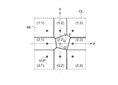
図4は、実施形態1に係るマイクロレンズアレイの平面構成を説明する図である。図5は、マイクロレンズアレイの原理を説明する平面図で、(a)は比較例に係わる1セルの平面構成を示し、(b)は実施形態1に係わるマイクロレンズアレイの1セルの平面構成の一例を示している。次に、実施形態1に係るマイクロレンズアレイ10の構成について、図4及び図5を参照して説明する。尚、図5(a)は従来技術に対応する比較例を説明する図であるが、説明を分かり易くする為に、本実施形態のマイクロレンズアレイ10と共通する要素や名称、符番は同じ物を使用している。
"Microlens array"
FIG. 4 is a diagram illustrating a planar configuration of the microlens array according to the first embodiment. 5A and 5B are plan views for explaining the principle of the microlens array. FIG. 5A is a plan configuration of one cell according to the comparative example, and FIG. 5B is a plan configuration of one cell of the microlens array according to the first embodiment. An example is shown. Next, the configuration of the
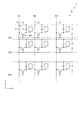
図4に示す様に、マイクロレンズアレイ10は複数個のセルCLを有し、これらのセルCLはX方向及びY方向に行列状に配置されている。マイクロレンズアレイ10を電気光学装置に適応した際には、マイクロレンズアレイ10の一つのセルCLと電気光学装置の一つの画素Pとが、平面視にてアライメントされる。要するに、マイクロレンズアレイ10を構成する一つのセルCLのサイズとその平面視での位置とは、電気光学装置の一つの画素Pのサイズとその平面視での位置とに、設計概念上は一致している。即ち、製造誤差を除いて、セルCLのサイズとその平面視での位置とは、画素Pのサイズとその平面視での位置とに一致している。尚、図4では一例として2セルCL分の平面図を主として描き、マイクロレンズアレイ10を液晶装置1に適応した際に、図4のB−B’線に沿った断面図が図3のB−B’に描かれている。
As shown in FIG. 4, the
各セルCLにはP個(Pは4以上の整数、)のマイクロレンズMLが配置されている。本実施形態ではP=9で、9個のマイクロレンズMLはセルCL内で3行3列に配列されている。一例として、図4の左側のセルCLには(1,1)、(1,2)、(1,3)、(2,1)、(2,2)、(2,3)、(3,1)、(3,2)、(3,3)の9個のマイクロレンズMLが配置され、図4の右側のセルCLには(1,4)、(1,5)、(1,6)、(2,4)、(2,5)、(2,6)、(3,4)、(3,5)、(3,6)の9個のマイクロレンズMLが配置されている。 In each cell CL, P (P is an integer of 4 or more) microlenses ML are arranged. In this embodiment, P = 9, and nine microlenses ML are arranged in three rows and three columns in the cell CL. As an example, the left cell CL in FIG. 4 includes (1,1), (1,2), (1,3), (2,1), (2,2), (2,3), (3 , 1), (3, 2), and (3, 3) are arranged, and the right cell CL in FIG. 4 has (1, 4), (1, 5), (1, Nine microlenses ML of 6), (2, 4), (2, 5), (2, 6), (3,4), (3, 5), (3, 6) are arranged. .
各セルCLにて、P個のマイクロレンズMLの頂点(マイクロレンズピークMLP)は、平面視にて、少なくとも部分的に対称性が破れる様に配置されている。次にマイクロレンズピークMLPの対称性の破れに関して説明する。まず、P個のマイクロレンズMLに対応するP個の格子点を一つのセルCL内に想定する(仮想格子点VLP)。尚、図4等の図面では、マイクロレンズピークMLPの位置を丸印にて示し、仮想格子点VLPの位置を十字印にて示してある。尚、マイクロレンズMLの頂点(マイクロレンズピークMLP)とは、凸レンズではレンズ厚が最も厚い位置であり、凹レンズではレンズ厚が最も薄い位置である。又、凸レンズでレンズ厚が最も厚い領域が平面視にて面状に広がっている平底形状の場合、平底領域の平面視に於ける重心(平底領域の平面視での中心)がマイクロレンズMLの頂点(マイクロレンズピークMLP)である。同様に、凹レンズでレンズ厚が最も薄い領域が平面視にて面状に広がっている平底形状の場合、平底領域の平面視に於ける重心(平底領域の平面視での中心)がマイクロレンズMLの頂点(マイクロレンズピークMLP)である。 In each cell CL, the apexes (microlens peaks MLP) of the P microlenses ML are arranged so that the symmetry is broken at least partially in plan view. Next, the breaking of symmetry of the microlens peak MLP will be described. First, P lattice points corresponding to P microlenses ML are assumed in one cell CL (virtual lattice point VLP). 4 and the like, the position of the microlens peak MLP is indicated by a circle, and the position of the virtual lattice point VLP is indicated by a cross. The apex of the micro lens ML (micro lens peak MLP) is the position where the lens thickness is the thickest in the convex lens and the position where the lens thickness is the thinnest in the concave lens. Further, when the convex lens has a flat bottom shape in which the thickest region of the lens is spread in a planar view, the center of gravity in the plan view of the flat bottom region (the center of the flat bottom region in the plan view) is the microlens ML. It is a vertex (microlens peak MLP). Similarly, in the case of a flat bottom shape in which the region where the lens thickness is the thinnest in a concave lens is spread in a planar shape in plan view, the center of gravity in the plan view of the flat bottom region (center in plan view of the flat bottom region) is the microlens ML. (The microlens peak MLP).
仮想格子点VLPとは、セルCL内にて何らかの形で対称性を保有している点である。例えば、図5(a)(b)に示す様に、セルCLの中心を原点とした直交座標系を考える。図5(a)でも図5(b)でも、仮想格子点VLPはセルCLを均等に分割した交点に設けられている。例えば、図5(b)に示す本実施形態のマイクロレンズアレイ10のセルCLでは、セルCLをX方向にPx等分したPx−1本の線分とY方向にPy等分したPy−1本の線分との交点に(Px−1)×(Py−1)個の仮想格子点VLPが配置されている。本実施形態では、Px=Py=4である。その結果、(Px−1)×(Py−1)個の仮想格子点VLPは、X方向やY方向に関する並進対称性や、原点Oの周りに関する回転対称性、X軸やY軸に関する鏡像反転対称性、等の対称性を保有している。
The virtual lattice point VLP is a point having symmetry in some form in the cell CL. For example, as shown in FIGS. 5A and 5B, consider an orthogonal coordinate system with the center of the cell CL as the origin. In both FIG. 5A and FIG. 5B, the virtual lattice point VLP is provided at the intersection where the cells CL are divided equally. For example, in the cell CL of the
図5(a)に示す比較例では、マイクロレンズピークMLPと仮想格子点VLPとが一致している為に、(Px−1)×(Py−1)個のマイクロレンズピークMLPも、X方向やY方向に関する並進対称性や、原点Oの周りに関する回転対称性、X軸やY軸に関する鏡像反転対称性、等の対称性を保有している。本願発明人が鋭意研究した所に依ると、従来のマイクロレンズMLを用いた電気光学装置で光の利用効率が低かった理由は、以下の様に説明される。即ち、特許文献1に記載されている様なマイクロレンズアレイ10を用いた電気光学装置では、画素内にてレンズ配置が対称性(規則性)を有するので、画素の規則性に起因する回折に加え、画素内レンズの規則性に起因する回折が起こって仕舞う。回折に依る光束の広がりは格子定数(画素サイズやレンズ間距離)に反比例して大きくなる為、一つの画素に一つのレンズが配置された電気光学装置よりも一つの画素に複数個のレンズが規則的に配置された電気光学装置で、より強度の高い回折が生ずる事となる。その結果、回折光の干渉による光の広がり角度がより大きくなる。従来の電気光学装置からの出射光の立体角が大きくなり、投射レンズに入射される割合が減った結果、従来の電気光学装置では明るさが低下していた、と考えられる。
In the comparative example shown in FIG. 5A, since the microlens peak MLP and the virtual lattice point VLP coincide with each other, (Px−1) × (Py−1) microlens peaks MLP are also in the X direction. And translational symmetry in the Y direction, rotational symmetry around the origin O, and mirror image inversion symmetry in the X and Y axes. The reason why the light use efficiency is low in the electro-optical device using the conventional microlens ML is explained as follows, according to the place where the inventor of the present application diligently researched. That is, in the electro-optical device using the
そこで本実施形態のマイクロレンズアレイ10では、図4や図5(b)に示す様に、各セルCLにて、P個(本実施形態では、P=(Px−1)×(Py−1))のマイクロレンズピークMLPの少なくとも1個は、平面視にて、仮想格子点VLPからずれた位置に配置される。その結果、P個のマイクロレンズピークMLPは、平面視にて、少なくとも部分的に対称性が破れる事になる。実際に図5(b)に示すセルCLでは、P個のマイクロレンズピークMLPは一つも仮想格子点VLPに一致しておらず、その結果、P個のマイクロレンズピークMLPは並進対称性も回転対称性も鏡像反転対称性も有していない。要するに、P個のマイクロレンズピークMLPは、平面視にて、並進対称性と回転対称性と鏡像反転対称性とが破れており、セルCL内にて無秩序に配置されている。P個のマイクロレンズピークMLPが、平面視にて、少なくとも部分的にでも対称性が破れていると、画素内のレンズ形状の規則性に起因する回折が抑制されるので、光の利用効率が高いマイクロレンズMLが実現される事になる。更に、P個のマイクロレンズピークMLPがセルCL内にて無秩序に配置されていると、セルCL内のレンズ形状の規則性に起因する回折はより強力に抑制され、更に光の利用効率が高いマイクロレンズMLが実現される事になる。
Therefore, in the
ここで、セルCLに配置された3個のマイクロレンズMLを第1レンズと第2レンズと第3レンズとする。第1レンズと第2レンズとは第一方向(X軸方向)に隣り合って配置された二つのマイクロレンズMLであり、第3レンズは第一方向に直交する第二方向(Y軸方向)に第1レンズと隣り合って配置されたマイクロレンズMLである。本実施形態のマイクロレンズアレイ10では、一つのセルCL内にてP個のマイクロレンズピークMLPは、平面視にて、少なくとも部分的に対称性が破れている為に、第1レンズの頂点と第2レンズの頂点との間隔が、第1レンズの頂点と第3レンズの頂点との間隔と異なる様な3個のマイクロレンズMLがセルCL内に存在する。又、第1レンズの頂点から第2レンズの頂点を結ぶベクトルと、第1レンズの頂点から第3レンズの頂点を結ぶベクトルと、の内積が0と異なる値となる様な3個のマイクロレンズMLがセルCL内に存在する。実際に、図4に示す様に、例えば、(2,2)のマイクロレンズMLを第1レンズ、(2,3)のマイクロレンズMLを第2レンズ、(1,2)のマイクロレンズMLを第3レンズ、とすると、第1レンズの頂点と第2レンズの頂点との間隔は第1レンズの頂点と第3レンズの頂点との間隔と異なっている。更に、第1レンズの頂点から第2レンズの頂点を結ぶベクトルと、第1レンズの頂点から第3レンズの頂点を結ぶベクトルと、の角度が90°と異なる値となっているので、第1レンズの頂点から第2レンズの頂点を結ぶベクトルと、第1レンズの頂点から第3レンズの頂点を結ぶベクトルと、の内積が0と異なる値となっている。
Here, the three microlenses ML arranged in the cell CL are defined as a first lens, a second lens, and a third lens. The first lens and the second lens are two microlenses ML arranged adjacent to each other in the first direction (X-axis direction), and the third lens is a second direction (Y-axis direction) orthogonal to the first direction. The microlens ML is arranged adjacent to the first lens. In the
「表示領域に於けるセル配置」
図6は、実施形態1に係るマイクロレンズアレイの平面的なセル配置を説明する図である。次に、実施形態1に係るマイクロレンズアレイ10のセルCLの配置に関する構成を、図6を参照して、説明する。
"Cell placement in the display area"
FIG. 6 is a diagram illustrating a planar cell arrangement of the microlens array according to the first embodiment. Next, a configuration related to the arrangement of the cells CL of the
セルCLの規則性に起因する回折を抑制するには、セルCLに起因する規則性の周期を波長よりも十分に大きくする事が好ましい。理想的にはセルCLに起因する規則性の周期を光の波長の100倍程度以上とする。斯うすると、セルCLの規則性に起因する回折は著しく抑制される。言い換えると、波長の100倍程度以内の範囲では、マイクロレンズアレイ10を構成するセルCLが皆異なっているのが理想的である。セルCLが異なるとはセルCLを構成するレンズ形状(マイクロレンズピークMLPの配置形状)が其々固有である事を意味する。本実施形態では、光として主に可視光を想定しているので、可視光の干渉を抑制するには、70ミクロン(μm)程度の範囲内で、セルCLは規則性を持たないのが理想的である。一方、電気光学装置では、画素(セルCL)のサイズは7ミクロン(μm)程度と小さい場合もあり得るので、斯うした場合は、10セルCL×10セルCLの単位内ですべてのセルCLが異なっているのが理想的と言える。具体的にはnの二乗個(n2個)のセルCLを単位セル群UGとして、単位セル群UGでnの二乗個(n2個)のセルCLは皆異なっている(nの二乗個(n2個)のセルCLでレンズ形状が皆異なっている)。そしてこの単位セル群UGを繰り返す事で、マイクロレンズアレイ10を構成する。この場合、nは2以上20以下の範囲とし、nを10程度とするのが理想的である。
In order to suppress diffraction due to the regularity of the cell CL, it is preferable that the periodicity due to the cell CL is sufficiently larger than the wavelength. Ideally, the regularity period resulting from the cell CL is set to about 100 times or more of the wavelength of light. In this case, diffraction due to the regularity of the cell CL is remarkably suppressed. In other words, it is ideal that the cells CL constituting the
nを10とすると、100種類の異なったセルCLを形成せねばならないが、これは容易ではない。そこで本実施形態では、図6に示す様に、セルレンズパターンCLP1からセルレンズパターンCLP9まで、9種類の異なったセルCLを構成し、これら9種類のセルCLを単位セル群UGとして、X方向及びY方向に繰り返してマイクロレンズアレイ10としている。セルレンズパターンCLP1やセルレンズパターンCLP2の一例は図4の中央に描かれた2つのセルCLである。図6では、6行9列の54個のセルCLが一例として示され、6個の単位セル群UGが認められる。斯うする事でセルCLの規則性に起因する回折が抑制され、更に光の利用効率は向上する。
If n is 10, it is necessary to form 100 different types of cells CL, but this is not easy. Therefore, in this embodiment, as shown in FIG. 6, nine different cells CL are configured from the cell lens pattern CLP1 to the cell lens pattern CLP9, and these nine types of cells CL are used as a unit cell group UG in the X direction. The
「電気光学装置の製造方法」
図7は、実施形態1に係るマイクロレンズアレイの製造方法を示す概略断面図である。次に、実施形態1に係るマイクロレンズアレイ10を有する液晶装置1の製造方法を、図7を参照して、説明する。尚、図7は、マイクロレンズアレイ10が完成した際に、図4のB−B’線に沿った断面図に相当する。又、図示しないが、マイクロレンズアレイ10の製造工程では、マイクロレンズアレイ10を複数枚取る事ができる大型の基板(マザー基板)で加工が行われ、最終的にそのマザー基板を切断して個片化する事に依り、複数のマイクロレンズアレイ10が得られる。従って、以下に説明する各工程では個片化する前のマザー基板の状態で加工が行われるが、ここでは、マザー基板の中の個別のマイクロレンズアレイ10に対する加工について説明する。
"Method of manufacturing electro-optical device"
FIG. 7 is a schematic cross-sectional view illustrating the method for manufacturing the microlens array according to the first embodiment. Next, a manufacturing method of the
まず、基板上に第一透光性材11を形成する工程を行う。本実施形態では、石英基板が第一透光性材11を兼用しているので、この工程は石英基板を準備する工程となる。
First, the process of forming the 1st
次に、第一透光性材11上にマスク層60を形成する工程を進める。マスク層60は、図7(a)に示す様に、第一透光性材11上の単位領域UAにP個(Pは4以上の整数)の開口部61を有しており、P個の開口部61は、平面視にて、少なくとも部分的に対称性が破れる様に配置されている。単位領域UAはマイクロレンズアレイ10が完成した際にはセルCLとなる領域である。又、開口部61はマイクロレンズアレイ10が完成した際にマイクロレンズピークMLPと平面視で一致する部位である。即ち、開口部61の(X、Y)座標はマイクロレンズピークMLPの(X、Y)座標にほぼ一致している。尚、図7(a)は、一例として図4のB−B’線に沿った部分の断面図を示しているが、説明を分かり易くする為に、B−B’線上に載らない開口部61b(例えば、図4の(1,1)のマイクロレンズMLや(1,4)のマイクロレンズML、(1,5)のマイクロレンズMLを製造する為の開口部61b)も描いてある。又、B−B’線上に載る開口部61a(例えば、図4の(1,2)のマイクロレンズMLや(1,3)のマイクロレンズML、(1,6)のマイクロレンズMLを製造する為の開口部61a)は白抜きで描いてある。更に、図7には仮想格子点VLPも十字印にて示してある。
Next, the process of forming the
P個の開口部61は、平面視にて、少なくとも部分的に対称性が破れる様に配置されている。即ち、P個の開口部61の少なくとも1個は、平面視にて、仮想格子点VLPからずれた位置に配置される。本実施形態が示す様に、P個の開口部61は、単位領域UA内にて無秩序に配置されているのが好ましい。又、単位領域UAに形成される適当な3個の開口部61を第1開口部と第2開口部と第3開口部とする。第1開口部と第2開口部とは第一方向(X軸方向)にほぼ沿いつつ隣り合って配置された二つの開口部61であり、第3開口部は第一方向に直交する第二方向(Y軸方向)にほぼ沿いつつ第1開口部と隣り合って配置された開口部61である。本実施形態では、一つの単位領域UA内にてP個の開口部61は、平面視にて、少なくとも部分的に対称性が破れている為に、第1開口部の平面視での中心位置と第2開口部の平面視での中心位置との間隔が、第1開口部の平面視での中心位置と第3開口部の平面視での中心位置との間隔と異なる様な3個の開口部61が単位領域UA内に存在する。又、第1開口部の平面視での中心位置から第2開口部の平面視での中心位置を結ぶベクトルと、第1開口部の平面視での中心位置から第3開口部の平面視での中心位置を結ぶベクトルと、の内積が0と異なる値となる様な3個の開口部61が単位領域UA内に存在する。例えば、図4の(2,2)のマイクロレンズMLを製造する為の開口部61を第1開口部、(2,3)のマイクロレンズMLを製造する為の開口部61を第2開口部、(1,2)のマイクロレンズMLを製造する為の開口部61を第3開口部、とすると、第1開口部の中心位置と第2開口部の中心位置との間隔は第1開口部の中心位置と第3開口部の中心位置との間隔と異なっている。更に、第1開口部の中心位置から第2開口部の中心位置を結ぶベクトルと、第1開口部の中心位置から第3開口部の中心位置を結ぶベクトルと、の角度が90°と異なる値となっているので、第1開口部の中心位置から第2開口部の中心位置を結ぶベクトルと、第1開口部の中心位置から第3開口部の中心位置を結ぶベクトルと、の内積が0と異なる値となっている。
The
この様なマスク層60は第一透光性材11の上面に、例えば、多結晶シリコン等で形成される。マスク層6となる多結晶シリコンは、例えば、化学気相堆積法(CVD:Chemical Vapor Deposition)や物理気相堆積法(例えば、スパッタリング法等)等で堆積される。堆積された薄膜にはフォトリソグラフィー法とドライエッチング処理とが施されて、開口部61を有するマスク層60が形成される。
Such a
次に、マスク層60を介して第一透光性材11に等方性エッチングを施す事に依り、第一透光性材11に凹部を形成する工程を進める。即ち、マスク層60を介して第一透光性材11に、例えばフッ化水素酸水溶液等のエッチング液を用いた、ウエットエッチング等の等方性エッチング処理を施す。このエッチング処理により、第一透光性材11が上面側から開口部61を中心として等方的にエッチングされる。この結果、図7(a)に示す様に、第一透光性材11に、開口部61に対応して凹部13が形成される。このエッチング処理に依り、凹部13は半球状に形成され、平面視では開口部61を中心として同心円状となる。開口部61からの平面方向(X方向及びY方向)へのエッチング量と深さ方向(Z方向)へのエッチング量とは、ほぼ同程度である。尚、各開口部61からの厚さ方向(Z方向)のエッチング量は総て略同一であるが、図7にはB−B’線における断面形状が描かれているので、B−B’線上に載らない開口部61bからのエッチング深さは、B−B’線上に載る開口部61aからのエッチング深さよりも浅く描かれている。
Next, a process of forming a recess in the first
エッチング処理が終了した後、第一透光性材11からマスク層60を除去し、凹部を第一透光性材11の屈折率とは異なる屈折率を有する第二透光性材12にて埋め込む工程を進める。即ち、第一透光性材11の全領域を覆い凹部13を埋め込む様に、光透過性を有し、第一透光性材11よりも高い屈折率を有する無機材料からなる第二透光性材12を成膜する。第二透光性材12は、例えばCVD法を用いて形成する事ができる。第二透光性材12は第一透光性材11の上面に堆積する様に形成される為、第二透光性材12の表面は第一透光性材11の凹部13及びに起因する凹凸が反映された凹凸形状となる。そこで、第二透光性材12を堆積した後に、この膜に対して平坦化処理を施す。平坦化処理では、例えば、CMP(Chemical Mechanical Polishing)処理等を用いて、第二透光性材12の上層の凹凸が形成された部分を研磨して除去する事により、第二透光性材12の上面が平坦化される。第二透光性材12に平坦化処理を施した結果、図7(b)に示す様に、第二透光性材12の上面が平坦化されて、マイクロレンズアレイ10が完成する。
After the etching process is completed, the
以降の工程は、詳細な図示を省略し、図3を参照して説明する。次に、公知の技術を用いて、マイクロレンズアレイ10上に、光路長調整層31と、遮光層32と、保護層33と、共通電極34と、配向膜35とを順に形成して対向基板30を得る。また、基板21上に、遮光層22と、絶縁層23と、TFT24と、絶縁層25と、遮光層26と、絶縁層27と、画素電極28と、配向膜29とを順に形成して素子基板20を得る。
Subsequent steps will be described with reference to FIG. Next, an optical path
次に、素子基板20と対向基板30との間に、熱硬化性又は光硬化性の接着剤をシール材42(図1参照)として配置して硬化させる。これにより、素子基板20と対向基板30とが接合されて、液晶装置1が完成する。
Next, between the
「電子機器」
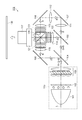
次に、電子機器について図8を参照して説明する。図8は、実施形態1に係る電子機器としてのプロジェクターの構成を示す概略図である。
"Electronics"
Next, an electronic device will be described with reference to FIG. FIG. 8 is a schematic diagram illustrating a configuration of a projector as the electronic apparatus according to the first embodiment.
図8に示す様に、実施形態1に係る電子機器としてのプロジェクター(投射型表示装置)100は、偏光照明装置110と、2つのダイクロイックミラー104,105と、3つの反射ミラー106,107,108と、5つのリレーレンズ111,112,113,114,115と、3つの液晶ライトバルブ121,122,123と、クロスダイクロイックプリズム116と、投射レンズ117とを備えている。
As shown in FIG. 8, a projector (projection display device) 100 as an electronic apparatus according to the first embodiment includes a
偏光照明装置110は、例えば超高圧水銀灯やハロゲンランプ等の白色光源からなる光源としてのランプユニット101と、インテグレーターレンズ102と、偏光変換素子103とを備えている。ランプユニット101と、インテグレーターレンズ102と、偏光変換素子103とは、システム光軸Lに沿って配置されている。
The
ダイクロイックミラー104は、偏光照明装置110から出射された偏光光束のうち、赤色光(R)を反射させ、緑色光(G)と青色光(B)とを透過させる。もう1つのダイクロイックミラー105は、ダイクロイックミラー104を透過した緑色光(G)を反射させ、青色光(B)を透過させる。
The
ダイクロイックミラー104で反射した赤色光(R)は、反射ミラー106で反射した後にリレーレンズ115を経由して液晶ライトバルブ121に入射する。ダイクロイックミラー105で反射した緑色光(G)は、リレーレンズ114を経由して液晶ライトバルブ122に入射する。ダイクロイックミラー105を透過した青色光(B)は、3つのリレーレンズ111,112,113と2つの反射ミラー107,108とで構成される導光系を経由して液晶ライトバルブ123に入射する。
The red light (R) reflected by the
光変調素子としての透過型の液晶ライトバルブ121,122,123は、クロスダイクロイックプリズム116の色光ごとの入射面に対して其々対向配置されている。液晶ライトバルブ121,122,123に入射した色光は、映像情報(映像信号)に基づいて変調され、クロスダイクロイックプリズム116に向けて出射される。
The transmissive liquid crystal
クロスダイクロイックプリズム116は、4つの直角プリズムが貼り合わされて構成されており、その内面には赤色光を反射する誘電体多層膜と青色光を反射する誘電体多層膜とが十字状に形成されている。これらの誘電体多層膜に依って3つの色光が合成されて、カラー画像を表す光が合成される。合成された光は、投射光学系である投射レンズ117に依ってスクリーン130上に投射され、画像が拡大されて表示される。
The cross
液晶ライトバルブ121は、上述した液晶装置1が適用されたものである。液晶ライトバルブ121は、色光の入射側と出射側とに於いてクロスニコルに配置された一対の偏光素子の間に隙間を置いて配置されている。他の液晶ライトバルブ122,123も同様である。
The liquid crystal
実施形態1に係るプロジェクター100の構成によれば、複数の画素Pが高精細に配置されていても、入射した色光を効率よく利用可能でマイクロレンズMLや画素Pに起因する回折光の干渉による光の広がり角度がより小さく抑えられた液晶装置1を備えているので、品質が高く明るいプロジェクター100を提供する事ができる。
According to the configuration of the
本発明は上述した実施形態に限定されず、上述した実施形態に種々の変更や改良などを加えることが可能である。変形例を以下に説明する。 The present invention is not limited to the above-described embodiment, and various modifications and improvements can be added to the above-described embodiment. A modification will be described below.
(変形例1)
「局所的に対称性が破れた形態」
図9は、変形例1に係わるマイクロレンズアレイのセルの一例を説明した図である。次に、図9を参照して変形例1に係わるマイクロレンズアレイ10を説明する。尚、実施形態1と同一の構成部位については、同一の符号を附し、重複する説明は省略する。
(Modification 1)
"Locally broken symmetry"
FIG. 9 is a diagram illustrating an example of a microlens array cell according to the first modification. Next, a
図9に示す本変形例のマイクロレンズアレイ10では、セルCLを構成するマイクロレンズMLの形状が異なっている。それ以外は実施形態1と同様である。図5(b)に示す実施形態1では、セルCL内でマイクロレンズML形状の対称性は完全に破られ、マイクロレンズピークMLPは無秩序に配置されていたが、本変形例が示す様に、マイクロレンズML形状は部分的に対称性が破れていても良い。例えば、図9に示す様に、P個のマイクロレンズMLの内で少なくとも一つのマイクロレンズMLで対称性が破れていても、マイクロレンズMLの規則性に起因する回折は抑制される。図9では(2,2)のマイクロレンズMLが対称性を破っている。即ち、(2,2)のマイクロレンズMLのマイクロレンズピークMLPは仮想格子点VLPからずれている。この結果、並進対称性も回転対称性も鏡像反転対称性も部分的に破れており、この破れに応ずる分だけ、マイクロレンズMLの規則性に起因する回折は抑制される。
In the
(変形例2)
「仮想格子点が異なる形態」
図10は、変形例2に係わるマイクロレンズアレイのセルの一例を説明した図である。次に、図10を参照して変形例2に係わるマイクロレンズアレイ10を説明する。尚、実施形態1と同一の構成部位については、同一の符号を附し、重複する説明は省略する。
(Modification 2)
"Forms with different virtual grid points"
FIG. 10 is a diagram illustrating an example of a microlens array cell according to the second modification. Next, a
図10に示す本変形例のマイクロレンズアレイ10では、セルCLを構成するマイクロレンズMLの仮想格子点VLPが異なっている。それ以外は実施形態1と同様である。図5(b)に示す実施形態1では、仮想格子点VLPはセルCLを均等に分割した交点に設けられていた。仮想格子点VLPはこれに限られず、何らかの対称性を有していれば、如何なる配置であっても構わない。図10では、仮想格子点VLPがセルCLの中央に集められており、並進対称性と回転対称性、鏡像反転対称性とを有している。この仮想格子点VLPに対して、マイクロレンズピークMLPをずらして、マイクロレンズMLの配置を無秩序としても良い。
In the
(変形例3)
「単位セル群が異なる形態」
図11は、変形例3に係わるマイクロレンズアレイの一例を説明した図である。次に、図11を参照して変形例3に係わるマイクロレンズアレイ10を説明する。尚、実施形態1と同一の構成部位については、同一の符号を附し、重複する説明は省略する。
(Modification 3)
"Forms with different unit cell groups"
FIG. 11 is a diagram illustrating an example of a microlens array according to the third modification. Next, a
図11に示す本変形例のマイクロレンズアレイ10では、マイクロレンズアレイ10を構成する単位セル群UGが異なっている。それ以外は実施形態1と同様である。図6に示された実施形態1のマイクロレンズアレイ10では単位セル群UGは9個の異なったセルCLで構成され、この単位セル群UGを繰り返されていた。単位セル群UGの構成はこれに限られず、様々形態が可能である。図11に示す様に、単位セル群UGはn二乗個の異なったセルCLを含むが、単位セル群UGの中でこれらのセルCLの配置を変えても良い。本変形例では、複数種類の単位セル群UGを準備し、各単位セル群UGでセルCLの配置をかえる。例えば、図11に示す様に、セルレンズパターンCLP1からセルレンズパターンCLP4まで、4種類の異なったセルCLを準備し、これら4種類のセルCLの配置を変えた複数種類の単位セル群UGを作る。図11の例では第1単位セル群UGから第9単位セル群UG迄9種類の単位セル群UGが作られ、各単位セル群UGの中で4種類の異なったセルCLの配置が変えられている。この様に複数種類の単位セル群UGを用いてマイクロレンズアレイ10を構成しても良い。
In the
CL…セル、CLP…セルレンズパターン、E…表示領域、ML…マイクロレンズ、MLP…マイクロレンズピーク、O…原点、P…画素、UA…単位領域、UG…単位セル群、VLP…仮想格子点、1…液晶装置、2…走査線、3…データ線、4…容量線、5…蓄積容量、6…マスク層、10…マイクロレンズアレイ、11…第一透光性材、12…第二透光性材、13…凹部、20…素子基板、21…基板、22…遮光層、22a…遮光層、23…絶縁層、24…TFT、25…絶縁層、26…遮光層、26a…遮光層、27…絶縁層、28…画素電極、29…配向膜、30…対向基板、31…光路長調整層、32…遮光層、33…保護層、34…共通電極、35…配向膜、40…液晶、42…シール材、51…データ線駆動回路、52…走査線駆動回路、53…検査回路、54…外部接続端子、55…配線、56…上下導通部、60…マスク層、61…開口部、61a…開口部、61b…開口部、100…プロジェクター、101…ランプユニット、102…インテグレーターレンズ、103…偏光変換素子、104…ダイクロイックミラー、105…ダイクロイックミラー、106…反射ミラー、107…反射ミラー、108…反射ミラー、110…偏光照明装置、111…リレーレンズ、112…リレーレンズ、113…リレーレンズ、114…リレーレンズ、115…リレーレンズ、116…クロスダイクロイックプリズム、117…投射レンズ、121…液晶ライトバルブ、122…液晶ライトバルブ、123…液晶ライトバルブ、130…スクリーン。
CL: Cell, CLP: Cell lens pattern, E: Display area, ML: Micro lens, MLP: Micro lens peak, O: Origin, P: Pixel, UA: Unit area, UG: Unit cell group, VLP: Virtual lattice point DESCRIPTION OF
Claims (11)
前記第1レンズと前記第2レンズとは第一方向に隣り合って配置され、
前記第1レンズと前記第3レンズとは前記第一方向に略直交する第二方向に隣り合って配置され、
前記第1レンズの頂点と前記第2レンズの頂点との間隔は、前記第1レンズの頂点と前記第3レンズの頂点との間隔と異なる事を特徴とするマイクロレンズアレイ。 Including a first lens, a second lens, and a third lens disposed in the cell;
The first lens and the second lens are arranged adjacent to each other in the first direction,
The first lens and the third lens are arranged adjacent to each other in a second direction substantially orthogonal to the first direction,
The microlens array, wherein an interval between the apex of the first lens and the apex of the second lens is different from an interval between the apex of the first lens and the apex of the third lens.
前記第1レンズと前記第2レンズとは第一方向に隣り合って配置され、
前記第1レンズと前記第3レンズとは前記第一方向に略直交する第二方向に隣り合って配置され、
前記第1レンズの頂点から前記第2レンズの頂点を結ぶベクトルと、前記第1レンズの頂点から前記第3レンズの頂点を結ぶベクトルと、の内積が0と異なる値である事を特徴とするマイクロレンズアレイ。 Including a first lens, a second lens, and a third lens disposed in the cell;
The first lens and the second lens are arranged adjacent to each other in the first direction,
The first lens and the third lens are arranged adjacent to each other in a second direction substantially orthogonal to the first direction,
An inner product of a vector connecting the vertex of the first lens and the vertex of the second lens and a vector connecting the vertex of the first lens and the vertex of the third lens is a value different from 0. Micro lens array.
前記P個のレンズの頂点は、平面視にて、少なくとも部分的に対称性が破れる様に配置されている事を特徴とするマイクロレンズアレイ。 Including P lenses (P is an integer of 4 or more) arranged in the cell,
The apex of the P lenses is arranged so that symmetry is broken at least partially in a plan view.
前記第一透光性材上に第1開口部と第2開口部と第3開口部とを有するマスク層を形成する工程と、
前記マスク層を介して前記第一透光性材に等方性エッチングを施す事に依り、前記第一透光性材に凹部を形成する工程と、
前記凹部を前記第一透光性材の屈折率とは異なる屈折率を有する第二透光性材にて埋め込む工程と、を含み、
前記第1開口部と前記第2開口部とは第一方向に隣り合って配置され、
前記第1開口部と前記第3開口部とは前記第一方向に略直交する第二方向に隣り合って配置され、
前記第1開口部の中心位置と前記第2開口部の中心位置との間隔は、前記第1開口部の中心位置と前記第3開口部の中心位置との間隔と異なる事を特徴とするマイクロレンズアレイの製造方法。 Forming a first translucent material on the substrate;
Forming a mask layer having a first opening, a second opening, and a third opening on the first translucent material;
Forming a recess in the first light transmissive material by performing isotropic etching on the first light transmissive material through the mask layer;
Embedding the recess with a second light transmissive material having a refractive index different from the refractive index of the first light transmissive material,
The first opening and the second opening are arranged adjacent to each other in the first direction,
The first opening and the third opening are arranged adjacent to each other in a second direction substantially orthogonal to the first direction,
The distance between the center position of the first opening and the center position of the second opening is different from the distance between the center position of the first opening and the center position of the third opening. A method of manufacturing a lens array.
前記第一透光性材上に第1開口部と第2開口部と第3開口部とを有するマスク層を形成する工程と、
前記マスク層を介して前記第一透光性材に等方性エッチングを施す事に依り、前記第一透光性材に凹部を形成する工程と、
前記凹部を前記第一透光性材の屈折率とは異なる屈折率を有する第二透光性材にて埋め込む工程と、を含み、
前記第1開口部と前記第2開口部とは第一方向に隣り合って配置され、
前記第1開口部と前記第3開口部とは前記第一方向に略直交する第二方向に隣り合って配置され、
前記第1開口部の中心位置から前記第2開口部の中心位置を結ぶベクトルと、前記第1開口部の中心位置から前記第3開口部の中心位置を結ぶベクトルと、の内積が0と異なる値である事を特徴とするマイクロレンズアレイの製造方法。 Forming a first translucent material on the substrate;
Forming a mask layer having a first opening, a second opening, and a third opening on the first translucent material;
Forming a recess in the first light transmissive material by performing isotropic etching on the first light transmissive material through the mask layer;
Embedding the recess with a second light transmissive material having a refractive index different from the refractive index of the first light transmissive material,
The first opening and the second opening are arranged adjacent to each other in the first direction,
The first opening and the third opening are arranged adjacent to each other in a second direction substantially orthogonal to the first direction,
The inner product of a vector connecting the center position of the first opening to the center position of the second opening and a vector connecting the center position of the first opening to the center position of the third opening is different from zero. A manufacturing method of a microlens array characterized by being a value.
前記第一透光性材上の単位領域にP個(Pは4以上の整数)の開口部を有するマスク層を形成する工程と、
前記マスク層を介して前記第一透光性材に等方性エッチングを施す事に依り、前記第一透光性材に凹部を形成する工程と、
前記凹部を前記第一透光性材の屈折率とは異なる屈折率を有する第二透光性材にて埋め込む工程と、を含み、
前記P個の開口部は、平面視にて、少なくとも部分的に対称性が破れる様に配置されている事を特徴とするマイクロレンズアレイの製造方法。 Forming a first translucent material on the substrate;
Forming a mask layer having P (P is an integer of 4 or more) openings in a unit region on the first translucent material;
Forming a recess in the first light transmissive material by performing isotropic etching on the first light transmissive material through the mask layer;
Embedding the recess with a second light transmissive material having a refractive index different from the refractive index of the first light transmissive material,
The method for manufacturing a microlens array, wherein the P openings are arranged so that symmetry is broken at least partially in a plan view.
Priority Applications (3)
| Application Number | Priority Date | Filing Date | Title |
|---|---|---|---|
| JP2014002194A JP2015129894A (en) | 2014-01-09 | 2014-01-09 | Microlens array, method for manufacturing microlens array, electro-optic device, and electronic apparatus |
| US14/569,702 US9477015B2 (en) | 2014-01-09 | 2014-12-13 | Microlens array, method for manufacturing microlens array, electro-optical device and electronic apparatus |
| US15/284,258 US10007033B2 (en) | 2014-01-09 | 2016-10-03 | Microlens array, method for manufacturing microlens array, electro-optical device and electronic apparatus |
Applications Claiming Priority (1)
| Application Number | Priority Date | Filing Date | Title |
|---|---|---|---|
| JP2014002194A JP2015129894A (en) | 2014-01-09 | 2014-01-09 | Microlens array, method for manufacturing microlens array, electro-optic device, and electronic apparatus |
Publications (2)
| Publication Number | Publication Date |
|---|---|
| JP2015129894A true JP2015129894A (en) | 2015-07-16 |
| JP2015129894A5 JP2015129894A5 (en) | 2017-01-19 |
Family
ID=53495009
Family Applications (1)
| Application Number | Title | Priority Date | Filing Date |
|---|---|---|---|
| JP2014002194A Withdrawn JP2015129894A (en) | 2014-01-09 | 2014-01-09 | Microlens array, method for manufacturing microlens array, electro-optic device, and electronic apparatus |
Country Status (2)
| Country | Link |
|---|---|
| US (2) | US9477015B2 (en) |
| JP (1) | JP2015129894A (en) |
Cited By (2)
| Publication number | Priority date | Publication date | Assignee | Title |
|---|---|---|---|---|
| JP2021076875A (en) * | 2019-11-06 | 2021-05-20 | デクセリアルズ株式会社 | Microlens array and projection image display device |
| US11960103B2 (en) | 2019-11-06 | 2024-04-16 | Dexerials Corporation | Micro-lens array, projection type image display device, method for designing micro-lens array, and method for manufacturing micro-lens array |
Families Citing this family (5)
| Publication number | Priority date | Publication date | Assignee | Title |
|---|---|---|---|---|
| JP2015129894A (en) * | 2014-01-09 | 2015-07-16 | セイコーエプソン株式会社 | Microlens array, method for manufacturing microlens array, electro-optic device, and electronic apparatus |
| US11138706B2 (en) * | 2018-01-26 | 2021-10-05 | Aerovironment, Inc. | Voronoi cropping of images for post field generation |
| CN108445558B (en) * | 2018-03-27 | 2021-01-26 | 京东方科技集团股份有限公司 | Optical film material structure, forming method thereof and display device |
| FR3102007B1 (en) * | 2019-10-14 | 2021-10-29 | Commissariat Energie Atomique | Image sensor |
| JP2022141058A (en) * | 2021-03-15 | 2022-09-29 | オムロン株式会社 | Display switching device |
Citations (10)
| Publication number | Priority date | Publication date | Assignee | Title |
|---|---|---|---|---|
| JPH08248403A (en) * | 1995-03-14 | 1996-09-27 | Kuraray Co Ltd | Liquid crystal display device |
| JP2001215485A (en) * | 2000-01-31 | 2001-08-10 | Toppan Printing Co Ltd | Reflection type liquid crystal display device |
| JP2004505306A (en) * | 2000-07-31 | 2004-02-19 | ロチェスター フォトニクス コーポレイション | Structured screen for controlled light dispersion |
| JP2004287372A (en) * | 2003-01-28 | 2004-10-14 | Seiko Epson Corp | Method for manufacturing base plate with recessed part, base plate with recessed part, base plate with recessed part for microlens, microlens base plate, transmission type screen and rear type projector |
| JP2005070639A (en) * | 2003-08-27 | 2005-03-17 | Fuji Photo Film Co Ltd | Viewing angle adjustment filter and display device |
| JP2006251659A (en) * | 2005-03-14 | 2006-09-21 | Fuji Photo Film Co Ltd | Viewing angle expansion film and display device using the viewing angle expansion film |
| JP2006284831A (en) * | 2005-03-31 | 2006-10-19 | Sanyo Epson Imaging Devices Corp | Electrooptical apparatus and electronic device |
| US20080117519A1 (en) * | 2006-11-17 | 2008-05-22 | Eastman Kodak Company | Light emitting device with microlens array |
| JP2011158755A (en) * | 2010-02-02 | 2011-08-18 | Sony Corp | Liquid crystal display element and projection type liquid crystal display device equipped with liquid crystal display element |
| JP2013076881A (en) * | 2011-09-30 | 2013-04-25 | Dainippon Printing Co Ltd | Optical sheet and image display unit |
Family Cites Families (13)
| Publication number | Priority date | Publication date | Assignee | Title |
|---|---|---|---|---|
| US4496216A (en) * | 1982-12-30 | 1985-01-29 | Polaroid Corporation | Method and apparatus for exposing photosensitive material |
| JP3251150B2 (en) * | 1994-12-29 | 2002-01-28 | 日本板硝子株式会社 | Flat microlens array and method of manufacturing the same |
| JP2001075091A (en) | 1999-07-07 | 2001-03-23 | Matsushita Electric Ind Co Ltd | Semitransmitting liquid crystal display device |
| WO2001004695A1 (en) | 1999-07-07 | 2001-01-18 | Matsushita Electric Industrial Co., Ltd. | Translucent liquid crystal display device |
| US6800877B2 (en) | 2000-05-26 | 2004-10-05 | Exaconnect Corp. | Semi-conductor interconnect using free space electron switch |
| US6835535B2 (en) | 2000-07-31 | 2004-12-28 | Corning Incorporated | Microlens arrays having high focusing efficiency |
| JP4845290B2 (en) * | 2001-06-20 | 2011-12-28 | キヤノン株式会社 | Micro lens array, optical equipment and optical viewfinder |
| JP4495917B2 (en) | 2003-04-03 | 2010-07-07 | 株式会社リコー | Image display device |
| JP2005352392A (en) | 2004-06-14 | 2005-12-22 | Ricoh Co Ltd | Microlens array, spatial optical modulation device, and projector apparatus |
| JP4618446B2 (en) * | 2004-06-23 | 2011-01-26 | 株式会社ニコン | Optical element, optical system and waveguide |
| DE102007050167A1 (en) * | 2007-10-19 | 2009-04-23 | Fraunhofer-Gesellschaft zur Förderung der angewandten Forschung e.V. | Microlens array with integrated illumination |
| CN103365021B (en) * | 2012-04-03 | 2015-11-25 | 元太科技工业股份有限公司 | Electrophoretic display device capable of switching between color mode and black-and-white mode |
| JP2015129894A (en) * | 2014-01-09 | 2015-07-16 | セイコーエプソン株式会社 | Microlens array, method for manufacturing microlens array, electro-optic device, and electronic apparatus |
-
2014
- 2014-01-09 JP JP2014002194A patent/JP2015129894A/en not_active Withdrawn
- 2014-12-13 US US14/569,702 patent/US9477015B2/en active Active
-
2016
- 2016-10-03 US US15/284,258 patent/US10007033B2/en active Active
Patent Citations (10)
| Publication number | Priority date | Publication date | Assignee | Title |
|---|---|---|---|---|
| JPH08248403A (en) * | 1995-03-14 | 1996-09-27 | Kuraray Co Ltd | Liquid crystal display device |
| JP2001215485A (en) * | 2000-01-31 | 2001-08-10 | Toppan Printing Co Ltd | Reflection type liquid crystal display device |
| JP2004505306A (en) * | 2000-07-31 | 2004-02-19 | ロチェスター フォトニクス コーポレイション | Structured screen for controlled light dispersion |
| JP2004287372A (en) * | 2003-01-28 | 2004-10-14 | Seiko Epson Corp | Method for manufacturing base plate with recessed part, base plate with recessed part, base plate with recessed part for microlens, microlens base plate, transmission type screen and rear type projector |
| JP2005070639A (en) * | 2003-08-27 | 2005-03-17 | Fuji Photo Film Co Ltd | Viewing angle adjustment filter and display device |
| JP2006251659A (en) * | 2005-03-14 | 2006-09-21 | Fuji Photo Film Co Ltd | Viewing angle expansion film and display device using the viewing angle expansion film |
| JP2006284831A (en) * | 2005-03-31 | 2006-10-19 | Sanyo Epson Imaging Devices Corp | Electrooptical apparatus and electronic device |
| US20080117519A1 (en) * | 2006-11-17 | 2008-05-22 | Eastman Kodak Company | Light emitting device with microlens array |
| JP2011158755A (en) * | 2010-02-02 | 2011-08-18 | Sony Corp | Liquid crystal display element and projection type liquid crystal display device equipped with liquid crystal display element |
| JP2013076881A (en) * | 2011-09-30 | 2013-04-25 | Dainippon Printing Co Ltd | Optical sheet and image display unit |
Cited By (2)
| Publication number | Priority date | Publication date | Assignee | Title |
|---|---|---|---|---|
| JP2021076875A (en) * | 2019-11-06 | 2021-05-20 | デクセリアルズ株式会社 | Microlens array and projection image display device |
| US11960103B2 (en) | 2019-11-06 | 2024-04-16 | Dexerials Corporation | Micro-lens array, projection type image display device, method for designing micro-lens array, and method for manufacturing micro-lens array |
Also Published As
| Publication number | Publication date |
|---|---|
| US9477015B2 (en) | 2016-10-25 |
| US10007033B2 (en) | 2018-06-26 |
| US20150192705A1 (en) | 2015-07-09 |
| US20170023707A1 (en) | 2017-01-26 |
Similar Documents
| Publication | Publication Date | Title |
|---|---|---|
| JP6221480B2 (en) | Electro-optical device, method of manufacturing electro-optical device, and electronic apparatus | |
| JP6111601B2 (en) | Microlens array substrate, microlens array substrate manufacturing method, electro-optical device, and electronic apparatus | |
| US9354467B2 (en) | Electro-optical device and electronic apparatus | |
| US10007033B2 (en) | Microlens array, method for manufacturing microlens array, electro-optical device and electronic apparatus | |
| JP6123317B2 (en) | Liquid crystal device and electronic device | |
| JP6318881B2 (en) | Microlens array substrate, microlens array substrate manufacturing method, electro-optical device, and electronic apparatus | |
| JP6398164B2 (en) | Microlens array substrate manufacturing method, microlens array substrate, electro-optical device, and electronic apparatus | |
| JP2015138078A (en) | Microlens array, method of manufacturing the microlens array, electro-optical device, and electronic apparatus | |
| JP2016151735A (en) | Lens array substrate, electro-optic device, electronic apparatus, and method for manufacturing lens array substrate | |
| JP2015022100A (en) | Electro-optic device, method for manufacturing electro-optic device, and electronic equipment | |
| JP6111600B2 (en) | Manufacturing method of microlens array substrate | |
| JP6237070B2 (en) | Microlens array substrate, electro-optical device, and electronic device | |
| JP6398361B2 (en) | Microlens array substrate, electro-optical device, and electronic device | |
| JP2016224459A (en) | Microlens array substrate, electro-optical device and electronic apparatus | |
| JP6318946B2 (en) | Microlens array substrate, electro-optical device, and electronic device | |
| JP6414256B2 (en) | Microlens array substrate, microlens array substrate manufacturing method, electro-optical device, and electronic apparatus | |
| JP2015138165A (en) | Microlens array, method of manufacturing the microlens array, electro-optical device, and electronic apparatus | |
| JP2017219700A (en) | Large-sized substrate, liquid crystal device, method of manufacturing large-sized substrate, method of manufacturing liquid crystal device, and electronic apparatus | |
| JP6299493B2 (en) | Microlens array substrate, electro-optical device, and electronic device | |
| JP2015094879A (en) | Manufacturing method for microlens array substrate, electro-optical device, and electronic device | |
| JP2015087571A (en) | Method for manufacturing microlens array substrate, microlens array substrate, electro-optic device, and electronic equipment | |
| JP2015129895A (en) | Microlens array, method for manufacturing microlens array, electro-optic device, and electronic equipment | |
| JP2015203744A (en) | Electro-optic device and electronic equipment | |
| JP2015049412A (en) | Electro-optic device, method for manufacturing electro-optic device, and electronic equipment | |
| JP2015148658A (en) | Microlens array, method for manufacturing microlens array, electro-optic device, and electronic equipment |
Legal Events
| Date | Code | Title | Description |
|---|---|---|---|
| RD04 | Notification of resignation of power of attorney |
Free format text: JAPANESE INTERMEDIATE CODE: A7424 Effective date: 20160617 |
|
| RD03 | Notification of appointment of power of attorney |
Free format text: JAPANESE INTERMEDIATE CODE: A7423 Effective date: 20160624 |
|
| A521 | Request for written amendment filed |
Free format text: JAPANESE INTERMEDIATE CODE: A523 Effective date: 20161206 |
|
| A621 | Written request for application examination |
Free format text: JAPANESE INTERMEDIATE CODE: A621 Effective date: 20161206 |
|
| A977 | Report on retrieval |
Free format text: JAPANESE INTERMEDIATE CODE: A971007 Effective date: 20170823 |
|
| A131 | Notification of reasons for refusal |
Free format text: JAPANESE INTERMEDIATE CODE: A131 Effective date: 20170926 |
|
| RD02 | Notification of acceptance of power of attorney |
Free format text: JAPANESE INTERMEDIATE CODE: A7422 Effective date: 20171118 |
|
| A521 | Request for written amendment filed |
Free format text: JAPANESE INTERMEDIATE CODE: A523 Effective date: 20171121 |
|
| A131 | Notification of reasons for refusal |
Free format text: JAPANESE INTERMEDIATE CODE: A131 Effective date: 20180501 |
|
| A761 | Written withdrawal of application |
Free format text: JAPANESE INTERMEDIATE CODE: A761 Effective date: 20180530 |