JP5122885B2 - Capacitor-embedded wiring board and manufacturing method thereof - Google Patents
Capacitor-embedded wiring board and manufacturing method thereof Download PDFInfo
- Publication number
- JP5122885B2 JP5122885B2 JP2007204187A JP2007204187A JP5122885B2 JP 5122885 B2 JP5122885 B2 JP 5122885B2 JP 2007204187 A JP2007204187 A JP 2007204187A JP 2007204187 A JP2007204187 A JP 2007204187A JP 5122885 B2 JP5122885 B2 JP 5122885B2
- Authority
- JP
- Japan
- Prior art keywords
- layer
- capacitor
- conductor
- hole
- electrode layer
- Prior art date
- Legal status (The legal status is an assumption and is not a legal conclusion. Google has not performed a legal analysis and makes no representation as to the accuracy of the status listed.)
- Expired - Fee Related
Links
Images


Landscapes
- Parts Printed On Printed Circuit Boards (AREA)
- Production Of Multi-Layered Print Wiring Board (AREA)
Description
本発明は、電極層及び誘電体層を備えるコンデンサを内蔵したコンデンサ内蔵配線基板及びその製造方法に関するものである。 The present invention relates to a capacitor built-in wiring board having a capacitor including an electrode layer and a dielectric layer, and a method for manufacturing the same.
近年における電子機器の高性能化や小型化の要求は高く、このような要求が高まるにつれて電子部品の高密度化や高機能化に対する要求も確実に高くなってきている。それゆえ、配線基板における電子部品の実装効率を上げるために、例えば、電子部品(ここではコンデンサ)を内蔵した構造の部品内蔵配線基板などが各種提案されている(例えば特許文献1参照)。 In recent years, there has been a high demand for high performance and miniaturization of electronic devices, and the demand for higher density and higher functionality of electronic components has been steadily increasing as such demands have increased. Therefore, in order to increase the mounting efficiency of electronic components on the wiring board, for example, various types of component-embedded wiring boards with a built-in electronic component (here, a capacitor) have been proposed (see, for example, Patent Document 1).
上記従来の部品内蔵配線基板(コンデンサ内蔵配線基板)の一例を図13に基づいて説明する。コンデンサ内蔵配線基板は、コア基板151上に、複数層の樹脂層間絶縁層152からなるビルドアップ層を形成してなる。樹脂層間絶縁層152内にはコンデンサ153が埋め込まれている。コンデンサ153は、ニッケル箔からなる電極層154を備えている。電極層154は、電極層側貫通孔155を有するとともに、第1主面156上及び第2主面157上にチタン酸バリウムからなる誘電体層158が形成されている。さらに、各誘電体層158上には、ニッケルペースト層を焼結して得た電極層159が形成されている。また、各樹脂層間絶縁層152内には、コンデンサ153を厚さ方向に貫通する貫通ビア導体160が設けられている。貫通ビア導体160の底部はコア基板151上の内層側導体層161に面接触し、貫通ビア導体160の外周部は電極層側貫通孔155の内壁面及び第1主面156側の開口縁に面接触している。
ところが、コンデンサ内蔵配線基板の製造時や使用時に熱応力が作用する場合があるが、そのときの熱応力が大きいと、貫通ビア導体160と電極層154との界面が剥離するおそれがある。従って、この場合には、貫通ビア導体160と電極層154との接続信頼性を確保できなくなる。
However, thermal stress may act during manufacture and use of the capacitor built-in wiring board. If the thermal stress at that time is large, the interface between the through via
また、各樹脂層間絶縁層152のうちコンデンサ153を有する層の厚さがコンデンサ153の厚さ分だけ増加しているため、貫通ビア導体160のアスペクト比(貫通ビア導体160の高さを直径で割った値)が大きい。即ち、貫通ビア導体160の直径が貫通ビア導体160の高さに対して小さい。このことから、貫通ビア導体160の底部と内層側導体層161との接触面積(ビア底面積)が小さくなり、熱応力が作用した際に、貫通ビア導体160の底部と内層側導体層161との界面が剥離しやすい。従って、貫通ビア導体160と内層側導体層161との接続信頼性を確保することが困難である。
In addition, since the thickness of the layer having the
本発明は上記の課題に鑑みてなされたものであり、その目的は、貫通ビア導体と他の導体との間の剥離を防止することにより、信頼性が高くなるコンデンサ内蔵配線基板及びその製造方法を提供することにある。 The present invention has been made in view of the above problems, and an object of the present invention is to provide a wiring board with a built-in capacitor that is highly reliable by preventing peeling between a through via conductor and another conductor, and a method for manufacturing the same. Is to provide.
上記課題を解決するための手段(手段1)としては、第1主面(12,107)及び第2主面(13,108)を有する電極層(11,103)と、前記電極層(11,103)の前記第1主面(12,107)及び前記第2主面(13,108)の少なくともいずれかの上に形成された誘電体層(21,104)とを有するコンデンサ(10,101)が、前記第2主面(13,108)側を内層側に配置しかつ前記第1主面(12,107)側を外層側に配置した状態で、配線基板(71)における配線積層部(73)を構成する樹脂層間絶縁層(81,82,83,84)内に埋め込まれているコンデンサ内蔵配線基板(71)であって、前記コンデンサ(10,101)をその厚さ方向に貫通する貫通ビア導体(121)が、前記樹脂層間絶縁層(81,82)内に設けられ、前記貫通ビア導体(121)の底部が、前記コンデンサ(10,101)よりも内層側に位置する内層側導体層(123)に面接触し、前記貫通ビア導体(121)の外周部が、前記電極層(11,103)に形成された電極層側貫通孔(109,112)の第1主面(12,107)側開口縁、内壁面及び第2主面(13,108)側開口縁に面接触し、前記貫通ビア導体(121)は、前記樹脂層間絶縁層(81,82)を貫通して前記内層側導体層(123)を露出させるビア孔(228)に充填されたフィルドビア導体であって、頂部から底部に行くに従って全体的に外径が徐々に小さくなる形状をなしており、前記貫通ビア導体(121)の頂部及び底部における外径が、前記電極層側貫通孔(109,112)の内径よりも大きく、前記内層側導体層(123)と前記貫通ビア導体(121)の底部との接触部分の直径が、前記電極層側貫通孔(109,112)の内径よりも大きいことを特徴とするコンデンサ内蔵配線基板がある。 Means for solving the above problems (means 1) include an electrode layer (11, 103) having a first main surface (12, 107) and a second main surface (13, 108), and the electrode layer (11 , 103) and a dielectric layer (21, 104) formed on at least one of the first main surface (12, 107) and the second main surface (13, 108). 101) in the state where the second main surface (13, 108) side is arranged on the inner layer side and the first main surface (12, 107) side is arranged on the outer layer side, the wiring lamination on the wiring substrate (71) A capacitor built-in wiring board (71) embedded in a resin interlayer insulating layer (81, 82, 83, 84) constituting the portion (73), wherein the capacitor (10, 101) is disposed in the thickness direction thereof. The through via conductor (121) that penetrates the tree Provided in the interlayer insulating layer (81, 82), the bottom of the through via conductor (121) is in surface contact with the inner layer side conductor layer (123) located on the inner layer side of the capacitor (10, 101), The outer peripheral portion of the through via conductor (121) has an opening edge on the first main surface (12, 107) side of the electrode layer side through hole (109, 112) formed in the electrode layer (11, 103), an inner wall surface And the through via conductor (121) penetrates the resin interlayer insulating layer (81, 82) and the inner layer side conductor layer (123) in surface contact with the opening edge on the second main surface (13, 108) side. A filled via conductor filled in a via hole (228) to be exposed, the outer diameter gradually decreasing from the top to the bottom, and the top and bottom of the through via conductor (121) outer diameter of the said electrode layer side Hole (109, 112) much larger than the inner diameter of the diameter of the contact portion between the bottom of the inside conductor layer (123) and the through via conductors (121), the electrode layer side through holes (109, 112 There is a wiring board with a built-in capacitor characterized in that it is larger than the inner diameter .
従って、この手段1のコンデンサ内蔵配線基板によると、貫通ビア導体が、電極層側貫通孔の第1主面側開口縁及び内壁面に面接触する。それに加えて、貫通ビア導体の外径が電極層側貫通孔の内径よりも大きいために、貫通ビア導体は、電極層の第2主面側に回り込んで第2主面側開口縁にも面接触する。よって、貫通ビア導体と電極層との接触面積が大きくなり、両者の密着強度も大きくなる。ゆえに、熱応力が作用したとしても、貫通ビア導体と電極層との間の剥離を防止できるため、貫通ビア導体と電極層との接続信頼性が高くなる。しかも、貫通ビア導体が、電極層を第1主面側及び第2主面側の両方から挟み込む構造であるため、貫通ビア導体と電極層との接触部分の一部が剥離したとしても、他の部分が接触状態を維持することができる。よって、貫通ビア導体と電極層との接続信頼性がよりいっそう高くなる。また、貫通ビア導体が電極層の第2主面側に回り込む形状であることから、貫通ビア導体の底部の直径が従来よりも大きくなる。よって、貫通ビア導体の底部と内層側導体層との接触面積が大きくなり、両者の密着強度も大きくなる。ゆえに、熱応力が作用したとしても、貫通ビア導体の底部と内層側導体層との剥離を防止できるため、貫通ビア導体と内層側導体層との接続信頼性が高くなる。よって、信頼性が高いコンデンサ内蔵配線基板を実現することができる。 Therefore, according to the capacitor built-in wiring board of the means 1, the through via conductor is in surface contact with the opening edge and the inner wall surface of the first main surface side of the electrode layer side through hole. In addition, since the outer diameter of the through via conductor is larger than the inner diameter of the electrode layer side through hole, the through via conductor wraps around the second main surface side of the electrode layer and also on the second main surface side opening edge. Surface contact. Therefore, the contact area between the through via conductor and the electrode layer is increased, and the adhesion strength between the two is also increased. Therefore, even if a thermal stress is applied, peeling between the through via conductor and the electrode layer can be prevented, so that the connection reliability between the through via conductor and the electrode layer is increased. Moreover, since the through via conductor has a structure in which the electrode layer is sandwiched from both the first main surface side and the second main surface side, even if a part of the contact portion between the through via conductor and the electrode layer is peeled off, This part can maintain the contact state. Therefore, the connection reliability between the through via conductor and the electrode layer is further increased. In addition, since the through via conductor has a shape that wraps around the second main surface side of the electrode layer, the diameter of the bottom portion of the through via conductor becomes larger than the conventional one. Therefore, the contact area between the bottom of the through via conductor and the inner conductor layer is increased, and the adhesion strength between the two is also increased. Therefore, even if a thermal stress is applied, the separation between the bottom of the through via conductor and the inner layer side conductor layer can be prevented, so that the connection reliability between the through via conductor and the inner layer side conductor layer is increased. Therefore, a highly reliable wiring board with a built-in capacitor can be realized.
ここでいうコンデンサとは、コンデンサの完成品のみを指すのではなく、貫通孔などを後で形成する(例えば樹脂層間絶縁層内に埋め込んだ後に形成する)ことではじめて完成する構成部品も含むものとする。 The term “capacitor” as used herein refers not only to a finished product of a capacitor, but also to a component that is completed only after a through hole is formed later (for example, after being embedded in a resin interlayer insulating layer). .
上記コンデンサの好適例としては、電極層と誘電体層とを有するコンデンサを挙げることができる。勿論、上記コンデンサにおける電極層や誘電体層は、1層のみであってもよいほか、2層以上であってもよい。コンデンサ全体の厚さは特に限定されないが、例えば1μm以上100μm以下であることがよく、好ましくは5μm以上75μm以下であることがよい。コンデンサ全体の厚さが1μm未満であると、十分な強度を確保できずコンデンサ単体として取り扱うことが困難になる。一方、コンデンサ全体の厚さが100μmよりも大きいと、コンデンサ内蔵配線基板の高密度化や小型化の達成を阻害するおそれがある。また、コンデンサをコンデンサ内蔵配線基板に内蔵させる場合には、段差が発生しやすくなるため、基板表面の平滑性を確保しにくくなるおそれがある。その結果、基板表面に搭載されるICチップとコンデンサ内蔵配線基板との接続信頼性が低下するおそれがある。 As a preferable example of the capacitor, a capacitor having an electrode layer and a dielectric layer can be given. Of course, the electrode layer and the dielectric layer in the capacitor may be only one layer or two or more layers. Although the thickness of the whole capacitor is not particularly limited, it may be, for example, 1 μm or more and 100 μm or less, and preferably 5 μm or more and 75 μm or less. If the total thickness of the capacitor is less than 1 μm, sufficient strength cannot be secured and it becomes difficult to handle the capacitor as a single unit. On the other hand, if the total thickness of the capacitor is larger than 100 μm, there is a risk that achievement of high density and miniaturization of the capacitor built-in wiring board may be hindered. Further, when the capacitor is built in the wiring board with a built-in capacitor, a step is likely to occur, and it may be difficult to ensure the smoothness of the substrate surface. As a result, the connection reliability between the IC chip mounted on the substrate surface and the wiring board with a built-in capacitor may be reduced.
前記コンデンサは、前記誘電体層と、前記誘電体層と同時焼成によって形成される導体層とが、前記電極層となる金属箔の少なくとも片側に積層された構造を有しており、前記電極層側貫通孔は焼成前に形成されていることが好ましい。このようにすれば、誘電体層及び導体層が同時焼成によって形成されるため、誘電体層と導体層とを別々に焼成して形成する場合に比べて、コンデンサを効率良く形成することができる。また、電極層側貫通孔が、誘電体層及び導体層が硬化する前、即ち焼成前に形成されているため、電極層側貫通孔の形成が容易である。 The capacitor has a structure in which the dielectric layer and a conductor layer formed by simultaneous firing with the dielectric layer are stacked on at least one side of a metal foil to be the electrode layer, and the electrode layer The side through hole is preferably formed before firing. In this way, since the dielectric layer and the conductor layer are formed by simultaneous firing, the capacitor can be formed more efficiently than when the dielectric layer and the conductor layer are separately fired. . In addition, since the electrode layer side through hole is formed before the dielectric layer and the conductor layer are cured, that is, before firing, the electrode layer side through hole can be easily formed.
前記導体層の形成用材料としては、例えば、融点が比較的高いニッケルを用いることが好ましい。このようにした場合、誘電体層が高誘電率セラミックによって形成されていれば、誘電体層との同時焼成が可能となる。また、導体層が比較的安価な材料によって形成されるため、コンデンサの低コスト化を図ることができる。 As the material for forming the conductor layer, for example, nickel having a relatively high melting point is preferably used. In this case, if the dielectric layer is formed of a high dielectric constant ceramic, simultaneous firing with the dielectric layer becomes possible. Moreover, since the conductor layer is formed of a relatively inexpensive material, the cost of the capacitor can be reduced.
導体層の厚さは、例えば0.1μm以上50μm以下であることがよい。導体層の厚さが0.1μm未満であると、電気的信頼性を確保しにくくなるおそれがある。一方、導体層の厚さが50μmよりも大きいと、コンデンサ全体の厚さが厚くなるおそれがある。その点、0.1μm以上50μm以下の範囲内で厚さを設定すれば、電気的信頼性を確保しつつコンデンサ全体の厚肉化を防止することができる。 The thickness of the conductor layer is preferably 0.1 μm or more and 50 μm or less, for example. If the thickness of the conductor layer is less than 0.1 μm, it may be difficult to ensure electrical reliability. On the other hand, if the thickness of the conductor layer is larger than 50 μm, the thickness of the entire capacitor may be increased. In that respect, if the thickness is set within a range of 0.1 μm or more and 50 μm or less, it is possible to prevent the entire capacitor from being thickened while ensuring electrical reliability.
また、前記電極層となる金属箔としては、例えば、銀、金、白金、銅、チタン、アルミニウム、パラジウム、ニッケル、タングステンのいずれかからなるものを挙げることができる。特に、前記金属箔は、比較的安価なニッケルからなることが好ましい。 Moreover, as a metal foil used as the said electrode layer, what consists of either silver, gold | metal | money, platinum, copper, titanium, aluminum, palladium, nickel, tungsten can be mentioned, for example. In particular, the metal foil is preferably made of relatively inexpensive nickel.
前記金属箔の厚さは、10μm以上100μm以下であることが好ましい。仮に、金属箔の厚さが10μm未満であると、十分な強度が得られず、金属箔が破れやすくなるため、コンデンサの製造が困難になる。一方、金属箔の厚さが100μmよりも大きいと、コンデンサ全体の厚さが大きくなりすぎるため、コンデンサ内蔵配線基板の高密度化や小型化の達成を阻害するおそれがある。 The thickness of the metal foil is preferably 10 μm or more and 100 μm or less. If the thickness of the metal foil is less than 10 μm, sufficient strength cannot be obtained, and the metal foil is easily broken, making it difficult to manufacture a capacitor. On the other hand, if the thickness of the metal foil is larger than 100 μm, the thickness of the entire capacitor becomes too large, which may hinder achievement of higher density and downsizing of the capacitor built-in wiring board.
上記コンデンサを構成する誘電体層とは、誘電率の高い無機物(例えば誘電体セラミックなど)を主成分とする層のことをいう。ここで誘電体セラミックとは、誘電率が高いセラミック(比誘電率が10以上のセラミックと定義する。)のことをいい、例えば、ペロブスカイト型結晶構造を有した複合酸化物がこれに該当する。かかる複合酸化物の具体例としては、例えば、チタン酸バリウム、チタン酸鉛及びチタン酸ストロンチウムから選択される1種または2種以上にて構成された化合物を挙げることができる。 The dielectric layer constituting the capacitor refers to a layer mainly composed of an inorganic substance having a high dielectric constant (for example, dielectric ceramic). Here, the dielectric ceramic means a ceramic having a high dielectric constant (defined as a ceramic having a relative dielectric constant of 10 or more), for example, a complex oxide having a perovskite crystal structure. Specific examples of such composite oxides include compounds composed of one or more selected from barium titanate, lead titanate, and strontium titanate.
誘電体層の厚さは、例えば0.1μm以上50μm以下であることがよく、好ましくは0.5μm以上20μm以下であることがよい。誘電体層が薄いことはコンデンサの高容量化にとって好ましいが、その反面でこれが薄くなりすぎて0.1μm未満になると、電極層間の絶縁を確保しにくくなるおそれがある。一方、誘電体層の厚さが50μmよりも大きくなると、高容量化の達成が困難になるばかりでなく、コンデンサ全体の厚さが厚くなるおそれがある。 The thickness of the dielectric layer is, for example, preferably from 0.1 μm to 50 μm, and preferably from 0.5 μm to 20 μm. A thin dielectric layer is preferable for increasing the capacity of the capacitor, but on the other hand, if it is too thin and less than 0.1 μm, it may be difficult to ensure insulation between the electrode layers. On the other hand, when the thickness of the dielectric layer is larger than 50 μm, it is difficult not only to achieve high capacity but also the thickness of the entire capacitor may be increased.
前記樹脂層間絶縁層は、絶縁性、耐熱性、耐湿性等を考慮して適宜選択することができる。樹脂層間絶縁層を形成するための高分子材料の好適例としては、エポキシ樹脂、フェノール樹脂、ウレタン樹脂、シリコーン樹脂、ポリイミド樹脂、ビスマレイミド−トリアジン樹脂、キシレン樹脂、ポリエステル樹脂などの熱硬化性樹脂、ポリカーボネート樹脂、アクリル樹脂、ポリアセタール樹脂、ポリプロピレン樹脂などの熱可塑性樹脂等が挙げられる。 The resin interlayer insulation layer can be appropriately selected in consideration of insulation, heat resistance, moisture resistance and the like. Preferred examples of the polymer material for forming the resin interlayer insulating layer include thermosetting resins such as epoxy resin, phenol resin, urethane resin, silicone resin, polyimide resin, bismaleimide-triazine resin, xylene resin, and polyester resin. And thermoplastic resins such as polycarbonate resin, acrylic resin, polyacetal resin, and polypropylene resin.
前記貫通ビア導体は前記樹脂層間絶縁層内に設けられている。また、上記コンデンサ内蔵配線基板は、前記樹脂層間絶縁層内において前記コンデンサをその厚さ方向に貫通するように設けられ、前記電極層に接触しない非接触貫通ビア導体をさらに有することが好ましい。このようにすれば、コンデンサ内蔵配線基板内により複雑な電気回路を形成できるため、コンデンサ内蔵配線基板のよりいっそうの高機能化を図ることができる。 The through via conductor is provided in the resin interlayer insulating layer. The capacitor-embedded wiring board preferably further includes a non-contact through via conductor that is provided in the resin interlayer insulating layer so as to penetrate the capacitor in the thickness direction and does not contact the electrode layer. In this way, since a more complicated electric circuit can be formed in the wiring board with a built-in capacitor, it is possible to further enhance the functionality of the wiring board with a built-in capacitor.
なお、貫通ビア導体及び非接触貫通ビア導体は、導電性の金属材料などによって形成することが可能である。貫通ビア導体及び非接触貫通ビア導体を構成する金属材料としては、例えば銅、銀、鉄、コバルト、ニッケルなどが挙げられる。特に、前記貫通ビア導体及び非接触貫通ビア導体は、導電性が高く安価な銅からなることが好ましい。また、前記貫通ビア導体及び非接触貫通ビア導体は、めっきによって形成されることが好ましい。このようにすれば、貫通ビア導体及び非接触貫通ビア導体を簡単かつ低コストで形成することができる。しかし、貫通ビア導体及び非接触貫通ビア導体は、金属ペーストを印刷することによって形成されていてもよい。 The through via conductor and the non-contact through via conductor can be formed of a conductive metal material or the like. Examples of the metal material constituting the through via conductor and the non-contact through via conductor include copper, silver, iron, cobalt, nickel, and the like. In particular, the through via conductor and the non-contact through via conductor are preferably made of copper having high conductivity and low cost. The through via conductor and the non-contact through via conductor are preferably formed by plating. In this way, the through via conductor and the non-contact through via conductor can be formed easily and at low cost. However, the through via conductor and the non-contact through via conductor may be formed by printing a metal paste.
前記内層側導体層の表面から前記電極層の第2主面までの間隔は、前記内層側導体層と前記貫通ビア導体の底部との接触部分の直径の0.6倍以上3.0倍以下であることが好ましい。仮に、前記内層側導体層の表面から前記電極層の第2主面までの間隔が、前記内層側導体層と前記貫通ビア導体の底部との接触部分の直径の0.6倍未満であると、内層側導体層の表面から電極層の第2主面までのスペースが小さくなりすぎるため、電極層の第2主面の上に形成された誘電体層が内層側導体層に接触するおそれがある。一方、前記内層側導体層の表面から前記電極層の第2主面までの間隔が、前記内層側導体層と前記貫通ビア導体の底部との接触部分の直径の3.0倍よりも大きいと、貫通ビア導体のアスペクト比(貫通ビア導体の高さを直径で割った値)が大きくなりすぎてしまうため、熱応力が作用した際に、貫通ビア導体の底部と内層側導体層との間に剥離が生じやすくなる。 The distance from the surface of the inner layer side conductor layer to the second main surface of the electrode layer is 0.6 times to 3.0 times the diameter of the contact portion between the inner layer side conductor layer and the bottom of the through via conductor. It is preferable that Temporarily, the space | interval from the surface of the said inner layer side conductor layer to the 2nd main surface of the said electrode layer is less than 0.6 times the diameter of the contact part of the said inner layer side conductor layer and the bottom part of the said penetration via conductor. Since the space from the surface of the inner layer side conductor layer to the second main surface of the electrode layer becomes too small, the dielectric layer formed on the second main surface of the electrode layer may come into contact with the inner layer side conductor layer. is there. On the other hand, the distance from the surface of the inner layer side conductor layer to the second main surface of the electrode layer is larger than 3.0 times the diameter of the contact portion between the inner layer side conductor layer and the bottom of the through via conductor. Because the aspect ratio of the through via conductor (the value obtained by dividing the height of the through via conductor by the diameter) becomes too large, when a thermal stress is applied, the gap between the bottom of the through via conductor and the inner conductor layer Peeling easily occurs.
上記課題を解決するための別の手段(手段2)としては、上記手段1に記載のコンデンサ内蔵配線基板(71)の製造方法において、前記コンデンサ(10,101)を前記樹脂層間絶縁層(81)上に搭載した後、前記コンデンサ(10,101)上及び前記樹脂層間絶縁層(81)上に上層側の樹脂層間絶縁層(82)を被覆することにより、前記コンデンサ(10,101)を樹脂層間絶縁層(81,82)内に埋め込む内蔵工程と、前記内蔵工程後、レーザー径が前記電極層側貫通孔(109,112)の内径以上になるように調節した状態で炭酸ガスレーザーを用いたレーザー孔あけ加工を行い、前記樹脂層間絶縁層(81,82)を貫通するビア孔(228)を前記電極層側貫通孔(109,112)を狙って形成するビア孔形成工程と、前記ビア孔形成工程後、前記ビア孔(228)の内面に対するめっきを行うことにより、前記ビア孔(228)内に前記貫通ビア導体(121)を形成する貫通ビア導体形成工程とを含むことを特徴とするコンデンサ内蔵配線基板の製造方法がある。 As another means (means 2) for solving the above-mentioned problem, in the method of manufacturing a capacitor built-in wiring board (71) according to the means 1, the capacitor (10, 101) is connected to the resin interlayer insulating layer (81). The capacitor (10, 101) is coated on the capacitor (10, 101) and the resin interlayer insulation layer (81) by coating an upper resin interlayer insulation layer (82) on the capacitor (10, 101). A built-in process embedded in the resin interlayer insulation layer (81, 82), and a carbon dioxide laser with the laser diameter adjusted to be equal to or larger than the inner diameter of the electrode layer side through hole (109, 112) after the built-in process. A via hole shape in which a via hole (228) penetrating the resin interlayer insulating layer (81, 82) is formed aiming at the electrode layer side through hole (109, 112) by performing the laser drilling process used And a through via conductor forming step of forming the through via conductor (121) in the via hole (228) by plating the inner surface of the via hole (228) after the via hole forming step. There is a method for manufacturing a wiring board with a built-in capacitor.
従って、この手段2の製造方法によると、ビア孔形成工程において、レーザー径が電極層側貫通孔の内径以上になるように調節した状態でレーザー孔あけ加工を行ってビア孔を形成するため、ビア孔の内径が電極層の第1主面側において電極層側貫通孔の内径以上の大きさとなる。また、エキシマレーザーやYAGレーザーに比べて熱を発生しやすい炭酸ガスレーザーを用いてレーザー孔あけ加工を行っているため、電極層側貫通孔と同一軸線上にある樹脂層間絶縁層だけでなく、電極層の第2主面側にある樹脂層間絶縁層の一部も炭酸ガスレーザーの熱によって溶かされる。即ち、樹脂層間絶縁層は、レーザー径よりも広い範囲で溶かされる。その結果、ビア孔の内径は、電極層の第2主面側においても電極層側貫通孔の内径以上の大きさとなる。 Therefore, according to the manufacturing method of the means 2, in the via hole forming step, in order to form the via hole by performing laser drilling in a state where the laser diameter is adjusted to be equal to or larger than the inner diameter of the electrode layer side through hole, The inner diameter of the via hole is larger than the inner diameter of the electrode layer side through hole on the first main surface side of the electrode layer. In addition, since laser drilling is performed using a carbon dioxide gas laser that generates heat more easily than an excimer laser or a YAG laser, not only the resin interlayer insulation layer on the same axis as the electrode layer side through-hole, A part of the resin interlayer insulation layer on the second main surface side of the electrode layer is also melted by the heat of the carbon dioxide laser. That is, the resin interlayer insulating layer is melted in a range wider than the laser diameter. As a result, the inner diameter of the via hole is equal to or larger than the inner diameter of the electrode layer side through-hole on the second main surface side of the electrode layer.
ゆえに、貫通ビア導体形成工程においてビア孔内に貫通ビア導体を形成すれば、貫通ビア導体が、電極層側貫通孔の第1主面側開口縁及び内壁面に面接触するのに加えて、電極層の第2主面側に回り込んで第2主面側開口縁にも面接触する形状を有するようになる。よって、貫通ビア導体と電極層との接触面積が大きくなり、両者の密着強度も大きくなる。ゆえに、熱応力が作用したとしても、貫通ビア導体と電極層との間の剥離を防止できるため、貫通ビア導体と電極層との接続信頼性が高くなる。しかも、貫通ビア導体が、電極層を第1主面側及び第2主面側の両方から挟み込む構造となるため、貫通ビア導体と電極層との接触部分の一部が剥離したとしても、他の部分が接触状態を維持することができる。よって、貫通ビア導体と電極層との接続信頼性がよりいっそう高くなる。また、貫通ビア導体が電極層の第2主面側に回り込む形状であることから、貫通ビア導体の底部の直径が従来よりも大きくなる。よって、貫通ビア導体の底部と内層側導体層との接触面積が大きくなり、両者の密着強度も大きくなる。ゆえに、熱応力が作用したとしても、貫通ビア導体の底部と内層側導体層との剥離を防止できるため、貫通ビア導体と内層側導体層との接続信頼性が高くなる。よって、信頼性が高いコンデンサ内蔵配線基板を得ることができる。 Therefore, if the through via conductor is formed in the via hole in the through via conductor forming step, in addition to the through via conductor being in surface contact with the first main surface side opening edge and the inner wall surface of the electrode layer side through hole, The electrode layer has a shape that goes around the second main surface side of the electrode layer and comes into surface contact with the opening edge of the second main surface side. Therefore, the contact area between the through via conductor and the electrode layer is increased, and the adhesion strength between the two is also increased. Therefore, even if a thermal stress is applied, peeling between the through via conductor and the electrode layer can be prevented, so that the connection reliability between the through via conductor and the electrode layer is increased. In addition, since the through via conductor has a structure in which the electrode layer is sandwiched from both the first main surface side and the second main surface side, even if a part of the contact portion between the through via conductor and the electrode layer is peeled off, This part can maintain the contact state. Therefore, the connection reliability between the through via conductor and the electrode layer is further increased. In addition, since the through via conductor has a shape that wraps around the second main surface side of the electrode layer, the diameter of the bottom portion of the through via conductor becomes larger than the conventional one. Therefore, the contact area between the bottom of the through via conductor and the inner conductor layer is increased, and the adhesion strength between the two is also increased. Therefore, even if a thermal stress is applied, the separation between the bottom of the through via conductor and the inner layer side conductor layer can be prevented, so that the connection reliability between the through via conductor and the inner layer side conductor layer is increased. Therefore, a highly reliable wiring board with a built-in capacitor can be obtained.
以下、上記手段2にかかるコンデンサ内蔵配線基板の製造方法について説明する。 Hereinafter, a method of manufacturing the capacitor built-in wiring board according to the means 2 will be described.
内蔵工程では、前記コンデンサを前記樹脂層間絶縁層上に搭載した後、前記コンデンサ上及び前記樹脂層間絶縁層上に上層側の樹脂層間絶縁層を被覆することにより、前記コンデンサを樹脂層間絶縁層内に埋め込む。 In the built-in step, the capacitor is mounted on the resin interlayer insulation layer, and then the upper resin interlayer insulation layer is coated on the capacitor and the resin interlayer insulation layer, so that the capacitor is placed in the resin interlayer insulation layer. Embed in.
ここで、前記コンデンサは、前記電極層となる金属箔に前記電極層側貫通孔を形成する貫通孔形成工程と、前記金属箔上に前記誘電体層となる未焼結誘電体層を積層する誘電体層積層工程と、前記誘電体層積層工程後、前記未焼結誘電体層上に、前記誘電体層と同時焼成によって形成される導体層となる未焼結金属層を形成する金属層形成工程と、前記金属層形成工程後、前記未焼結誘電体層及び前記未焼結金属層に、前記未焼結誘電体層及び前記未焼結金属層を貫通し、前記電極層側貫通孔に連通する連通孔を形成する連通孔形成工程と、前記未焼結誘電体層及び前記未焼結金属層を加熱して焼結させることにより、前記誘電体層及び前記導体層を得る焼成工程とを経て形成されることが好ましい。このようにすれば、金属箔が、焼成工程が終了するまでの間、誘電体層となる脆弱な未焼結誘電体層と、導体層となる脆弱な未焼結金属層とを支持するため、コンデンサの製造過程において取扱性が向上する。そして、取扱性の向上は歩留まりの向上に寄与する。 Here, in the capacitor, a through hole forming step of forming the electrode layer side through hole in the metal foil to be the electrode layer and an unsintered dielectric layer to be the dielectric layer are laminated on the metal foil. A dielectric layer laminating step, and a metal layer that forms, after the dielectric layer laminating step, an unsintered metal layer on the unsintered dielectric layer to be a conductor layer formed by simultaneous firing with the dielectric layer After the forming step and the metal layer forming step, the unsintered dielectric layer and the unsintered metal layer penetrate through the unsintered dielectric layer and the unsintered metal layer, and pass through the electrode layer side. A communication hole forming step for forming a communication hole communicating with the hole, and firing to obtain the dielectric layer and the conductor layer by heating and sintering the unsintered dielectric layer and the unsintered metal layer It is preferable to form through a process. In this way, the metal foil supports the fragile unsintered dielectric layer serving as the dielectric layer and the fragile unsintered metal layer serving as the conductor layer until the firing step is completed. In the process of manufacturing the capacitor, the handleability is improved. And the improvement of the handleability contributes to the improvement of the yield.
なお、電極層側貫通孔及び連通孔を形成する方法としては従来周知の方法を採用することができ、具体例としては、エッチング加工、レーザー加工、切削加工、ドリル加工、パンチング加工などがある。 In addition, as a method for forming the electrode layer side through-hole and the communication hole, a conventionally known method can be adopted, and specific examples include etching, laser processing, cutting, drilling, punching, and the like.
また、前記誘電体層積層工程では、前記金属箔の片側のみに未焼結誘電体層を積層してもよいし、前記金属箔の両側にそれぞれ未焼結誘電体層を積層してもよいが、前記金属箔の両側にそれぞれ未焼結誘電体層を積層することが好ましい。このようにすれば、金属箔の両側における熱収縮の度合いが互いに等しくなるため、金属箔、誘電体層及び導体層からなる積層体が反りにくくなる。 In the dielectric layer laminating step, an unsintered dielectric layer may be laminated only on one side of the metal foil, or an unsintered dielectric layer may be laminated on both sides of the metal foil. However, it is preferable to laminate unsintered dielectric layers on both sides of the metal foil. By doing so, the degree of thermal shrinkage on both sides of the metal foil becomes equal to each other, and thus the laminate composed of the metal foil, the dielectric layer, and the conductor layer is unlikely to warp.
ここで、未焼結誘電体層としては、例えば、誘電体粉を含有する未焼結誘電体層形成用ペーストを塗布及び乾燥して形成されるペースト層などが好適である。誘電体粉としては、上述したチタン酸バリウム、チタン酸鉛及びチタン酸ストロンチウムから選択される1種または2種以上にて構成された化合物などが好適である。このほか、誘電体粉を含有するグリーンシート(誘電体グリーンシート)を、未焼結誘電体層として用いてもよい。このような誘電体グリーンシートは、誘電体粉を含有するスラリーをシート状にキャスティングする手法により比較的簡単に得ることができる。この手法の利点は、ペーストを用いた手法に比べて、薄くて均一な厚さの未焼結誘電体層が効率よく得られることにある。よって、ショート不良やキャパシタンスのバラツキの低減を達成しやすくなる。 Here, as the unsintered dielectric layer, for example, a paste layer formed by applying and drying an unsintered dielectric layer forming paste containing dielectric powder is suitable. The dielectric powder is preferably a compound composed of one or more selected from the above-mentioned barium titanate, lead titanate, and strontium titanate. In addition, a green sheet (dielectric green sheet) containing dielectric powder may be used as the unsintered dielectric layer. Such a dielectric green sheet can be obtained relatively easily by a method of casting a slurry containing dielectric powder into a sheet. The advantage of this technique is that a thin and uniform unsintered dielectric layer can be obtained efficiently compared to the technique using paste. Therefore, it becomes easy to achieve a reduction in short circuit and variation in capacitance.
金属層形成工程では、前記未焼結誘電体層上に、前記誘電体層と同時焼成によって形成される導体層となる未焼結金属層を形成する。具体的に言うと、例えば、金属粉を含有する未焼結金属層形成用ペーストを未焼結誘電体層上に塗布及び乾燥して未焼結金属層形成用ペースト層を形成すること等が挙げられる。このほか、金属粉を含有する金属層形成用グリーンシートを未焼結誘電体層上に積層してもよい。 In the metal layer forming step, an unsintered metal layer to be a conductor layer formed by simultaneous firing with the dielectric layer is formed on the unsintered dielectric layer. More specifically, for example, an unsintered metal layer forming paste containing metal powder may be applied to the unsintered dielectric layer and dried to form an unsintered metal layer forming paste layer. Can be mentioned. In addition, a green sheet for forming a metal layer containing metal powder may be laminated on the unsintered dielectric layer.
続くビア孔形成工程では、レーザー径が前記電極層側貫通孔の内径以上になるように調節した状態で炭酸ガスレーザーを用いたレーザー孔あけ加工を行い、前記樹脂層間絶縁層を貫通するビア孔を前記電極層側貫通孔を狙って形成する。なお、前記レーザー径は、前記内層側導体層の直径よりも小さいことが好ましい。仮に、レーザー径が内層側導体層の直径よりも大きくなると、炭酸ガスレーザーが樹脂層間絶縁層を余分に溶かしてしまうおそれがある。 In the subsequent via hole forming step, laser drilling using a carbon dioxide gas laser is performed in a state where the laser diameter is adjusted to be equal to or larger than the inner diameter of the electrode layer side through hole, and the via hole penetrating the resin interlayer insulating layer Is formed aiming at the electrode layer side through hole. The laser diameter is preferably smaller than the diameter of the inner conductor layer. If the laser diameter is larger than the diameter of the inner conductor layer, the carbon dioxide laser may cause the resin interlayer insulation layer to melt excessively.
続く貫通ビア導体形成工程では、前記ビア孔の内面に対するめっきを行うことにより、前記ビア孔内に前記貫通ビア導体を形成する。なお、前記貫通ビア導体形成工程では、前記ビア孔の内面に対するめっきを行うことにより、前記電極層に接触しない非接触貫通ビア導体も形成することが好ましい。このようにすれば、非接触貫通ビア導体を貫通ビア導体と同時に形成することができるため、コンデンサ内蔵配線基板を効率良く形成することができる。その後、貫通ビア導体に接続される配線などを形成すれば、コンデンサ内蔵配線基板が完成する。 In the subsequent through via conductor forming step, the through via conductor is formed in the via hole by plating the inner surface of the via hole. In the through via conductor forming step, it is preferable to form a non-contact through via conductor that does not contact the electrode layer by plating the inner surface of the via hole. In this way, since the non-contact through via conductor can be formed simultaneously with the through via conductor, the capacitor built-in wiring board can be efficiently formed. Then, if wiring etc. connected to a penetration via conductor are formed, a capacitor built-in wiring board will be completed.
[第1実施形態] [First Embodiment]
以下、本発明をコンデンサ内蔵配線基板に具体化した第1実施形態を図面に基づき説明する。 Hereinafter, a first embodiment in which the present invention is embodied in a wiring board with a built-in capacitor will be described with reference to the drawings.
図1に示されるように、このコンデンサ内蔵配線基板(以下「配線基板」という)71は、ガラスエポキシからなるコア基板72上に、ビルドアップ層73(配線積層部)を形成してなるものである。ビルドアップ層73は、エポキシ樹脂からなる樹脂層間絶縁層81,82,83,84を4層備えている。樹脂層間絶縁層81〜84同士の界面には、銅からなる導体層91,92,93がパターン形成されている。また、最表層の樹脂層間絶縁層84の表面上における複数箇所には、銅にニッケル−金めっきを被覆した端子パッド94が形成されている。樹脂層間絶縁層81〜84内には、それぞれビア導体96が設けられている。これらのビア導体96のほとんどは同軸上に配置されるとともに、それらを介して導体層92,93及び端子パッド94が相互に電気的に接続されている。
As shown in FIG. 1, this capacitor built-in wiring board (hereinafter referred to as “wiring board”) 71 is formed by forming a buildup layer 73 (wiring laminated portion) on a
図1,図2に示されるように、ビルドアップ層73の内部(具体的には第1層の樹脂層間絶縁層81と第2層の樹脂層間絶縁層82との界面)には、セラミックコンデンサ10が埋め込まれている。本実施形態のセラミックコンデンサ10は、ニッケル箔222(金属箔)からなる電極層11の第1主面12上及び第2主面13上のそれぞれに、チタン酸バリウムからなる1層の誘電体層21と、1層のニッケル電極31(導体層)とを積層した構造を有している。ニッケル電極31は、誘電体層21と同時焼成によって形成されている。
As shown in FIGS. 1 and 2, a ceramic capacitor is provided inside the buildup layer 73 (specifically, the interface between the first resin
また、セラミックコンデンサ10は、電極層11の第2主面13側を内層側に配置しかつ第1主面12側を外層側に配置した状態で、樹脂層間絶縁層81,82内に埋め込まれる。なお本実施形態では、電極層11の厚さが30μmに設定され、ニッケル電極31の厚さが4μmに設定され、誘電体層21の厚さが4μmに設定されている。ゆえに、セラミックコンデンサ10の全体の厚さは46μmとなっている。
The
図1,図2に示されるように、電極層11の第1主面12側に配置されたニッケル電極31は、ビア導体124の下端面に接続され、ビア導体124の上端面は、第2層の樹脂層間絶縁層82上に形成された導体層125に接続されている。導体層125は、第3層の樹脂層間絶縁層83内にあるビア導体96に接続されている。
As shown in FIGS. 1 and 2, the
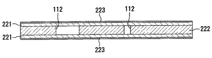
図2等に示されるように、前記セラミックコンデンサ10の複数箇所には、セラミックコンデンサ10をその厚さ方向に貫通する貫通孔111が形成されている。貫通孔111の形状は特に限定されないが、本実施形態における貫通孔111はセラミックコンデンサ10の厚さ方向から見て略円形状の貫通孔となっている。また、貫通孔111は、電極層11を貫通する電極層側貫通孔112と、前記誘電体層21を貫通して電極層側貫通孔112に連通する誘電体層側貫通孔113と、ニッケル電極31を貫通して電極層側貫通孔112及び誘電体層側貫通孔113に連通する導体層側貫通孔114とを含んで構成されている。なお、誘電体層側貫通孔113及び導体層側貫通孔114の内径は、互いに等しく、かつ、電極層側貫通孔112の内径よりも大きくなっている。そして、貫通孔111の内部には、樹脂層間絶縁層81,82の一部が入り込んでいる。
As shown in FIG. 2 and the like, through
図2等に示されるように、樹脂層間絶縁層81,82内には、銅からなる貫通ビア導体121と、同じく銅からなる非接触貫通ビア導体122とが設けられている。各ビア導体121,122は、セラミックコンデンサ10をその厚さ方向に貫通している。各ビア導体121,122の頂部は前記導体層125に面接触しており、各ビア導体121,122の底部はセラミックコンデンサ10よりも内層側に位置する内層側導体層123に面接触している。内層側導体層123は、前記コア基板72内にあるビア導体96に接続されている。
As shown in FIG. 2 and the like, the resin
貫通ビア導体121は、前記貫通孔111内に配置され、前記電極層11を貫通している。貫通ビア導体121の外周部は、前記電極層側貫通孔112の第1主面12側開口縁、内壁面及び第2主面13側開口縁に面接触している。即ち、貫通ビア導体121の第1主面12側(頂部側)の外径、及び、貫通ビア導体121の第2主面13側(底部側)の外径は、電極層側貫通孔112の内径よりも大きくなる一方、誘電体層側貫通孔113の内径及び導体層側貫通孔114の内径よりも小さくなっている。そして、貫通ビア導体121において電極層側貫通孔112内に位置する部分の外径は、電極層側貫通孔112の内径と等しくなっている。なお本実施形態において、内層側導体層123の表面から電極層11の第2主面13までの間隔は、内層側導体層123と貫通ビア導体121の底部との接触部分の直径の0.8倍である。
The through via
図2等に示されるように、前記非接触貫通ビア導体122は、貫通孔111内に配置され、電極層11、誘電体層21及びニッケル電極31に接触していない。即ち、非接触貫通ビア導体122の外径は、電極層側貫通孔112の内径、誘電体層側貫通孔113の内径及び導体層側貫通孔114の内径よりも小さくなっている。なお、非接触貫通ビア導体122が貫通する電極層側貫通孔112の内径は、貫通ビア導体121が貫通する電極層側貫通孔112の内径よりも大きくなっている。
As shown in FIG. 2 and the like, the non-contact through via
そして、このような構成のセラミックコンデンサ10に通電を行い、第1主面12側のニッケル電極31−電極層11間に所定の電圧を加えると、一方の電極にプラスの電荷が蓄積し、他方の電極にマイナスの電荷が蓄積するようになっている。
When the
次に、配線基板71の製造方法を図面に基づいて説明する。
Next, the manufacturing method of the
(1)誘電体グリーンシート221の作製
まず以下の手順で誘電体スラリーを調製した。平均粒径0.7μmのチタン酸バリウム粉末(誘電体粉)、エタノールとトルエンとの混合溶剤、分散剤、可塑剤をポットで湿式混合し、十分に混合された時点で、有機バインダを添加してさらに混合する。これにより、誘電体グリーンシート221を形成する際の出発材料となる誘電体スラリーを得る。このとき、各成分の配合比率を適宜変更することにより、誘電体スラリーを約0.5Pa・sの粘度(リオン株式会社製ビスコテスター VT−04型粘度計 No.1ロータ 62.5rpm 1分値 25℃で測定した粘度をいう。)に調製する。次に、この誘電体スラリーを用いて誘電体グリーンシート221の形成を以下のように行う。即ち、所定幅のPETフィルム223のロールを用意して、このロールをキャスティング装置の供給側にセットし、ドクターブレード法やリップコーティングなどの従来周知の手法によりPETフィルム223の上面に誘電体スラリーを薄く均一な厚さでキャスティング(塗工)する。その後、シート状にキャスティングされた誘電体スラリーをキャスティング装置の供給側と巻き取り側との間に配置されているヒータで加熱乾燥し、厚さ7μmの誘電体グリーンシート221(誘電体層21となる未焼結誘電体層)を形成する。
(1) Production of dielectric
(2)ニッケルグリーンシート220の作製
ニッケルグリーンシート220は、誘電体グリーンシート221の場合とほぼ同様の方法で作製される。まず、平均粒径0.7μmのニッケル粉末(金属粉)に分散剤、可塑剤を加える。これをターピネオールを分散媒として、さらに有機バインダを加えた上で混合する。次に、この混合物を用いて、ニッケルグリーンシート220の形成を行う。即ち、所定幅のPETフィルム225のロールを用意して、このロールをキャスティング装置の供給側にセットし、PETフィルム225の上面に上記の混合物を薄く均一な厚さでキャスティングする。その後、シート状にキャスティングされた混合物をヒータで加熱乾燥し、厚さ7μmのニッケルグリーンシート220(ニッケル電極31となる未焼結金属層)を形成する。
(2) Production of
(3)未焼結積層体50の作製
電極層11となる厚さ30μmのニッケル箔222を用意するとともに、そのニッケル箔222に対してエッチングを行う。これにより、ニッケル箔222が150mm角の大きさに切断され、ニッケル箔222に電極層側貫通孔112が形成される(貫通孔形成工程、図3参照)。また、打ち抜き金型等を用いて、各グリーンシート220,221をニッケル箔222と同じ大きさ(150mm角)に切断する。この段階ではまだグリーンシート220,221は硬化していないため、比較的簡単に打ち抜きを行うことができ、しかもクラックの発生を未然に防止することができる。
(3) Production of unsintered laminated body 50 A 30 μm-
そして次に、ニッケル箔222の両側に、誘電体層21となる誘電体グリーンシート221、及び、ニッケル電極31となるニッケルグリーンシート220をそれぞれ積層する。具体的に言うと、ニッケル箔222の両面にPETフィルム223付きの誘電体グリーンシート221を積層配置する(誘電体層積層工程、図4参照)。次に、ラミネート装置を用いて80℃で500kgf/cm2の条件で押圧力を加え、圧着させる。PETフィルム223を剥離した後、各誘電体グリーンシート221の剥離面上に、それぞれPETフィルム225付きのニッケルグリーンシート220を積層配置する(金属層形成工程、図5参照)。次に、ラミネート装置を用いて80℃で750kgf/cm2の条件で押圧力を加え、圧着させる。
Next, a dielectric
そして、PETフィルム225が付着したままの状態で、誘電体層21となる誘電体グリーンシート221、及び、ニッケル電極31となるニッケルグリーンシート220に対してレーザー孔あけ加工を行う。具体的には、レーザー径が前記電極層側貫通孔112の内径よりも大きくなるように調節した状態でレーザー孔あけ加工を行い、グリーンシート220,221を貫通して電極層側貫通孔112に連通する連通孔(誘電体層側貫通孔113と導体層側貫通孔114とからなる孔)を形成する(連通孔形成工程、図6参照)。なお、レーザー孔あけ加工は、ニッケル箔222の両側にある各グリーンシート220,221に対して行われる。
Then, with the
その結果、電極層側貫通孔112、誘電体層側貫通孔113及び導体層側貫通孔114からなる貫通孔111が焼成前に形成される。この後、汎用の切断機により25mm角に切断した後、PETフィルム225を剥離することにより未焼結積層体50(図6参照)を得る。この未焼結積層体50では、ニッケル箔222、誘電体グリーンシート221及びニッケルグリーンシート220が積層配置された状態となっている。
As a result, the through
(4)脱脂、同時焼成
次に、上記未焼結積層体50を大気中にて250℃で10時間脱脂し、さらに還元雰囲気中1260℃にて所定時間焼成する。その結果、チタン酸バリウム及びニッケルが加熱されて同時焼結し、厚さ4μmのニッケル電極31、厚さ4μmの誘電体層21、厚さ30μmの電極層11、厚さ4μmの誘電体層21、厚さ4μmのニッケル電極31の順で積層された焼結体(セラミックコンデンサ10)が得られる(焼成工程、図7参照)。
(4) Degreasing and simultaneous firing Next, the
(5)カップリング処理
次に、シランカップリング剤(KBM−403:信越化学製)の濃度が1wt%となる酢酸水溶液を調合する。これに焼成したセラミックコンデンサ10を1分含浸して引き上げる。そして、表面の余分なシランカップリング剤を洗い流した後、110℃で5分間乾燥させる。
(5) Coupling treatment Next, an acetic acid aqueous solution in which the concentration of the silane coupling agent (KBM-403: manufactured by Shin-Etsu Chemical Co., Ltd.) is 1 wt% is prepared. The fired
(6)第1層の樹脂層間絶縁層81の形成、セラミックコンデンサ10の実装
次に、第1層の樹脂層間絶縁層81が形成されたコア基板72を用意し、その第1層の樹脂層間絶縁層81上に、電極層11の第1主面12側を上向きにしてセラミックコンデンサ10を搭載する(図7,図8参照)。
(6) Formation of first resin
より詳細に言うと、第1層の樹脂層間絶縁層81を形成するための未硬化状態の樹脂層間絶縁層81(フィルム材)を用意し、それをラミネータ等でコア基板72の表面上に貼付する。次いで、加熱機構付きのマウンターを用いて、180℃で1分間加熱を行いながらセラミックコンデンサ10をフィルム材上に搭載し、所定の圧力で押し付ける。これに伴い、フィルム材の一部が前記貫通孔111内に入り込む。この時点で、フィルム材は、セラミックコンデンサ10の周辺部分のみが硬化する。
More specifically, an uncured resin interlayer insulation layer 81 (film material) for forming the first resin
なお、フィルム材としては、例えば、未硬化状態の熱硬化性樹脂からなるものが好適であり、セラミックコンデンサ10を搭載する前において熱処理を行うことによって最低溶融粘度を103Pa・s以上105Pa・s以下の範囲に設定したものが好適である。仮に、最低溶融粘度が103Pa・s未満であると、セラミックコンデンサ10をフィルム材上に搭載する際に、セラミックコンデンサ10が位置ずれしやすくなる。一方、最低溶融粘度が105Pa・sよりも大きいと、フィルム材の一部を貫通孔111内に入り込ませることが困難になる。
In addition, as a film material, what consists of an uncured thermosetting resin is suitable, for example, and minimum melt viscosity is 10 3 Pa.s or more and 10 5 by performing heat processing before mounting the
セラミックコンデンサ10の搭載後、150℃で30分間加熱する硬化工程を行い、フィルム材を硬化させて硬化状態の樹脂層間絶縁層81とする。これにより、第1層の樹脂層間絶縁層81にセラミックコンデンサ10が支持固定される。さらに、樹脂層間絶縁層81に対するビア穴あけを行った後、さらに銅めっきまたは銅ペーストの充填、印刷等を行って、ビア導体96を形成する。
After the
(7)樹脂ラミネート
次に、セラミックコンデンサ10上及び第1層の樹脂層間絶縁層81上に、未硬化状態のフィルム材をラミネータ等で被覆する。そして、熱硬化させて第2層(上層側)の樹脂層間絶縁層82とする(内蔵工程、図9参照)。この時点でセラミックコンデンサ10が樹脂層間絶縁層81,82内に完全に埋め込まれる。
(7) Resin Laminate Next, an uncured film material is covered with a laminator or the like on the
(8)レーザー加工
次に、炭酸ガスレーザーを用いたレーザー加工を行い、樹脂層間絶縁層82を貫通してニッケル電極31を露出させるビア孔229を形成する(図10参照)。また、レーザー径が内層側導体層123の直径及び電極層側貫通孔112の内径よりも小さくなるように調節した状態で炭酸ガスレーザーを用いたレーザー孔あけ加工を行い、樹脂層間絶縁層82、樹脂層間絶縁層81を順番に貫通して内層側導体層123を露出させるビア孔227を形成する。
(8) Laser Processing Next, laser processing using a carbon dioxide gas laser is performed to form a via
さらに、レーザー径が内層側導体層123の直径よりも小さく、かつ電極層側貫通孔112の内径よりも大きくなるように調節した状態で炭酸ガスレーザーを用いたレーザー孔あけ加工を行う。これにより、樹脂層間絶縁層82、樹脂層間絶縁層81を順番に貫通して内層側導体層123を露出させるビア孔228が電極層側貫通孔112を狙って形成される(ビア孔形成工程)。なお、レーザー孔あけ加工は、熱を発生する炭酸ガスレーザーを用いて行われるため、電極層側貫通孔112と同一軸線上にある樹脂層間絶縁層81,82だけでなく、電極層11の第2主面13側にある樹脂層間絶縁層81の一部も炭酸ガスレーザーの熱によって溶かされる。即ち、樹脂層間絶縁層81は、レーザー径よりも広い範囲で溶かされる。その結果、ビア孔228の内径は、電極層11の第1主面12側だけでなく、第2主面13側においても電極層側貫通孔112の内径以上の大きさとなる。なお、電極層11に炭酸ガスレーザーが遮られるにもかかわらず、第2主面13側にある樹脂層間絶縁層81が溶かされる理由としては、炭酸ガスレーザーの熱が内層側導体層123に反射して、内層側導体層123と電極層11との間にこもるためであると推測される。
Further, laser drilling using a carbon dioxide gas laser is performed in a state where the laser diameter is adjusted to be smaller than the diameter of the inner layer
(9)ビア形成
次に、過マンガン酸ナトリウムで樹脂層間絶縁層81,82を粗化し、各ビア孔227〜229の内面に対する無電解銅めっきを行った後、レジストを形成し、フォトリソでパターニングを行う。そして、電解銅めっきを行うことにより、ビア孔227,228内にビア導体121,122を形成するとともに、ビア孔229内にビア導体124を形成する(貫通ビア導体形成工程、図11参照)。その後、レジストを剥離し、レジスト下の無電解銅めっきを除去する。
(9) Via formation Next, the resin
(10)第3層,第4層の樹脂層間絶縁層83,84の形成
次に、第2層の樹脂層間絶縁層82に対するビア穴あけを行った後、さらに銅めっきまたは銅ペーストの充填、印刷等を行って、ビア導体96を形成するとともに、第2層の導体層92を形成する。この後、従来周知の手法により、第3層及び第4層(最表層)の樹脂層間絶縁層83,84の形成を行い、図1の配線基板71を完成させる。
(10) Formation of the third and fourth resin interlayer insulation layers 83 and 84 Next, after drilling via holes in the second resin
従って、本実施形態によれば以下の効果を得ることができる。 Therefore, according to the present embodiment, the following effects can be obtained.
(1)本実施形態の配線基板71によれば、貫通ビア導体121が、電極層側貫通孔112の第1主面12側開口縁及び内壁面に面接触する。それに加えて、貫通ビア導体121の外径が電極層側貫通孔112の内径よりも大きいために、貫通ビア導体121は、電極層11の第2主面13側に回り込んで第2主面13側開口縁にも面接触する。よって、貫通ビア導体121と電極層11との接触面積が大きくなり、両者の密着強度も大きくなる。ゆえに、配線基板71の製造時や使用時、または、熱サイクル試験等の信頼性試験を行う場合などに熱応力が作用したとしても、貫通ビア導体121と電極層11との間の剥離を防止できるため、貫通ビア導体121と電極層11との接続信頼性が高くなる。しかも、貫通ビア導体121が、電極層11を第1主面12側及び第2主面13側の両方から挟み込む構造であるため、貫通ビア導体121と電極層11との接触部分の一部が剥離したとしても、他の部分が接触状態を維持することができる。よって、貫通ビア導体121と電極層11との接続信頼性がよりいっそう高くなる。また、貫通ビア導体121の底部の直径が従来技術(図13の貫通ビア導体160を参照)よりも大きくなっている。よって、貫通ビア導体121の底部と内層側導体層123との接触面積が大きくなり、両者の密着強度も大きくなる。ゆえに、配線基板71の製造時や使用時、または、上記の信頼性試験を行う場合などに熱応力が作用したとしても、貫通ビア導体121の底部と内層側導体層123との剥離(デラミネーション)を防止できるため、貫通ビア導体121と内層側導体層123との接続信頼性が高くなる。よって、信頼性が高い配線基板71を実現することができる。
(1) According to the
(2)本実施形態では、樹脂層間絶縁層82を形成してセラミックコンデンサ10を樹脂層間絶縁層81,82内に埋め込む前に、セラミックコンデンサ10を支持する樹脂層間絶縁層81を硬化させている。このため、上層側の樹脂層間絶縁層82を被覆する際などに熱履歴を受けたとしても、セラミックコンデンサ10を支持する樹脂層間絶縁層81の流動が防止され、セラミックコンデンサ10の位置ずれが防止される。
[第2実施形態]
(2) In the present embodiment, the resin
[Second Embodiment]
次に、第2実施形態のコンデンサ内蔵配線基板を図面に基づいて詳細に説明する。ここでは第1実施形態と相違する部分を中心に説明し、共通する部分については同じ部材番号を付す代わりに説明を省略する。 Next, the capacitor built-in wiring board according to the second embodiment will be described in detail with reference to the drawings. Here, the description will focus on the parts that are different from the first embodiment, and the common parts will not be described in place of the same member numbers.
図12に示されるように、本実施形態の配線基板では、セラミックコンデンサの構造が前記第1実施形態とは異なっている。即ち、セラミックコンデンサ101は、2層のニッケル電極102,103が1層の誘電体層104を挟み込んだ構造を有している。詳述すると、第1ニッケル電極102の第1主面105は樹脂層間絶縁層82に面接触し、第1ニッケル電極102の第2主面106上には誘電体層104が形成されている。一方、第2ニッケル電極103(電極層)の第1主面107上には誘電体層104が形成され、第2ニッケル電極103の第2主面108全体は樹脂層間絶縁層81に面接触している。なお本実施形態では、ニッケル電極102,103の厚さが8μm、誘電体層104の厚さが4μmに設定されているため、セラミックコンデンサ101の全体の厚さは20μmとなっている。また、セラミックコンデンサ101には凹部226が形成されている。凹部226は、第1ニッケル電極102及び誘電体層104を貫通し、第2ニッケル電極103を露出させている。
As shown in FIG. 12, in the wiring board of the present embodiment, the structure of the ceramic capacitor is different from that of the first embodiment. That is, the
そして、図12に示される本実施形態の貫通ビア導体121は、前記第1実施形態の貫通ビア導体121とほぼ同様の構造を有している。即ち、貫通ビア導体121の外周部は、第2ニッケル電極103に形成された電極層側貫通孔109の第1主面107側開口縁、内壁面及び第2主面108側開口縁に面接触している。即ち、貫通ビア導体121の第1主面107側(頂部側)及び第2主面108側(底部側)の外径は、電極層側貫通孔109の内径よりも大きくなっている。
The through via
従って、本実施形態によれば、貫通ビア導体121と第2ニッケル電極103との接触面積が大きくなり、両者の密着強度も大きくなる。ゆえに、熱応力が作用した際の貫通ビア導体121と第2ニッケル電極103との間の剥離を防止でき、接続信頼性が高くなる。また、貫通ビア導体121の底部と内層側導体層123との接触面積が大きくなり、両者の密着強度も大きくなる。ゆえに、熱応力が作用した際の貫通ビア導体121の底部と内層側導体層123との剥離(デラミネーション)を防止でき、接続信頼性が高くなる。よって、信頼性が高い配線基板を実現することができる。
Therefore, according to the present embodiment, the contact area between the through via
次に、信頼性についての評価方法及びその結果を説明する。 Next, an evaluation method for reliability and a result thereof will be described.
まず、測定用サンプルを次のように準備した。第1実施形態と同じ配線基板71を準備し、これを実施例1とした。また、第2実施形態と同じ配線基板を準備し、これを実施例2とした。さらに、従来技術と同じ配線基板(図13参照)を準備し、これを比較例とした。
First, a measurement sample was prepared as follows. The
次に、各測定用サンプル(実施例1,2、比較例)に対してサーマルショックテストを実施した。具体的には、−40℃(1時間)〜80℃(1時間)を1サイクルとして繰り返し試験を行った。 Next, a thermal shock test was performed on each measurement sample (Examples 1 and 2 and Comparative Example). Specifically, the test was repeated with -40 ° C (1 hour) to 80 ° C (1 hour) as one cycle.
このように試験を行った結果、比較例の貫通ビア導体160は、電極層側貫通孔155の第1主面156側開口縁及び内壁面のみに面接触し、電極層154の第2主面157側に回り込まない構造であるため、貫通ビア導体160と電極層154との接触面積が実施例1,2よりも小さく、両者の密着強度も小さい。よって、サーマルショックテストを実施した際に作用した熱応力により、貫通ビア導体160と電極層154とが剥離してしまった。また、貫通ビア導体160の底部と内層側導体層161との接触面積が実施例1,2よりも小さく、両者の密着強度も小さい。よって、サーマルショックテストを実施した際に作用した熱応力により、貫通ビア導体160の底部と内層側導体層161とが剥離してしまった。従って、第1実施形態の配線基板71や第2実施形態の配線基板への比較例の採用は困難であることが証明された。
As a result of the test, the through via
一方、実施例1,2では、セラミックコンデンサ10と各ビア導体121,122,124との接続が維持されていた。また、各ビア導体121,122の底部と内層側導体層123との剥離(デラミネーション)が生じることもなかった。従って、第1,第2実施形態の配線基板の構造としては、最も問題が少ない実施例1,2の構造が適することが分かった。
On the other hand, in Examples 1 and 2, the connection between the
なお、各実施形態は以下のように変更してもよい。 Each embodiment may be changed as follows.
・上記第1実施形態のセラミックコンデンサ10は、電極層11の第1主面12上及び第2主面13上のそれぞれに、1層の誘電体層21と1層のニッケル電極31とを積層した構造を有していたが、電極層11、誘電体層21及びニッケル電極31の層数を変更してもよい。また、上記第2実施形態のセラミックコンデンサ101は、1層の誘電体層104と2層のニッケル電極102,103とを積層した構造を有していたが、誘電体層104及びニッケル電極102,103の層数を変更してもよい。
The
次に、前述した実施形態によって把握される技術的思想を以下に列挙する。 Next, the technical ideas grasped by the embodiment described above are listed below.
(1)第1主面及び第2主面を有する電極層と、前記電極層の前記第1主面及び前記第2主面の少なくともいずれかの上に形成された誘電体層とを有するコンデンサが、前記第2主面側を内層側に配置しかつ前記第1主面側を外層側に配置した状態で、配線基板における配線積層部を構成する樹脂層間絶縁層内に埋め込まれているコンデンサ内蔵配線基板であって、前記コンデンサをその厚さ方向に貫通する貫通ビア導体が、前記樹脂層間絶縁層内に設けられ、前記貫通ビア導体の底部が、前記コンデンサよりも内層側に位置する内層側導体層に面接触し、前記貫通ビア導体の頂部側の外径、及び、前記貫通ビア導体の底部側の外径が、前記電極層側貫通孔の内径よりも大きくなるとともに、前記貫通ビア導体において前記電極層側貫通孔内に位置する部分の外径が、前記電極層側貫通孔の内径と等しくなっており、前記貫通ビア導体の外周部が、前記電極層に形成された電極層側貫通孔の第1主面側開口縁、内壁面及び第2主面側開口縁に面接触していることを特徴とするコンデンサ内蔵配線基板。 (1) A capacitor having an electrode layer having a first main surface and a second main surface, and a dielectric layer formed on at least one of the first main surface and the second main surface of the electrode layer However, the capacitor embedded in the resin interlayer insulating layer constituting the wiring laminated portion in the wiring board in a state where the second main surface side is disposed on the inner layer side and the first main surface side is disposed on the outer layer side. An internal wiring board, wherein a through via conductor that penetrates the capacitor in the thickness direction is provided in the resin interlayer insulating layer, and an inner layer in which a bottom portion of the through via conductor is located on an inner layer side of the capacitor The outer diameter on the top side of the through via conductor and the outer diameter on the bottom side of the through via conductor are larger than the inner diameter of the electrode layer side through hole. In the electrode layer side through hole in the conductor The outer diameter of the portion located is equal to the inner diameter of the electrode layer side through hole, and the outer peripheral portion of the through via conductor is the first main surface side opening of the electrode layer side through hole formed in the electrode layer. A wiring board with a built-in capacitor, wherein the wiring board is in surface contact with the edge, the inner wall surface, and the opening edge on the second main surface side.
10,101…コンデンサとしてのセラミックコンデンサ
11…電極層
12,107…第1主面
13,108…第2主面
21,104…誘電体層
31…導体層としてのニッケル電極
71…コンデンサ内蔵配線基板(配線基板)
73…配線積層部としてのビルドアップ層
81,82,83,84…樹脂層間絶縁層
103…電極層としての第2ニッケル電極
109,112…電極層側貫通孔
113…連通孔を構成する誘電体層側貫通孔
114…連通孔を構成する導体層側貫通孔
121…貫通ビア導体
122…非接触貫通ビア導体
123…内層側導体層
220…未焼結金属層としてのニッケルグリーンシート
221…未焼結体誘電体層としての誘電体グリーンシート
222…金属箔としてのニッケル箔
228…ビア孔
DESCRIPTION OF SYMBOLS 10,101 ...
73 ... Build-up
Claims (10)
前記コンデンサをその厚さ方向に貫通する貫通ビア導体が、前記樹脂層間絶縁層内に設けられ、
前記貫通ビア導体の底部が、前記コンデンサよりも内層側に位置する内層側導体層に面接触し、
前記貫通ビア導体の外周部が、前記電極層に形成された電極層側貫通孔の第1主面側開口縁、内壁面及び第2主面側開口縁に面接触し、
前記貫通ビア導体は、前記樹脂層間絶縁層を貫通して前記内層側導体層を露出させるビア孔に充填されたフィルドビア導体であって、頂部から底部に行くに従って全体的に外径が徐々に小さくなる形状をなしており、
前記貫通ビア導体の頂部及び底部における外径が、前記電極層側貫通孔の内径よりも大きく、
前記内層側導体層と前記貫通ビア導体の底部との接触部分の直径が、前記電極層側貫通孔の内径よりも大きい
ことを特徴とするコンデンサ内蔵配線基板。 A capacitor having an electrode layer having a first main surface and a second main surface, and a dielectric layer formed on at least one of the first main surface and the second main surface of the electrode layer, A wiring board with a built-in capacitor embedded in a resin interlayer insulating layer constituting a wiring laminated portion in the wiring board in a state where the second main surface side is arranged on the inner layer side and the first main surface side is arranged on the outer layer side Because
A through via conductor that penetrates the capacitor in its thickness direction is provided in the resin interlayer insulating layer,
The bottom of the through via conductor is in surface contact with the inner conductor layer located on the inner layer side of the capacitor,
The outer peripheral portion of the through via conductor is in surface contact with the first main surface side opening edge, the inner wall surface and the second main surface side opening edge of the electrode layer side through hole formed in the electrode layer,
The through via conductor is a filled via conductor filled in a via hole that penetrates the resin interlayer insulating layer and exposes the inner layer side conductor layer, and the outer diameter gradually decreases from the top to the bottom. Has a shape that
Outside diameter at the top and bottom of the through via conductor, much larger than the inner diameter of the electrode layer side through holes,
The wiring board with a built-in capacitor , wherein a diameter of a contact portion between the inner layer side conductor layer and a bottom portion of the through via conductor is larger than an inner diameter of the electrode layer side through hole .
前記電極層側貫通孔は焼成前に形成されている
ことを特徴とする請求項1乃至3のいずれか1項に記載のコンデンサ内蔵配線基板。 The capacitor has a structure in which the dielectric layer and a conductor layer formed by simultaneous firing with the dielectric layer are laminated on at least one side of a metal foil to be the electrode layer,
The wiring board with a built-in capacitor according to any one of claims 1 to 3, wherein the electrode layer side through hole is formed before firing.
前記コンデンサを前記樹脂層間絶縁層上に搭載した後、前記コンデンサ上及び前記樹脂層間絶縁層上に上層側の樹脂層間絶縁層を被覆することにより、前記コンデンサを樹脂層間絶縁層内に埋め込む内蔵工程と、
前記内蔵工程後、レーザー径が前記電極層側貫通孔の内径以上になるように調節した状態で炭酸ガスレーザーを用いたレーザー孔あけ加工を行い、前記樹脂層間絶縁層を貫通するビア孔を前記電極層側貫通孔を狙って形成するビア孔形成工程と、
前記ビア孔形成工程後、前記ビア孔の内面に対するめっきを行うことにより、前記ビア孔内に前記貫通ビア導体を形成する貫通ビア導体形成工程と
を含むことを特徴とするコンデンサ内蔵配線基板の製造方法。 In the manufacturing method of the wiring board with a built-in capacitor according to any one of claims 1 to 6,
A step of embedding the capacitor in the resin interlayer insulation layer by mounting the capacitor on the resin interlayer insulation layer and then covering the capacitor and the resin interlayer insulation layer with an upper resin interlayer insulation layer. When,
After the incorporation step, laser drilling is performed using a carbon dioxide laser in a state where the laser diameter is adjusted to be equal to or larger than the inner diameter of the electrode layer side through hole, and the via hole penetrating the resin interlayer insulating layer is formed A via hole forming step aiming at the electrode layer side through hole; and
And a through via conductor forming step of forming the through via conductor in the via hole by plating the inner surface of the via hole after the via hole forming step. Method.
前記電極層となる金属箔に前記電極層側貫通孔を形成する貫通孔形成工程と、
前記金属箔上に前記誘電体層となる未焼結誘電体層を積層する誘電体層積層工程と、
前記誘電体層積層工程後、前記未焼結誘電体層上に、前記誘電体層と同時焼成によって形成される導体層となる未焼結金属層を形成する金属層形成工程と、
前記金属層形成工程後、前記未焼結誘電体層及び前記未焼結金属層に、前記未焼結誘電体層及び前記未焼結金属層を貫通し、前記電極層側貫通孔に連通する連通孔を形成する連通孔形成工程と、
前記未焼結誘電体層及び前記未焼結金属層を加熱して焼結させることにより、前記誘電体層及び前記導体層を得る焼成工程と
を経て形成されることを特徴とする請求項7乃至9のいずれか1項に記載のコンデンサ内蔵配線基板の製造方法。 The capacitor is
A through hole forming step of forming the electrode layer side through hole in the metal foil to be the electrode layer;
A dielectric layer laminating step of laminating an unsintered dielectric layer serving as the dielectric layer on the metal foil;
After the dielectric layer laminating step, a metal layer forming step for forming an unsintered metal layer on the unsintered dielectric layer to be a conductor layer formed by simultaneous firing with the dielectric layer;
After the metal layer forming step, the unsintered dielectric layer and the unsintered metal layer penetrate through the unsintered dielectric layer and the unsintered metal layer and communicate with the through hole on the electrode layer side. A communication hole forming step of forming a communication hole;
8. The unsintered dielectric layer and the unsintered metal layer are heated and sintered to form the dielectric layer and the conductor layer, and then formed through a firing step. The manufacturing method of the wiring board with a built-in capacitor according to any one of 1 to 9.
Priority Applications (1)
| Application Number | Priority Date | Filing Date | Title |
|---|---|---|---|
| JP2007204187A JP5122885B2 (en) | 2007-08-06 | 2007-08-06 | Capacitor-embedded wiring board and manufacturing method thereof |
Applications Claiming Priority (1)
| Application Number | Priority Date | Filing Date | Title |
|---|---|---|---|
| JP2007204187A JP5122885B2 (en) | 2007-08-06 | 2007-08-06 | Capacitor-embedded wiring board and manufacturing method thereof |
Publications (2)
| Publication Number | Publication Date |
|---|---|
| JP2009043768A JP2009043768A (en) | 2009-02-26 |
| JP5122885B2 true JP5122885B2 (en) | 2013-01-16 |
Family
ID=40444231
Family Applications (1)
| Application Number | Title | Priority Date | Filing Date |
|---|---|---|---|
| JP2007204187A Expired - Fee Related JP5122885B2 (en) | 2007-08-06 | 2007-08-06 | Capacitor-embedded wiring board and manufacturing method thereof |
Country Status (1)
| Country | Link |
|---|---|
| JP (1) | JP5122885B2 (en) |
Family Cites Families (3)
| Publication number | Priority date | Publication date | Assignee | Title |
|---|---|---|---|---|
| JP2001267748A (en) * | 2000-03-16 | 2001-09-28 | Hitachi Aic Inc | Multi-layered printed wiring board and its manufacturing method |
| JP2005045008A (en) * | 2003-07-22 | 2005-02-17 | Matsushita Electric Ind Co Ltd | Multilayer body and its producing process |
| JP5089880B2 (en) * | 2005-11-30 | 2012-12-05 | 日本特殊陶業株式会社 | Capacitor for wiring board built-in, wiring board with built-in capacitor and manufacturing method thereof |
-
2007
- 2007-08-06 JP JP2007204187A patent/JP5122885B2/en not_active Expired - Fee Related
Also Published As
| Publication number | Publication date |
|---|---|
| JP2009043768A (en) | 2009-02-26 |
Similar Documents
| Publication | Publication Date | Title |
|---|---|---|
| TWI453883B (en) | Parts built-in wiring substrate | |
| JP4773531B2 (en) | Wiring board and manufacturing method thereof | |
| JP2010087499A (en) | Method of manufacturing capacitor device | |
| JP2009260318A (en) | Component built-in wiring board | |
| KR100605454B1 (en) | Transcription material and manufacturing method thereof, and wiring board manufactured by using transcription material | |
| US11083090B2 (en) | Multi-layer ceramic electronic component, method of producing a multi-layer ceramic electronic component, and substrate with a built-in electronic component | |
| JP2009043769A (en) | Wiring substrate with built-in capacitor, its manufacturing method, and capacitor with support | |
| JP2010087266A (en) | Composite substrate, and method of manufacturing the same | |
| JP2002076637A (en) | Substrate incorporating chip component, and manufacturing method of the substrate | |
| JP2015095587A (en) | Multilayer wiring board | |
| JP5707710B2 (en) | Multilayer chip parts | |
| JP2012009556A (en) | Ceramic electronic component and method of manufacturing the same | |
| JP2006210536A (en) | Method of manufacturing electronic component and wiring board therewith | |
| JP4718314B2 (en) | Dielectric laminated structure, manufacturing method thereof, and wiring board | |
| JP5436177B2 (en) | Wiring board built-in component, manufacturing method thereof, and wiring board | |
| JP5122885B2 (en) | Capacitor-embedded wiring board and manufacturing method thereof | |
| JP5723577B2 (en) | Manufacturing method of electronic parts | |
| JP4051194B2 (en) | Multi-layer wiring board with built-in capacitor element | |
| JP2006100422A (en) | Multilayer capacitor and manufacturing method thereof | |
| JP4579673B2 (en) | Electronic component and manufacturing method thereof, wiring board with electronic component | |
| WO2007010705A1 (en) | Capacitor, method for manufacturing capacitor, substrate with built-in capacitor, and method for manufacturing substrate with built-in capacitor | |
| JP4429130B2 (en) | Manufacturing method of ceramic electronic component | |
| JP2004172412A (en) | Capacitor element and multilayer wiring board with built-in capacitor element | |
| JP2006032747A (en) | Laminated electronic component and its manufacturing method | |
| JP2006179742A (en) | Electronic component, manufacturing method thereof, wiring board provided therewith, and interfacial structure between metal and dielectric |
Legal Events
| Date | Code | Title | Description |
|---|---|---|---|
| A621 | Written request for application examination |
Free format text: JAPANESE INTERMEDIATE CODE: A621 Effective date: 20100706 |
|
| A977 | Report on retrieval |
Free format text: JAPANESE INTERMEDIATE CODE: A971007 Effective date: 20120112 |
|
| A131 | Notification of reasons for refusal |
Free format text: JAPANESE INTERMEDIATE CODE: A131 Effective date: 20120124 |
|
| A521 | Written amendment |
Free format text: JAPANESE INTERMEDIATE CODE: A523 Effective date: 20120316 |
|
| TRDD | Decision of grant or rejection written | ||
| A01 | Written decision to grant a patent or to grant a registration (utility model) |
Free format text: JAPANESE INTERMEDIATE CODE: A01 Effective date: 20121002 |
|
| A01 | Written decision to grant a patent or to grant a registration (utility model) |
Free format text: JAPANESE INTERMEDIATE CODE: A01 |
|
| A61 | First payment of annual fees (during grant procedure) |
Free format text: JAPANESE INTERMEDIATE CODE: A61 Effective date: 20121025 |
|
| FPAY | Renewal fee payment (event date is renewal date of database) |
Free format text: PAYMENT UNTIL: 20151102 Year of fee payment: 3 |
|
| R150 | Certificate of patent or registration of utility model |
Free format text: JAPANESE INTERMEDIATE CODE: R150 |
|
| R250 | Receipt of annual fees |
Free format text: JAPANESE INTERMEDIATE CODE: R250 |
|
| R250 | Receipt of annual fees |
Free format text: JAPANESE INTERMEDIATE CODE: R250 |
|
| LAPS | Cancellation because of no payment of annual fees |