JP5090929B2 - 高性能mems実装アーキテクチャ - Google Patents
高性能mems実装アーキテクチャ Download PDFInfo
- Publication number
- JP5090929B2 JP5090929B2 JP2007552187A JP2007552187A JP5090929B2 JP 5090929 B2 JP5090929 B2 JP 5090929B2 JP 2007552187 A JP2007552187 A JP 2007552187A JP 2007552187 A JP2007552187 A JP 2007552187A JP 5090929 B2 JP5090929 B2 JP 5090929B2
- Authority
- JP
- Japan
- Prior art keywords
- cover plate
- anchor
- layer
- active layer
- features
- Prior art date
- Legal status (The legal status is an assumption and is not a legal conclusion. Google has not performed a legal analysis and makes no representation as to the accuracy of the status listed.)
- Expired - Fee Related
Links
Images


Classifications
-
- G—PHYSICS
- G01—MEASURING; TESTING
- G01C—MEASURING DISTANCES, LEVELS OR BEARINGS; SURVEYING; NAVIGATION; GYROSCOPIC INSTRUMENTS; PHOTOGRAMMETRY OR VIDEOGRAMMETRY
- G01C19/00—Gyroscopes; Turn-sensitive devices using vibrating masses; Turn-sensitive devices without moving masses; Measuring angular rate using gyroscopic effects
- G01C19/56—Turn-sensitive devices using vibrating masses, e.g. vibratory angular rate sensors based on Coriolis forces
- G01C19/5719—Turn-sensitive devices using vibrating masses, e.g. vibratory angular rate sensors based on Coriolis forces using planar vibrating masses driven in a translation vibration along an axis
-
- G—PHYSICS
- G01—MEASURING; TESTING
- G01P—MEASURING LINEAR OR ANGULAR SPEED, ACCELERATION, DECELERATION, OR SHOCK; INDICATING PRESENCE, ABSENCE, OR DIRECTION, OF MOVEMENT
- G01P1/00—Details of instruments
- G01P1/02—Housings
- G01P1/023—Housings for acceleration measuring devices
-
- G—PHYSICS
- G01—MEASURING; TESTING
- G01P—MEASURING LINEAR OR ANGULAR SPEED, ACCELERATION, DECELERATION, OR SHOCK; INDICATING PRESENCE, ABSENCE, OR DIRECTION, OF MOVEMENT
- G01P15/00—Measuring acceleration; Measuring deceleration; Measuring shock, i.e. sudden change of acceleration
- G01P15/02—Measuring acceleration; Measuring deceleration; Measuring shock, i.e. sudden change of acceleration by making use of inertia forces using solid seismic masses
- G01P15/08—Measuring acceleration; Measuring deceleration; Measuring shock, i.e. sudden change of acceleration by making use of inertia forces using solid seismic masses with conversion into electric or magnetic values
- G01P15/0802—Details
-
- G—PHYSICS
- G01—MEASURING; TESTING
- G01P—MEASURING LINEAR OR ANGULAR SPEED, ACCELERATION, DECELERATION, OR SHOCK; INDICATING PRESENCE, ABSENCE, OR DIRECTION, OF MOVEMENT
- G01P15/00—Measuring acceleration; Measuring deceleration; Measuring shock, i.e. sudden change of acceleration
- G01P15/02—Measuring acceleration; Measuring deceleration; Measuring shock, i.e. sudden change of acceleration by making use of inertia forces using solid seismic masses
- G01P15/08—Measuring acceleration; Measuring deceleration; Measuring shock, i.e. sudden change of acceleration by making use of inertia forces using solid seismic masses with conversion into electric or magnetic values
- G01P15/125—Measuring acceleration; Measuring deceleration; Measuring shock, i.e. sudden change of acceleration by making use of inertia forces using solid seismic masses with conversion into electric or magnetic values by capacitive pick-up
-
- G—PHYSICS
- G01—MEASURING; TESTING
- G01P—MEASURING LINEAR OR ANGULAR SPEED, ACCELERATION, DECELERATION, OR SHOCK; INDICATING PRESENCE, ABSENCE, OR DIRECTION, OF MOVEMENT
- G01P15/00—Measuring acceleration; Measuring deceleration; Measuring shock, i.e. sudden change of acceleration
- G01P15/18—Measuring acceleration; Measuring deceleration; Measuring shock, i.e. sudden change of acceleration in two or more dimensions
-
- H—ELECTRICITY
- H01—ELECTRIC ELEMENTS
- H01L—SEMICONDUCTOR DEVICES NOT COVERED BY CLASS H10
- H01L2224/00—Indexing scheme for arrangements for connecting or disconnecting semiconductor or solid-state bodies and methods related thereto as covered by H01L24/00
- H01L2224/01—Means for bonding being attached to, or being formed on, the surface to be connected, e.g. chip-to-package, die-attach, "first-level" interconnects; Manufacturing methods related thereto
- H01L2224/42—Wire connectors; Manufacturing methods related thereto
- H01L2224/44—Structure, shape, material or disposition of the wire connectors prior to the connecting process
- H01L2224/45—Structure, shape, material or disposition of the wire connectors prior to the connecting process of an individual wire connector
- H01L2224/45001—Core members of the connector
- H01L2224/45099—Material
- H01L2224/451—Material with a principal constituent of the material being a metal or a metalloid, e.g. boron (B), silicon (Si), germanium (Ge), arsenic (As), antimony (Sb), tellurium (Te) and polonium (Po), and alloys thereof
- H01L2224/45138—Material with a principal constituent of the material being a metal or a metalloid, e.g. boron (B), silicon (Si), germanium (Ge), arsenic (As), antimony (Sb), tellurium (Te) and polonium (Po), and alloys thereof the principal constituent melting at a temperature of greater than or equal to 950°C and less than 1550°C
- H01L2224/45144—Gold (Au) as principal constituent
-
- H—ELECTRICITY
- H01—ELECTRIC ELEMENTS
- H01L—SEMICONDUCTOR DEVICES NOT COVERED BY CLASS H10
- H01L2224/00—Indexing scheme for arrangements for connecting or disconnecting semiconductor or solid-state bodies and methods related thereto as covered by H01L24/00
- H01L2224/01—Means for bonding being attached to, or being formed on, the surface to be connected, e.g. chip-to-package, die-attach, "first-level" interconnects; Manufacturing methods related thereto
- H01L2224/42—Wire connectors; Manufacturing methods related thereto
- H01L2224/47—Structure, shape, material or disposition of the wire connectors after the connecting process
- H01L2224/48—Structure, shape, material or disposition of the wire connectors after the connecting process of an individual wire connector
- H01L2224/4805—Shape
- H01L2224/4809—Loop shape
- H01L2224/48091—Arched
-
- H—ELECTRICITY
- H01—ELECTRIC ELEMENTS
- H01L—SEMICONDUCTOR DEVICES NOT COVERED BY CLASS H10
- H01L2924/00—Indexing scheme for arrangements or methods for connecting or disconnecting semiconductor or solid-state bodies as covered by H01L24/00
- H01L2924/01—Chemical elements
- H01L2924/01013—Aluminum [Al]
-
- H—ELECTRICITY
- H01—ELECTRIC ELEMENTS
- H01L—SEMICONDUCTOR DEVICES NOT COVERED BY CLASS H10
- H01L2924/00—Indexing scheme for arrangements or methods for connecting or disconnecting semiconductor or solid-state bodies as covered by H01L24/00
- H01L2924/01—Chemical elements
- H01L2924/01014—Silicon [Si]
-
- H—ELECTRICITY
- H01—ELECTRIC ELEMENTS
- H01L—SEMICONDUCTOR DEVICES NOT COVERED BY CLASS H10
- H01L2924/00—Indexing scheme for arrangements or methods for connecting or disconnecting semiconductor or solid-state bodies as covered by H01L24/00
- H01L2924/013—Alloys
- H01L2924/0132—Binary Alloys
- H01L2924/01322—Eutectic Alloys, i.e. obtained by a liquid transforming into two solid phases
-
- H—ELECTRICITY
- H01—ELECTRIC ELEMENTS
- H01L—SEMICONDUCTOR DEVICES NOT COVERED BY CLASS H10
- H01L2924/00—Indexing scheme for arrangements or methods for connecting or disconnecting semiconductor or solid-state bodies as covered by H01L24/00
- H01L2924/10—Details of semiconductor or other solid state devices to be connected
- H01L2924/102—Material of the semiconductor or solid state bodies
- H01L2924/1025—Semiconducting materials
- H01L2924/10251—Elemental semiconductors, i.e. Group IV
- H01L2924/10253—Silicon [Si]
-
- H—ELECTRICITY
- H01—ELECTRIC ELEMENTS
- H01L—SEMICONDUCTOR DEVICES NOT COVERED BY CLASS H10
- H01L2924/00—Indexing scheme for arrangements or methods for connecting or disconnecting semiconductor or solid-state bodies as covered by H01L24/00
- H01L2924/10—Details of semiconductor or other solid state devices to be connected
- H01L2924/146—Mixed devices
- H01L2924/1461—MEMS
Description
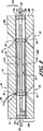
図は、シリコン・オン・インシュレータ(SOI)ウェーハのバルク機械加工および融着接合に基づいてセンサ・アーキテクチャを製作する本発明の方法を示し、この方法は、開ループモードか閉ループモードかのどちらかで動作する静電加速度計またはコリオリ・レートジャイロ・デバイスなどの対称でほぼ完全シリコンの密封封止超小型電子機械システム(MEMS)慣性デバイス1を製造する。
Claims (11)
- 超小型電気機械システム(MEMS)慣性デバイスであって、
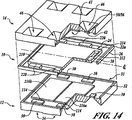
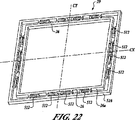
シリコン・オン・オキサイドウェーハ(16a)の活性層(22a)に形成された機構(10)であって、少なくとも1つの機構アンカー(28)によって構造的に支持された1つまたは複数のセンサ機械特徴(24)で構造化された機構(10)と、
シリコン・オン・オキサイドウェーハ(16b)で形成され、誘電体層(18b)によって半導体ハンドル層(20b)から隔離された半導体活性層(22b)を有する第1のカバープレート(12)と、前記第1のカバープレート活性層(22b)は、前記センサ機械特徴(24)と協働するように構造化された1つまたは複数の内部カバープレート特徴(31)および前記機構アンカー(28)と協働するように構造化されたカバープレート・アンカー(30)で構造化されており、前記第1のカバープレート・ハンドル層(20b)は、このハンドル層(20b)を通って前記カバープレート・アンカー(28)と一直線に並んで延びる穴特徴(34)で構造化されており、さらに、前記第1のカバープレート誘電体層(18b)は、前記カバープレート・アンカー(30)と前記穴特徴(34)の間に封止を形成する、誘電体材料でできた途切れのないリム(40)で構造化され、さらに前記カバープレート穴特徴(34)に近く、かつこの穴特徴(34)と一直線に並んだ前記カバープレート・アンカー(30)の表面(38)を露出させており、さらに、
前記機構アンカー(28)と前記カバープレート・アンカー(30)の間に形成された結合、を特徴とする超小型電気機械システム(MEMS)慣性デバイス。 - 前記カバープレート穴特徴(34)が、逆ピラミッド形を有して構造化されていることをさらに特徴とする、請求項1に記載の慣性デバイス。
- フレーム(26)が、前記1つまたは複数のセンサ機械特徴(24)および前記機構アンカー(28)を囲繞して前記機構活性層(22a)に形成され、さらに、前記第1のカバープレート活性層(22b)に形成された相補的なフレーム(32)に結合されていることをさらに特徴とする、請求項2に記載の慣性デバイス。
- 導電コネクタ(114)が、前記カバープレート・アンカー(30)と前記内部カバープレート特徴(31)の1つとの間で前記第1のカバープレート活性層に形成され、第2のカバープレート・アンカー(30)が前記第1のカバープレート活性層(22b)に形成されていることをさらに特徴とする、請求項3に記載の慣性デバイス。
- 第2のカバープレート(14)が、誘電体層(18c)で半導体ハンドル層(20c)から隔離された半導体活性層(22c)を有するシリコン・オン・オキサイドウェーハ(16c)で形成され、前記第2のカバープレート活性層(22c)は、前記センサ機械特徴(24)と協働するように構造化された1つまたは複数の内部カバープレート特徴(41)と、前記機構活性層(22a)に形成された前記フレーム(26)に対して相補的な、前記第1のカバープレート・フレーム(32)の反対側でこのフレーム(26)に結合されるフレーム(44)と、で構造化されていることをさらに特徴とする、請求項3に記載の慣性デバイス。
- 前記第2のカバープレート(14)が、前記センサ機械特徴(24)と協働するように構造化された1つまたは複数の内部カバープレート特徴(41)および前記機構アンカー(28)と協働するように構造化されたカバープレート・アンカー(42)で構造化される前記第2のカバープレート活性層(22c)を含んで前記第1のカバープレート(12)と実質的に同じに構造化され、前記第2のカバープレート・ハンドル層(20c)は、このハンドル層(20c)を通って前記カバープレート・アンカー(42)と一直線に並んで延びる穴特徴(46)で構造化されており、さらに、前記第2のカバープレート誘電体層(18)は、前記カバープレート・アンカー(42)と前記穴特徴(46)の間に封止を形成する、誘電体材料でできた途切れのないリム(52)で構造化され、さらに前記カバープレート穴特徴(46)に近くかつこの穴特徴(46)と一直線に並んだ前記カバープレート・アンカー(42)の表面(50)を露出させており、さらに、
結合が、前記機構アンカー(28)と前記第2のカバープレート活性層(22c)に形成された前記アンカー(42)との間に形成されること、をさらに特徴とする、請求項5に記載の慣性デバイス。 - 前記機構(10)の面内の放射方向膨張に対して順応性のあるフランジ(29)が、前記センサ機械特徴(24)および前記機構アンカー(28)を囲繞して前記フレーム(26)に結合されていることをさらに特徴とする、請求項6に記載の慣性デバイス。
- 前記機構(10)の前記1つまたは複数のセンサ機械特徴(24)、および前記第1および第2のカバープレート活性層(22b、22c)の各々に形成された前記1つまたは複数の内部カバープレート特徴(31、41)が、静電加速度計(100)を形成するように構造化されていることをさらに特徴とする、請求項6に記載の慣性デバイス。
- 前記機構(10)の前記1つまたは複数のセンサ機械特徴(24)、および前記第1および第2のカバープレート活性層(22b、22c)の各々に形成された前記1つまたは複数の内部カバープレート特徴(31、41)が、コリオリ・レートジャイロスコープ(400)を形成するように構造化されていることをさらに特徴とする、請求項6に記載の慣性デバイス。
- 前記穴特徴(34、36)が前記機構(10)の両面に形成されていることを特徴とする請求項1に記載の慣性デバイス。
- 超小型電気機械システム(MEMS)慣性デバイスを形成する方法であって、
半導体材料ハンドル層(20a)と半導体材料活性層(22a)の間に誘電体材料層(18a)を有する第1のシリコン・オン・オキサイドウェーハ(16a)の前記半導体材料活性層(22a)に、1つまたは複数の機構アンカー(28)で構造的に支持された1つまたは複数のセンサ機械特徴(24)を形成するステップと、
半導体材料ハンドル層(20b)と半導体材料活性層(22b)の間に誘電体材料層(18b)を有する第2のシリコン・オン・オキサイドウェーハ(16b)の前記半導体材料活性層(22b)に、慣性デバイス(1)を形成するために前記センサ機械特徴(24)と協働するように構造化された1つまたは複数の内部カバープレート特徴(31)および前記機構アンカー(28)と協働するように構造化された1つまたは複数のカバープレート・アンカー(30)を形成するステップと、
前記第2のシリコン・オン・オキサイドウェーハ(16b)の前記カバープレート半導体材料ハンドル層(20b)に、このハンドル層(20b)を通って前記カバープレート・アンカー(28)の1つと一直線に並んで延びる穴特徴(34)を形成するステップと、
前記第2のシリコン・オン・オキサイドウェーハ(16b)の前記カバープレート誘電体材料層(18b)に、前記カバープレート・アンカー(30)と前記穴特徴(34)の間でそのアンカー(30)と一直線に並んだ誘電体材料の途切れのないリム(40)を形成し、前記穴特徴(34)に近接し、一直線に並んだ前記カバープレート・アンカー(30)の表面(38)をさらに露出させるステップと、
前記内部カバープレート特徴(31)が前記センサ機械特徴(24)と協働するように前記センサ機械特徴(24)に対して位置付けされた状態で、前記カバープレート誘電体およびハンドル層(18b、20b)の反対側の前記協働カバープレート・アンカー(30)の表面(22b’)に前記機構アンカー(28)の第1の表面(22a’)を結合するステップと、
前記第1のシリコン・オン・オキサイドウェーハ(16a)の前記半導体材料ハンドル層(20a)および誘電体材料層(18a)を除去するステップと、を特徴とする方法。
Applications Claiming Priority (3)
| Application Number | Priority Date | Filing Date | Title |
|---|---|---|---|
| US11/040,208 US7238999B2 (en) | 2005-01-21 | 2005-01-21 | High performance MEMS packaging architecture |
| US11/040,208 | 2005-01-21 | ||
| PCT/US2006/001276 WO2006078564A1 (en) | 2005-01-21 | 2006-01-12 | High performance mems packaging archetecture |
Publications (3)
| Publication Number | Publication Date |
|---|---|
| JP2008528968A JP2008528968A (ja) | 2008-07-31 |
| JP2008528968A5 JP2008528968A5 (ja) | 2012-03-29 |
| JP5090929B2 true JP5090929B2 (ja) | 2012-12-05 |
Family
ID=36297244
Family Applications (1)
| Application Number | Title | Priority Date | Filing Date |
|---|---|---|---|
| JP2007552187A Expired - Fee Related JP5090929B2 (ja) | 2005-01-21 | 2006-01-12 | 高性能mems実装アーキテクチャ |
Country Status (4)
| Country | Link |
|---|---|
| US (1) | US7238999B2 (ja) |
| EP (1) | EP1853928A1 (ja) |
| JP (1) | JP5090929B2 (ja) |
| WO (1) | WO2006078564A1 (ja) |
Cited By (1)
| Publication number | Priority date | Publication date | Assignee | Title |
|---|---|---|---|---|
| US11656079B2 (en) | 2021-02-26 | 2023-05-23 | Kabushiki Kaisha Toshiba | Sensor and electronic device |
Families Citing this family (51)
| Publication number | Priority date | Publication date | Assignee | Title |
|---|---|---|---|---|
| US7495462B2 (en) * | 2005-03-24 | 2009-02-24 | Memsic, Inc. | Method of wafer-level packaging using low-aspect ratio through-wafer holes |
| US7371676B2 (en) * | 2005-04-08 | 2008-05-13 | Micron Technology, Inc. | Method for fabricating semiconductor components with through wire interconnects |
| US7611919B2 (en) * | 2005-04-21 | 2009-11-03 | Hewlett-Packard Development Company, L.P. | Bonding interface for micro-device packaging |
| US7393770B2 (en) * | 2005-05-19 | 2008-07-01 | Micron Technology, Inc. | Backside method for fabricating semiconductor components with conductive interconnects |
| US7307348B2 (en) * | 2005-12-07 | 2007-12-11 | Micron Technology, Inc. | Semiconductor components having through wire interconnects (TWI) |
| US7449765B2 (en) * | 2006-02-27 | 2008-11-11 | Texas Instruments Incorporated | Semiconductor device and method of fabrication |
| US20070243662A1 (en) * | 2006-03-17 | 2007-10-18 | Johnson Donald W | Packaging of MEMS devices |
| US20070246665A1 (en) * | 2006-04-20 | 2007-10-25 | Lafond Peter H | Mechanical isolation for mems devices |
| US7659612B2 (en) | 2006-04-24 | 2010-02-09 | Micron Technology, Inc. | Semiconductor components having encapsulated through wire interconnects (TWI) |
| US7615863B2 (en) * | 2006-06-19 | 2009-11-10 | Northrop Grumman Space & Missions Systems Corp. | Multi-dimensional wafer-level integrated antenna sensor micro packaging |
| US7690255B2 (en) * | 2006-08-31 | 2010-04-06 | Evigia Systems, Inc. | Three-axis inertial sensor and method of forming |
| CN100492016C (zh) * | 2006-11-17 | 2009-05-27 | 中国科学院上海微系统与信息技术研究所 | 微机械电容式加速度传感器及制作方法 |
| US7531443B2 (en) * | 2006-12-08 | 2009-05-12 | Micron Technology, Inc. | Method and system for fabricating semiconductor components with through interconnects and back side redistribution conductors |
| US20090085194A1 (en) * | 2007-09-28 | 2009-04-02 | Honeywell International Inc. | Wafer level packaged mems device |
| US7971483B2 (en) * | 2008-03-28 | 2011-07-05 | Honeywell International Inc. | Systems and methods for acceleration and rotational determination from an out-of-plane MEMS device |
| US7984648B2 (en) * | 2008-04-10 | 2011-07-26 | Honeywell International Inc. | Systems and methods for acceleration and rotational determination from an in-plane and out-of-plane MEMS device |
| JP5062146B2 (ja) * | 2008-11-21 | 2012-10-31 | 大日本印刷株式会社 | 物理量センサおよびその製造方法、ならびに電子機器 |
| JP4924663B2 (ja) * | 2008-12-25 | 2012-04-25 | 株式会社デンソー | 半導体装置およびその製造方法 |
| WO2010104064A1 (ja) * | 2009-03-13 | 2010-09-16 | アルプス電気株式会社 | Memsセンサ |
| US8215169B2 (en) | 2009-03-26 | 2012-07-10 | Honeywell International Inc. | Using pole pieces to guide magnetic flux through a MEMS device and method of making |
| US8115573B2 (en) * | 2009-05-29 | 2012-02-14 | Infineon Technologies Ag | Resonance frequency tunable MEMS device |
| US8072056B2 (en) * | 2009-06-10 | 2011-12-06 | Medtronic, Inc. | Apparatus for restricting moisture ingress |
| US8172760B2 (en) | 2009-06-18 | 2012-05-08 | Medtronic, Inc. | Medical device encapsulated within bonded dies |
| JP2013501941A (ja) * | 2009-08-13 | 2013-01-17 | メギット (サン ファン キャピストラーノ) インコーポレイテッド | 高g範囲加速度センサにおける最大化された双方向の対称的な減衰のためのプルーフマス |
| JP5640379B2 (ja) * | 2009-12-28 | 2014-12-17 | ソニー株式会社 | 半導体装置の製造方法 |
| US8666505B2 (en) | 2010-10-26 | 2014-03-04 | Medtronic, Inc. | Wafer-scale package including power source |
| US8569090B2 (en) * | 2010-12-03 | 2013-10-29 | Babak Taheri | Wafer level structures and methods for fabricating and packaging MEMS |
| US8424388B2 (en) | 2011-01-28 | 2013-04-23 | Medtronic, Inc. | Implantable capacitive pressure sensor apparatus and methods regarding same |
| US20130001710A1 (en) * | 2011-06-29 | 2013-01-03 | Invensense, Inc. | Process for a sealed mems device with a portion exposed to the environment |
| JP2013171009A (ja) * | 2012-02-23 | 2013-09-02 | Hitachi Automotive Systems Ltd | 慣性力センサ |
| JP5864332B2 (ja) * | 2012-03-29 | 2016-02-17 | 曙ブレーキ工業株式会社 | 静電容量型加速度センサの製造方法、製造装置および静電容量型加速度センサ |
| US20140151721A1 (en) * | 2012-11-30 | 2014-06-05 | Corning Incorporated | Phase transition cooling in led lighting devices |
| US9394164B2 (en) * | 2013-03-12 | 2016-07-19 | Taiwan Semiconductor Manufacturing Company, Ltd. | MEMS method and structure |
| EP3019442A4 (en) | 2013-07-08 | 2017-01-25 | Motion Engine Inc. | Mems device and method of manufacturing |
| WO2015042700A1 (en) | 2013-09-24 | 2015-04-02 | Motion Engine Inc. | Mems components and method of wafer-level manufacturing thereof |
| EP3028007A4 (en) | 2013-08-02 | 2017-07-12 | Motion Engine Inc. | Mems motion sensor and method of manufacturing |
| US9725310B2 (en) * | 2013-12-20 | 2017-08-08 | Taiwan Semiconductor Manufacturing Company, Ltd. | Micro electromechanical system sensor and method of forming the same |
| JP6590812B2 (ja) | 2014-01-09 | 2019-10-16 | モーション・エンジン・インコーポレーテッド | 集積memsシステム |
| JP5827365B2 (ja) * | 2014-04-09 | 2015-12-02 | ハネウェル・インターナショナル・インコーポレーテッド | ウェーハレベルでパッケージングされたデバイスを形成する方法 |
| US20170030788A1 (en) | 2014-04-10 | 2017-02-02 | Motion Engine Inc. | Mems pressure sensor |
| US11674803B2 (en) | 2014-06-02 | 2023-06-13 | Motion Engine, Inc. | Multi-mass MEMS motion sensor |
| DE102014210986A1 (de) * | 2014-06-10 | 2015-12-17 | Robert Bosch Gmbh | Mikromechanische Schichtenanordnung |
| WO2016090467A1 (en) | 2014-12-09 | 2016-06-16 | Motion Engine Inc. | 3d mems magnetometer and associated methods |
| GB201423311D0 (en) | 2014-12-29 | 2015-02-11 | Pilkington Group Ltd | Switchable device |
| US10407299B2 (en) | 2015-01-15 | 2019-09-10 | Motion Engine Inc. | 3D MEMS device with hermetic cavity |
| WO2017104103A1 (ja) * | 2015-12-17 | 2017-06-22 | パナソニックIpマネジメント株式会社 | 接続構造体 |
| US10330696B2 (en) | 2016-03-24 | 2019-06-25 | Northrop Grumman Systems Corporation | Accelerometer sensor system |
| US10473920B2 (en) * | 2016-08-24 | 2019-11-12 | Stmicroelectronics S.R.L. | Hermetically sealed MEMS mirror and method of manufacture |
| US10121742B2 (en) * | 2017-03-15 | 2018-11-06 | Amkor Technology, Inc. | Method of forming a packaged semiconductor device using ganged conductive connective assembly and structure |
| US10446550B2 (en) * | 2017-10-13 | 2019-10-15 | Globalfoundries Inc. | Cut inside replacement metal gate trench to mitigate N-P proximity effect |
| KR20200130473A (ko) * | 2018-04-03 | 2020-11-18 | 램 리써치 코포레이션 | Mems 코리올리 가스 유량 제어기 |
Family Cites Families (11)
| Publication number | Priority date | Publication date | Assignee | Title |
|---|---|---|---|---|
| FR2687777B1 (fr) * | 1992-02-20 | 1994-05-20 | Sextant Avionique | Micro-capteur capacitif a faible capacite parasite et procede de fabrication. |
| FR2687778B1 (fr) * | 1992-02-20 | 1994-05-20 | Sextant Avionique | Micro-capteur capacitif a capacite parasite reduite et procede de fabrication. |
| DE59304431D1 (de) * | 1993-05-05 | 1996-12-12 | Litef Gmbh | Mikromechanische Beschleunigungsmessvorrichtung und Verfahren zu deren Herstellung |
| US5476819A (en) * | 1993-07-26 | 1995-12-19 | Litton Systems, Inc. | Substrate anchor for undercut silicon on insulator microstructures |
| US6105427A (en) * | 1998-07-31 | 2000-08-22 | Litton Systems, Inc. | Micro-mechanical semiconductor accelerometer |
| KR100276429B1 (ko) | 1998-09-07 | 2000-12-15 | 정선종 | 미소 진공 구조체의 제작방법 |
| US6308569B1 (en) | 1999-07-30 | 2001-10-30 | Litton Systems, Inc. | Micro-mechanical inertial sensors |
| JP3771100B2 (ja) * | 2000-01-19 | 2006-04-26 | アルプス電気株式会社 | 静電容量検出型センサおよびジャイロスコープならびに入力装置 |
| FR2834282B1 (fr) * | 2001-12-28 | 2004-02-27 | Commissariat Energie Atomique | Procede de renforcement d'une microstructure mecanique |
| KR20030077754A (ko) * | 2002-03-27 | 2003-10-04 | 삼성전기주식회사 | 마이크로 관성센서 및 그 제조 방법 |
| JP4238724B2 (ja) * | 2003-03-27 | 2009-03-18 | 株式会社デンソー | 半導体装置 |
-
2005
- 2005-01-21 US US11/040,208 patent/US7238999B2/en not_active Expired - Fee Related
-
2006
- 2006-01-12 WO PCT/US2006/001276 patent/WO2006078564A1/en active Application Filing
- 2006-01-12 EP EP06718362A patent/EP1853928A1/en not_active Withdrawn
- 2006-01-12 JP JP2007552187A patent/JP5090929B2/ja not_active Expired - Fee Related
Cited By (1)
| Publication number | Priority date | Publication date | Assignee | Title |
|---|---|---|---|---|
| US11656079B2 (en) | 2021-02-26 | 2023-05-23 | Kabushiki Kaisha Toshiba | Sensor and electronic device |
Also Published As
| Publication number | Publication date |
|---|---|
| WO2006078564A1 (en) | 2006-07-27 |
| EP1853928A1 (en) | 2007-11-14 |
| JP2008528968A (ja) | 2008-07-31 |
| US7238999B2 (en) | 2007-07-03 |
| US20060163679A1 (en) | 2006-07-27 |
Similar Documents
| Publication | Publication Date | Title |
|---|---|---|
| JP5090929B2 (ja) | 高性能mems実装アーキテクチャ | |
| JP5021312B2 (ja) | 角速度センサ及びその製造方法 | |
| EP2414775B1 (en) | Environmentally robust disc resonator gyroscope | |
| US6939473B2 (en) | Method of making an X-Y axis dual-mass tuning fork gyroscope with vertically integrated electronics and wafer-scale hermetic packaging | |
| US8069726B2 (en) | X-Y axis dual-mass tuning fork gyroscope with vertically integrated electronics and wafer-scale hermetic packaging | |
| US7104129B2 (en) | Vertically integrated MEMS structure with electronics in a hermetically sealed cavity | |
| KR101105059B1 (ko) | 수직으로 집적화된 일렉트로닉스 및 웨이퍼 스케일 밀봉패키징을 갖는 x―y축 듀얼 매스 튜닝 포크자이로스코프를 제조 방법 | |
| JP5450451B2 (ja) | 垂直方向に集積した電子回路およびウェハスケール密封包装を含むx−y軸二重質量音叉ジャイロスコープ | |
| JP2007509346A5 (ja) | ||
| US20180074090A1 (en) | Multiple degree of freedom mems sensor chip and method for fabricating the same | |
| US8327706B2 (en) | Angular velocity detecting device | |
| US8847337B2 (en) | Processes and mounting fixtures for fabricating electromechanical devices and devices formed therewith | |
| JP5048344B2 (ja) | 分離応力アイソレータ | |
| WO2005069016A1 (en) | Coplanar proofmasses employable to sense acceleration along three axes | |
| US9731958B2 (en) | Microelectromechanical system and fabricating process having decoupling structure that includes attaching element for fastening to carrier |
Legal Events
| Date | Code | Title | Description |
|---|---|---|---|
| A621 | Written request for application examination |
Free format text: JAPANESE INTERMEDIATE CODE: A621 Effective date: 20080926 |
|
| RD04 | Notification of resignation of power of attorney |
Free format text: JAPANESE INTERMEDIATE CODE: A7424 Effective date: 20110913 |
|
| A131 | Notification of reasons for refusal |
Free format text: JAPANESE INTERMEDIATE CODE: A131 Effective date: 20111007 |
|
| A601 | Written request for extension of time |
Free format text: JAPANESE INTERMEDIATE CODE: A601 Effective date: 20120106 |
|
| A602 | Written permission of extension of time |
Free format text: JAPANESE INTERMEDIATE CODE: A602 Effective date: 20120116 |
|
| A524 | Written submission of copy of amendment under section 19 (pct) |
Free format text: JAPANESE INTERMEDIATE CODE: A524 Effective date: 20120207 |
|
| TRDD | Decision of grant or rejection written | ||
| A01 | Written decision to grant a patent or to grant a registration (utility model) |
Free format text: JAPANESE INTERMEDIATE CODE: A01 Effective date: 20120815 |
|
| A01 | Written decision to grant a patent or to grant a registration (utility model) |
Free format text: JAPANESE INTERMEDIATE CODE: A01 |
|
| A61 | First payment of annual fees (during grant procedure) |
Free format text: JAPANESE INTERMEDIATE CODE: A61 Effective date: 20120913 |
|
| FPAY | Renewal fee payment (event date is renewal date of database) |
Free format text: PAYMENT UNTIL: 20150921 Year of fee payment: 3 |
|
| R150 | Certificate of patent or registration of utility model |
Free format text: JAPANESE INTERMEDIATE CODE: R150 |
|
| LAPS | Cancellation because of no payment of annual fees |