JP5089212B2 - LIGHT EMITTING DEVICE, LED LAMP USING THE SAME, AND METHOD FOR MANUFACTURING LIGHT EMITTING DEVICE - Google Patents
LIGHT EMITTING DEVICE, LED LAMP USING THE SAME, AND METHOD FOR MANUFACTURING LIGHT EMITTING DEVICE Download PDFInfo
- Publication number
- JP5089212B2 JP5089212B2 JP2007077313A JP2007077313A JP5089212B2 JP 5089212 B2 JP5089212 B2 JP 5089212B2 JP 2007077313 A JP2007077313 A JP 2007077313A JP 2007077313 A JP2007077313 A JP 2007077313A JP 5089212 B2 JP5089212 B2 JP 5089212B2
- Authority
- JP
- Japan
- Prior art keywords
- light emitting
- emitting device
- light
- sealing body
- body layer
- Prior art date
- Legal status (The legal status is an assumption and is not a legal conclusion. Google has not performed a legal analysis and makes no representation as to the accuracy of the status listed.)
- Active
Links
Images


Classifications
-
- H—ELECTRICITY
- H01—ELECTRIC ELEMENTS
- H01B—CABLES; CONDUCTORS; INSULATORS; SELECTION OF MATERIALS FOR THEIR CONDUCTIVE, INSULATING OR DIELECTRIC PROPERTIES
- H01B1/00—Conductors or conductive bodies characterised by the conductive materials; Selection of materials as conductors
- H01B1/06—Conductors or conductive bodies characterised by the conductive materials; Selection of materials as conductors mainly consisting of other non-metallic substances
- H01B1/10—Conductors or conductive bodies characterised by the conductive materials; Selection of materials as conductors mainly consisting of other non-metallic substances sulfides
-
- F—MECHANICAL ENGINEERING; LIGHTING; HEATING; WEAPONS; BLASTING
- F21—LIGHTING
- F21K—NON-ELECTRIC LIGHT SOURCES USING LUMINESCENCE; LIGHT SOURCES USING ELECTROCHEMILUMINESCENCE; LIGHT SOURCES USING CHARGES OF COMBUSTIBLE MATERIAL; LIGHT SOURCES USING SEMICONDUCTOR DEVICES AS LIGHT-GENERATING ELEMENTS; LIGHT SOURCES NOT OTHERWISE PROVIDED FOR
- F21K9/00—Light sources using semiconductor devices as light-generating elements, e.g. using light-emitting diodes [LED] or lasers
- F21K9/20—Light sources comprising attachment means
- F21K9/23—Retrofit light sources for lighting devices with a single fitting for each light source, e.g. for substitution of incandescent lamps with bayonet or threaded fittings
- F21K9/232—Retrofit light sources for lighting devices with a single fitting for each light source, e.g. for substitution of incandescent lamps with bayonet or threaded fittings specially adapted for generating an essentially omnidirectional light distribution, e.g. with a glass bulb
-
- F—MECHANICAL ENGINEERING; LIGHTING; HEATING; WEAPONS; BLASTING
- F21—LIGHTING
- F21Y—INDEXING SCHEME ASSOCIATED WITH SUBCLASSES F21K, F21L, F21S and F21V, RELATING TO THE FORM OR THE KIND OF THE LIGHT SOURCES OR OF THE COLOUR OF THE LIGHT EMITTED
- F21Y2115/00—Light-generating elements of semiconductor light sources
- F21Y2115/10—Light-emitting diodes [LED]
-
- H—ELECTRICITY
- H01—ELECTRIC ELEMENTS
- H01L—SEMICONDUCTOR DEVICES NOT COVERED BY CLASS H10
- H01L2224/00—Indexing scheme for arrangements for connecting or disconnecting semiconductor or solid-state bodies and methods related thereto as covered by H01L24/00
- H01L2224/01—Means for bonding being attached to, or being formed on, the surface to be connected, e.g. chip-to-package, die-attach, "first-level" interconnects; Manufacturing methods related thereto
- H01L2224/26—Layer connectors, e.g. plate connectors, solder or adhesive layers; Manufacturing methods related thereto
- H01L2224/31—Structure, shape, material or disposition of the layer connectors after the connecting process
- H01L2224/32—Structure, shape, material or disposition of the layer connectors after the connecting process of an individual layer connector
- H01L2224/321—Disposition
- H01L2224/32151—Disposition the layer connector connecting between a semiconductor or solid-state body and an item not being a semiconductor or solid-state body, e.g. chip-to-substrate, chip-to-passive
- H01L2224/32221—Disposition the layer connector connecting between a semiconductor or solid-state body and an item not being a semiconductor or solid-state body, e.g. chip-to-substrate, chip-to-passive the body and the item being stacked
- H01L2224/32225—Disposition the layer connector connecting between a semiconductor or solid-state body and an item not being a semiconductor or solid-state body, e.g. chip-to-substrate, chip-to-passive the body and the item being stacked the item being non-metallic, e.g. insulating substrate with or without metallisation
-
- H—ELECTRICITY
- H01—ELECTRIC ELEMENTS
- H01L—SEMICONDUCTOR DEVICES NOT COVERED BY CLASS H10
- H01L2224/00—Indexing scheme for arrangements for connecting or disconnecting semiconductor or solid-state bodies and methods related thereto as covered by H01L24/00
- H01L2224/01—Means for bonding being attached to, or being formed on, the surface to be connected, e.g. chip-to-package, die-attach, "first-level" interconnects; Manufacturing methods related thereto
- H01L2224/42—Wire connectors; Manufacturing methods related thereto
- H01L2224/44—Structure, shape, material or disposition of the wire connectors prior to the connecting process
- H01L2224/45—Structure, shape, material or disposition of the wire connectors prior to the connecting process of an individual wire connector
- H01L2224/45001—Core members of the connector
- H01L2224/45099—Material
- H01L2224/451—Material with a principal constituent of the material being a metal or a metalloid, e.g. boron (B), silicon (Si), germanium (Ge), arsenic (As), antimony (Sb), tellurium (Te) and polonium (Po), and alloys thereof
- H01L2224/45117—Material with a principal constituent of the material being a metal or a metalloid, e.g. boron (B), silicon (Si), germanium (Ge), arsenic (As), antimony (Sb), tellurium (Te) and polonium (Po), and alloys thereof the principal constituent melting at a temperature of greater than or equal to 400°C and less than 950°C
- H01L2224/45124—Aluminium (Al) as principal constituent
-
- H—ELECTRICITY
- H01—ELECTRIC ELEMENTS
- H01L—SEMICONDUCTOR DEVICES NOT COVERED BY CLASS H10
- H01L2224/00—Indexing scheme for arrangements for connecting or disconnecting semiconductor or solid-state bodies and methods related thereto as covered by H01L24/00
- H01L2224/01—Means for bonding being attached to, or being formed on, the surface to be connected, e.g. chip-to-package, die-attach, "first-level" interconnects; Manufacturing methods related thereto
- H01L2224/42—Wire connectors; Manufacturing methods related thereto
- H01L2224/44—Structure, shape, material or disposition of the wire connectors prior to the connecting process
- H01L2224/45—Structure, shape, material or disposition of the wire connectors prior to the connecting process of an individual wire connector
- H01L2224/45001—Core members of the connector
- H01L2224/45099—Material
- H01L2224/451—Material with a principal constituent of the material being a metal or a metalloid, e.g. boron (B), silicon (Si), germanium (Ge), arsenic (As), antimony (Sb), tellurium (Te) and polonium (Po), and alloys thereof
- H01L2224/45138—Material with a principal constituent of the material being a metal or a metalloid, e.g. boron (B), silicon (Si), germanium (Ge), arsenic (As), antimony (Sb), tellurium (Te) and polonium (Po), and alloys thereof the principal constituent melting at a temperature of greater than or equal to 950°C and less than 1550°C
- H01L2224/45144—Gold (Au) as principal constituent
-
- H—ELECTRICITY
- H01—ELECTRIC ELEMENTS
- H01L—SEMICONDUCTOR DEVICES NOT COVERED BY CLASS H10
- H01L2224/00—Indexing scheme for arrangements for connecting or disconnecting semiconductor or solid-state bodies and methods related thereto as covered by H01L24/00
- H01L2224/01—Means for bonding being attached to, or being formed on, the surface to be connected, e.g. chip-to-package, die-attach, "first-level" interconnects; Manufacturing methods related thereto
- H01L2224/42—Wire connectors; Manufacturing methods related thereto
- H01L2224/44—Structure, shape, material or disposition of the wire connectors prior to the connecting process
- H01L2224/45—Structure, shape, material or disposition of the wire connectors prior to the connecting process of an individual wire connector
- H01L2224/45001—Core members of the connector
- H01L2224/45099—Material
- H01L2224/451—Material with a principal constituent of the material being a metal or a metalloid, e.g. boron (B), silicon (Si), germanium (Ge), arsenic (As), antimony (Sb), tellurium (Te) and polonium (Po), and alloys thereof
- H01L2224/45138—Material with a principal constituent of the material being a metal or a metalloid, e.g. boron (B), silicon (Si), germanium (Ge), arsenic (As), antimony (Sb), tellurium (Te) and polonium (Po), and alloys thereof the principal constituent melting at a temperature of greater than or equal to 950°C and less than 1550°C
- H01L2224/45147—Copper (Cu) as principal constituent
-
- H—ELECTRICITY
- H01—ELECTRIC ELEMENTS
- H01L—SEMICONDUCTOR DEVICES NOT COVERED BY CLASS H10
- H01L2224/00—Indexing scheme for arrangements for connecting or disconnecting semiconductor or solid-state bodies and methods related thereto as covered by H01L24/00
- H01L2224/01—Means for bonding being attached to, or being formed on, the surface to be connected, e.g. chip-to-package, die-attach, "first-level" interconnects; Manufacturing methods related thereto
- H01L2224/42—Wire connectors; Manufacturing methods related thereto
- H01L2224/44—Structure, shape, material or disposition of the wire connectors prior to the connecting process
- H01L2224/45—Structure, shape, material or disposition of the wire connectors prior to the connecting process of an individual wire connector
- H01L2224/45001—Core members of the connector
- H01L2224/45099—Material
- H01L2224/451—Material with a principal constituent of the material being a metal or a metalloid, e.g. boron (B), silicon (Si), germanium (Ge), arsenic (As), antimony (Sb), tellurium (Te) and polonium (Po), and alloys thereof
- H01L2224/45163—Material with a principal constituent of the material being a metal or a metalloid, e.g. boron (B), silicon (Si), germanium (Ge), arsenic (As), antimony (Sb), tellurium (Te) and polonium (Po), and alloys thereof the principal constituent melting at a temperature of greater than 1550°C
- H01L2224/45169—Platinum (Pt) as principal constituent
-
- H—ELECTRICITY
- H01—ELECTRIC ELEMENTS
- H01L—SEMICONDUCTOR DEVICES NOT COVERED BY CLASS H10
- H01L2224/00—Indexing scheme for arrangements for connecting or disconnecting semiconductor or solid-state bodies and methods related thereto as covered by H01L24/00
- H01L2224/01—Means for bonding being attached to, or being formed on, the surface to be connected, e.g. chip-to-package, die-attach, "first-level" interconnects; Manufacturing methods related thereto
- H01L2224/42—Wire connectors; Manufacturing methods related thereto
- H01L2224/47—Structure, shape, material or disposition of the wire connectors after the connecting process
- H01L2224/48—Structure, shape, material or disposition of the wire connectors after the connecting process of an individual wire connector
- H01L2224/4805—Shape
- H01L2224/4809—Loop shape
- H01L2224/48091—Arched
-
- H—ELECTRICITY
- H01—ELECTRIC ELEMENTS
- H01L—SEMICONDUCTOR DEVICES NOT COVERED BY CLASS H10
- H01L2224/00—Indexing scheme for arrangements for connecting or disconnecting semiconductor or solid-state bodies and methods related thereto as covered by H01L24/00
- H01L2224/01—Means for bonding being attached to, or being formed on, the surface to be connected, e.g. chip-to-package, die-attach, "first-level" interconnects; Manufacturing methods related thereto
- H01L2224/42—Wire connectors; Manufacturing methods related thereto
- H01L2224/47—Structure, shape, material or disposition of the wire connectors after the connecting process
- H01L2224/48—Structure, shape, material or disposition of the wire connectors after the connecting process of an individual wire connector
- H01L2224/481—Disposition
- H01L2224/48151—Connecting between a semiconductor or solid-state body and an item not being a semiconductor or solid-state body, e.g. chip-to-substrate, chip-to-passive
- H01L2224/48221—Connecting between a semiconductor or solid-state body and an item not being a semiconductor or solid-state body, e.g. chip-to-substrate, chip-to-passive the body and the item being stacked
- H01L2224/48225—Connecting between a semiconductor or solid-state body and an item not being a semiconductor or solid-state body, e.g. chip-to-substrate, chip-to-passive the body and the item being stacked the item being non-metallic, e.g. insulating substrate with or without metallisation
- H01L2224/48227—Connecting between a semiconductor or solid-state body and an item not being a semiconductor or solid-state body, e.g. chip-to-substrate, chip-to-passive the body and the item being stacked the item being non-metallic, e.g. insulating substrate with or without metallisation connecting the wire to a bond pad of the item
-
- H—ELECTRICITY
- H01—ELECTRIC ELEMENTS
- H01L—SEMICONDUCTOR DEVICES NOT COVERED BY CLASS H10
- H01L2224/00—Indexing scheme for arrangements for connecting or disconnecting semiconductor or solid-state bodies and methods related thereto as covered by H01L24/00
- H01L2224/73—Means for bonding being of different types provided for in two or more of groups H01L2224/10, H01L2224/18, H01L2224/26, H01L2224/34, H01L2224/42, H01L2224/50, H01L2224/63, H01L2224/71
- H01L2224/732—Location after the connecting process
- H01L2224/73251—Location after the connecting process on different surfaces
- H01L2224/73265—Layer and wire connectors
-
- H—ELECTRICITY
- H01—ELECTRIC ELEMENTS
- H01L—SEMICONDUCTOR DEVICES NOT COVERED BY CLASS H10
- H01L24/00—Arrangements for connecting or disconnecting semiconductor or solid-state bodies; Methods or apparatus related thereto
- H01L24/01—Means for bonding being attached to, or being formed on, the surface to be connected, e.g. chip-to-package, die-attach, "first-level" interconnects; Manufacturing methods related thereto
- H01L24/42—Wire connectors; Manufacturing methods related thereto
- H01L24/44—Structure, shape, material or disposition of the wire connectors prior to the connecting process
- H01L24/45—Structure, shape, material or disposition of the wire connectors prior to the connecting process of an individual wire connector
-
- H—ELECTRICITY
- H01—ELECTRIC ELEMENTS
- H01L—SEMICONDUCTOR DEVICES NOT COVERED BY CLASS H10
- H01L24/00—Arrangements for connecting or disconnecting semiconductor or solid-state bodies; Methods or apparatus related thereto
- H01L24/73—Means for bonding being of different types provided for in two or more of groups H01L24/10, H01L24/18, H01L24/26, H01L24/34, H01L24/42, H01L24/50, H01L24/63, H01L24/71
-
- H—ELECTRICITY
- H01—ELECTRIC ELEMENTS
- H01L—SEMICONDUCTOR DEVICES NOT COVERED BY CLASS H10
- H01L25/00—Assemblies consisting of a plurality of individual semiconductor or other solid state devices ; Multistep manufacturing processes thereof
- H01L25/03—Assemblies consisting of a plurality of individual semiconductor or other solid state devices ; Multistep manufacturing processes thereof all the devices being of a type provided for in the same subgroup of groups H01L27/00 - H01L33/00, or in a single subclass of H10K, H10N, e.g. assemblies of rectifier diodes
- H01L25/04—Assemblies consisting of a plurality of individual semiconductor or other solid state devices ; Multistep manufacturing processes thereof all the devices being of a type provided for in the same subgroup of groups H01L27/00 - H01L33/00, or in a single subclass of H10K, H10N, e.g. assemblies of rectifier diodes the devices not having separate containers
- H01L25/075—Assemblies consisting of a plurality of individual semiconductor or other solid state devices ; Multistep manufacturing processes thereof all the devices being of a type provided for in the same subgroup of groups H01L27/00 - H01L33/00, or in a single subclass of H10K, H10N, e.g. assemblies of rectifier diodes the devices not having separate containers the devices being of a type provided for in group H01L33/00
- H01L25/0753—Assemblies consisting of a plurality of individual semiconductor or other solid state devices ; Multistep manufacturing processes thereof all the devices being of a type provided for in the same subgroup of groups H01L27/00 - H01L33/00, or in a single subclass of H10K, H10N, e.g. assemblies of rectifier diodes the devices not having separate containers the devices being of a type provided for in group H01L33/00 the devices being arranged next to each other
-
- H—ELECTRICITY
- H01—ELECTRIC ELEMENTS
- H01L—SEMICONDUCTOR DEVICES NOT COVERED BY CLASS H10
- H01L2924/00—Indexing scheme for arrangements or methods for connecting or disconnecting semiconductor or solid-state bodies as covered by H01L24/00
- H01L2924/01—Chemical elements
- H01L2924/01015—Phosphorus [P]
-
- H—ELECTRICITY
- H01—ELECTRIC ELEMENTS
- H01L—SEMICONDUCTOR DEVICES NOT COVERED BY CLASS H10
- H01L2924/00—Indexing scheme for arrangements or methods for connecting or disconnecting semiconductor or solid-state bodies as covered by H01L24/00
- H01L2924/01—Chemical elements
- H01L2924/0102—Calcium [Ca]
-
- H—ELECTRICITY
- H01—ELECTRIC ELEMENTS
- H01L—SEMICONDUCTOR DEVICES NOT COVERED BY CLASS H10
- H01L2924/00—Indexing scheme for arrangements or methods for connecting or disconnecting semiconductor or solid-state bodies as covered by H01L24/00
- H01L2924/01—Chemical elements
- H01L2924/01047—Silver [Ag]
-
- H—ELECTRICITY
- H01—ELECTRIC ELEMENTS
- H01L—SEMICONDUCTOR DEVICES NOT COVERED BY CLASS H10
- H01L2924/00—Indexing scheme for arrangements or methods for connecting or disconnecting semiconductor or solid-state bodies as covered by H01L24/00
- H01L2924/01—Chemical elements
- H01L2924/01063—Europium [Eu]
-
- H—ELECTRICITY
- H01—ELECTRIC ELEMENTS
- H01L—SEMICONDUCTOR DEVICES NOT COVERED BY CLASS H10
- H01L2924/00—Indexing scheme for arrangements or methods for connecting or disconnecting semiconductor or solid-state bodies as covered by H01L24/00
- H01L2924/01—Chemical elements
- H01L2924/01078—Platinum [Pt]
-
- H—ELECTRICITY
- H01—ELECTRIC ELEMENTS
- H01L—SEMICONDUCTOR DEVICES NOT COVERED BY CLASS H10
- H01L2924/00—Indexing scheme for arrangements or methods for connecting or disconnecting semiconductor or solid-state bodies as covered by H01L24/00
- H01L2924/01—Chemical elements
- H01L2924/01079—Gold [Au]
-
- H—ELECTRICITY
- H01—ELECTRIC ELEMENTS
- H01L—SEMICONDUCTOR DEVICES NOT COVERED BY CLASS H10
- H01L2924/00—Indexing scheme for arrangements or methods for connecting or disconnecting semiconductor or solid-state bodies as covered by H01L24/00
- H01L2924/10—Details of semiconductor or other solid state devices to be connected
- H01L2924/11—Device type
- H01L2924/12—Passive devices, e.g. 2 terminal devices
- H01L2924/1204—Optical Diode
- H01L2924/12041—LED
-
- H—ELECTRICITY
- H01—ELECTRIC ELEMENTS
- H01L—SEMICONDUCTOR DEVICES NOT COVERED BY CLASS H10
- H01L2924/00—Indexing scheme for arrangements or methods for connecting or disconnecting semiconductor or solid-state bodies as covered by H01L24/00
- H01L2924/15—Details of package parts other than the semiconductor or other solid state devices to be connected
- H01L2924/181—Encapsulation
-
- H—ELECTRICITY
- H01—ELECTRIC ELEMENTS
- H01L—SEMICONDUCTOR DEVICES NOT COVERED BY CLASS H10
- H01L2924/00—Indexing scheme for arrangements or methods for connecting or disconnecting semiconductor or solid-state bodies as covered by H01L24/00
- H01L2924/19—Details of hybrid assemblies other than the semiconductor or other solid state devices to be connected
- H01L2924/191—Disposition
- H01L2924/19101—Disposition of discrete passive components
- H01L2924/19107—Disposition of discrete passive components off-chip wires
-
- H—ELECTRICITY
- H01—ELECTRIC ELEMENTS
- H01L—SEMICONDUCTOR DEVICES NOT COVERED BY CLASS H10
- H01L33/00—Semiconductor devices with at least one potential-jump barrier or surface barrier specially adapted for light emission; Processes or apparatus specially adapted for the manufacture or treatment thereof or of parts thereof; Details thereof
- H01L33/48—Semiconductor devices with at least one potential-jump barrier or surface barrier specially adapted for light emission; Processes or apparatus specially adapted for the manufacture or treatment thereof or of parts thereof; Details thereof characterised by the semiconductor body packages
- H01L33/50—Wavelength conversion elements
Abstract
Description
本発明は、発光装置およびその製造方法に関する。 The present invention relates to a light emitting device and a method for manufacturing the same.
近年、照明装置の光源としてLEDが多く用いられるようになってきている。LEDを使った照明装置の白色光を得る方法として、赤色LED、青色LEDおよび緑色LEDの三種類のLEDを用いる方法、青色LEDから発した励起光を変換して黄色光を発する蛍光体を用いる方法などがある。照明用光源としては、十分な輝度の白色光が要求されているために、LEDチップを複数個用いた照明装置が商品化されている。 In recent years, many LEDs have been used as light sources for lighting devices. As a method for obtaining white light of an illumination device using LEDs, a method using three types of LEDs, a red LED, a blue LED, and a green LED, and a phosphor that emits yellow light by converting excitation light emitted from the blue LED is used. There are methods. As a light source for illumination, white light with sufficient luminance is required, and lighting devices using a plurality of LED chips have been commercialized.
このような照明装置の一例として、たとえば特開2001−7405号公報(特許文献1)には、図22に模式的に示すような発光ダイオード201が開示されている。図22に示す例の発光ダイオード201は、カソード電極203とアノード電極204を有するガラスエポキシ基板202に、接着剤中に蛍光材を分散させた蛍光材含有層206を介して発光ダイオード素子205の裏面が固定されている。また図22に示す例の発光ダイオード201は、発光ダイオード素子205が、上面側を樹脂封止体207によって封止されており、樹脂封止体207の上面には補助蛍光材含有層208が形成されている。特許文献1には、このような構成を備えることによって、白色発光ダイオードの発光輝度の向上を図ると共に、色度のバラツキを抑えることができると記載されている。
As an example of such an illuminating device, for example, Japanese Unexamined Patent Application Publication No. 2001-7405 (Patent Document 1) discloses a
しかしながら、図22に示した発光ダイオード201では、発光ダイオード素子205が蛍光材含有層206を介してガラスエポキシ基板202に固定された構成であるため、発光ダイオード素子205で発生した熱が直接蛍光材含有層206中の蛍光材に放熱されてしまい、蛍光材が変質してしまうという問題が発生することが想定される。
However, in the light-
また、たとえば特開2004−71726号公報(特許文献2)には、図23に模式的に示すような発光装置301が開示されている。図23に示す例の発光装置301は、第1の凹部303およびこの第1の凹部303を含む第2の凹部304(第2の凹部304内に第1の凹部303が形成されている)を有するパッケージ302を備える。第1の凹部303内には、青色領域の光を発光可能なLEDチップ305が搭載され、このLEDチップ305を覆うようにして第1の凹部303を充填して第1の蛍光体層306が形成されている。また第2の凹部304内には青色領域の光を発光可能なLEDチップ307が搭載され、このLEDチップ307および第1の蛍光体層306を覆うようにして第2の凹部304を充填して第2の蛍光体層308が形成されている。また、図23に示す例の発光装置301では、パッケージ302には、リード電極309の正極および負極が一体的に形成されており、このリード電極309の正極および負極にLEDチップ305,307のn型電極およびp型電極はそれぞれ導電性ワイヤ310を用いて電気的に接続されている。特許文献2には、このような構成を備えることによって、周囲温度の変化による色度ズレの発生を抑えた発光装置を提供できると記載されている。
Further, for example, Japanese Patent Application Laid-Open No. 2004-71726 (Patent Document 2) discloses a
しかしながら図23に示した発光装置301では、パッケージ302に2箇所の凹部(第1の凹部303および第2の凹部304)を形成し、また、2個のLEDチップ305,307が搭載され、さらに2種類の材質の異なる蛍光体層(第1の蛍光体層306および第2の蛍光体層308)を備える複雑な構造であるため、このような発光装置301を製造するに際しては工程が煩雑であり、また製造コストも高いという問題がある。
本発明は、上記課題を解決するためになされたものであって、その目的とするところは、発光素子と蛍光体とを組み合わせた発光装置であって、蛍光体により色ズレなどが抑制できるとともに、容易に製造することができる発光装置、ならびにその製造方法を提供することである。 The present invention has been made to solve the above-described problems, and an object of the present invention is a light-emitting device in which a light-emitting element and a phosphor are combined, and the phosphor can suppress color misalignment and the like. An object of the present invention is to provide a light emitting device that can be easily manufactured, and a method for manufacturing the same.
本発明の発光装置は、金属基板と、前記金属基板上に形成され、厚み方向に貫通する複数個の貫通孔を有する絶縁基材と、前記絶縁基材の表面に形成された配線パターンと、前記貫通孔内の金属基板上に搭載され、前記配線パターンに電気的に接続された複数個の発光素子と、前記発光素子を覆うように形成され、蛍光体を含有する第1の封止体層とを備え、発光素子は全て、前記配線パターンを介して一つの正電極外部接続ランドおよび一つの負電極外部接続ランドと接続されることを特徴とする。 The light emitting device of the present invention, a metal substrate, an insulating base material formed on the metal substrate and having a plurality of through holes penetrating in the thickness direction, a wiring pattern formed on the surface of the insulating base material, A plurality of light emitting elements mounted on a metal substrate in the through hole and electrically connected to the wiring pattern, and a first sealing body formed so as to cover the light emitting elements and containing a phosphor All the light emitting elements are connected to one positive electrode external connection land and one negative electrode external connection land through the wiring pattern .
本発明の発光装置において、前記発光素子が互いに平行な複数の列を形成するように配置され、隣接する列間で共通に結線されたボンディングワイヤを介して配線パターンに電気的に接続されていることが好ましい。 In the light emitting device of the present invention, the light emitting elements are arranged so as to form a plurality of parallel rows, and are electrically connected to a wiring pattern via bonding wires commonly connected between adjacent rows. It is preferable .
また本発明の発光装置において、各貫通孔内に複数個の前記発光素子が一列に配置されて搭載され、この配置と平行となるように前記絶縁基材表面に前記配線パターンが複数形成されていることが好ましい。 In the light emitting device of the present invention, a plurality of the light emitting elements are arranged and mounted in each through hole, and a plurality of the wiring patterns are formed on the surface of the insulating base so as to be parallel to the arrangement. Preferably it is .
本発明はまた、金属基板と、前記金属基板上に形成された絶縁基材と、前記絶縁基材上に離間部を形成するようにして載置された金属板と、前記金属板上に搭載され、前記金属板に電気的に接続されているとともに、前記離間部を介して隣接する金属板にも電気的に接続されている複数個の発光素子と、前記発光素子を覆うように形成され、蛍光体を含有する第1の封止体層とを有する発光部とを備える発光装置についても提供する。 The present invention also includes a metal substrate, an insulating substrate formed on the metal substrate, a metal plate placed so as to form a separation portion on the insulating substrate, and mounted on the metal plate. A plurality of light emitting elements that are electrically connected to the metal plate and also electrically connected to an adjacent metal plate through the spacing portion, and are formed to cover the light emitting element. There is also provided a light-emitting device including a light-emitting unit including a first sealing body layer containing a phosphor .
本発明の発光装置において、前記発光素子が全て、前記配線パターンを介して一つの正電極外部接続ランドおよび一つの負電極外部接続ランドと接続されることが好ましい。 In the light emitting device of the present invention, it is preferable that all the light emitting elements are connected to one positive electrode external connection land and one negative electrode external connection land through the wiring pattern .
本発明の発光装置において、複数個の前記発光素子が複数の列に配置されて搭載され、この発光素子の列と平行な離間部を形成するように前記金属板が載置されていることが好ましい。 In the light-emitting device of the present invention, a plurality of the light-emitting elements are arranged and mounted in a plurality of rows, and the metal plate is placed so as to form a separation portion parallel to the row of light-emitting elements. Is preferred .
本発明の発光装置において、前記第1の封止体層が、互いに平行な複数の列を形成するように配置されて搭載された前記発光素子を列ごとに覆うように複数形成されていることが好ましい。 In the light emitting device of the present invention, a plurality of the first sealing body layers are formed so as to cover each of the light emitting elements arranged and mounted so as to form a plurality of parallel rows. Is preferred .
上述したいずれの本発明の発光装置においても、第1の封止体層が、発光素子を1個ずつ覆うように複数形成されていることが好ましい。 In any of the above-described light emitting devices of the present invention, it is preferable that a plurality of the first sealing body layers are formed so as to cover the light emitting elements one by one .
上述したいずれの本発明の発光装置においても、前記第1の封止体層が、前記発光素子全てを1つの第1の封止体層で覆うように形成されていることが好ましい。 In any of the light emitting devices of the present invention described above, it is preferable that the first sealing body layer is formed so as to cover all the light emitting elements with one first sealing body layer .
上述したいずれの本発明の発光装置においても、蛍光体を含有する第2の封止体層が、前記第1の封止体層の少なくとも一部を覆うように形成されていることが好ましい。 In any of the above-described light emitting devices of the present invention, it is preferable that the second sealing body layer containing the phosphor is formed so as to cover at least a part of the first sealing body layer .
上述したいずれの本発明の発光装置においても、蛍光体を含有する第2の封止体層が、複数形成されたうちの少なくともいずれかの第1の封止体層上に形成されていることが好ましい。 In any of the light emitting devices of the present invention described above, the second sealing body layer containing the phosphor is formed on at least one of the plurality of the first sealing body layers. Is preferred .
上述したいずれの本発明の発光装置においても、第1の封止体層が、方形状、六角形状、円形状または複数の直線状の平面形状を有することが好ましい。 In any of the light-emitting devices of the present invention described above, it is preferable that the first sealing body layer has a square shape, a hexagonal shape, a circular shape, or a plurality of linear planar shapes .
上述したいずれの本発明の発光装置も、液晶ディスプレイのバックライト光源または照明用光源として好適に用いられる。 Any of the light-emitting devices of the present invention described above can be suitably used as a backlight light source or illumination light source for a liquid crystal display .
本発明は、基板上に複数個の発光素子を搭載し、発光素子を外部電極に電気的に接続する工程と、発光素子を覆うように第1の蛍光体を含有する第1の封止体層を形成する工程と、第1の封止体層形成後の発光装置の色度特性を測定する工程と、測定された色度特性に応じて色度ずれを調整し得るように第1の封止体層上に第2の封止体層を形成する工程とを含む発光装置の製造方法についても提供する。 The present invention includes a step of mounting a plurality of light emitting elements on a substrate, electrically connecting the light emitting elements to external electrodes, and a first sealing body containing a first phosphor so as to cover the light emitting elements. A step of forming a layer, a step of measuring the chromaticity characteristics of the light emitting device after the formation of the first sealing body layer, and a first chromaticity deviation can be adjusted according to the measured chromaticity characteristics. There is also provided a method for manufacturing a light emitting device including a step of forming a second sealing body layer on the sealing body layer.
本発明によれば、発光素子と蛍光体とを組み合わせた発光装置であって、蛍光体により色ズレなどが抑制できるとともに、容易に製造することができる発光装置、ならびにその製造方法を提供することができる。 According to the present invention, there is provided a light emitting device in which a light emitting element and a phosphor are combined, a light emitting device that can suppress color misregistration and the like by the phosphor and can be easily manufactured, and a method for manufacturing the same. Can do.
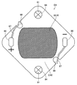
本発明の発光装置(第1の局面の発光装置)は、基板と、基板上に搭載され、外部電極に電気的に接続された複数個の発光素子と、発光素子を覆うように形成された第1の蛍光体を含有する第1の封止体層と、第1の封止体層上に形成された第2の蛍光体を含有する第2の封止体層とを備えることを特徴とする。このような本発明の発光装置によれば、色ズレなどが抑制できるとともに、容易に製造することができるという効果が奏される。このような本発明の第1の局面の発光装置の具体的構成例として、以下のような第2の局面の発光装置および第3の局面の発光装置を挙げることができる。なお、第1の局面の発光装置、第2の局面の発光装置および第3の局面の発光装置の全てに関して述べる場合には「本発明の発光装置」と総称する。 The light-emitting device of the present invention (the light-emitting device of the first aspect) is formed to cover a light-emitting element, a plurality of light-emitting elements mounted on the substrate and electrically connected to external electrodes. It is provided with the 1st sealing body layer containing the 1st fluorescent substance, and the 2nd sealing body layer containing the 2nd fluorescent substance formed on the 1st sealing body layer And According to such a light emitting device of the present invention, it is possible to suppress color misregistration and the like and to easily manufacture the device. Specific examples of the configuration of the light emitting device according to the first aspect of the present invention include the following light emitting device according to the second aspect and light emitting device according to the third aspect. Note that the light emitting device of the first aspect, the light emitting device of the second aspect, and the light emitting device of the third aspect are collectively referred to as “the light emitting device of the present invention”.
ここで、図1は、本発明の好ましい一例の第1の局面の発光装置D1を模式的に示す上面図である。また図2は、図1に示した例の第1の局面の発光装置D1が本発明の第2の局面の発光装置1として実現された場合の一例を模式的に示す断面図である。図2に示す本発明の第2の局面の発光装置1は、金属基板2と、金属基板2上に形成された絶縁基材3と、発光素子4と、第1の蛍光体を含有する第1の封止体層5と、第2の蛍光体を含有する第2の封止体層6とを基本的に備える。本発明の第2の局面の発光装置1において、絶縁基材3は、その表面に配線パターン7が形成されており、また厚み方向に貫通して複数個の貫通孔8が形成されている。また、図2に示すような本発明の第2の局面の発光装置1では、絶縁基材3の貫通孔8内において露出した金属基板2上に上面に2つの電極(図示せず)を有する発光素子4が搭載され、ボンディングワイヤWを用いて配線パターン7と電気的に接続されることで、外部電極に電気的に接続される。このように搭載された複数個の発光素子4は、ボンディングワイヤWごと覆われて第1の蛍光体を含有する第1の封止体層5で封止される。またこの第1の封止体層5上に、第2の蛍光体を含有する第2の封止体層6が形成されてなる。また、図2に示すように、配線パターン7が形成された絶縁基材3の第1の封止体層5により覆われていない領域には、通常、ソルダーレジスト9が形成される。
Here, FIG. 1 is a top view schematically showing the light emitting device D1 of the first aspect of a preferred example of the present invention. FIG. 2 is a cross-sectional view schematically showing an example in which the light emitting device D1 of the first aspect of the example shown in FIG. 1 is realized as the
本発明の第2の局面の発光装置1における複数個の発光素子4の配置の仕方は特に制限されるものではないが、一列に配置されて搭載されてなることが好ましい。また、図2に示すような本発明の第2の局面の発光装置1の場合には、1つの貫通孔8内に複数個の発光素子4が一列に配置されて搭載され、この直線状の配置と平行となるように絶縁基材3の表面に直線状の配線パターン7が形成されるように実現されることで、貫通孔8内で、発光素子4の間隔を適宜調整することができ、所望の発光輝度に合わせて発光素子4の搭載個数を調整することができるため好ましい。
The arrangement of the plurality of
また本発明の第2の局面の発光装置1では、複数個の発光素子4が互いに平行な複数の列を形成するように配置されて搭載されてなることが好ましい。このように平行な複数の列を形成するように配置されることで、面状の発光装置を実現することができる。なお、この場合には、互いに平行な複数の列を形成するように配置されて搭載された発光素子4が、隣接する列の間で互いに共通に結線されたボンディングワイヤを介して配線パターン7に電気的に接続されるように実現されてなることがさらに好ましい。
In the
本発明の発光装置において、第1の封止体層は、第1の蛍光体を含有するものであり、発光素子を覆うように形成されていればよい。たとえば、図1および図2には、全ての発光素子4を1つの第1の封止体層5で覆うように実現された例を示している。このように全ての発光素子4を1つの第1の封止体層5で覆うように形成することで、発光装置の輝度ムラを低減でき、第1の封止体層の厚みのバラツキを低減できるという利点がある。
In the light-emitting device of the present invention, the first sealing body layer contains the first phosphor and may be formed so as to cover the light-emitting element. For example, FIG. 1 and FIG. 2 show an example in which all the
ここで、図3は、本発明の好ましい他の例の第1の局面の発光装置D2を模式的に示す上面図である。また図4は、図3に示した例の第1の局面の発光装置D2が本発明の第2の局面の発光装置として実現された場合の一例を模式的に示す断面図である。なお、図3および図4に示す例の発光装置D2,11は、一部を除いては図1および図2に示した例の発光装置D1,1と同様であり、同様の構成を有する部分については同一の参照符を付して説明を省略する。本発明の発光装置では、第1の封止体層を、複数個の発光素子を1つの第1の封止体層で覆うように形成してもよい。図3および図4には、上述したように互いに平行な複数の列を形成するように金属基板12上に発光素子4が搭載され(より好ましくは、互いに平行な複数の列を形成するように配置されて搭載された発光素子4が隣接する列間で共通に結線されたボンディングワイヤを介して配線パターンに電気的に接続されてなる)、搭載された発光素子4を列ごとに覆うように第1の封止体層13を形成してなる例を示している。このように、互いに平行な複数の列を形成するように配置して搭載された発光素子4を列ごとに1つの第1の封止体層13で覆うように形成することで、直線状に配置された発光素子4の発光輝度が向上し、直線状の発光を強調することができるという利点がある。
Here, FIG. 3 is a top view schematically showing the light emitting device D2 of the first aspect of another preferred example of the present invention. FIG. 4 is a cross-sectional view schematically showing an example in which the light emitting device D2 of the first aspect of the example shown in FIG. 3 is realized as the light emitting device of the second aspect of the present invention. The light emitting devices D2 and 11 in the example shown in FIGS. 3 and 4 are the same as the light emitting devices D1 and 1 in the example shown in FIGS. 1 and 2 except for a part, and have the same configuration. Are denoted by the same reference numerals, and description thereof is omitted. In the light emitting device of the present invention, the first sealing body layer may be formed so as to cover a plurality of light emitting elements with one first sealing body layer. 3 and 4, the light-emitting
また図5は、本発明の好ましいさらに他の例の第1の局面の発光装置D3を模式的に示す上面図である。なお、図5に示す例の第1の局面の発光装置D3は、一部を除いては図1および図3にそれぞれ示した例の第1の局面の発光装置D1,D2と同様であり、同様の構成を有する部分については同一の参照符を付して説明を省略する。図5には、発光素子4を1個ずつ覆うように第1の封止体層21が複数個形成されてなる例を示している。このように発光素子4を1個ずつ覆うように第1の封止体層21を形成する場合には、個々の発光素子4の発光輝度が向上し、点状の発光を強調することができるという利点がある。
FIG. 5 is a top view schematically showing a light emitting device D3 according to a first aspect of still another preferred example of the present invention. The light emitting device D3 of the first aspect of the example shown in FIG. 5 is the same as the light emitting devices D1 and D2 of the first aspect of the example shown in FIGS. Parts having the same configuration are denoted by the same reference numerals and description thereof is omitted. FIG. 5 shows an example in which a plurality of first sealing body layers 21 are formed so as to cover the
本発明の第2の局面の発光装置において、第2の封止体層は、第1の封止体層の少なくとも一部を覆うように形成されればよい。図1および図2には、第1の封止体層5上の一部の領域を覆うようにして第2の封止体層6が形成されてなる例を示している。また図3および図4には、上述のように互いに平行な複数の列を形成するように配置して搭載された発光素子4を列ごとに覆うように形成された複数の第1の封止体層13のうち、一部の第1の封止体層13を部分的に覆うようにして第2の封止体層13が形成された例を示している。また図5には、発光素子4を1個ずつ覆うように形成された複数の第1の封止体層21のうち、一部の第1の封止体層21のみを覆って第2の封止体層22が複数形成された例を示している。このように第1の封止体層5,13,21を部分的に覆うようにして第2の封止体層6,14,22を形成することで、第1の封止体層の一部のみの調整で発光装置として所望の色度特性を有する(たとえば、後述する色度座標を示す図21の(b)の範囲内に入る)発光装置を得ることができるという利点がある。なお、このような場合、第2の封止体層6,14,22にて覆う第1の封止体層5,13,21の部分は、所望の色度特性に応じて選択する(たとえば、後述する色度座標を示す図21の(b)の範囲内に入っていない部分など)。また第1の封止体層5,13,21を部分的に覆うようにして第2の封止体層6,14,22を形成する場合、第2の封止体層は複数(図1、図3に示す例では2つ、図5に示す例では5つ)形成するようにしても勿論よい。なお、第1の蛍光体を含有する第1の封止体層と、第2の蛍光体を含有する第2の封止体層の境界は、明確に分離していても、明確に分離していなくともよい。
In the light emitting device according to the second aspect of the present invention, the second sealing body layer may be formed so as to cover at least a part of the first sealing body layer. 1 and 2 show an example in which the second
ここで、図6は、本発明の好ましいさらに他の例の第1の局面の発光装置D4を模式的に示す上面図である。図7は、図6に示した例の第1の局面の発光装置D4が本発明の第2の局面の発光装置31として実現された場合の一例を模式的に示す断面図である。なお、図6および図7に示す例の発光装置D4,31は、一部を除いては図1および図2に示した例の発光装置D1,1と同様であり、同様の構成を有する部分については同一の参照符を付して説明を省略する。図6および図7に示す発光装置D4,31では、全ての発光素子4を覆うように1つの第1の封止体層5が形成されているのは図1および図2に示した例と同様であるが、この第1の封止体層5の上面全面を覆うようにして第2の封止体層32が形成されてなる。このように、第1の封止体層5の全部を覆って第2の封止体層32を形成してなることで、第1の封止体層5の上面全部について、後述する図21に示す色度座標において(b)の範囲内に入るように色度が調整された発光装置D4,31を実現することができるというような利点がある。
Here, FIG. 6 is a top view schematically showing the light emitting device D4 of the first aspect of still another preferred example of the present invention. FIG. 7 is a cross-sectional view schematically showing an example in which the light emitting device D4 according to the first aspect of the example shown in FIG. 6 is realized as the
次に、本発明の第1の局面の発光装置のもう1つの具体的構成例である第3の局面の発光装置について説明する。図8は、図1に示した例の発光装置D1が本発明の第3の局面の発光装置41で実現された場合の一例を模式的に示す断面図である。図8に示す本発明の第3の局面の発光装置41は、金属基板42上に形成された絶縁基材43と、絶縁基材43上に離間部45を形成するようにして載置された金属板44と、金属板44上に搭載された複数個の発光素子46と、第1の蛍光体を含有する第1の封止体層47と、第2の蛍光体を含有する第2の封止体層48とを基本的に備える。図8に示すように、本発明の第3の局面の発光装置41において、発光素子46は、当該発光素子46が搭載された金属板44に隣接する金属板44にも電気的に接続されてなる。なお、図8に示すような本発明の第3の局面の発光装置41は、発光素子46として上面に2つの電極(図示せず)を有するものを用い、ボンディングワイヤWを用いて各電極を金属板44にそれぞれ電気的に接続されてなることで、外部電極に電気的に接続されてなる。図8に示す例では、金属板44上の発光素子46を搭載する領域以外のいずれかの領域にはソルダーレジスト49が設けられてなる。また、本発明の第3の局面の発光装置41では、図8に示す例のように、金属板44上に金属メッキ50が形成され、この金属メッキ50上に発光素子46が搭載され、発光素子46はこの金属メッキ50を介して、上述した発光素子46が搭載された金属板44および当該金属板44に離間部45を介して隣接する金属板44に電気的に接続されてなることが好ましい。
Next, the light emitting device of the third aspect which is another specific configuration example of the light emitting device of the first aspect of the present invention will be described. FIG. 8 is a cross-sectional view schematically showing an example in which the light-emitting device D1 of the example shown in FIG. 1 is realized by the light-emitting
本発明の第3の局面の発光装置41における複数個の発光素子46の配置の仕方についても特に制限されるものではないが、上述した第2の局面の発光装置と同様に、一列に配置されて搭載されてなることが好ましい。また、図8に示すような本発明の第3の局面の発光装置41の場合には、複数個の発光素子46が一列に配置されて搭載され、この発光素子46の列と平行な離間部45を形成するように金属板44が載置されるように実現されることが好ましい。このように実現されることで、発光素子を搭載する際の目安となり、直線状に発光素子を配置しやすいという利点がある。さらには、本発明の第3の局面の発光装置41でも、上述した第2の局面の発光装置の場合と同様に、複数個の発光素子46が互いに平行な複数の列を形成するように配置されて搭載されてなることが好ましい。
The arrangement of the plurality of light-emitting
図8には、図2に示した例の第2の局面の発光装置1と同様に、全ての発光素子46を1つの第1の封止体層47で覆うように実現された例を示している。このように第3の局面の発光装置41でも、全ての発光素子46を1つの第1の封止体層47で覆うことによる上述した効果が同様に奏される。
FIG. 8 shows an example in which all the
また図9は、図3に示した例の第1の局面の発光装置D2が本発明の第3の局面の発光装置として実現された場合の一例を模式的に示す断面図である。なお、図9に示す例の発光装置51は、一部を除いては図8に示した例の発光装置41と同様であり、同様の構成を有する部分については同一の参照符を付して説明を省略する。図9には、互いに平行な複数の列を形成するように金属メッキ50を介して金属板44上に発光素子46が搭載され、搭載された発光素子46を列ごとに覆うように第1の封止体層53を形成してなる例を示している。このように、第3の局面の発光装置51の場合でも、互いに平行な複数の列を形成するように配置して搭載された発光素子46を列ごとに1つの第1の封止体層53で覆うように形成すれば、第2の局面の発光装置において同様に実現した場合と同様の上述した効果が奏される。
FIG. 9 is a cross-sectional view schematically showing an example in which the light emitting device D2 of the first aspect of the example shown in FIG. 3 is realized as the light emitting device of the third aspect of the present invention. The
なお、発光素子を1個ずつ覆うように第1の封止体層を形成してなる、図5に示した例の第1の局面の発光装置D3を、第3の局面の発光装置の構造にて実現するようにしても勿論よい。 Note that the light emitting device D3 of the first aspect of the example shown in FIG. 5 formed by forming the first sealing body layer so as to cover the light emitting elements one by one is the structure of the light emitting device of the third aspect. Of course, it may be realized by the above.
また図10は、図6に示した例の第1の局面の発光装置D4が本発明の第3の局面の発光装置61として実現された場合の一例を模式的に示す断面図である。なお、図10に示す例の発光装置61は、一部を除いては図8に示した例の発光装置41と同様であり、同様の構成を有する部分については同一の参照符を付して説明を省略する。図10に示す例の発光装置61は、全ての発光素子46を覆うように1つの第1の封止体層47が形成されているのは図8に示した例と同様であるが、この第1の封止体層47の上面全面を覆うようにして第2の封止体層62が形成されてなる。このように、図7に示した第2の局面の発光装置31と同様の構成を、図10に示すように第3の局面の発光装置でも実現すれば、上述と同様の効果が奏される。
FIG. 10 is a cross-sectional view schematically showing an example in which the light emitting device D4 of the first aspect of the example shown in FIG. 6 is realized as the
本発明の発光装置において、第1の封止体層の形状は特に制限されるものではないが、方形状、六角形状、円形状または複数の直線状の平面形状を有することが好ましい。ここで、第1の封止体層の平面形状とは、第1の封止体層の金属基板に平行な平面における形状を指す。上述した図1、図6に示す例の発光装置D1,D4は、第1の封止体層5,47が方形状の平面形状を有する場合であり、このように方形状の平面形状を有するように第1の封止体層5,47を形成する場合には、後述する固定用穴、外部配線用穴などを形成できる領域を確保できるという利点がある。また、上述した図3に示す例の発光装置D2は、第1の封止体層13,53が複数の直線状の平面形状を有する場合であり、このように複数の直線状の平面形状を有するように第1の封止体層13,53を形成する場合には、直線状に配置された発光素子の発光輝度が向上し、直線状に発光を強調することができるという利点がある。
In the light emitting device of the present invention, the shape of the first sealing body layer is not particularly limited, but preferably has a square shape, a hexagonal shape, a circular shape, or a plurality of linear planar shapes. Here, the planar shape of the first sealing layer, refers to the shape that put on a plane parallel to the metal substrate of the first sealing layer. Figure 1 described above, the light emitting device D1, D4 in the example shown in FIG. 6 shows the case where the
また図11は、本発明の好ましい他の例の第1の局面の発光装置D5を模式的に示す上面図である。なお、図11に示す発光装置D5は、一部を除いては図3に示した例の発光装置D2と同様であり、同様の構成を有する部分については同一の参照符を付して説明を省略する。図11には、発光素子(図示せず)全てを1つの第1の封止体層で覆うようにして平面形状が六角形状である第1の封止体層71が形成され、この第1の封止体層71を部分的に覆うようにして第2の封止体層72が形成されてなる場合の第1の局面の発光装置D5を示している。図11に示す例のように六角形状の平面形状を有するように第1の封止体層71を形成する場合には、対称形状であるため光指向性がよいという利点がある。
FIG. 11 is a top view schematically showing a light emitting device D5 according to a first aspect of another preferred example of the present invention. The light-emitting device D5 shown in FIG. 11 is the same as the light-emitting device D2 in the example shown in FIG. 3 except for a part, and the same reference numerals are given to the portions having the same configuration. Omitted. In FIG. 11, a first
また、図12は、本発明の好ましいさらに他の例の第1の局面の発光装置D6を模式的に示す上面図である。なお、図12に示す発光装置D6は、一部を除いては図3に示した例の発光装置D2と同様であり、同様の構成を有する部分については同一の参照符を付して説明を省略する。図12には、発光素子(図示せず)全てを1つの第1の封止体層で覆うようにして平面形状が円形状である第1の封止体層76が形成され、この第1の封止体層76を部分的に覆うようにして第2の封止体層77が形成されてなる場合の第1の局面の発光装置D6を示している。また上述した図5に示した例の発光装置D3は、発光素子を1個ずつ覆うようにして形成された第1の封止体層21が円形状の平面形状を有する場合である。図5,12に示す例のように円形状の平面形状を有するように第1の封止体層21,76を形成する場合には、対称形状であるため光指向性がよいという利点がある。
FIG. 12 is a top view schematically showing a light emitting device D6 according to the first aspect of still another preferred example of the present invention. The light-emitting device D6 shown in FIG. 12 is the same as the light-emitting device D2 of the example shown in FIG. 3 except for a part, and portions having the same configuration are denoted by the same reference numerals and described. Omitted. In FIG. 12, a first
また本発明の発光装置における第1の封止体層および/または第2の封止体層は、上方に凸となる半球状に形成するようにしてもよい。この場合には、第1の封止体層および/または第2の封止体層にレンズとしての機能を持たせることも可能になる。 Further, the first sealing body layer and / or the second sealing body layer in the light emitting device of the present invention may be formed in a hemispherical shape protruding upward. In this case, the first sealing body layer and / or the second sealing body layer can have a function as a lens.
本発明の発光装置は、その全体の形状についても特に制限されるものではないが、六角形状、円形状、長方形状または正方形状の平面形状を有するように実現されることが好ましい。ここで、発光装置の平面形状とは、金属基板の基板面に平行な平面における形状を指す。発光装置が長方形状または正方形状の平面形状を有する場合には、発光素子を密着させて配置することができるため、発光装置を蛍光灯型LEDランプに適用する場合に特に好ましい。また、発光装置を電球型LEDランプ(後述)に適用する場合には、発光装置が円形状の平面形状を有するように実現されることが好ましい。また、輝点発光が問題となる場合には、発光装置は、六角形状、長方形状または正方形状の平面形状を有するように実現されることが好ましい。図1および図6には、正方形状の平面形状を有するように実現された場合の発光装置D1,D4を示している。また、図3、図5、図11および図12には、円形状の平面形状を有するように実現された場合の発光装置D2、D3,D5,D6を示している。 The overall shape of the light emitting device of the present invention is not particularly limited, but is preferably realized so as to have a hexagonal shape, a circular shape, a rectangular shape, or a square planar shape. Here, the planar shape of the light emitting device refers to a shape that put on a plane parallel to the substrate surface of the metal substrate. When the light-emitting device has a rectangular or square planar shape, the light-emitting elements can be arranged in close contact with each other, which is particularly preferable when the light-emitting device is applied to a fluorescent LED lamp. Moreover, when applying a light-emitting device to a light bulb-type LED lamp (described later), it is preferable that the light-emitting device has a circular planar shape. Further, when bright spot light emission is a problem, the light emitting device is preferably realized to have a hexagonal shape, a rectangular shape, or a square planar shape. 1 and 6 show light-emitting devices D1 and D4 that are realized so as to have a square planar shape. 3, FIG. 5, FIG. 11 and FIG. 12 show the light emitting devices D2, D3, D5, and D6 that are realized to have a circular planar shape.
本発明の発光装置は、色ズレなどが抑制できるとともに、容易に製造することができるため、液晶ディスプレイのバックライト光源または照明用光源に特に好適に用いられる。本発明の発光装置を用いることで、白色を含め電球色など任意の色調の上記光源を実現できる。 The light-emitting device of the present invention can be preferably used for a backlight light source or an illumination light source of a liquid crystal display because it can suppress color misregistration and the like and can be easily manufactured. By using the light emitting device of the present invention, the light source having an arbitrary color tone such as a light bulb color including white can be realized.
本発明の発光装置は、通常、上述した用途に供するために、相手部材に取り付け、固定するための固定用穴を有する。図1および図6に示した正方形状の平面形状を有する発光装置D1,D4では、正方形状の平面形状を有する金属基板2,42の対向する角部に、金属基板2,42を貫通するように設けられた固定用穴81が対角線上に配置されて1つずつ形成された場合を示している。また図3、図5、図11および図12に示した円形状の平面形状を有する発光装置D2,D3,D5,D6では、切り欠き状の固定用穴82が、円形状の平面形状を有する金属基板12,52の中心を通る直線上に配置されて1つずつ形成された例を示している。また、図5に示した例の発光装置D3のように、発光素子を1個ずつ覆うようにして第1の封止体層21および第2の封止体層22を形成してなる場合には、平面形状が円形状である金属基板12,52の中心付近の領域には発光素子を搭載しないようにして、この中心付近の領域に位置合わせ用の穴83を設けるようにしてもよい。
The light-emitting device of the present invention usually has a fixing hole for attaching and fixing to a counterpart member in order to provide the above-described use. In the light emitting devices D1 and D4 having the square planar shape shown in FIG. 1 and FIG. 6, the
また本発明の発光装置は、上述した用途に供するために、固定用冶具を用いて相手部材に取り付けられ、固定される。この固定用冶具としては、たとえば図1および図6に示す固定用冶具84のように、内壁にネジ山が形成された固定用穴81に挿入され、螺合するネジなどが挙げられる。また固定用冶具は、接着シートなどであってもよい。
Moreover, in order to use for the use mentioned above, the light-emitting device of this invention is attached and fixed to a counterpart member using a fixing jig. Examples of the fixing jig include a screw that is inserted into and screwed into a fixing
ここで、図13〜図16には、本発明の発光装置を照明用光源として適用した例をそれぞれ示している。図13は、図5に示した例の発光装置D3を蛍光灯型LEDランプ101に適用した場合を示す斜視図であり、図14は、図12に示した例の発光装置D6を蛍光灯型LEDランプ111に適用した場合を示す斜視図であり、図15は、図3に示した例の発光装置D2を電球型LEDランプ121に適用した場合を示す断面図である。図13〜図15に示すように、発光装置D3,D6,D2は、それぞれ固定用穴82で、固定用冶具84を用いて取り付けられ、固定される。また図16は、本発明の発光装置を蛍光灯型LEDランプ131に適用した場合を示す斜視図であるが、図16に示す例のように、相手部材の取り付け面132を金属基板として用いて、発光素子を直接搭載し、第1の封止体層133および第2の封止体層134で封止するように実現してもよい。
Here, FIGS. 13 to 16 show examples in which the light-emitting device of the present invention is applied as a light source for illumination. FIG. 13 is a perspective view showing a case where the light emitting device D3 of the example shown in FIG. 5 is applied to a fluorescent lamp
なお、本発明の発光装置は、図1、図3、図5、図6、図11、図12にそれぞれ示されているように、金属基板2,12,42,52上に、外部電極として、正電極外部接続ランド85および負電極外部接続ランド86が設けられ、この正電極外部接続ランド85および負電極外部接続ランド86と電源(図示せず)との間をそれぞれ電気的に接続するための外部接続配線87が設けられてなることが好ましい。発光素子は、この正電極外部接続ランド85および負電極外部接続ランド86に電気的に接続される。
The light-emitting device of the present invention is provided as an external electrode on the
また本発明の発光装置は、図1、図3、図5、図6、図11、図12にそれぞれ示されているように、金属基板2,12,42,52に、外部接続配線87を通すための外部配線用穴88が形成されてなることが好ましい。図1および図6に示す例では、正方形状の平面形状を有する金属基板2,42に、上述した固定用穴81が設けられている対角線上とは異なるもう1つの対角線上に配置されるように正電極外部接続ランド85および負電極外部接続ランド86が設けられており、さらに金属基板2,42の対向する2つの辺の中央付近に切り欠き状の外部配線用穴88が形成されている。また、図3、図5、図11、図12に示す例では、円形状の平面形状を有する金属基板12,52上に、上述したように固定用穴82が形成された中心を通る直線上に概ね垂直な中心を通る直線上に、切り欠き状の外部配線用穴88が形成され、この固定用穴82と外部配線用穴88との間に、対向して正電極外部接続ランド85および負電極外部接続ランド86が設けられている。なお、図3、図5、図11、図12に示す例のように円形状の平面形状を有する金属基板12,52に固定用穴82および外部配線用穴88を切り欠き状に形成した場合には、相手部材に取り付けられた状態で、発光装置が周方向に回るのを防止する、回り止めの役割も果たす。
Further, the light emitting device of the present invention is provided with the
本発明の発光装置に用いられる発光素子としては、当分野において通常用いられる発光素子を特に制限なく用いることができる。このような発光素子としては、たとえば、サファイヤ基板、ZnO(酸化亜鉛)基板、GaN基板、Si基板、SiC基板、スピネルなどの基板上に、窒化ガリウム系化合物半導体、ZnO(酸化亜鉛)系化合物半導体、InGaAlP系化合物半導体、AlGaAs系化合物半導体などの材料を成長させた青色系LED(発光ダイオード)チップなどの半導体発光素子を挙げることができる。中でも、絶縁性基板に片面2電極構造を容易に作製でき、結晶性のよい窒化物半導体を量産性よく形成できることから、サファイヤ基板上に窒化ガリウム系化合物半導体を成長させた青色系LEDを発光素子として用いることが、好ましい。このような青色系LEDを発光素子として用いる場合には、当該半導体発光素子からの光で励起されて黄色系の光を発する蛍光体を封止体中に分散させることで、白色を得るように発光装置を実現することが好ましい(後述)。なお、本発明の発光装置に用いられる発光素子は、発光色は青色発光に限定されるものではなく、たとえば紫外線発光、緑色発光などの発光色の発光素子を用いても勿論よい。 As the light-emitting element used in the light-emitting device of the present invention, a light-emitting element usually used in this field can be used without particular limitation. Examples of such a light-emitting element include a gallium nitride compound semiconductor and a ZnO (zinc oxide) compound semiconductor on a substrate such as a sapphire substrate, a ZnO (zinc oxide) substrate, a GaN substrate, a Si substrate, a SiC substrate, and a spinel. And semiconductor light emitting devices such as blue LED (light emitting diode) chips on which materials such as InGaAlP compound semiconductor and AlGaAs compound semiconductor are grown. Above all, a single-sided two-electrode structure can be easily formed on an insulating substrate, and a nitride semiconductor with good crystallinity can be formed with high productivity. Therefore, a blue LED in which a gallium nitride compound semiconductor is grown on a sapphire substrate is used as a light emitting element. It is preferable to use as. When such a blue LED is used as a light emitting element, white is obtained by dispersing a phosphor that emits yellow light when excited by light from the semiconductor light emitting element. It is preferable to realize a light emitting device (described later). Note that the light-emitting element used in the light-emitting device of the present invention is not limited to blue light emission, and for example, a light-emitting element having a light emission color such as ultraviolet light emission or green light emission may be used.
また本発明の発光装置に用いられる発光素子として、図2、図4、図7〜図10には、上面に2つの電極を有する発光素子を用いた(すなわち、一方の面にP側電極およびN側電極が形成され、その面を上面として搭載した)場合を示してきた。この場合には、図2、図4、図7〜図10に示したように、ボンディングワイヤを用いることで、P側電極およびN側電極をそれぞれ電気的に接続することができる。本発明の発光装置においては、上下面に1つずつの電極を有する発光素子を用いても勿論よい。この場合には、たとえば一方の面にP側電極、対向する面にN側電極がそれぞれ形成された発光素子を、一方の電極が上面となるように搭載し、上面に配置された側の電極について1本のボンディングワイヤを用いて電気的に接続するように構成すればよい。なおこの場合には、発光素子の電極が形成された下面は、たとえばAuSn、Agペーストなどの導電性を有する接着剤を用いて接合する。 In addition, as the light-emitting element used in the light-emitting device of the present invention, a light-emitting element having two electrodes on the upper surface is used in FIGS. 2, 4, and 7 to 10 (that is, a P-side electrode and The case where the N-side electrode is formed and the surface thereof is mounted as the upper surface has been shown. In this case, as shown in FIGS. 2, 4, and 7 to 10, the P-side electrode and the N-side electrode can be electrically connected by using bonding wires. In the light emitting device of the present invention, it is of course possible to use a light emitting element having one electrode on each of the upper and lower surfaces. In this case, for example, a light-emitting element in which a P-side electrode is formed on one surface and an N-side electrode is formed on the opposite surface is mounted so that one electrode is the upper surface, and the electrode on the side disposed on the upper surface What is necessary is just to comprise so that it may electrically connect using one bonding wire. In this case, the lower surface on which the electrode of the light emitting element is formed is bonded using a conductive adhesive such as AuSn or Ag paste.
本発明の発光装置において発光素子の電気的接続に用いられるボンディングワイヤWとしては、当分野において従来から広く用いられている適宜の金属細線を特に制限されることなく用いることができる。このような金属細線としては、たとえば金線、アルミニウム線、銅線、白金線などが挙げられるが、中でも腐食が少なく、耐湿性、耐環境性、密着性、電気伝導性、熱伝導性、伸び率が良好であり、ボールが出来やすいことから、金線をボンディングワイヤWとして用いることが好ましい。 As the bonding wire W used for the electrical connection of the light emitting element in the light emitting device of the present invention, any appropriate fine metal wire widely used in the art can be used without particular limitation. Examples of such fine metal wires include gold wires, aluminum wires, copper wires, platinum wires, etc., among which there is little corrosion, moisture resistance, environmental resistance, adhesion, electrical conductivity, thermal conductivity, elongation. It is preferable to use a gold wire as the bonding wire W because the rate is good and a ball can be easily formed.
本発明の発光装置を構成する金属基板、絶縁基材、金属板、金属メッキ、第1の封止体層、第2の封止体層などは、それぞれ当分野において従来より広く用いられているものを適宜採用できる。 The metal substrate, the insulating base, the metal plate, the metal plating, the first encapsulant layer, the second encapsulant layer, etc. constituting the light emitting device of the present invention are each widely used in the art. A thing can be employ | adopted suitably.
金属基板としては、たとえばアルミニウム、銅、鉄などから選ばれる少なくともいずれかの金属材料で形成された基板を用いることができるが、特に制限されるものではない。中でも、熱伝導性が良好であり、光反射率が高いことから、アルミニウム製の金属基板を用いることが好ましい。 As the metal substrate, for example, a substrate formed of at least one metal material selected from aluminum, copper, iron and the like can be used, but there is no particular limitation. Among them, it is preferable to use an aluminum metal substrate because of its good thermal conductivity and high light reflectance.
絶縁基材としては、たとえばポリイミドなどの絶縁性を有する材料を用いて層状に形成されたものであればよく、特に制限されるものではない。なお、上述した本発明の第2の局面の発光装置に用いる絶縁基材としては、所望する発光に応じて貫通孔を形成し、かつ、表面に適宜の配線パターン(たとえば金箔膜、銅にメッキした銅箔膜などの材料で形成)を形成したものを好適に用いることができる。 The insulating base material is not particularly limited as long as it is formed in a layer shape using an insulating material such as polyimide. In addition, as an insulating base material used for the light emitting device of the second aspect of the present invention described above, a through hole is formed according to desired light emission, and an appropriate wiring pattern (for example, a gold foil film, copper plating) is formed on the surface. Formed with a material such as a copper foil film) can be suitably used.
上述した本発明の第3の局面の発光装置において、絶縁基材上に離間部を形成するようにして載置される金属板としては、たとえば銅などの金属で形成された板状物を用いることができるが、特に制限されるものではない。また、本発明の第3の局面の発光装置において、金属板上に形成される金属メッキとしては、たとえば銀、金などの金属を用いたメッキが挙げられるが、特に制限されるものではない。中でも、光反射率が高いことから、銀メッキを用いることが好ましい。金属メッキを形成するに際し、所望の配線パターンに対応する形状を有するマスクを金属板上に載置した状態で金属メッキを形成することで、所望の配線パターンを有するように金属メッキを金属板上に形成することができる。 In the above-described light emitting device of the third aspect of the present invention, a plate-like object formed of a metal such as copper, for example, is used as the metal plate placed so as to form the separation portion on the insulating base material. However, it is not particularly limited. In the light emitting device according to the third aspect of the present invention, examples of the metal plating formed on the metal plate include plating using a metal such as silver or gold, but are not particularly limited. Of these, silver plating is preferred because of its high light reflectance. When forming the metal plating, the metal plating is formed on the metal plate so as to have the desired wiring pattern by forming the metal plating with a mask having a shape corresponding to the desired wiring pattern placed on the metal plate. Can be formed.
本発明の発光装置における第1の封止体層および第2の封止体層を形成するための材料(封止材料)としては、透光性を有する材料であれば特に制限されるものではなく、当分野において従来から広く知られた適宜の材料を用いて形成することができる。このような封止材料としては、たとえば、エポキシ樹脂、ユリア樹脂、シリコーン樹脂などの耐候性に優れた透光性樹脂材料、耐光性に優れたシリカゾル、硝子などの透光性無機材料が好適に用いられる。 The material (sealing material) for forming the first sealing body layer and the second sealing body layer in the light emitting device of the present invention is not particularly limited as long as it is a light-transmitting material. Instead, it can be formed using an appropriate material widely known in the art. As such a sealing material, for example, a translucent resin material excellent in weather resistance such as an epoxy resin, a urea resin, or a silicone resin, or a translucent inorganic material such as silica sol or glass excellent in light resistance is suitable. Used.
本発明の発光装置に用いられる蛍光体(第1の封止体層に用いられる第1の蛍光体および第2の封止体層に用いられる第2の蛍光体)としては、たとえば、Ce:YAG(セリウム賦活イットリウム・アルミニウム・ガーネット)蛍光体、Eu:BOSE(ユーロピウム賦活バリウム・ストロンチウム・オルソシリケート)蛍光体、Eu:SOSE(ユーロピウム賦活ストロンチウム・バリウム・オルソシリケート)蛍光体、ユーロピウム賦活αサイアロン蛍光体などを好適に用いることができるが、これらに制限されるものではない。 Examples of the phosphor used in the light emitting device of the present invention (the first phosphor used in the first sealing body layer and the second phosphor used in the second sealing body layer) include, for example, Ce: YAG (cerium activated yttrium / aluminum / garnet) phosphor, Eu: BOSE (europium activated barium / strontium / orthosilicate) phosphor, Eu: SOSE (europium activated strontium / barium / orthosilicate) phosphor, europium activated α-sialon fluorescence Although a body etc. can be used conveniently, it is not restrict | limited to these.
なお、本発明における第1の封止体層および第2の封止体層には、蛍光体と共に拡散剤を含有させるようにしてもよい。拡散剤としては、特に制限されるものではないが、たとえば、チタン酸バリウム、酸化チタン、酸化アルミニウム、酸化珪素、炭酸カルシウム、二酸化珪素などが好適に用いられる。 The first sealing body layer and the second sealing body layer in the present invention may contain a diffusing agent together with the phosphor. Although it does not restrict | limit especially as a diffusing agent, For example, barium titanate, titanium oxide, aluminum oxide, silicon oxide, calcium carbonate, silicon dioxide etc. are used suitably.
後述するように、第2の封止体層に用いられる封止材料および蛍光体の種類、組成は、第1の封止体層のみが形成された状態の発光装置の色度を、第2の封止体層を形成することで調整して色度ずれがないようにするために、適宜選択される。好適な具体例としては、樹脂材料としてメチルシリコーンを用い、これに第1の蛍光体としてEu:BOSEを分散させ、硬化させることにより第1の封止体層を形成し、この第1の封止体層を覆うようにして、樹脂材料として有機変性シリコーンを用い、これに第2の蛍光体としてEu:SOSEを分散させ、硬化させることにより第2の封止体層を形成する場合が例示される。 As will be described later, the type and composition of the sealing material and phosphor used for the second sealing body layer are the same as the chromaticity of the light emitting device in a state where only the first sealing body layer is formed. In order to prevent the chromaticity deviation by adjusting by forming the sealing body layer, it is appropriately selected. As a preferred specific example, methylsilicone is used as the resin material, Eu: BOSE is dispersed as the first phosphor and cured to form a first encapsulant layer, and this first encapsulant layer is formed. Illustrated is a case where an organically modified silicone is used as a resin material so as to cover the stationary body layer, and Eu: SOSE is dispersed and cured as a second phosphor to form a second encapsulant layer. Is done.
本発明はまた、発光装置の製造方法についても提供する。上述してきた本発明の発光装置は、その製造方法については特に制限されるものではないが、本発明の発光装置の製造方法を適用することで好適に製造することができる。上述した本発明の第1の局面の発光装置は、基板上に複数個の発光素子を搭載し、発光素子を外部電極に電気的に接続する工程(発光素子搭載工程)と、発光素子を覆うように第1の蛍光体を含有する第1の封止体層を形成する工程(第1封止体層形成工程)と、第1の封止体層形成後の発光装置の色度特性を測定する工程(色度測定工程)と、測定された色度特性に応じて色度ずれを調整し得るように第1の封止体層上に第2の封止体層を形成する工程(第2封止体層形成工程)とを含む、本発明の発光装置の製造方法によって好適に製造することができる。 The present invention also provides a method for manufacturing a light emitting device. The manufacturing method of the light emitting device of the present invention described above is not particularly limited, but can be preferably manufactured by applying the manufacturing method of the light emitting device of the present invention. The light-emitting device according to the first aspect of the present invention described above includes a step of mounting a plurality of light-emitting elements on a substrate, electrically connecting the light-emitting elements to external electrodes (light-emitting element mounting step), and covering the light-emitting elements. Thus, the step of forming the first encapsulant layer containing the first phosphor (first encapsulant layer forming step), and the chromaticity characteristics of the light emitting device after the formation of the first encapsulant layer A step of measuring (chromaticity measuring step) and a step of forming a second encapsulant layer on the first encapsulant layer so that the chromaticity deviation can be adjusted according to the measured chromaticity characteristics ( 2nd sealing body layer formation process), and can manufacture suitably by the manufacturing method of the light-emitting device of this invention.
〔1〕発光素子搭載工程
発光素子搭載工程ではまず、基板上に複数個の発光素子を搭載し、発光素子を外部電極に電気的に接続する。本発明の第1の局面の発光装置の具体的構成例の1つである第2の局面の発光装置(たとえば図2、図4、図7に示したような発光装置1,11,31)を製造する場合には、この発光素子搭載工程では、上記基板として上述した金属基板を用い、この金属基板上に、貫通孔を有し、かつ、配線パターンが形成された絶縁基材を形成し、貫通孔内に発光素子を搭載して、外部電極(具体的には上述した正電極外部接続ランドおよび負電極外部接続ランド)と予め電気的に接続された配線パターンに電気的に接続する。
[1] Light-Emitting Element Mounting Process In the light-emitting element mounting process, first, a plurality of light-emitting elements are mounted on a substrate, and the light-emitting elements are electrically connected to external electrodes. The light-emitting device of the second aspect, which is one of the specific configuration examples of the light-emitting device of the first aspect of the present invention (for example, the light-emitting
ここで、図17および図18は、図2に示した例の第2の局面の発光装置1を製造する場合についての本発明の発光装置の製造方法を段階的に示す図である。まず、金属基板2を用意し(図17(a))、この金属基板2上に貫通孔8が形成され、かつ、表面に配線パターン7が形成された絶縁基材3を形成する(図17(b))。この絶縁基材3の形成は、たとえば上述したポリイミドなどの絶縁性を有する材料を金属基板2に塗布後、乾燥させることで形成することができる。次に、図17(c)に示すように絶縁基材3の貫通孔8内の露出した金属基板2上に発光素子4を搭載し、発光素子4と配線パターン7とをボンディングワイヤWを用いて電気的に接続する。図2に示した例の第2の局面の発光装置1を製造する場合、次に、発光素子4を搭載した領域を囲むようにして、絶縁基材3上にソルダーレジスト9を形成し、さらにその上にゴムシート10を載置する(図17(d))。ゴムシート10としては、貫通孔を有するシリコーンゴムシートを好適に用いることができる。このゴムシート10の貫通孔の形状は、形成しようとする第1の封止体層の形状(上述したような方形状、六角形状、円形状、複数の直線状などの平面形状を有する形状など)に応じて、適宜選択する。
Here, FIG. 17 and FIG. 18 are diagrams showing stepwise the method for manufacturing the light emitting device of the present invention in the case of manufacturing the
また、本発明の第1の局面の発光装置の具体的構成例の1つである第3の局面の発光装置(たとえば図8〜図10に示したような発光装置41,51,61)を製造する場合には、この発光素子搭載工程では、上記基板として金属基板を用い、この金属基板上に絶縁基材を形成し、絶縁基材上に離間部を形成するように金属板を載置し、金属板上に(好ましくは金属メッキを介して)発光素子を搭載し、発光素子を金属板に電気的に接続するとともに、離間部を介して隣接する金属板にも電気的に接続する。
In addition, the light emitting device according to the third aspect (for example, the
ここで、図19および図20は、図8に示した例の第3の局面の発光装置41を製造する場合についての本発明の発光装置の製造方法を段階的に示す図である。まず、金属基板42を用意し(図19(a))、この金属基板42上に絶縁基材43を形成する(図19(b))。この絶縁基材43の形成は、第2の局面の発光装置の製造に関して上述したように、たとえば上述したポリイミドなどの絶縁性を有する材料を金属基板42に塗布後、乾燥させることで形成することができる。次に、絶縁基材43上に、離間部45を形成し得るように金属板44を載置し、さらに金属メッキ50を形成する。金属メッキ50を形成するに際しては、所望の配線パターンに対応するマスクを金属板44上に載置した状態で金属メッキを形成することで、所望の配線パターンを有するように金属メッキ50を形成できる。次に、金属メッキ50上にソルダーレジスト49を形成し、このソルダーレジスト49上にゴムシート10を載置する(図19(c))。ゴムシート10は、第2の局面の発光装置の製造方法について述べたのと同様、適宜の形状の貫通孔を有するシリコーンゴムシートを好適に用いることができる。次に、図20(d)に示すように、金属メッキ50上の上述したソルダーレジスト49が設けられた領域以外の領域に、発光素子46を搭載する。さらに、金線などのボンディングワイヤWを用いて、発光素子46と当該発光素子46が搭載された金属板44とを(図20(d)に示す例では金属メッキ50を介して)電気的に接続するとともに、発光素子46と離間部45を介して当該発光素子46が搭載された金属板44に隣接する金属板44とを(図20(d)に示す例では金属メッキ50を介して)電気的に接続する。
Here, FIG. 19 and FIG. 20 are diagrams showing stepwise the method for manufacturing the light emitting device of the present invention in the case of manufacturing the
〔2〕第1封止体層形成工程
続く第1封止体層形成工程では、発光素子を覆うように第1の蛍光体を含有する第1の封止体層を形成する。具体的には、第2の局面の発光装置、第3の局面の発光装置のいずれを製造する場合であっても、ソルダーレジスト9.49およびゴムシート10で囲まれた発光素子4,46を搭載した領域に、第1の蛍光体を含有する封止材料を注入し、硬化させることで、発光素子4,46を覆うように第1の封止体層5,47を形成する(図18(e)、図20(e))。上述のように発光素子4,46として窒化ガリウム系半導体からなる青色系の半導体発光素子を用いた場合には、第1の封止体層5,47に含有させる第1の蛍光体としては、当該半導体発光素子からの光で励起されて黄色系の光を発する蛍光体を好適に用いることができる。第1の封止体層を形成するに際しては、上述したエポキシ樹脂、シリコーン樹脂などの透光性樹脂材料などの封止材料に第1の蛍光体を予め分散させておき、ゴムシート10の貫通孔内を充填するように滴下した後硬化させるようにしてもよく、金型を用いて予め成型された樹脂封止体を用いるようにしてもよい。なお、封止材料を硬化させる方法としては、用いる封止材料に応じて従来公知の適宜の方法を特に制限されることなく用いることができる。たとえば封止材料として透光性樹脂材料であるシリコーン樹脂を用いる場合には、シリコーン樹脂を熱硬化させることで、封止材料を硬化させることができる。
[2] First Encapsulant Layer Forming Step In the subsequent first encapsulant layer forming step, a first encapsulant layer containing a first phosphor is formed so as to cover the light emitting element. Specifically, regardless of whether the light-emitting device of the second aspect or the light-emitting device of the third aspect is manufactured, the light-emitting
〔3〕色度測定工程
続く色度測定工程では、上述した第1封止体層形成工程で得られた第1の封止体層形成後の発光装置の色度特性を測定する。この発光装置の色度特性の測定は、たとえばJIS28722の条件C,DIN5033teil7,ISOk772411に準拠のd・8(拡散照明・8°受光方式)光学系を採用した測定装置を用いて測定することができる。ここで、図21はCIEの色度座標を示すグラフである。たとえば、CIEの色度表でx、y=(0.325、0.335)となる光を発するように、第1の蛍光体と封止材料であるシリコーン樹脂とを5:100の重量比で混合したものをシリコーンゴムシート10の貫通孔内に注入し、150℃の温度で1時間熱硬化させて第1の封止体層を形成した場合、形成された第1の封止体層の色度範囲は、図21中の(a)の領域内となる。このような第1の封止体層を有する発光装置について色度特性を測定する場合には、色度範囲は図21中の(b)の領域から外れてしまう。このような色度ずれを調整するために、続く第2封止体層形成工程で第2の封止体層を形成する。
[3] Chromaticity measurement step In the subsequent chromaticity measurement step, the chromaticity characteristics of the light emitting device after the formation of the first sealing body layer obtained in the first sealing body layer formation step described above are measured. The chromaticity characteristics of the light emitting device can be measured using a measuring device that employs a d · 8 (diffuse illumination, 8 ° light receiving method) optical system that complies with, for example, JIS 28722, Condition C, DIN5033tail7, ISOk772411. . Here, FIG. 21 is a graph showing CIE chromaticity coordinates. For example, the weight ratio of the first phosphor and the silicone resin as the sealing material is 5: 100 so as to emit light with x, y = (0.325, 0.335) in the CIE chromaticity table. When the first sealing body layer is formed by injecting the mixture in the above through hole of the
〔4〕第2封止体層形成工程
第2封止体層形成工程では、上述した色度測定工程で測定された第1の封止体層形成後の発光装置の色度特性に応じて、色度ずれを調整し得るように第1の封止体層上に第2の封止体層を形成する。具体的には、第2の局面の発光装置、第3の局面の発光装置のいずれを製造する場合であっても、上述した第1封止体層形成工程と同様にして、第1の封止体層5,47上に第2の蛍光体を含有する封止材料を注入し、硬化させて、第2の封止体層6,48を形成する(図18(g)、図20(f))。
[4] Second encapsulant layer forming step In the second encapsulant layer forming step, according to the chromaticity characteristics of the light emitting device after the first encapsulant layer formation measured in the chromaticity measuring step described above. The second encapsulant layer is formed on the first encapsulant layer so that the chromaticity shift can be adjusted. Specifically, regardless of whether the light emitting device according to the second aspect or the light emitting device according to the third aspect is manufactured, the first sealing member is formed in the same manner as the first sealing body layer forming step described above. A sealing material containing a second phosphor is injected onto the stopper layers 5 and 47 and cured to form second
第2の封止体層6,48を形成するための第2の蛍光体および封止材料は、上述した第1の封止体層を形成するための第1の蛍光体および封止材料のうち、所望される色度特性に応じて適宜選択し、場合によっては拡散剤をさらに添加して用いることができる。上述した例の場合には、CIEの色度表でx、y=(0.345、0.35)となる光が得られるように、たとえば第2の蛍光体と封止材料であるシリコーン樹脂とを5:100の重量比で混合して第1の封止体層上に注入し、150℃で1時間熱硬化させて第2の封止体層を形成する。そうすることで、第2の封止体層を形成した後、発光装置の色度特性を同様に測定した場合には、図21中の(b)の領域内の色度範囲の発光装置を得ることができる。
The second phosphor and the sealing material for forming the second
第2の封止体層を形成後、ゴムシート10を除去することで、上述してきた本発明の発光装置が製造される。上述したように、シリコーンゴムシートは一面に両面接着シートを接着しておき、この接着シートで接着させるようにしておくことで、容易に除去することができる。なお、シリコーンゴムシートは何度も使用することが可能である。
After forming the second sealing body layer, the
本発明の発光装置の製造方法では、上述のように第2の封止体層を形成した後の発光装置についても色度特性を測定することが好ましい。色度特性の測定方法は、第1の封止体層形成後の発光装置について上述した方法と同様に行なうことができる。 In the method for manufacturing a light emitting device of the present invention, it is preferable to measure the chromaticity characteristics of the light emitting device after the second sealing body layer is formed as described above. The method for measuring the chromaticity characteristics can be performed in the same manner as described above for the light emitting device after the formation of the first encapsulant layer.
D1,D2,D3,D4,D5,D6,1,11,31,41,51,61 発光装置、2,12,42,52 金属基板、3,43 絶縁基材、4,46 発光素子、5,13,21,47,53 第1の封止体層、6,14,48,53 第2の封止体層。 D1, D2, D3, D4, D5, D6, 1, 11, 31, 41, 51, 61 Light-emitting device, 2, 12, 42, 52 Metal substrate, 3,43 Insulating base material, 4,46 Light-emitting element, 5 , 13, 21, 47, 53 First sealing body layer, 6, 14, 48, 53 Second sealing body layer.
Claims (6)
前記金属基板上に形成され、厚み方向に貫通する複数個の貫通孔を有する絶縁基材と、
前記絶縁基材の表面に形成された配線パターン、正電極外部接続ランドおよび負電極外部接続ランドと、
前記貫通孔内の金属基板上に搭載され、前記配線パターンにボンディングワイヤによって電気的に接続された複数個の発光素子と、
前記複数の貫通孔および前記複数の発光素子全てを覆うように形成された第1の封止体層とを備え、
前記絶縁基材は、前記第1の封止体層を囲むように、前記第1の封止体層で覆われていない領域を備え、当該領域に、前記正電極外部接続ランドおよび負電極外部接続ランドが設けられ、
前記発光素子は全て、前記配線パターンを介して前記正電極外部接続ランドおよび前記負電極外部接続ランドと接続される、発光装置。 A metal substrate;
An insulating base material formed on the metal substrate and having a plurality of through holes penetrating in the thickness direction;
A wiring pattern formed on the surface of the insulating substrate , a positive electrode external connection land and a negative electrode external connection land ;
A plurality of light emitting elements mounted on a metal substrate in the through hole and electrically connected to the wiring pattern by bonding wires ;
And a first sealing layer formed to cover the plurality of through-holes and the all of the plurality of light emitting elements,
The insulating substrate includes a region not covered with the first sealing body layer so as to surround the first sealing body layer, and the positive electrode external connection land and the negative electrode outside are provided in the region. Connection land is provided,
The light emitting element are all connected to the positive electrode external connection land and the negative electrode external connection land through the wiring pattern, the light emitting device.
前記少なくとも1組の穴または切り欠き穴は、前記金属基板の中心を通る直線上に配置されて設けられている、請求項1に記載の発光装置。 At least one set of holes or notches is formed in a region of the substrate that is not covered by the first encapsulant layer;
2. The light emitting device according to claim 1, wherein the at least one set of holes or cutout holes are arranged on a straight line passing through a center of the metal substrate .
相手部材とを備え、
前記発光装置と前記相手部材を、前記発光装置の穴または切り欠き穴に固定用冶具を用いて固定したLEDランプ。 A light emitting device according to any one of claims 2 to 4,
With a mating member,
The LED lamp which fixed the said light-emitting device and the said other party member to the hole or notch hole of the said light-emitting device using the jig for fixing .
第1の封止体層形成後の発光装置の色度特性を測定する工程と、
測定された色度特性に応じて色度ずれを調整し得るように第1の封止体層上の一部に第2の封止体層を形成する工程とを含む、発光装置の製造方法。 It is a manufacturing method of the light-emitting device according to claim 4,
Measuring the chromaticity characteristics of the light emitting device after forming the first encapsulant layer;
Forming a second encapsulant layer on a part of the first encapsulant layer so that the chromaticity deviation can be adjusted according to the measured chromaticity characteristics. .
Priority Applications (4)
| Application Number | Priority Date | Filing Date | Title |
|---|---|---|---|
| JP2007077313A JP5089212B2 (en) | 2007-03-23 | 2007-03-23 | LIGHT EMITTING DEVICE, LED LAMP USING THE SAME, AND METHOD FOR MANUFACTURING LIGHT EMITTING DEVICE |
| US12/051,602 US7872418B2 (en) | 2007-03-23 | 2008-03-19 | Light emitting device and method for manufacturing the same |
| CN2008101314744A CN101312185B (en) | 2007-03-23 | 2008-03-21 | Light emitting device and method for manufacturing the same |
| CN2012100074754A CN102569280A (en) | 2007-03-23 | 2008-03-21 | Light emitting device and method for manufacturing the same |
Applications Claiming Priority (1)
| Application Number | Priority Date | Filing Date | Title |
|---|---|---|---|
| JP2007077313A JP5089212B2 (en) | 2007-03-23 | 2007-03-23 | LIGHT EMITTING DEVICE, LED LAMP USING THE SAME, AND METHOD FOR MANUFACTURING LIGHT EMITTING DEVICE |
Publications (3)
| Publication Number | Publication Date |
|---|---|
| JP2008235824A JP2008235824A (en) | 2008-10-02 |
| JP2008235824A5 JP2008235824A5 (en) | 2010-05-06 |
| JP5089212B2 true JP5089212B2 (en) | 2012-12-05 |
Family
ID=39773983
Family Applications (1)
| Application Number | Title | Priority Date | Filing Date |
|---|---|---|---|
| JP2007077313A Active JP5089212B2 (en) | 2007-03-23 | 2007-03-23 | LIGHT EMITTING DEVICE, LED LAMP USING THE SAME, AND METHOD FOR MANUFACTURING LIGHT EMITTING DEVICE |
Country Status (3)
| Country | Link |
|---|---|
| US (1) | US7872418B2 (en) |
| JP (1) | JP5089212B2 (en) |
| CN (2) | CN102569280A (en) |
Families Citing this family (79)
| Publication number | Priority date | Publication date | Assignee | Title |
|---|---|---|---|---|
| JP5158472B2 (en) * | 2007-05-24 | 2013-03-06 | スタンレー電気株式会社 | Semiconductor light emitting device |
| TW201022576A (en) * | 2008-12-11 | 2010-06-16 | Advanced Connectek Inc | Light emitting diode lamp source module |
| DE102009008738A1 (en) | 2009-02-12 | 2010-08-19 | Osram Opto Semiconductors Gmbh | Semiconductor device and method for manufacturing a semiconductor device |
| JP5680278B2 (en) | 2009-02-13 | 2015-03-04 | シャープ株式会社 | Light emitting device |
| JP5330889B2 (en) * | 2009-04-14 | 2013-10-30 | 電気化学工業株式会社 | LED module for lighting |
| US8337030B2 (en) * | 2009-05-13 | 2012-12-25 | Cree, Inc. | Solid state lighting devices having remote luminescent material-containing element, and lighting methods |
| US8922106B2 (en) * | 2009-06-02 | 2014-12-30 | Bridgelux, Inc. | Light source with optics to produce a spherical emission pattern |
| JP2011009298A (en) | 2009-06-23 | 2011-01-13 | Citizen Electronics Co Ltd | Light-emitting diode light source device |
| JP5354191B2 (en) * | 2009-06-30 | 2013-11-27 | 東芝ライテック株式会社 | Light bulb shaped lamp and lighting equipment |
| JP5379615B2 (en) * | 2009-09-09 | 2013-12-25 | パナソニック株式会社 | Lighting device |
| JP5623062B2 (en) | 2009-11-13 | 2014-11-12 | シャープ株式会社 | Light emitting device and manufacturing method thereof |
| KR20110086648A (en) * | 2010-01-15 | 2011-07-29 | 엘지이노텍 주식회사 | Light emitting module, backlight unit and display apparatus |
| JP2011151268A (en) | 2010-01-22 | 2011-08-04 | Sharp Corp | Light-emitting device |
| JP2011204897A (en) * | 2010-03-25 | 2011-10-13 | Toshiba Lighting & Technology Corp | Light emitting module |
| KR101192181B1 (en) | 2010-03-31 | 2012-10-17 | (주)포인트엔지니어링 | Optical Element Device and Fabricating Method Thereof |
| JP2011222858A (en) * | 2010-04-13 | 2011-11-04 | Cirocomm Technology Corp | Manufacturing method and structure of light core material of light-emitting diode (led) bulb |
| CN101846256A (en) * | 2010-05-04 | 2010-09-29 | 蔡州 | Led light source |
| JP2012004519A (en) * | 2010-05-17 | 2012-01-05 | Sharp Corp | Light emitting device and illumination device |
| JP2011249573A (en) * | 2010-05-27 | 2011-12-08 | 三菱電機照明株式会社 | Light emitting device, wavelength conversion sheet and illuminating device |
| DE102010026344A1 (en) * | 2010-07-07 | 2012-01-12 | Osram Opto Semiconductors Gmbh | led |
| EP2597354B1 (en) | 2010-07-20 | 2016-12-28 | Panasonic Intellectual Property Management Co., Ltd. | Lightbulb shaped lamp |
| US20140001494A1 (en) * | 2010-08-05 | 2014-01-02 | Advanced Optoelectronic Technology, Inc. | Light emitting diode |
| US8733942B2 (en) * | 2010-08-09 | 2014-05-27 | Delta Electronics, Inc. | Illumination system and projector using the same |
| CN104091815A (en) * | 2010-10-12 | 2014-10-08 | 晶元光电股份有限公司 | Light-emitting component |
| TWI447969B (en) * | 2010-10-20 | 2014-08-01 | Interlight Optotech Corp | Light-emitting diode package structure |
| US9648673B2 (en) | 2010-11-05 | 2017-05-09 | Cree, Inc. | Lighting device with spatially segregated primary and secondary emitters |
| WO2012064903A1 (en) | 2010-11-11 | 2012-05-18 | Bridgelux, Inc. | Led light using internal reflector |
| USD707192S1 (en) | 2010-11-18 | 2014-06-17 | Cree, Inc. | Light emitting device |
| USD712850S1 (en) * | 2010-11-18 | 2014-09-09 | Cree, Inc. | Light emitter device |
| USD721339S1 (en) | 2010-12-03 | 2015-01-20 | Cree, Inc. | Light emitter device |
| US8564000B2 (en) | 2010-11-22 | 2013-10-22 | Cree, Inc. | Light emitting devices for light emitting diodes (LEDs) |
| US8575639B2 (en) | 2011-02-16 | 2013-11-05 | Cree, Inc. | Light emitting devices for light emitting diodes (LEDs) |
| US9490235B2 (en) | 2010-11-22 | 2016-11-08 | Cree, Inc. | Light emitting devices, systems, and methods |
| US9000470B2 (en) | 2010-11-22 | 2015-04-07 | Cree, Inc. | Light emitter devices |
| US9300062B2 (en) | 2010-11-22 | 2016-03-29 | Cree, Inc. | Attachment devices and methods for light emitting devices |
| US8624271B2 (en) | 2010-11-22 | 2014-01-07 | Cree, Inc. | Light emitting devices |
| USD650760S1 (en) * | 2010-11-22 | 2011-12-20 | Cree, Inc. | Light emitting device package |
| USD706231S1 (en) | 2010-12-03 | 2014-06-03 | Cree, Inc. | Light emitting device |
| JP5073872B2 (en) * | 2011-01-18 | 2012-11-14 | パナソニック株式会社 | Light bulb shaped lamp and lighting device |
| JP5748496B2 (en) * | 2011-02-10 | 2015-07-15 | ローム株式会社 | LED module |
| USD702653S1 (en) | 2011-10-26 | 2014-04-15 | Cree, Inc. | Light emitting device component |
| US8455908B2 (en) | 2011-02-16 | 2013-06-04 | Cree, Inc. | Light emitting devices |
| US8809880B2 (en) | 2011-02-16 | 2014-08-19 | Cree, Inc. | Light emitting diode (LED) chips and devices for providing failure mitigation in LED arrays |
| TWI431218B (en) * | 2011-03-11 | 2014-03-21 | Lingsen Precision Ind Ltd | The manufacturing method and structure of LED light bar |
| CN102252181A (en) * | 2011-04-15 | 2011-11-23 | 新高电子材料(中山)有限公司 | LED (light emitting diode) lamp with low thermal resistance and preparation method thereof |
| USD705181S1 (en) | 2011-10-26 | 2014-05-20 | Cree, Inc. | Light emitting device component |
| CN104081112B (en) | 2011-11-07 | 2016-03-16 | 克利公司 | High voltage array light-emitting diode (LED) device, equipment and method |
| JP5291268B1 (en) * | 2011-12-16 | 2013-09-18 | パナソニック株式会社 | LIGHT EMITTING MODULE AND LIGHTING LIGHT SOURCE AND LIGHTING DEVICE USING THE SAME |
| JP5972571B2 (en) * | 2011-12-28 | 2016-08-17 | 日東電工株式会社 | Optical semiconductor device and lighting device |
| JP2013197294A (en) * | 2012-03-19 | 2013-09-30 | Toshiba Lighting & Technology Corp | Luminaire |
| US9735198B2 (en) | 2012-03-30 | 2017-08-15 | Cree, Inc. | Substrate based light emitter devices, components, and related methods |
| US10134961B2 (en) | 2012-03-30 | 2018-11-20 | Cree, Inc. | Submount based surface mount device (SMD) light emitter components and methods |
| CN104220208B (en) * | 2012-04-17 | 2017-03-15 | 皇家飞利浦有限公司 | Lighting device |
| KR101922528B1 (en) * | 2012-07-06 | 2018-11-28 | 엘지이노텍 주식회사 | Light emitting device package |
| US9140441B2 (en) | 2012-08-15 | 2015-09-22 | Cree, Inc. | LED downlight |
| US9029880B2 (en) | 2012-12-10 | 2015-05-12 | LuxVue Technology Corporation | Active matrix display panel with ground tie lines |
| US9178123B2 (en) | 2012-12-10 | 2015-11-03 | LuxVue Technology Corporation | Light emitting device reflective bank structure |
| US9159700B2 (en) | 2012-12-10 | 2015-10-13 | LuxVue Technology Corporation | Active matrix emissive micro LED display |
| US9345091B2 (en) | 2013-02-08 | 2016-05-17 | Cree, Inc. | Light emitting device (LED) light fixture control systems and related methods |
| TWM458672U (en) * | 2013-04-10 | 2013-08-01 | Genesis Photonics Inc | Light source module |
| JP6357225B2 (en) * | 2013-06-20 | 2018-07-11 | フィリップス ライティング ホールディング ビー ヴィ | Lighting device having at least two sets of LEDs |
| USD740453S1 (en) | 2013-06-27 | 2015-10-06 | Cree, Inc. | Light emitter unit |
| USD739565S1 (en) | 2013-06-27 | 2015-09-22 | Cree, Inc. | Light emitter unit |
| JP6191959B2 (en) * | 2013-10-18 | 2017-09-06 | パナソニックIpマネジメント株式会社 | Light emitting device, illumination light source, and illumination device |
| CN104576883B (en) | 2013-10-29 | 2018-11-16 | 普因特工程有限公司 | Chip installation array substrate and its manufacturing method |
| JP2015095571A (en) * | 2013-11-12 | 2015-05-18 | パナソニックIpマネジメント株式会社 | Light emitting device, light emitting module, lighting apparatus and lamp |
| TW201523924A (en) * | 2013-12-03 | 2015-06-16 | Lextar Electronics Corp | Light emitting diode package structure |
| JP6403390B2 (en) * | 2014-01-24 | 2018-10-10 | 三菱電機株式会社 | Lighting lamp manufacturing method |
| JP2014099650A (en) * | 2014-02-03 | 2014-05-29 | Sharp Corp | Light-emitting device and process of manufacturing the same |
| JP2014140076A (en) * | 2014-04-17 | 2014-07-31 | Sharp Corp | Light-emitting device |
| US9537058B2 (en) * | 2014-06-05 | 2017-01-03 | Shanghai Fudi Lighting Electronic Co., Ltd. | Embedded white light LED package structure based on solid-state fluorescence material and manufacturing method thereof |
| JP5827387B2 (en) * | 2014-08-22 | 2015-12-02 | シャープ株式会社 | Light emitting device |
| CN104218190B (en) * | 2014-08-26 | 2017-02-15 | 京东方科技集团股份有限公司 | Organic electroluminescence light-emitting device and manufacturing method thereof and display device |
| JP6410161B2 (en) * | 2015-03-11 | 2018-10-24 | パナソニックIpマネジメント株式会社 | Light emitting device and method for manufacturing light emitting device |
| US9666558B2 (en) | 2015-06-29 | 2017-05-30 | Point Engineering Co., Ltd. | Substrate for mounting a chip and chip package using the substrate |
| USD791089S1 (en) * | 2015-10-23 | 2017-07-04 | Citizen Electronics Co., Ltd. | Light-emitting diode |
| USD823492S1 (en) | 2016-10-04 | 2018-07-17 | Cree, Inc. | Light emitting device |
| US11212901B2 (en) * | 2019-01-29 | 2021-12-28 | Xiamen Eco Lighting Co. Ltd. | Light apparatus |
| CN113491017A (en) * | 2019-02-21 | 2021-10-08 | 电化株式会社 | Phosphor substrate, light-emitting substrate, method for producing phosphor substrate, method for producing light-emitting substrate, and lighting device |
Family Cites Families (17)
| Publication number | Priority date | Publication date | Assignee | Title |
|---|---|---|---|---|
| JPS48102585A (en) * | 1972-04-04 | 1973-12-22 | ||
| JPH088463A (en) * | 1994-06-21 | 1996-01-12 | Sharp Corp | Thin type led dot matrix unit |
| JP3187280B2 (en) * | 1995-05-23 | 2001-07-11 | シャープ株式会社 | Surface lighting device |
| JPH11163412A (en) * | 1997-11-25 | 1999-06-18 | Matsushita Electric Works Ltd | Led illuminator |
| JP4412787B2 (en) * | 1999-06-09 | 2010-02-10 | 三洋電機株式会社 | Irradiation device and irradiation module using metal substrate |
| JP2001068742A (en) * | 1999-08-25 | 2001-03-16 | Sanyo Electric Co Ltd | Hybrid integrated circuit device |
| CN1224112C (en) | 1999-06-23 | 2005-10-19 | 西铁城电子股份有限公司 | Light emitting diode |
| JP3393089B2 (en) | 1999-06-23 | 2003-04-07 | 株式会社シチズン電子 | Light emitting diode |
| JP2001332769A (en) * | 2000-05-22 | 2001-11-30 | Mitsubishi Cable Ind Ltd | Light emitting diode lighting equipment |
| JP4280038B2 (en) | 2002-08-05 | 2009-06-17 | 日亜化学工業株式会社 | Light emitting device |
| KR100961322B1 (en) | 2002-03-22 | 2010-06-04 | 니치아 카가쿠 고교 가부시키가이샤 | Nitride Phosphor and Production Process Thereof, and Light Emitting Device |
| TW200414572A (en) * | 2002-11-07 | 2004-08-01 | Matsushita Electric Ind Co Ltd | LED lamp |
| KR100691143B1 (en) * | 2003-04-30 | 2007-03-09 | 삼성전기주식회사 | Light emitting diode device with multi-layered phosphor |
| US20050225222A1 (en) * | 2004-04-09 | 2005-10-13 | Joseph Mazzochette | Light emitting diode arrays with improved light extraction |
| JP2006135225A (en) * | 2004-11-09 | 2006-05-25 | Toshiba Corp | Light-emitting device |
| JP2006295084A (en) * | 2005-04-14 | 2006-10-26 | Citizen Electronics Co Ltd | Package structure of light emitting diode |
| JP4692059B2 (en) * | 2005-04-25 | 2011-06-01 | パナソニック電工株式会社 | Method for manufacturing light emitting device |
-
2007
- 2007-03-23 JP JP2007077313A patent/JP5089212B2/en active Active
-
2008
- 2008-03-19 US US12/051,602 patent/US7872418B2/en active Active
- 2008-03-21 CN CN2012100074754A patent/CN102569280A/en active Pending
- 2008-03-21 CN CN2008101314744A patent/CN101312185B/en active Active
Also Published As
| Publication number | Publication date |
|---|---|
| US7872418B2 (en) | 2011-01-18 |
| CN101312185A (en) | 2008-11-26 |
| CN102569280A (en) | 2012-07-11 |
| CN101312185B (en) | 2012-02-29 |
| JP2008235824A (en) | 2008-10-02 |
| US20080231169A1 (en) | 2008-09-25 |
Similar Documents
| Publication | Publication Date | Title |
|---|---|---|
| JP5089212B2 (en) | LIGHT EMITTING DEVICE, LED LAMP USING THE SAME, AND METHOD FOR MANUFACTURING LIGHT EMITTING DEVICE | |
| JP2008235824A5 (en) | ||
| US9966504B2 (en) | Light emitting device and method for manufacturing the same | |
| JP5118110B2 (en) | Light emitting device | |
| US9261246B2 (en) | Light-emitting module, light source device, liquid crystal display device, and method of manufacturing light-emitting module | |
| JP5538671B2 (en) | Light emitting device and LED lamp | |
| JP5084324B2 (en) | Light emitting device and lighting device | |
| JP5442534B2 (en) | Light emitting device | |
| JP2009290244A5 (en) | ||
| JP2007067204A (en) | Light-emitting diode device | |
| KR102577944B1 (en) | Lighting device having a mounting board for LED lighting | |
| JP5730711B2 (en) | Light emitting device | |
| JP5829316B2 (en) | Light emitting device and manufacturing method thereof | |
| JP5752841B2 (en) | Light emitting device and manufacturing method thereof | |
| JP2006286896A (en) | Light emitting diode device | |
| JP6242437B2 (en) | Light emitting device | |
| JP6030193B2 (en) | Light emitting device substrate | |
| JP5980860B2 (en) | LED lamp |
Legal Events
| Date | Code | Title | Description |
|---|---|---|---|
| A521 | Request for written amendment filed |
Free format text: JAPANESE INTERMEDIATE CODE: A523 Effective date: 20100319 |
|
| A621 | Written request for application examination |
Free format text: JAPANESE INTERMEDIATE CODE: A621 Effective date: 20100319 |
|
| A977 | Report on retrieval |
Free format text: JAPANESE INTERMEDIATE CODE: A971007 Effective date: 20120209 |
|
| A131 | Notification of reasons for refusal |
Free format text: JAPANESE INTERMEDIATE CODE: A131 Effective date: 20120221 |
|
| A521 | Request for written amendment filed |
Free format text: JAPANESE INTERMEDIATE CODE: A523 Effective date: 20120404 |
|
| TRDD | Decision of grant or rejection written | ||
| A01 | Written decision to grant a patent or to grant a registration (utility model) |
Free format text: JAPANESE INTERMEDIATE CODE: A01 Effective date: 20120904 |
|
| A01 | Written decision to grant a patent or to grant a registration (utility model) |
Free format text: JAPANESE INTERMEDIATE CODE: A01 |
|
| A61 | First payment of annual fees (during grant procedure) |
Free format text: JAPANESE INTERMEDIATE CODE: A61 Effective date: 20120911 |
|
| FPAY | Renewal fee payment (event date is renewal date of database) |
Free format text: PAYMENT UNTIL: 20150921 Year of fee payment: 3 |
|
| R150 | Certificate of patent or registration of utility model |
Ref document number: 5089212 Country of ref document: JP Free format text: JAPANESE INTERMEDIATE CODE: R150 Free format text: JAPANESE INTERMEDIATE CODE: R150 |
|
| S531 | Written request for registration of change of domicile |
Free format text: JAPANESE INTERMEDIATE CODE: R313531 |
|
| R350 | Written notification of registration of transfer |
Free format text: JAPANESE INTERMEDIATE CODE: R350 |
|
| S111 | Request for change of ownership or part of ownership |
Free format text: JAPANESE INTERMEDIATE CODE: R313113 |
|
| R350 | Written notification of registration of transfer |
Free format text: JAPANESE INTERMEDIATE CODE: R350 |
|
| R250 | Receipt of annual fees |
Free format text: JAPANESE INTERMEDIATE CODE: R250 |
|
| R250 | Receipt of annual fees |
Free format text: JAPANESE INTERMEDIATE CODE: R250 |
|
| R250 | Receipt of annual fees |
Free format text: JAPANESE INTERMEDIATE CODE: R250 |
|
| R250 | Receipt of annual fees |
Free format text: JAPANESE INTERMEDIATE CODE: R250 |