JP5084343B2 - Method for manufacturing semiconductor device - Google Patents
Method for manufacturing semiconductor device Download PDFInfo
- Publication number
- JP5084343B2 JP5084343B2 JP2007122693A JP2007122693A JP5084343B2 JP 5084343 B2 JP5084343 B2 JP 5084343B2 JP 2007122693 A JP2007122693 A JP 2007122693A JP 2007122693 A JP2007122693 A JP 2007122693A JP 5084343 B2 JP5084343 B2 JP 5084343B2
- Authority
- JP
- Japan
- Prior art keywords
- film
- gas
- reaction vessel
- thin film
- substrate
- Prior art date
- Legal status (The legal status is an assumption and is not a legal conclusion. Google has not performed a legal analysis and makes no representation as to the accuracy of the status listed.)
- Expired - Fee Related
Links
Images


Landscapes
- Chemical Vapour Deposition (AREA)
Description
本発明は、PECVD法(プラズマ気相成長法 Plasma Enhanced Chamical Vaper Deposition)で薄膜を形成する技術に関する。 The present invention relates to a technique for forming a thin film by a PECVD method (plasma vapor deposition method Plasma Enhanced Chemical Vapor Deposition).
なお、本明細書中において半導体装置とは、半導体特性を利用することで機能しうる装置全般を指し、電気光学装置、半導体回路及び電子機器は全て半導体装置である。 Note that in this specification, a semiconductor device refers to all devices that can function by utilizing semiconductor characteristics, and an electro-optical device, a semiconductor circuit, and an electronic device are all semiconductor devices.
LSIや、液晶ディスプレイ(LCD)、エレクトロルミネッセンスディスプレイ(ELディスプレイ)などに用いられる集積回路を製造するには、半導体、絶縁材料または導電性材料でなる薄膜を基板上に形成する成膜工程、この形成された薄膜を上にフォトレジストでなるレジストマスクを形成するフォトリソグラフィー工程、このレジストマスクを用いて薄膜を所定の形状に加工するためのエッチング工程が繰り返される。 In order to manufacture an integrated circuit used for LSI, liquid crystal display (LCD), electroluminescence display (EL display), etc., a film forming process for forming a thin film made of a semiconductor, an insulating material or a conductive material on a substrate, A photolithography process for forming a resist mask made of a photoresist on the formed thin film and an etching process for processing the thin film into a predetermined shape using the resist mask are repeated.
薄膜を形成する方法の1つとして、プラズマ気相成長法(PECVD法)が知られている。PECVD法とは、ガス状の原料にマイクロ波や高周波を印加することでプラズマ状態にし、原料をラジカルや化学的に活性なイオンに分解し、これらラジカルやイオンの表面反応により基板上に膜を形成する方法である。 As one of the methods for forming a thin film, a plasma vapor deposition method (PECVD method) is known. The PECVD method applies a microwave or high frequency to a gaseous raw material to form a plasma state, decomposes the raw material into radicals or chemically active ions, and forms a film on the substrate by surface reaction of these radicals and ions. It is a method of forming.
そのため、プラズマCVD装置で膜を形成すると、基板表面だけでなく、反応容器の内壁、電極、基板ホルダーなどにも原料が反応した生成物が堆積する。この堆積物はパーティクルやダストの原因となる。そこで、このような堆積物を除去するクリーニング工程が定期的に行われる。反応容器のクリーニング方法の代表的な1つとして、プラズマガスエッチングによる方法がある。反応容器内にNF3などのフッ化物ガスを導入し、プラズマ化することで、フッ素ラジカルを生成し、堆積物をエッチングして除去する方法である。フッ素ラジカルと反応して生成されたフッ化物は蒸気圧が高いため、排気系によって反応容器から除去される。 Therefore, when a film is formed by a plasma CVD apparatus, a product obtained by reacting the raw material is deposited not only on the substrate surface but also on the inner wall of the reaction vessel, the electrode, the substrate holder, and the like. This deposit causes particles and dust. Therefore, a cleaning process for removing such deposits is periodically performed. As a typical method for cleaning the reaction vessel, there is a method using plasma gas etching. This is a method in which a fluoride gas such as NF 3 is introduced into a reaction vessel and converted into plasma, thereby generating fluorine radicals and etching to remove deposits. Since the fluoride generated by reacting with the fluorine radical has a high vapor pressure, it is removed from the reaction vessel by the exhaust system.
クリーニング工程を行うことで、クリーニングガスとして用いてフッ化物ガスが、反応容器の内壁、電極などに吸着する。フッ化物ガスは反応性が非常に高く、クリーニング工程の次に成膜工程を行った場合、残留したフッ化物ガスが膜に混入などすることにより、形成される膜の特性に影響を与えるおそれがあると考えられている。そこで、クリーニングガスに用いたフッ化物ガスの影響を抑える方法が検討されている(特許文献1〜3参照)。 By performing the cleaning process, the fluoride gas used as the cleaning gas is adsorbed on the inner wall of the reaction vessel, the electrode, and the like. Fluoride gas has a very high reactivity, and when the film forming process is performed after the cleaning process, residual fluoride gas may be mixed into the film, which may affect the characteristics of the formed film. It is thought that there is. Therefore, methods for suppressing the influence of the fluoride gas used for the cleaning gas have been studied (see Patent Documents 1 to 3).
例えば、特許文献1(特開2001−345278号公報)では、堆積室をNF3ガスでクリーニングした後、堆積室に基板を設置しない状態で引き続きH2ガス100%雰囲気でのグロー放電とH2ガスで希釈したSiH4ガス雰囲気でのグロー放電とによる連続放電を複数回行うことで、堆積室内に膜を堆積することで、残留するNF3の影響を抑えている。 For example, in Patent Document 1 (Japanese Patent Laid-Open No. 2001-345278), after the deposition chamber is cleaned with NF 3 gas, the glow discharge and H 2 in an atmosphere of 100% H 2 gas are continued without a substrate being placed in the deposition chamber. The film is deposited in the deposition chamber by performing a plurality of continuous discharges by glow discharge in a SiH 4 gas atmosphere diluted with gas, thereby suppressing the influence of remaining NF 3 .
また、特許文献2(特開平8−241865号公報)では、成膜工程で非晶質シリコンの薄膜を形成する場合の、反応容器内からクリーニングガスを除去する後処理方法について記載されている。後処理工程は、反応容器内からクリーニングガスを除去する工程であり、次のように行っている。 Patent Document 2 (Japanese Patent Application Laid-Open No. 8-241865) describes a post-treatment method for removing a cleaning gas from a reaction vessel when an amorphous silicon thin film is formed in a film forming process. The post-processing step is a step of removing the cleaning gas from the reaction vessel, and is performed as follows.
反応容器をNF3ガスでクリーニングした後、引き続き、モノシラン(SiH4)と水素の混合ガスを後処理用ガスとして反応容器に導入している。後処理用ガスは非晶質シリコン膜を形成するために使用するプロセスガスと同じガスである。この後処理用ガスをプラズマ状態とすることで、残留したNF3も分解され、F*を生成する。F*はSiH*などの化学種と反応して、SiF4などの蒸気圧の高い揮発物となって、排気系から反応容器から除去される。後処理工程を終了した後、反応容器に基板を搬入し、モノシラン(SiH4)と水素の混合ガスを反応容器に導入して、非晶質シリコン膜を形成する。 After cleaning the reaction vessel with NF 3 gas, a mixed gas of monosilane (SiH 4 ) and hydrogen is subsequently introduced into the reaction vessel as a post-treatment gas. The post-treatment gas is the same gas as the process gas used for forming the amorphous silicon film. By making the post-treatment gas into a plasma state, the remaining NF 3 is also decomposed to generate F * . F * reacts with chemical species such as SiH * to form volatiles with high vapor pressure such as SiF 4 and is removed from the reaction vessel from the exhaust system. After finishing the post-treatment process, the substrate is carried into the reaction vessel, and a mixed gas of monosilane (SiH 4 ) and hydrogen is introduced into the reaction vessel to form an amorphous silicon film.
また、特許文献3(特開平7−201738号公報)では、NF3などのフッ化物ガスによって反応容器をクリーニングした後、還元プロセスによって、フッ化物ガスを反応容器内から除去している。還元プロセスは次のような工程である。反応容器に基板を搬入してSi−F結合をSi−H結合に変換できる還元ガスを反応容器に導入し、高周波によって還元ガスを活性化させて、残留するフッ化物と反応させることにより、反応生成物を作り出している。反応容器を減圧することで、この反応生成物が反応容器から除去される。還元ガスには、Si−F結合をSi−H結合に変換できるNH3が用いられている。 In Patent Document 3 (JP-A-7-201738), after cleaning the reaction vessel by a fluoride gas such as NF 3, by reduction process, and removing the fluoride gas from the reaction vessel. The reduction process is as follows. By introducing a reducing gas capable of converting a Si—F bond into a Si—H bond into the reaction vessel by introducing the substrate into the reaction vessel, the reducing gas is activated by high frequency, and reacted with the remaining fluoride to react. Producing products. The reaction product is removed from the reaction vessel by depressurizing the reaction vessel. As the reducing gas, NH 3 capable of converting a Si—F bond into a Si—H bond is used.
また、特許文献3では、還元プロセスに引き続いて、反応容器にSiH4、NH3、N2を導入して、窒化シリコン膜を形成する窒化膜の成膜プロセスを行っている。
PECVD装置の反応容器のクリーニングに用いられるフッ化物ガス又はフッ素ガスを、PECVD法による薄膜の形成に用いた新しい成膜方法を提供することを課題の1つとする。 An object is to provide a new film formation method using a fluoride gas or a fluorine gas used for cleaning a reaction vessel of a PECVD apparatus for forming a thin film by a PECVD method.
本発明の一つは、フッ化物ガスを用いたガスプラズマエッチングによって、プラズマCVD装置(PECVD装置)の反応容器のクリーニングを行った後、反応容器内にフッ化物ガスが残留した状態で、薄膜形成用のプロセスガスを反応容器に導入し、このプロセスガスに電界を印加することでプラズマを発生させ、このプラズマに含まれる活性種の化学反応により基板の被形成面に薄膜を形成する工程を含む半導体装置の作製方法である。フッ化物ガスの代わりにフッ素ガスを用いることもできる。 One aspect of the present invention is that after a reaction vessel of a plasma CVD apparatus (PECVD apparatus) is cleaned by gas plasma etching using a fluoride gas, a thin film is formed with the fluoride gas remaining in the reaction vessel. A process gas is introduced into a reaction vessel, an electric field is applied to the process gas, plasma is generated, and a thin film is formed on a formation surface of the substrate by a chemical reaction of active species contained in the plasma. A method for manufacturing a semiconductor device. Fluorine gas can also be used instead of fluoride gas.
薄膜形成用プロセスガスのプラズマの生成と同時に、残留したフッ化物ガスも分解され、フッ素ラジカルが生成する。このフッ素ラジカルにより基板の被形成面がエッチングされる。このエッチングでは、蒸気圧の高い揮発性のフッ化物が生成され、このフッ化物は反応容器を排気することにより反応容器内から除去される。 Simultaneously with the generation of plasma of the process gas for forming a thin film, the remaining fluoride gas is also decomposed to generate fluorine radicals. The formation surface of the substrate is etched by the fluorine radicals. In this etching, volatile fluoride having a high vapor pressure is generated, and this fluoride is removed from the reaction vessel by exhausting the reaction vessel.
このフッ素ラジカルのエッチングにより、薄膜の被形成面の有機物や自然酸化物などが除去され、被形成面が清浄な状態とされる。 This fluorine radical etching removes organic substances, natural oxides, and the like from the thin film formation surface, and the formation surface is cleaned.
フッ素ラジカルは反応性が高いため、反応容器内にフッ素ラジカルが存在している間は、薄膜形成用プロセスガスによる膜の堆積反応ではなく、フッ素ラジカルによるエッチング反応が進行する。エッチング反応の進行によりフッ素ラジカルの濃度は減少し、やがて、薄膜形成用プロセスガスに反応容器内の雰囲気が置換され、堆積反応が開始し、基板の被形成面に膜が成長する。 Since fluorine radicals are highly reactive, while fluorine radicals are present in the reaction vessel, an etching reaction by fluorine radicals proceeds, not a film deposition reaction by a process gas for thin film formation. With the progress of the etching reaction, the concentration of fluorine radicals decreases, and eventually, the atmosphere in the reaction vessel is replaced with the process gas for thin film formation, the deposition reaction starts, and a film grows on the formation surface of the substrate.
堆積反応が起こる前に、フッ素ラジカルにより被形成面をエッチングすることで、被形成面に有機物など汚染物質が付着していた場合、その汚染物を除去することができる。また、基板に予め薄膜が形成されている場合、その薄膜を極薄く1.0nm未満の範囲でエッチングした後、膜を形成することが可能になる。 By etching the surface to be formed with fluorine radicals before the deposition reaction occurs, if contaminants such as organic substances are attached to the surface to be formed, the contaminants can be removed. In addition, when a thin film is formed in advance on the substrate, it is possible to form the film after etching the thin film in an extremely thin range of less than 1.0 nm.
フッ化物ガス又はフッ素ガスを反応容器内に導入する方法には、反応容器をフッ化物ガスによりクリーニングして、反応容器内にフッ化物ガス又はフッ素ガスを残留させる方法の他に、基板を反応容器に設置した後に、反応容器内にフッ化物ガス又はフッ素ガスを導入する方法を用いることができる。 As a method of introducing fluoride gas or fluorine gas into the reaction vessel, in addition to the method of cleaning the reaction vessel with fluoride gas and leaving the fluoride gas or fluorine gas in the reaction vessel, the substrate is placed in the reaction vessel. After being installed, a method of introducing fluoride gas or fluorine gas into the reaction vessel can be used.
また、本発明において、薄膜形成用プロセスガスを導入する前に、窒素ガスを導入し、窒素ガスをプラズマ化することで、反応容器内に残留しているフッ化物ガス又はフッ素ガス(F2ガス)をプラズマ化することもできる。窒素ガスを導入しながら、プラズマを生成することで、フッ素ラジカルにより被形成面のエッチング反応が進行し、やがて、フッ化物ガス濃度が減少する。 Further, in the present invention, before introducing the process gas for forming the thin film, nitrogen gas is introduced and the nitrogen gas is turned into plasma, whereby fluoride gas or fluorine gas (F 2 gas) remaining in the reaction vessel ) Can also be turned into plasma. By generating plasma while introducing nitrogen gas, the etching reaction of the surface to be formed proceeds by fluorine radicals, and eventually the fluoride gas concentration decreases.
しかる後、反応容器内への窒素ガスの導入を停止し、反応容器に薄膜形成用プロセスガスを導入して、PECVD法により基板の被形成面に薄膜を形成する。 Thereafter, the introduction of the nitrogen gas into the reaction vessel is stopped, the process gas for forming a thin film is introduced into the reaction vessel, and a thin film is formed on the formation surface of the substrate by PECVD.
窒素ガスの他、希ガスガス(He、Ar、Kr、Xe等)が好ましい。窒素ガス及びハロゲンガスのプラズマに含まれるラジカルは、フッ素ラジカルと反応して、揮発性のフッ化物を生成しにくいため、フッ素ラジカルの殆どを基板の被形成面において、反応させることができる。 In addition to nitrogen gas, rare gas gases (He, Ar, Kr, Xe, etc.) are preferable. Since radicals contained in the plasma of nitrogen gas and halogen gas hardly react with fluorine radicals to generate volatile fluorides, most of the fluorine radicals can be reacted on the formation surface of the substrate.
フッ化物とは、組成にフッ素(F)を含む化合物である。本発明において、フッ化物ガスには、OF2、ClF3、NF3、FNO、F3NO、SF6、SF5NO、SOF2などから選ばれたガスを用いることができる。また、フッ化物ガスには、炭素を組成に含む以下のようなフッ素化合物のガスを用いることができる。パーフルオロカーボン(PFC:Perfluorocarbon)、ハイドロフルオロカーボン(HFC:Hydrofluorocarbon)、ハイドロクロロフルオロカーボン(HCFC :Hydrochlorofluorocarbon)、エーテル系フッ化物、カルボニル系フッ化物、エステル系フッ化物。 A fluoride is a compound containing fluorine (F) in its composition. In the present invention, the fluoride gas can be used OF 2, ClF 3, NF 3 , FNO, F 3 NO, SF 6, SF 5 NO, SOF 2, or the like gas. Further, as the fluoride gas, the following fluorine compound gas containing carbon can be used. Perfluorocarbon (PFC: Perfluorocarbon), hydrofluorocarbon (HFC), hydrochlorofluorocarbon (HCFC), ether fluoride, carbonyl fluoride, ester fluoride.
パーフルオロカーボンとしては、CF4、C2F6、C3F8、C4F10、C3F8、C4F6、C4F8、C5F8などを用いることができる。またハイドロフルオロカーボンとしては、CF3CHF2、CHF2CHF2、CF3CHFCF3、CF3CF2CHF2、CHF2CF2CHF2などを用いることができる。エーテル系フッ化物としては、CHF2OCHF2、CF3OCHFCF3のようなハイドロフルオロエーテル(HFE:Hydrofluoroether)、CF3OCF=CF2、C2F5OCF=CF2、C3F6O、C3F6O2、C4F8O、C4F8O2などを用いることができる。カルボニル系フッ化物としては、CF3COCF3などを用いることができる。エステル系フッ化物としては、CF3COOCHF2、CF3COOC2F5などを用いることができる。 As the perfluorocarbon, CF 4 , C 2 F 6 , C 3 F 8 , C 4 F 10 , C 3 F 8 , C 4 F 6 , C 4 F 8 , C 5 F 8 and the like can be used. As the hydrofluorocarbon, CF 3 CHF 2 , CHF 2 CHF 2 , CF 3 CHFCF 3 , CF 3 CF 2 CHF 2 , CHF 2 CF 2 CHF 2 and the like can be used. Examples of the ether fluoride, CHF 2 OCHF 2, CF 3 hydrofluoroethers such as OCHFCF 3 (HFE: Hydrofluoroether), CF 3 OCF = CF 2, C 2 F 5 OCF = CF 2, C 3 F 6 O, C 3 F 6 O 2 , C 4 F 8 O, C 4 F 8 O 2 and the like can be used. As the carbonyl fluoride, CF 3 COCF 3 or the like can be used. As the ester fluoride, CF 3 COOCHF 2 , CF 3 COOC 2 F 5 and the like can be used.
さらに、炭素を組成に含むフッ素化合物のガスとしては、COF2、COF2、CF3COF、CF2(COF)2、C3F7COFCF3OF、CF3I、CF3OOCF3、CF3OOOCF3、CF3CN、CF3NOなどから選ばれたガスを用いることもできる。 Further, as the gas of the fluorine compound containing carbon, COF 2 , COF 2 , CF 3 COF, CF 2 (COF) 2 , C 3 F 7 COFCF 3 OF, CF 3 I, CF 3 OOCF 3 , CF 3 A gas selected from OOOCF 3 , CF 3 CN, CF 3 NO, and the like can also be used.
薄膜形成用プロセスガスからPECVD法によって膜を形成する前に、フッ素ラジカルにより被形成面をエッチングすることで、被形成面を清浄な状態にすることができる。 Before forming a film by PECVD from a process gas for forming a thin film, the surface to be formed can be cleaned by etching with a fluorine radical.
以下に、本発明を説明する。ただし、本発明は多くの異なる態様で実施することが可能であり、本発明の趣旨及びその範囲から逸脱することなく、その形態及び詳細を様々に変更し得ることは当業者であれば容易に理解される。従って、本発明は実施の形態及び実施例の記載内容に限定して解釈されるものではない。 The present invention is described below. However, the present invention can be implemented in many different modes, and it is easy for those skilled in the art to change the form and details in various ways without departing from the spirit and scope of the present invention. Understood. Therefore, the present invention should not be construed as being limited to the description of the embodiments and examples.
まず、本発明の実施の形態で使用されるPECVD装置について説明する。本発明では、容量結合型のPECVD装置が好ましく用いられる。図5は、容量結合型PECVD装置の構成例を示す図面である。 First, the PECVD apparatus used in the embodiment of the present invention will be described. In the present invention, a capacitively coupled PECVD apparatus is preferably used. FIG. 5 is a diagram illustrating a configuration example of a capacitively coupled PECVD apparatus.
図5に示すPECVD装置は、膜を成膜するための反応容器10を有する。反応容器10の電位は接地電位に維持されている。反応容器10内には、上部電極11、下部電極12が設けられている。上部電極11と下部電極12は対向して配置されている。上部電極11には、プロセスガスが導入される配管13が連結されている。上部電極11は、配管13と連結された空洞が形成され、また、下部電極12との対向する面には、この空洞と連結した複数の細孔が形成されている。このような構造によりプロセスガスが配管13、上部電極11を通じて、反応容器10内に供給されるようになっている。
The PECVD apparatus shown in FIG. 5 has a
上部電極11は配管13を介して高周波発振電源14が電気的に接続されており、高周波発振電源14から出力された高周波電位が上部電極11に印加される。一方、下部電極12の電位は接地電位に維持されている。このような構造により、上部電極11と下部電極12の間に高周波で発振する電界が形成され、反応容器10内に供給されたプロセスガスに、この電界が印加される。
The
下部電極12は、膜を形成するための基板30を設置するステージとしても機能する。また、基板30を加熱するためのヒータが内蔵されている。また、上部電極11には、プロセスガスを加熱するためのヒータが内蔵されている。
The
反応容器10には、排気を行うための排気口15が設けられている。排気口にはロータリポンプ及びドライポンプなどでなる排気手段が連結されている。排気手段の真空ポンプを動作させることで、反応容器10の排気が行われるようになっている。
The
以下、実施の形態1〜4において、図5のPECVD装置を用いて基板上に膜を形成する方法を説明する。この実施の形態1乃至実施の形態4の薄膜の形成プロセスを用いることで、各種の素子を有する半導体装置を形成することができる。 Hereinafter, in Embodiments 1 to 4, a method for forming a film on a substrate using the PECVD apparatus of FIG. 5 will be described. By using the thin film formation process of Embodiments 1 to 4, a semiconductor device having various elements can be formed.
(実施の形態1)
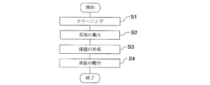
図1は成膜方法の一例を示すフローチャートである。図1を参照しながら、薄膜の形成方法を説明する。
(Embodiment 1)
FIG. 1 is a flowchart showing an example of a film forming method. A method for forming a thin film will be described with reference to FIG.
まず、基板30を反応容器10内に設置しない状態で、反応容器10のクリーニングを行う(ステップS1)。反応容器10内に、クリーニング用のプロセスガスを導入する。高周波発振電源14を作動させ、クリーニング用のプロセスガスに電界を印加して、プラズマ放電させる。プラズマ放電により活性化されたクリーニング用プロセスガスによる、プラズマガスエッチングによって、反応容器10の内壁、上部電極11、下部電極12などに付着した堆積物を除去する。クリーニング用プロセスガスには、フッ化物ガスが少なくとも用いられる。
First, the
フッ化物ガスには、OF2、ClF3、NF3、FNO、F3NO、SF6、SF5NO、SOF2などを用いることができる。 For the fluoride gas, OF 2, ClF 3, NF 3 , FNO 3 , F 3 NO 3 , SF 6, SF 5 NO , SOF 2, or the like can be used.
また、フッ化物ガスには、炭素を組成に含むフッ素化合物のガスを用いることができる。このようなフッ素化合物としては、COF2、COF2、CF3COF、CF2(COF)2、C3F7COFCF3OF、CF3I、CF3OOCF3、CF3OOOCF3、CF3CN、CF3NO、パーフルオロカーボン(例えば、CF4、C2F6、C3F8、C4F10、C3F8、C4F6、C4F8、C5F8など)、ハイドロフルオロカーボン(例えば、CF3CHF2、CHF2CHF2、CF3CHFCF3、CF3CF2CHF2、CHF2CF2CHF2など)、エーテル系フッ化物(例えば、CHF2OCHF2、CF3OCHFCF3、CF3OCF=CF2、C2F5OCF=CF2、C3F6O、C3F6O2、C4F8O、C4F8O2など)、CF3COCF3などのカルボニル系フッ化物、及び、エステル系フッ化物(例えば、CF3COOCHF2、CF3COOC2F5など)などがある。 As the fluoride gas, a fluorine compound gas containing carbon in its composition can be used. Such fluorine compounds, COF 2, COF 2, CF 3 COF, CF 2 (COF) 2, C 3 F 7 COFCF 3 OF, CF 3 I, CF 3 OOCF 3, CF 3 OOOCF 3, CF 3 CN CF 3 NO, perfluorocarbon (eg, CF 4 , C 2 F 6 , C 3 F 8 , C 4 F 10 , C 3 F 8 , C 4 F 6 , C 4 F 8 , C 5 F 8, etc.) Hydrofluorocarbons (for example, CF 3 CHF 2 , CHF 2 CHF 2 , CF 3 CHFCF 3 , CF 3 CF 2 CHF 2 , CHF 2 CF 2 CHF 2, etc.), ether fluorides (for example, CHF 2 OCHF 2 , CF 3) OCHFCF 3, CF 3 OCF = CF 2, C 2 F 5 OCF = CF 2, C 3 F 6 O, C 3 F 6 O 2, C 4 F 8 And C 4 F 8 O 2), carbonyl-based fluoride, such as CF 3 COCF 3, and, ester fluorides (e.g., such as CF 3 COOCHF 2, CF 3 COOC 2 F 5) , and the like.
フッ化物ガスの代わりに、フッ素ガス(F2ガス)を用いることもできる。 Instead of fluoride gas, fluorine gas (F 2 gas) can also be used.
フッ化物ガスをプラズマにより活性化することで、フッ素ラジカルが生成され、このフッ素ラジカルと反応容器10の内部に生成された堆積物が反応して、蒸気圧の高い揮発性のフッ化物が生成される。この間、排気口15に連結された排気手段により排気が行われ、このフッ化物は排気口15を通じて反応容器10から除去される。クリーニング用プロセスガスの供給、及び排気を停止し、クリーニングを終了する。
By activating the fluoride gas with plasma, fluorine radicals are generated, and the fluorine radicals react with the deposits generated inside the
次に、基板30を反応容器10内に搬入し、下部電極12上に設置する(ステップS2)。基板30を搬入した反応容器10内には、クリーニング用プロセスガスであるフッ化物ガスが残留し、反応容器10の内壁、上部電極11、下部電極12などに吸着している。
Next, the
次に、基板30上に薄膜を形成する、薄膜形成プロセスを行う(ステップS3)。まず、排気を行い、反応容器10内を所定の圧力にする。そして、排気を行いながら、膜を形成するための薄膜形成用プロセスガスを反応容器10内に供給し、高周波発振電源14を作動させ、薄膜形成用プロセスガスに電界を印加して、プラズマ放電させる。このプラズマ放電と同時に、反応容器10内に残留していたフッ化物ガスもプラズマ放電し、フッ素ラジカルが生成され、フッ素ラジカルが基板30に降り注ぐ状態となる。そのため、このフッ素ラジカルにより基板30の被形成面がエッチングされ、蒸気圧の高い揮発性のフッ化物が生成され、このフッ化物は排気口15から、反応容器10の外部へ除去される。
Next, a thin film formation process for forming a thin film on the
フッ素ラジカルは反応性が高いため、反応容器内にフッ素ラジカルが存在している間は、薄膜形成用プロセスガスによる膜の堆積反応ではなく、フッ素ラジカルによるエッチング反応が優位に進行する。エッチング反応の進行によりフッ素ラジカルの濃度は減少し、やがて、薄膜形成用プロセスガスに反応容器10内の雰囲気が置換され、堆積反応が開始し、基板30の被形成面に膜が成長する。よって、薄膜を形成する直前に、フッ素ラジカルによって薄膜の被形成面をプラズマガスエッチングされるため、被形成面の有機物を除去することができ、清浄な状態の被形成面に薄膜を形成することができる。
Since fluorine radicals are highly reactive, etching reactions with fluorine radicals proceed preferentially rather than film deposition reactions with a process gas for thin film formation while fluorine radicals are present in the reaction vessel. As the etching reaction proceeds, the concentration of fluorine radicals decreases, and eventually, the atmosphere in the
また、薄膜の被形成面を清浄にするプロセスと、薄膜の形成が同じ反応容器内で連続して行うことができるので、清浄にされた被形成面を大気雰囲気に曝すことなく、薄膜を形成することができる。 In addition, the process of cleaning the thin film formation surface and the thin film formation can be performed continuously in the same reaction vessel, so the thin film can be formed without exposing the cleaned formation surface to the air atmosphere. can do.
例えば、クリーニングガスにNF3を用い、基板30の被形成面に、酸化シリコン膜が形成され、この酸化シリコン膜上に、非晶質シリコン膜を形成する場合を例に、この薄膜形成プロセスを説明する。非晶質シリコン膜を形成するため、水素(H2)とモノシラン(SiH4)を薄膜形成用プロセスガスとして用いる。H2およびSiH4を反応容器10に供給し、高周波発振電源14により、H2およびSiH4に電界を印加してプラズマ放電すると、残留していた、NF3もプラズマ放電し、フッ素ラジカルが生成される。まず、このフッ素ラジカルにより、基板30の表面の酸化シリコン膜がエッチングされ、NF3が減少すると、酸化シリコン膜上に非晶質シリコンが堆積される。
For example, NF 3 is used as the cleaning gas, a silicon oxide film is formed on the surface to be formed of the
クリーニング工程で反応容器10内に残留したNF3は微量であるので、酸化シリコン膜がエッチングされる厚さは1nm未満とすることができ、例えば0.1nm以上0.5nm以下の厚さエッチングすることが可能である。そのため、薄膜形成プロセスにおいて、非晶質シリコン膜が形成される酸化シリコン膜の表面をフッ素ラジカルで清浄な状態にすることができると共に、酸化シリコン膜の厚さを微調整することが可能になる。
Since a small amount of NF 3 remains in the
もちろん、フッ素ラジカルでエッチングできる材料であれば、酸化シリコン以外の材料でもエッチングされる厚さは1nm未満とすることができ、エッチングされる厚さを0.1nm以上0.5nm以下とすることが可能である。 Of course, as long as the material can be etched with fluorine radicals, the thickness etched with a material other than silicon oxide can be less than 1 nm, and the etched thickness can be 0.1 nm or more and 0.5 nm or less. Is possible.
なお、反応容器10内のフッ化物ガスの濃度が減少する速度は、反応容器10の圧力、薄膜形成用プロセスガスの種類、流量、上部電極11及び下部電極12の温度によって変動するため、フッ素ラジカルでエッチングされる厚さに合わせて、これらの条件を適宜決定すればよい。
The rate at which the concentration of the fluoride gas in the
所定の厚さに薄膜が形成されたら、薄膜形成用プロセスガスの供給等を停止し、薄膜形成プロセスを終了する。次に、反応容器10内から、薄膜が形成された基板30を取り出す(ステップS4)。以上により、図1のプロセスフローを用いた薄膜の形成が完了する。このプロセスフローに従って薄膜を形成することで、薄膜の被形成面を清浄にするプロセスと、薄膜形成のプロセスが同じ反応容器内で連続して行われるので、清浄にされた被形成面を大気雰囲気に曝すことなく、薄膜を形成することができる。
When the thin film is formed to a predetermined thickness, the supply of the process gas for forming the thin film is stopped and the thin film forming process is terminated. Next, the
図1のプロセスフローを用いた薄膜形成方法において、薄膜形成プロセス(ステップS3)において、反応容器10内に残留しているフッ化物ガスの濃度は、クリーニングプロセス(ステップS1)が終了してから、薄膜形成プロセス(ステップS3)を開始する時間で調節することができる。
In the thin film formation method using the process flow of FIG. 1, in the thin film formation process (step S3), the concentration of the fluoride gas remaining in the
(実施の形態2)
図2は成膜方法の一例を示すフローチャートである。図2を参照しながら、薄膜の形成方法を説明する。
(Embodiment 2)
FIG. 2 is a flowchart showing an example of a film forming method. A method for forming a thin film will be described with reference to FIG.
まず、実施の形態1のステップS1と同様に、基板30を反応容器10内に設置しない状態で、反応容器10のクリーニングを行う(ステップS11)。このステップS11により、反応容器10内には、クリーニング用プロセスガスであるフッ化物ガスが残留し、反応容器10の内壁、上部電極11、下部電極12などに吸着している。次に、実施の形態のステップS2と同様に、次に、基板30を反応容器10内に搬入し、下部電極12上に設置する(ステップS12)。
First, as in step S1 of the first embodiment, the
次に、薄膜形成プロセス(ステップS14)を行う前に、反応容器10内に残留しているフッ化物ガスをプラズマ励起させ、フッ素ラジカルを発生させる。そのために、プロセスガスとして窒素ガス(N2ガス)を反応容器10に供給し、窒素ガスのプラズマを生成する(ステップS13)。
Next, before performing the thin film formation process (step S14), the fluoride gas remaining in the
まず、排気を行い、反応容器10内を所定の圧力にする。そして、排気を行いながら、窒素ガスを反応容器10内に供給し、高周波発振電源14を作動させ、窒素ガスに電界を印加して、プラズマ放電させる。窒素ガスがプラズマ放電すると共に、反応容器10内に残留していたフッ化物ガスもプラズマ放電し、フッ素ラジカルが生成される。このフッ素ラジカルにより基板30の被形成面がエッチングされ、蒸気圧の高い揮発性のフッ化物が生成され、このフッ化物は排気口15から反応容器10から除去される。
First, evacuation is performed to bring the inside of the
薄膜形成プロセス(ステップS14)を行う前に、この窒素ガスのプラズマを生成させるプロセスを行うことで、薄膜を形成する直前に、フッ素ラジカルによって薄膜の被形成面をプラズマガスエッチングされるため、被形成面の有機物を除去することができ、清浄な状態の被形成面に薄膜を形成することができる。 By performing this nitrogen gas plasma generation process before the thin film formation process (step S14), the film formation surface of the thin film is etched by fluorine radicals immediately before forming the thin film. Organic substances on the formation surface can be removed, and a thin film can be formed on a clean surface.
例えば、クリーニングガスにNF3を用い、基板30の被形成面に、酸化シリコン膜が形成されている場合を例に、この窒素ガスのプラズマの生成プロセスを説明する。窒素ガスをプラズマ励起することで、残留していたNF3もプラズマ放電し、フッ素ラジカルが生成され、このフッ素ラジカルにより、基板30表面の酸化シリコン膜がエッチングされる。クリーニングプロセス(S11)で反応容器10内に残留したNF3は微量であるので、酸化シリコン膜がエッチングされる厚さは1nm未満とすることができ、0.1nm以上0.5nm以下の範囲でエッチングすることが可能である。そのため、薄膜形成プロセスにおいて、非晶質シリコン膜が形成される酸化シリコン膜の表面をフッ素ラジカルで清浄な状態にすることができると共に、酸化シリコン膜の厚さを微調整することが可能になる。
For example, the process of generating this nitrogen gas plasma will be described by taking as an example the case where NF 3 is used as the cleaning gas and a silicon oxide film is formed on the surface of the
フッ素ラジカルでエッチングできる材料であれば、酸化シリコン以外の材料でもエッチングされる厚さは1nm未満とすることができ、エッチングされる厚さを0.1nm以上0.5nm以下とすることが可能である。 As long as the material can be etched with fluorine radicals, the thickness etched with materials other than silicon oxide can be less than 1 nm, and the etched thickness can be 0.1 nm or more and 0.5 nm or less. is there.
なお、反応容器10内のフッ化物ガスの濃度が減少する速度は、反応容器10の圧力、窒素ガスの流量、上部電極11及び下部電極12の温度によって変動するため、フッ素ラジカルでエッチングされる厚さに合わせて、これらの条件を適宜決定すればよい。
Note that the rate at which the concentration of the fluoride gas in the
また、プロセスで用いることができるプロセスガスとしては、窒素ガスの他、希ガスガス(He、Ar、Kr、Xe等)が好ましい。窒素ガス及びハロゲンガスのプラズマに含まれるラジカルは、フッ素ラジカルと反応して、揮発性のフッ化物を生成しにくいため、フッ素ラジカルの殆どを基板の被形成面において、反応させることができる。 Further, as a process gas that can be used in the process, a rare gas gas (He, Ar, Kr, Xe, etc.) is preferable in addition to nitrogen gas. Since radicals contained in the plasma of nitrogen gas and halogen gas hardly react with fluorine radicals to generate volatile fluorides, most of the fluorine radicals can be reacted on the formation surface of the substrate.
所定の期間、窒素ガスを反応容器10に供給しながら、プラズマ励起させた後、窒素ガスの供給を停止する。次に、反応容器10内に薄膜形成用プロセスガスを供給して、基板30上に薄膜を形成する、薄膜形成プロセスを行う(ステップS14)。排気を行いながら、膜を形成するための薄膜形成用プロセスガスを反応容器10内に供給し、高周波発振電源14を作動させ、薄膜形成用プロセスガスに電界を印加して、プラズマ放電させて、基板30の被形成面に薄膜を形成する。所定の厚さに薄膜が形成されたら、薄膜形成用プロセスガスの供給等を停止し、薄膜の形成プロセスを終了する。
The plasma is excited while supplying nitrogen gas to the
次に、反応容器10内から、薄膜が形成された基板30を取り出す(ステップS15)。以上により、図2のプロセスフローを用いた薄膜の形成プロセスが完了する。このプロセスフローに従って薄膜を形成することで、薄膜の被形成面を清浄にするプロセスと、薄膜形成のプロセスが同じ反応容器内で連続して行われるので、清浄にされた被形成面を大気雰囲気に曝すことなく、薄膜を形成することができる。
Next, the
図2のプロセスフローを用いた薄膜形成方法において、窒素ガスのプラズマを生成するプロセス(ステップS13)において、反応容器10内に残留しているフッ化物ガスの濃度は、クリーニングプロセス(ステップS1)が終了してから、窒素ガスのプラズマを生成するプロセス(ステップS3)を開始する時間で調節することができる。
In the thin film forming method using the process flow of FIG. 2, in the process of generating nitrogen gas plasma (step S13), the concentration of the fluoride gas remaining in the
(実施の形態3)
図3は成膜方法の一例を示すフローチャートである。図3を参照しながら、薄膜の形成方法を説明する。
(Embodiment 3)
FIG. 3 is a flowchart showing an example of a film forming method. A method for forming a thin film will be described with reference to FIG.
まず、基板30を反応容器10内に搬入し、下部電極12上に設置する(ステップS2)。
First, the
次に、フッ化物ガスを反応容器10に供給する(ステップS21)。フッ化物ガスには、NF3、SF6及びCF4から選ばれたガスを用いることができる。このうち、NF3ガスが好ましい。このとき、反応容器10の圧力は大気圧でも、大気圧よりも低くてもよい。
Next, a fluoride gas is supplied to the reaction vessel 10 (step S21). As the fluoride gas, a gas selected from NF 3 , SF 6 and CF 4 can be used. Of these, NF 3 gas is preferred. At this time, the pressure in the
次に、基板30上に薄膜を形成する、薄膜形成プロセスを行う(ステップS23)。排気を行いながら、膜を形成するための薄膜形成用プロセスガスを反応容器10内に供給し、高周波発振電源14を作動させ、薄膜形成用プロセスガスに電界を印加して、プラズマ放電させる。このプラズマ放電と同時に、ステップS21で予め供給されていたフッ化物ガスもプラズマ放電し、フッ素ラジカルが生成される。そのため、このフッ素ラジカルにより基板30の被形成面がエッチングされ、蒸気圧の高い揮発性のフッ化物が生成され、このフッ化物は排気口15から反応容器10から除去される。
Next, a thin film formation process for forming a thin film on the
フッ素ラジカルは反応性が高いため、反応容器内にフッ素ラジカルが存在している間は、薄膜形成用プロセスガスによる膜の堆積反応ではなく、フッ素ラジカルによるエッチング反応が優位に進行する。エッチング反応の進行によりフッ素ラジカルの濃度は減少し、やがて、薄膜形成用プロセスガスに反応容器10内の雰囲気が置換され、堆積反応が開始し、基板30の被形成面に膜が成長する。よって、薄膜を形成する直前に、フッ素ラジカルによって薄膜の被形成面をプラズマガスエッチングされるため、被形成面の有機物を除去することができ、清浄な状態の被形成面に薄膜を形成することができる。
Since fluorine radicals are highly reactive, etching reactions with fluorine radicals proceed preferentially rather than film deposition reactions with a process gas for thin film formation while fluorine radicals are present in the reaction vessel. As the etching reaction proceeds, the concentration of fluorine radicals decreases, and eventually, the atmosphere in the
例えば、クリーニングガスにNF3を用い、基板30の被形成面に、酸化シリコン膜が形成され、この酸化シリコン膜上に、非晶質シリコン膜を形成する場合を例に、この薄膜形成プロセスを説明する。非晶質シリコン膜を形成するため、水素(H2)とモノシラン(SiH4)を薄膜形成用プロセスガスとして用いる。H2およびSiH4を反応容器10に供給し、高周波発振電源14により、H2およびSiH4に電界を印加してプラズマ放電すると、NF3もプラズマ放電し、フッ素ラジカルが生成される。まず、このフッ素ラジカルにより、基板30の表面の酸化シリコン膜がエッチングされ、次いで、NF3が減少すると、酸化シリコン膜上に非晶質シリコンが堆積される。
For example, NF 3 is used as the cleaning gas, a silicon oxide film is formed on the surface to be formed of the
ステップS22で反応容器10に供給するフッ化物ガスの量を調節することで、酸化シリコン膜がエッチングされる厚さは1nm未満とすることができ、0.1nm以上0.5nm以下の範囲でエッチングすることが可能である。そのため、非晶質シリコン膜が形成される酸化シリコン膜の表面をフッ素ラジカルで清浄な状態にすることができると共に、酸化シリコン膜の厚さを微調整することが可能になる。もちろん、フッ素ラジカルでエッチングできる材料であれば、酸化シリコン以外の材料でもエッチングされる厚さは1nm未満とすることができ、エッチングされる厚さを0.1nm以上0.5nm以下とすることが可能である。なお、フッ化物ガスの量の調節は、フッ化物ガスの流量、排気量を調節することで可能である。
By adjusting the amount of the fluoride gas supplied to the
所定の厚さに薄膜が形成されたら、薄膜形成用プロセスガスの供給を停止し、また排気を停止し、薄膜形成プロセスを終了する。薄膜の被形成面を清浄にするプロセスと、薄膜形成のプロセスが同じ反応容器内で連続して行われるので、清浄にされた被形成面を大気雰囲気に曝すことなく、薄膜を形成することができる。 When the thin film is formed to a predetermined thickness, the supply of the process gas for forming the thin film is stopped, the exhaust is stopped, and the thin film forming process is finished. Since the process of cleaning the thin film forming surface and the process of forming the thin film are continuously performed in the same reaction vessel, the thin film can be formed without exposing the cleaned film forming surface to the air atmosphere. it can.
次に、反応容器10内から、薄膜が形成された基板30を取り出す(ステップS24)。以上により、図3のプロセスフローを用いた薄膜の形成が完了する。
Next, the
図3のプロセスフローを用いた薄膜形成方法では、クリーニングプロセスの後に、薄膜形成のプロセスを行わない場合でも、薄膜形成のプロセス(ステップS23)において、薄膜の被形成面をフッ素ラジカルによるプラズマガスエッチングすることができる。 In the thin film formation method using the process flow of FIG. 3, even if the thin film formation process is not performed after the cleaning process, the thin film formation surface (plasma gas etching with fluorine radicals) is performed in the thin film formation process (step S23). can do.
(実施の形態4)
図4は成膜方法の一例を示すフローチャートである。図4を参照しながら、薄膜の形成方法を説明する。
(Embodiment 4)
FIG. 4 is a flowchart showing an example of a film forming method. A method for forming a thin film will be described with reference to FIG.
まず、基板30を反応容器10内に搬入し、下部電極12上に設置する(ステップS31)。次に、図3のステップS22と同様に、フッ化物ガスを反応容器10に供給する(ステップS32)
First, the
次に、ステップS32で反応容器10内に供給したフッ化物ガスをプラズマ励起させ、フッ素ラジカルを発生させる。そのために、プロセスガスとして、窒素ガス(N2ガス)を反応容器10に供給し、窒素ガスのプラズマを生成する(ステップS33)。このプロセスは、図2のステップS13と同様に行うことができる。
Next, the fluoride gas supplied into the
薄膜形成プロセス(ステップS34)を行う前に、この窒素ガスのプラズマを生成させるプロセスを行うことで、薄膜を形成する直前に、フッ素ラジカルによって薄膜の被形成面をプラズマガスエッチングされるため、被形成面の有機物を除去することができ、清浄な状態の被形成面に薄膜を形成することができる。 By performing the process of generating the nitrogen gas plasma before the thin film formation process (step S34), the film formation surface of the thin film is plasma-etched by fluorine radicals immediately before the thin film is formed. Organic substances on the formation surface can be removed, and a thin film can be formed on a clean surface.
例えば、クリーニングガスにNF3を用い、基板30の被形成面に、酸化シリコン膜が形成されている場合を例に、この窒素ガスのプラズマの生成プロセスを説明する。窒素ガスをプラズマ励起することで、予め供給されていたNF3もプラズマ放電し、フッ素ラジカルが生成される。このフッ素ラジカルにより、基板30の表面の酸化シリコン膜がエッチングされる。
For example, the process of generating this nitrogen gas plasma will be described by taking as an example the case where NF 3 is used as the cleaning gas and a silicon oxide film is formed on the surface of the
ステップS32で反応容器10に供給するフッ化物ガスの量を調節することで、酸化シリコン膜がエッチングされる厚さは1nm未満とすることができ、0.1nm以上0.5nm以下の範囲でエッチングすることが可能である。そのため、非晶質シリコン膜が形成される酸化シリコン膜の表面をフッ素ラジカルで清浄な状態にすることができると共に、酸化シリコン膜の厚さを微調整することが可能になる。もちろん、フッ素ラジカルでエッチングできる材料であれば、酸化シリコン以外の材料でもエッチングされる厚さは1nm未満とすることができ、エッチングされる厚さを0.1nm以上0.5nm以下とすることが可能である。なお、フッ化物ガスの量の調節は、フッ化物ガスの流量、排気量を調節することで可能である。
By adjusting the amount of fluoride gas supplied to the
このプロセスで用いることができるプロセスガスとしては、窒素ガスの他、希ガスガス(He、Ar、Kr、Xe等)が好ましい。窒素ガス及びハロゲンガスのプラズマに含まれるラジカルは、フッ素ラジカルと反応して、揮発性のフッ化物を生成しにくいため、フッ素ラジカルの殆どを基板の被形成面において、反応させることができる。 As a process gas that can be used in this process, a rare gas gas (He, Ar, Kr, Xe, etc.) is preferable in addition to nitrogen gas. Since radicals contained in the plasma of nitrogen gas and halogen gas hardly react with fluorine radicals to generate volatile fluorides, most of the fluorine radicals can be reacted on the formation surface of the substrate.
次に、窒素ガスの供給を停止し、基板30上に薄膜を形成する、薄膜形成プロセスを行う(ステップS34)。排気を行いながら、膜を形成するための薄膜形成用プロセスガスを反応容器10内に供給し、高周波発振電源14を作動させ、薄膜形成用プロセスガスに電界を印加して、プラズマ放電させて、基板30の被形成面に薄膜を形成する。定の厚さに薄膜が形成されたら、薄膜形成用プロセスガスの供給等を停止し、薄膜形成プロセスを終了する。
Next, the supply of nitrogen gas is stopped, and a thin film formation process is performed to form a thin film on the substrate 30 (step S34). While evacuating, a thin film forming process gas for forming a film is supplied into the
次に、反応容器10内から、薄膜が形成された基板30を取り出す(ステップS35)。以上により、図3のプロセスフローを用いた薄膜の形成が完了する。本実施の形態の成膜方法は、薄膜の被形成面を清浄にするプロセスと、薄膜形成のプロセスが同じ反応容器内で連続して行われるので、清浄にされた被形成面を大気雰囲気に曝すことなく、薄膜を形成することができる。
Next, the
図4のプロセスフローを用いた薄膜形成方法では、クリーニングプロセスの後に、薄膜形成のプロセスを行わない場合でも、薄膜形成のプロセス(ステップS23)において、薄膜の被形成面をフッ素ラジカルによるプラズマガスエッチングすることができる。 In the thin film formation method using the process flow of FIG. 4, even if the thin film formation process is not performed after the cleaning process, in the thin film formation process (step S23), the surface on which the thin film is formed is plasma gas etched by fluorine radicals. can do.
(実施の形態5)
実施の形態1乃至実施の形態4の薄膜の形成プロセスを用いることで、各種の素子を有する半導体装置を形成することができる。本発明者は、実験により反応容器10内に存在するフッ化物ガスにより被形成面がごくわずかにエッチングされることを確認した。本実施の形態では、その実験について説明する。この実験では、図4のプロセスフローを用いてステップS31〜ステップS34までプロセスを行い、フッ化物ガスによって薄膜がエッチングされる厚さを測定した。以下、実験方法を説明する。
(Embodiment 5)
By using the thin film formation process of Embodiments 1 to 4, a semiconductor device having various elements can be formed. The inventor has confirmed by experiments that the surface to be formed is etched very slightly by the fluoride gas present in the
基板30として、ガラス基板を用いた。反応容器10内に基板30を搬入し、ガラス基板上に、図5に示す容量結合PECVD装置を用いて、非晶質シリコン膜を形成した。厚さが55nmになるように成膜時間を調節した。非晶質シリコン膜の形成プロセスの条件を以下に示す。
・プロセスガスの種類(流量)
SiH4(25sccm)
H2(150sccm)
・下部電極温度 250℃
・圧力 66.7Pa
・高周波発振電源の発振周波数 27MHz
・高周波電源の出力電力 50W
・電極間距離 25mm
・電極面積 615.75cm2
A glass substrate was used as the
・ Process gas type (flow rate)
SiH 4 (25 sccm)
H 2 (150 sccm)
・ Lower electrode temperature 250 ℃
・ Pressure 66.7Pa
・ Oscillation frequency of high-frequency oscillation power supply 27MHz
・ Output power of high frequency power supply 50W
・ Distance between electrodes 25mm
-Electrode area 615.75 cm 2
フッ化物ガスによってエッチングされる厚さを測定するため、反応容器10から非晶質シリコン膜が形成された基板30を搬出し、非晶質シリコン膜の厚さを測定した。
In order to measure the thickness etched by the fluoride gas, the
次に、非晶質シリコン膜が形成された基板30を反応容器10に搬入した。内蔵されたヒータにより上部電極11、および下部電極12の温度を200℃に上昇させ、流量200sccmの流量で、60秒間、NF3ガスを反応容器10に供給した。排気手段である真空ポンプを動作させ、排気を行いながら、NF3ガスを供給した。NF3ガスが供給された反応容器10内の圧力は、1.5Pa程度である。
Next, the
次に、排気手段である真空ポンプを動作させながら、窒素ガスを反応容器10に供給し、窒素ガスのプラズマを生成させ、フッ素ラジカルにより基板30に形成された非晶質シリコン膜をエッチングした。窒素ガスのプラズマ処理プロセスの条件を以下に示す。
・プロセスガスの種類(流量)
N2(200sccm)
・上部電極温度 200℃
・下部電極温度 200℃
・圧力 40Pa
・高周波発振電源の発振周波数 13.56MHz
・高周波発振電源の出力電力 50W
・電極間距離 20mm
・電極面積 651.44cm2
Next, nitrogen gas was supplied to the
・ Process gas type (flow rate)
N 2 (200 sccm)
・
・
・ Pressure 40Pa
・ Oscillation frequency of high-frequency oscillation power supply 13.56MHz
・ High frequency oscillation power supply output power 50W
・ Distance between electrodes 20mm
-Electrode area 651.44 cm 2
窒素ガスによるプラズマ処理時間を変化させて、非晶質シリコン膜の厚さの変化を測定した。図6に測定結果を示す。図6は、窒素ガスのプラズマ処理時間に対する、非晶質膜の厚さの変化を示す散布図である。プラズマ処理時間は、5秒、10秒、15秒、20秒、25秒とした。非晶質シリコン膜の厚さの変化は、窒素ガスのプラズマ処理前と後での非晶質シリコン膜の厚さの差分である。非晶質シリコン膜の厚さは膜厚測定装置で計測した。用いた測定装置の精度は0.1nmである。また、非晶質シリコン膜の厚さは、100mm×100mmの矩形の領域で25箇所測定した。 The change in the thickness of the amorphous silicon film was measured by changing the plasma treatment time with nitrogen gas. FIG. 6 shows the measurement results. FIG. 6 is a scatter diagram showing changes in the thickness of the amorphous film with respect to the plasma treatment time of nitrogen gas. The plasma treatment time was 5 seconds, 10 seconds, 15 seconds, 20 seconds, and 25 seconds. The change in the thickness of the amorphous silicon film is the difference between the thickness of the amorphous silicon film before and after the plasma treatment with nitrogen gas. The thickness of the amorphous silicon film was measured with a film thickness measuring device. The accuracy of the measurement apparatus used is 0.1 nm. Further, the thickness of the amorphous silicon film was measured at 25 points in a rectangular region of 100 mm × 100 mm.
図6に示すように、窒素ガスのプラズマ処理によって、NF3ガスにより、非晶質シリコン膜がエッチングされていることが分かる。また、非晶質シリコン膜を0.5nm以下の厚さ範囲で、より具体的には、0.1nm〜エッチングすることが可能になる。図6の結果は、反応容器10内のNF3ガス濃度を調節することで、非晶質シリコン膜がエッチングされる厚さを調節できることを示している。
As shown in FIG. 6, it can be seen that the amorphous silicon film is etched by NF 3 gas by the nitrogen gas plasma treatment. In addition, the amorphous silicon film can be etched in a thickness range of 0.5 nm or less, more specifically from 0.1 nm. The result of FIG. 6 shows that the thickness at which the amorphous silicon film is etched can be adjusted by adjusting the NF 3 gas concentration in the
よって、図1〜図4に示す薄膜の成膜において、薄膜の形成前に反応容器10にフッ化物ガスを供給し、他のプロセスガスによるプラズマ処理によって、フッ素ラジカルを発生させることで、基板30上に形成されている薄膜、又は基板30を0.1nm単位でエッチングすることが可能である。例えば、薄膜または基板30を0.1nm以上0.5nm以下の範囲でエッチングすることが可能である。
Accordingly, in forming the thin film shown in FIGS. 1 to 4, the fluoride gas is supplied to the
(実施の形態6)
本実施の形態では、半導体装置の作製方法の一例として、不揮発性半導体記憶装置の作製について説明する。
(Embodiment 6)
In this embodiment, manufacturing of a nonvolatile semiconductor memory device will be described as an example of a method for manufacturing a semiconductor device.
図7は、不揮発性半導体記憶装置の構成例を示すブロック図である。図7の不揮発性半導体記憶装置は、メモリセルアレイ52と、メモリセルアレイ52に接続され、書き込み動作、消去動作および読み出し動作などを制御するロジック部54が同一の基板上に形成されている。メモリセルアレイ52は、複数のワード線WLと、ワード線WLと交差して形成された複数のビット線BL、およびワード線WL及びビット線BLに接続された複数のメモリセルMCを有する。メモリセルMCのデータの蓄積手段として、実施の形態1で説明した不揮発性メモリトランジスタが用いられる。そのため、電荷保持特性に優れ、信頼性の高い不揮発性半導体記憶装置を得ることができる。
FIG. 7 is a block diagram illustrating a configuration example of the nonvolatile semiconductor memory device. The nonvolatile semiconductor memory device of FIG. 7 includes a
ロジック部54の構成は以下の通りである。ワード線選択のためにロウデコーダ62と、ビット線選択のためにカラムデコーダ64が、メモリセルアレイ52の周囲に設けられている。アドレスは、アドレスバッファ56を介してコントロール回路58に送られ、内部ロウアドレス信号及び内部カラムアドレス信号がそれぞれロウデコーダ62及びカラムデコーダ64に転送される。
The configuration of the
データ書き込み及び消去には、電源電位を昇圧した電位が用いられる。このため、コントロール回路58により動作モードに応じて制御される昇圧回路60が設けられている。昇圧回路60の出力はロウデコーダ62やカラムデコーダ64を介して、メモリセルアレイ52に形成されているワード線Wやビット線BLに供給される。センスアンプ66はカラムデコーダ64から出力されたデータが入力される。センスアンプ66により読み出されたデータは、データバッファ68に保持され、コントロール回路58からの制御により、データがランダムアクセスされ、データ入出力バッファ70を介して出力されるようになっている。書き込みデータは、データ入出力バッファ70を介してデータバッファ68に一旦保持され、コントロール回路58の制御によりカラムデコーダ64に転送される。
For writing and erasing data, a potential obtained by boosting the power supply potential is used. Therefore, a
図8は、メモリセルアレイ52の構成例を示す回路図である。メモリセルMCが行列状に配置されている。図8では、3行×2列のメモリセルMCを示している。各メモリセルMCは1ビットの情報を記憶し、直列に接続されたスイッチング用トランジスタTs、不揮発性メモリメモリトランジスタTmを有する。メモリセルアレイ52は、列ごとに、ビット線BL0、BL1、ソース線SL0、SL1が設けられている。また、行ごとに、第1ワード線WL1〜WL3及び第2ワード線WL11〜WL13が設けられている。
FIG. 8 is a circuit diagram illustrating a configuration example of the
ビット線BL0及び第1ワード線WL1で特定されるメモリセルMCに着目すると、スイッチング用トランジスタTsは、ゲートが第2ワード線WL11に接続され、ソースまたはドレインの一方がビット線BL0に接続され、他方が不揮発性メモリトランジスタTmに接続されている。不揮発性メモリトランジスタTmは、ゲートが第1ワード線WL1に接続され、ソースまたはドレインの一方がスイッチング用トランジスタTsに接続され、他方がソース線SL0に接続されている。 Focusing on the memory cell MC specified by the bit line BL0 and the first word line WL1, the switching transistor Ts has a gate connected to the second word line WL11 and one of the source and drain connected to the bit line BL0. The other is connected to the nonvolatile memory transistor Tm. The nonvolatile memory transistor Tm has a gate connected to the first word line WL1, one of a source and a drain connected to the switching transistor Ts, and the other connected to the source line SL0.
スイッチング用トランジスタTsと不揮発性メモリメモリトランジスタTmを共にnチャネル型とした場合、ビット線BL0及び第1ワード線WL1で特定されるメモリセルMCにデータを書き込むには、第2ワード線W11とビット線BL0の電位をHレベル、ビット線BL1の電位をLレベルとして、第2ワード線W11に高電圧を印加する。これにより、不揮発性メモリメモリトランジスタTmの電荷蓄積層に電荷が注入される。不揮発性メモリメモリトランジスタTmからデータを消去するには、第1ワード線W1及びビット線BL0の電位をHレベルとし、第2ワード線W11に負の高電圧を印加する。 When both the switching transistor Ts and the nonvolatile memory memory transistor Tm are n-channel type, in order to write data to the memory cell MC specified by the bit line BL0 and the first word line WL1, the second word line W11 and the bit A high voltage is applied to the second word line W11 by setting the potential of the line BL0 to the H level and the potential of the bit line BL1 to the L level. As a result, charges are injected into the charge storage layer of the nonvolatile memory memory transistor Tm. In order to erase data from the nonvolatile memory transistor Tm, the potentials of the first word line W1 and the bit line BL0 are set to H level, and a negative high voltage is applied to the second word line W11.
次に、図9〜図15を用いて、不揮発性半導体記憶装置の作製方法について説明する。 Next, a method for manufacturing a nonvolatile semiconductor memory device will be described with reference to FIGS.
不揮発性半導体記憶装置において、メモリセルアレイのトランジスタは、ロジック部のトランジスタと比較して駆動電圧が高いため、メモリセルアレイのトランジスタとロジック部のトランジスタは、それぞれ、駆動電圧によって構造を変えることが好ましい。例えば、駆動電圧が小さく、しきい値電圧値のばらつきを小さくしたい場合にはゲート絶縁膜を薄くすることが好ましい。駆動電圧が大きくゲート絶縁膜の絶縁耐圧性が求められる場合にはゲート絶縁膜を厚くすることが好ましい。 In the nonvolatile semiconductor memory device, the transistors in the memory cell array have a higher driving voltage than the transistors in the logic portion. Therefore, the transistors in the memory cell array and the transistors in the logic portion preferably have different structures depending on the driving voltage. For example, when the driving voltage is small and it is desired to reduce variation in threshold voltage value, it is preferable to make the gate insulating film thin. When the driving voltage is large and the dielectric strength of the gate insulating film is required, it is preferable to increase the thickness of the gate insulating film.
そこで、本実施の形態では、ゲート絶縁膜の厚さが異なるトランジスタを同一基板上に作製する方法を説明する。また、本実施の形態では、トランジスタおよび不揮発性メモリトランジスタを薄膜トランジスタで作製する方法を説明する。また、本実施の形態では、不揮発性半導体記憶装置として図7の装置を例に、またそのメモリセルアレイ52を図8に示す回路で構成した場合を例に、不揮発性半導体装置の作製方法を説明する。後述する実施の形態4乃至8の不揮発性半導体記憶装置もこの点は同様である。
Thus, in this embodiment, a method for manufacturing transistors with different gate insulating film thickness over the same substrate is described. In this embodiment, a method for manufacturing a transistor and a nonvolatile memory transistor with thin film transistors will be described. Further, in this embodiment mode, a method for manufacturing a nonvolatile semiconductor device will be described by using the device in FIG. 7 as an example of a nonvolatile semiconductor memory device and an example in which the
図9〜図12は、本実施の形態の作製工程を説明するための断面図である。図9〜図12において、A−B間にロジック部54に設けられるpチャネル型トランジスタTrpの断面を示し、及びC−D間にロジック部54に設けられるnチャネル型トランジスタTrnの断面を示す。また、E−F間にメモリセルMCに設けられる不揮発性メモリトランジスタTmの断面を示し、G−H間にメモリセルMCのスイッチング用トランジスタTsの断面を示す。また、図13〜15は、本実施の形態の作製工程を説明するための上面図である。図13〜図15の一点鎖線A−B、C−D、E−F及びG−Hで切った断面図が、図9〜図12に対応する。
9 to 12 are cross-sectional views for explaining a manufacturing process of this embodiment mode. 9 to 12, a cross section of the p-channel transistor Trp provided in the
まず、図9(A)に示すように、基板100上に下地絶縁膜102を形成する。基板100は、ガラス基板、石英基板、金属基板(例えばセラミック基板またはステンレス基板など)を用いることができる。下地絶縁膜102は、CVD法やスパッタ法等を用いて、酸化シリコン、窒化シリコン、酸化窒化シリコン等の絶縁材料を用いて形成することができる。例えば、下地絶縁膜102を2層構造とする場合、第1層目の絶縁層として酸化窒化シリコン層を形成し、第2層目の絶縁層として酸化窒化シリコン層を形成するとよい。また、第1層目の絶縁層として窒化シリコン層を形成し、第2層目の絶縁層として酸化シリコン層を形成してもよい。このように、ブロッキング層として機能する下地絶縁膜102を形成することによって、基板100からNaなどのアルカリ金属やアルカリ土類金属が、この上に形成する素子に悪影響を与えることを防ぐことができる。
First, as illustrated in FIG. 9A, the
次に、下地絶縁膜102上に、島状の半導体膜104、106、108、110を形成する。図13が島状の半導体膜104、106、108、110の上面図である。島状の半導体膜104、106、108、110の形成は、次の通りに行うことができる。スパッタ法、LPCVD法、PECVD法等を用いて、シリコン(Si)を主成分とする非晶質半導体膜を形成し、非晶質半導体膜を結晶化させて、結晶性半導体膜を形成する。結晶性半導体膜をエッチングして、島状の半導体膜104、106、108、110を形成する。なお、非晶質半導体膜として、非晶質シリコン膜、非晶質ゲルマニウムまたは非晶質シリコンゲルマニウム膜などを形成することができる。また非晶質半導体膜の結晶化は、レーザ結晶化法、RTA又はファーネスアニール炉を用いる熱結晶化法、結晶化を助長する金属元素を用いる熱結晶化法またはこれら方法を組み合わせた方法等により行うことができる。
Next, island-shaped
また、基板100として、SOI基板を用いることもできる。この場合、SOI基板の半導体層を、エッチングして、島状の半導体膜104、106、108、110を形成することができる。また、半導体層を部分的に酸化して、酸化させない領域を島状の半導体膜104、106、108、110とすることができる。SOI基板の代わりに、GOI基板、SGOI基板を用いることもできる。
Alternatively, an SOI substrate can be used as the
次に、図9(A)に示すように、島状の半導体膜104、106、108、110を覆うように絶縁膜112を形成する。絶縁膜112は、LPCVD法、PECVD法により、酸化シリコン、窒化シリコン、酸化窒化シリコンでなる単層膜または2層以上の多層膜で形成される。絶縁膜112は、メモリセルMCのトランジスタTsのゲート絶縁膜として機能する。そのため、10nm〜50nmの厚さに形成される。
Next, as illustrated in FIG. 9A, an insulating
次に、図9(B)に示すように、絶縁膜112を選択的に除去し、半導体膜104、106、108の表面を露出させる。ここでは、メモリ部に設けられた半導体膜110を選択的にレジスト114で覆い、半導体膜104、106、108上に形成された、絶縁膜112をエッチングすることによって除去する。
Next, as illustrated in FIG. 9B, the insulating
レジスト114を除去し、図9(C)に示すように、半導体膜104、106、108上に絶縁膜116、118、120をそれぞれ形成する。絶縁膜116、118、120の厚さは、1〜10nmが好ましく、1〜5nmがより好ましい。なお、絶縁膜116、及び118は後の工程で除去される。
The resist 114 is removed, and as shown in FIG. 9C, insulating
絶縁膜116、118、120は、半導体膜104、106、108を熱処理又は高密度プラズマ処理等によって形成することができる。ここでは、まず、反応容器内に酸素(O2)とアルゴン(Ar)との混合ガスを導入し、高密度プラズマにより酸素ラジカルを発生させて、半導体膜104、106、108に酸化処理を行い、半導体膜104、106、108の表面に3nm〜6nm程度の厚さの酸化シリコン層を形成する。プロセスガスの流量は、酸素は0.1〜100sccm、アルゴンは100〜5000sccmとすることができる。
The insulating
続けて、酸化処理を行った反応容器内に、窒素(N2)とアルゴン(Ar)との混合ガスを導入し、高密度プラズマにより窒素ラジカルを発生させて、酸化シリコン層を窒化処理する。例えば、窒化処理時間を調節することで、窒素濃度が20〜50atomic%程度の厚さ1nm程度の層を酸化シリコン層に形成することができる。また、この際に、半導体膜110上に形成された絶縁膜112の表面も酸化又は窒化され、酸化窒化シリコン層が形成される場合がある。プロセスの流量は、窒素は20〜2000sccm、アルゴンは100〜10000sccmとすることができる。
Subsequently, a mixed gas of nitrogen (N 2 ) and argon (Ar) is introduced into the reaction vessel that has been subjected to the oxidation treatment, and nitrogen radicals are generated by high-density plasma to nitride the silicon oxide layer. For example, by adjusting the nitriding time, a layer with a nitrogen concentration of about 20 to 50 atomic% and a thickness of about 1 nm can be formed in the silicon oxide layer. At this time, the surface of the insulating
次に、図10(A)に示すように、絶縁膜112、絶縁膜116、118、120を覆うように電荷蓄積層122を形成する。例えば、電荷蓄積層122の形成に実施の形態1乃至4で説明した薄膜の形成方法を用いることができる。ここでは、実施の形態1の薄膜形成方法を適用する。まず、NF3ガスを用いて図5のPECVD装置の反応容器10をクリーニングする。そして、図9(C)の状態の基板100を反応容器10に搬入する。薄膜形成用プロセスガスとして、NH3及びSiH4を反応容器10に供給し、電荷蓄積層122として窒化シリコン膜を形成する。NH3及びSiH4がプラズマ励起されると、反応容器10に存在しているNF3もプラズマ化され、フッ素ラジカルが基板100に降り注ぐ。この結果、絶縁膜112、116、118、120がわずかにエッチングされる。絶縁膜120を薄くすることができることから、メモリトランジスタTmへの書き込み特性または読み出し特性を向上させることができる。
Next, as illustrated in FIG. 10A, the
次に、図10(B)に示すように、レジスト124を形成し、エッチングにより絶縁膜116、118、電荷蓄積層122を部分的に除去して、半導体膜104、106の上面および、半導体膜108上の絶縁膜120上面を露出させ、メモリトランジスタTmとなる半導体膜108上に電荷蓄積層122を残す。
Next, as shown in FIG. 10B, a resist 124 is formed, and the insulating
レジスト124を除去し、図10(C)に示すように基板100上に絶縁膜128を形成する。絶縁膜128は、CVD法やスパッタ法等を用いて、酸化シリコン、窒化シリコン、酸化窒化シリコン等でなる絶縁材料を堆積することで、形成される。絶縁膜128は単層膜又は2層以上の多層膜で形成される。例えば、絶縁膜128を単層で設ける場合には、CVD法により酸化窒化シリコン層を5〜50nmの厚さで形成する。また、絶縁膜128を3層構造で設ける場合には、第1層目の絶縁層として酸化窒化シリコン層を形成し、絶縁膜として窒化シリコン層を形成し、第3の絶縁層として酸化窒化シリコン層を形成する。なお、絶縁膜128をPECVD法で形成する場合は、実施の形態1乃至4の薄膜の形成方法を用いることができる。
The resist 124 is removed, and an insulating
次に、図11(A)に示すように、絶縁膜128上に導電膜130を形成し、導電膜130上に導電膜132を形成する。導電膜130と導電膜132でなる積層膜は、トランジスタTrp、Trn、TsおよびメモリトランジスタTmのゲート電極を構成する。例を示している。もちろん、ゲート電極は単層構造の導電膜で形成することができる。
Next, as illustrated in FIG. 11A, the
なお、メモリトランジスタTmをMNOS型とする場合は、導電膜130を形成する工程の前に、エッチングを行って、メモリトランジスタTmが形成される領域から絶縁膜128を除去する。
Note that in the case where the memory transistor Tm is an MNOS type, etching is performed before the step of forming the
導電膜130、132は単層構造または2層以上の多層構造とすることができる。導電膜130、132を構成する導電性材料には、タンタル(Ta)、タングステン(W)、チタン(Ti)、モリブデン(Mo)、アルミニウム(Al)、銅(Cu)、クロム(Cr)、ニオブ(Nb)等から選択された単体金属、これらの金属を主成分とする合金、及び化合物材料、並びにリン等の不純物元素をドーピングした多結晶シリコン等を用いることができる。例えば金属化合物としては、金属窒化物、シリサイド等がある。
The
例えば、導電膜130を窒化タンタル膜で形成し、導電膜132をタングステン膜で形成する。また、導電膜130を窒化タングステン、窒化モリブデン又は窒化チタンから選ばれた導電材料の単層膜又は積層膜で形成し、導電膜132を、タンタル、モリブデン、チタンから選ばれた導電材料の単層膜は積層膜で形成することができる。
For example, the
次に、図11(B)に示すように、導電膜130、132でなる積層膜をエッチングして、半導体膜104、106、108、110に重なる導電膜134、136、138、140を形成する。この状態の上面図が図14である。
Next, as illustrated in FIG. 11B, the stacked film including the
次に、図11(C)に示すように、半導体膜104を覆うレジスト142を選択的に形成する。導電膜136、138、140をマスクとして半導体膜106、108、110にn型不純物を添加し、n型の高濃度不純物領域146、150、154を形成する。高濃度不純物領域146、150、154は、ソース領域又はドレイン領域を構成する。このn型不純物の添加により、半導体膜106、108、110に、チャネル形成領域144、148、152が自己整合的に形成される。
Next, as illustrated in FIG. 11C, a resist 142 that covers the
レジスト142を除去する。次に、図12(A)に示すように、レジスト156、半導体膜106、108、110を覆うレジスト156を形成する。導電膜134をマスクとして半導体膜104、108、110にp型不純物を添加し、p型の高濃度不純物領域160を形成する。高濃度不純物領域160は、ソース領域又はドレイン領域を構成する。このp型不純物の添加により、半導体膜104に、チャネル形成領域158が自己整合的に形成される。
The resist 142 is removed. Next, as illustrated in FIG. 12A, a resist 156 that covers the resist 156 and the
レジスト156を除去する。次に、図12(B)に示すように、導電膜134、136、138、140を覆うように絶縁膜162を形成する。絶縁膜162に、高濃度不純物領域146、150、154、160に達する開口部を形成する。絶縁膜162上に半導体膜104、106、108、110にそれぞれ形成された高濃度不純物領域146、150、154、160に電気的に接続する導電膜164を形成する。この状態の上面図が図15である。
The resist 156 is removed. Next, as illustrated in FIG. 12B, an insulating
絶縁膜162は単層構造または積層構造とすることができる。絶縁膜162を構成する絶縁膜として、CVD法やスパッタ法等により、酸化シリコン、窒化シリコン、酸化窒化シリコン、DLC(ダイヤモンドライクカーボン)等の無機絶縁膜で形成することができる。また、エポキシ、ポリイミド、ポリアミド、ポリビニルフェノール、ベンゾシクロブテン、アクリル等の有機材料でなる膜、シロキサン樹脂等のシロキサン材料からなる膜を用いることができる。
The insulating
導電膜164は単層構造または積層構造とすることができる。導電膜164を構成する導電性材料には、CVD法やスパッタ法等により、アルミニウム(Al)、タングステン(W)、チタン(Ti)、タンタル(Ta)、モリブデン(Mo)、ニッケル(Ni)、白金(Pt)、銅(Cu)、金(Au)、銀(Ag)、マンガン(Mn)、ネオジウム(Nd)から選択された単体金属元素、又はこれらの元素を主成分とする合金材料若しくは化合物材料を用いることができる。例えば、アルミニウムを主成分とする合金材料とは、例えば、アルミニウムとニッケルの合金、ニッケルと、炭素とシリコンの一方又は両方とを含むアルミニウム合金などがある。アルミニウムやアルミニウムシリコンは抵抗値が低く、安価であるため、導電膜164を形成する材料に適している。
The
例えば、3層構造の導電膜164として、バリア層とアルミニウムシリコン(Al−Si)層とバリア層の積層膜、バリア層とアルミニウムシリコン(Al−Si)層と窒化チタン(TiNx)層とバリア層の積層膜などがある。なお、バリア層は、チタン、チタンの窒化物、モリブデン、又はモリブデンの窒化物からなる薄膜で形成される。上層と下層のバリア層を設けると、アルミニウムやアルミニウムシリコンのヒロックの発生を防止することができる。また、還元性の高い元素であるチタンからなるバリア層を形成すると、結晶質半導体層上に薄い自然酸化膜ができていたとしても、この自然酸化膜を還元し、結晶質半導体層と良好なコンタクトをとることができる。
For example, as the
以上の工程により、メモリセルアレイ52およびロジック部54を同一基板100上に集積された不揮発性半導体装置を作製することができる。
Through the above steps, a nonvolatile semiconductor device in which the
(実施の形態7)
ガラス基板上にTFT(thin film transistor 以下、「TFT」という。)を用いて集積回路を形成するために、ガラス基板上に、単結晶シリコンを形成することを目標に結晶化技術が研究されている。本出願人の研究した、結晶化技術として、ニッケルなどの金属元素を非晶質シリコン膜に添加してシリコンを結晶化させる技術を開発している。この結晶化技術では、金属元素がいわば触媒となり結晶化を促進し、また、結晶化に必要とされる温度を低下させる効果を利用している。金属元素を用いることで、結晶化されたシリコンの結晶方位の配向性を高めることも可能となっている。このような触媒作用のある金属元素としてはFe、Ni、Co、Ru、Rh、Pd、Os、Ir、Pt、Cu、Auから選ばれた一種または複数種であることが知られている。
(Embodiment 7)
In order to form an integrated circuit using a TFT (Thin Film Transistor, hereinafter referred to as “TFT”) on a glass substrate, a crystallization technique has been studied with the goal of forming single crystal silicon on the glass substrate. Yes. As a crystallization technique studied by the present applicant, a technique for crystallizing silicon by adding a metal element such as nickel to an amorphous silicon film has been developed. In this crystallization technique, a metal element acts as a catalyst to promote crystallization, and utilizes the effect of lowering the temperature required for crystallization. By using a metal element, it is possible to enhance the crystal orientation of crystallized silicon. It is known that such a catalytic metal element is one or more selected from Fe, Ni, Co, Ru, Rh, Pd, Os, Ir, Pt, Cu, and Au.
しかしながら、金属元素は、電気的特性のばらつき、リーク電流の増加などTFTの信頼性を低下させる要因であり、金属元素は、結晶性シリコン膜が形成されてしまえば、不要な存在となる。そこで、本出願人は、金属元素非晶質シリコン膜から除去するゲッタリング技術も開発している。そのゲッタリング技術の1つは、希ガス元素を含む半導体膜をゲッタリングサイトとして用いるゲッタリング技術である。 However, the metal element is a factor that lowers the reliability of the TFT, such as variations in electrical characteristics and an increase in leakage current, and the metal element becomes unnecessary once the crystalline silicon film is formed. Therefore, the present applicant has also developed a gettering technique for removing the metal element from the amorphous silicon film. One of the gettering techniques is a gettering technique using a semiconductor film containing a rare gas element as a gettering site.
図16を用いて、希ガス元素を含む半導体膜をゲッタリングサイトとして用いるゲッタリングプロセスを含んだ半導体装置の作製方法を説明する。 A method for manufacturing a semiconductor device including a gettering process in which a semiconductor film containing a rare gas element is used as a gettering site will be described with reference to FIGS.
基板200を用意する。使用する基板200は、好ましくはバリウムホウケイ酸ガラスやアルミノホウケイ酸ガラスなどの無アルカリガラス、或いは石英などを用いることができる。次に基板200の表面に、絶縁膜201として無機絶縁膜を10〜200nmの厚さで形成する。絶縁膜201はガラス基板に含まれるアルカリ金属がこの上層に形成する半導体膜中に拡散しないために設けるものであり、また、TFTのチャネル形成領域との界面密度準位を下げるために形成する。絶縁膜201はTFTの下地絶縁膜として機能する。絶縁膜201の好ましい例は、PECVD法で形成される酸化窒化シリコン膜である。プロセスガスにSiH4、NH3及びN2Oが用いられた酸化窒化シリコン膜を50nmの厚さに形成し、プロセスガスにSiH4及びN2Oが用いられた酸化窒化シリコン膜を100nmの厚さに形成した、2層構造の酸化窒化シリコン膜を絶縁膜201として形成することができる。
A
次に、絶縁膜201上に、非晶質シリコン膜202を形成する。非晶質シリコン膜202を結晶化した膜をTFTのチャネル形成領域に用いる。非晶質シリコン膜202は、PECVD法や減圧CVD法、或いはスパッタ法で10〜100nmの厚さに形成する。
非晶質シリコン膜202の代わりに、非晶質シリコンゲルマニウム膜を形成することもできる。
Next, an
Instead of the
次に、その後、非晶質シリコン膜202の表面に、結晶化を促進する触媒作用のある金属元素を添加する。シリコンの結晶化を促進する触媒作用のある金属元素としては鉄(Fe)、ニッケル(Ni)、コバルト(Co)、ルテニウム(Ru)、ロジウム(Rh)、パラジウム(Pd)、オスミウム(Os)、イリジウム(Ir)、白金(Pt)、銅(Cu)、金(Au)などがある。これらから選ばれた一種または複数種を用いることができる。例えば、ニッケルを添加する場合、重量換算で1〜100ppmのニッケルを含む酢酸ニッケル水溶液をスピナーで塗布して触媒含有層203を形成する。この場合、非晶質シリコンは疎水性のため、水溶液により触媒含有層203を形成する場合、均一な層を形成することが困難である。そのため、水溶液を塗布する前に、非晶質シリコン膜202をオゾン含有水溶液で表面処理して、ケミカルオキサイド膜を形成する。このケミカルオキサイド膜をフッ酸と過酸化水素水の混合液でエッチングして、表面を清浄にした後、再度オゾン含有水溶液で処理してケミカルオキサイドを形成する。触媒元素を非晶質シリコン膜202に添加する方法には、溶液を塗布する方法の他に、スパッタ法、蒸着法、プラズマ処理などで、触媒含有層203を形成する方法がある。
Next, thereafter, a metal element having a catalytic action for promoting crystallization is added to the surface of the
次に、結晶化のために非晶質シリコン膜202の加熱処理を行う。加熱処理の方法としては、電熱炉を用いるファーネスアニール法や、ハロゲンランプ、メタルハライドランプ、キセノンアークランプ、カーボンアークランプ、高圧ナトリウムランプ、高圧水銀ランプなどを用いたRTA法(Rapid Thermal Annealing法)などを用いることができる。
Next, heat treatment of the
RTA法で行う場合には、加熱用のランプ光源を1〜60秒、好ましくは30〜60秒点灯させ、それを1〜10回、好ましくは2〜6回繰り返す。ランプ光源の発光強度は任意なものとするが、半導体膜が瞬間的には600〜1000℃、好ましくは650〜750℃程度にまで加熱されるようにする。このような高温になったとしても、半導体膜が瞬間的に加熱されるのみであり、基板100はそれ自身が歪んで変形することはない。こうして、非晶質半導体膜を結晶化させ、図1(c)に示す結晶質半導体膜104を得ることができるが、このような処理で結晶化できるのは触媒元素含有層を設けることによりはじめて達成できるものである。
When the RTA method is used, the lamp light source for heating is turned on for 1 to 60 seconds, preferably 30 to 60 seconds, and this is repeated 1 to 10 times, preferably 2 to 6 times. The emission intensity of the lamp light source is arbitrary, but the semiconductor film is instantaneously heated to 600 to 1000 ° C., preferably about 650 to 750 ° C. Even at such a high temperature, the semiconductor film is only heated instantaneously, and the
ファーネスアニール法を用いる場合には、加熱処理に先立ち、500℃で1時間程度の加熱処理を行い、非晶質シリコン膜202が含有する水素を放出させておく。そして、電熱炉を用いて、窒素雰囲気中で550℃以上600℃以下、好ましくは580℃で4時間の加熱処理を行い、非晶質シリコン膜202を結晶化させる。こうして、図16(B)に示すように結晶性シリコン膜205形成する。さらに結晶化率(膜の全体積における結晶成分の割合)を高め、結晶粒内に残される欠陥を減少させるために、結晶性シリコン膜にレーザ光を照射することも有効である。
In the case of using the furnace annealing method, the heat treatment is performed at 500 ° C. for about one hour before the heat treatment, and hydrogen contained in the
このようにして得られる結晶性シリコン膜205には、触媒元素(ここではニッケル)が残存している。ニッケルは結晶性シリコン膜205中に一様に分布してはいないが、添加したニッケル濃度から換算すると、触媒元素の平均の濃度は1×10¹⁹atomis/cm3を越える。本実施の形態では、結晶性シリコン膜205からニッケルをゲッタリングするために、希ガスを含んだ非晶質シリコン膜をゲッタリングサイトに用いる。
In the
まず、図16(C)に示すように結晶性シリコン膜205の表面にバリア層206を形成する。バリア層206は、後にゲッタリングサイトを除去する際に、結晶性シリコン膜205がエッチングされないように設けた層である。
First, as shown in FIG. 16C, a
次に、図16(D)に示すようにバリア層206上に、ゲッタリングサイトとなる非晶質シリコン膜207を形成する。非晶質シリコン膜207には、希ガス元素を1×10²⁰/cm3以上の濃度で含ませる。このような非晶質シリコン膜207は、プロセスガスAr及びSiH4を用いてPECVD法で形成することができる。また、ターゲットに単結晶シリコンを用い、雰囲気をArとすることでスパッタ法でも非晶質シリコン膜207を形成することができる。
Next, as illustrated in FIG. 16D, an
希ガスを含む非晶質シリコン膜207を形成した後、加熱処理を行い、加熱処理はファーネスアニール法やRTA法で行う。ファーネスアニール法で行う場合には、窒素雰囲気中において450℃以上600℃以下の加熱温度で処理時間を0.5〜12時間とする。RTA法を用いる場合には、加熱用のランプ光源を1〜60秒、好ましくは30〜60秒点灯させ、それを1〜10回、好ましくは2〜6回繰り返す。ランプ光源の点灯により結晶性シリコン膜205の温度が600℃以上1000℃以下、好ましくは700℃以上750℃以下に上昇するようにする。
After the
加熱処理を行うことで、結晶性シリコン膜205中のニッケル元素が非晶質シリコン膜207へと拡散する。拡散したニッケルは非晶質シリコン膜207に捕獲され、ニッケル濃度が減少された結晶性シリコン膜205’が形成される。
By performing the heat treatment, the nickel element in the
ゲッタリングのための加熱処理が終了した後、図16(E)に示すように、非晶質シリコン膜207をエッチングにより除去する。バリア層206は結晶性シリコン膜205’が除去されないようにするためのエッチングストッパとして機能する。そのため、バリア層206は酸化シリコンで形成することが好ましい。
After the heat treatment for gettering is completed, the
また、ゲッタリングは、バリア層206を通過させて、ニッケルを結晶性シリコン膜205から非晶質シリコン膜207へと拡散させる。従って、効率良く、また確実にゲッタリングを行うためには、本発明者の知見では、バリア層206となる酸化シリコンの厚さは2nm以下とすることが好ましい。
In the gettering, nickel is diffused from the
しかしながら、大判基板(面積0.1m2以上)の基板100でこのような酸化シリコン膜を形成することは非常に困難である。厚さが2nmを越えないように形成すると、ピンホールが生じやすい。一方、ピンホールができないように酸化シリコン膜を形成すると、厚さが2nm以上となる部分が生じる。このような部分ではニッケルが通過しにくくなり、ゲッタリングが妨げられる。 However, it is very difficult to form such a silicon oxide film on the large-sized substrate (area 100 m 2 or more). If the thickness does not exceed 2 nm, pinholes are likely to occur. On the other hand, when the silicon oxide film is formed so as to prevent pinholes, a portion having a thickness of 2 nm or more is generated. In such a portion, nickel hardly passes and gettering is hindered.
非晶質シリコン膜207の形成プロセスに実施の形態1乃至4の薄膜形成方法を適用することでこのような問題点を解消することができる。
By applying the thin film formation method of Embodiments 1 to 4 to the formation process of the
まず、バリア層206として酸化シリコン膜を形成する。酸化シリコン膜の形成方法としては、オゾン水で結晶性シリコン膜205の表面を処理してケミカルオキサイド膜を形成する方法が簡便で好ましい。なお、オゾン水の他、また、硫酸、塩酸、硝酸などと過酸化水素水を混合させた水溶液で処理しても同様にケミカルオキサイドを形成することができる。また、酸化シリコン膜の厚さが2nmとなるように、処理時間を調節する。
First, a silicon oxide film is formed as the
次に、非晶質シリコン膜207をPECVD法で形成する。ここでは、実施の形態2の方法を用いることとする。まず、反応容器10にバリア層206が形成された基板200を搬入する。そして、NF3ガスを反応容器10に供給する。次に窒素ガスを反応容器に供給ながら、窒素ガスをプラズマ励起させる。このプラズマ処理により、NF3ガスが分解されて、フッ素ラジカルが生成され、フッ素ラジカルが基板200に降り注ぐ。この結果、バリア層206が0.1nm以上0.5nm以下程度にエッチングされる。その結果、バリア層206から、厚さが2nmを越える部分をなくすことができる。窒素ガスのプラズマ処理を停止し、薄膜形成用プロセスガスとして、Ar及びSiH4を反応容器10に供給し、非晶質シリコン膜207を形成する。
Next, an
非晶質シリコン膜207の形成プロセスに実施の形態1乃至実施の形態4の薄膜形成方法を用いることで、エッチングストッパとして確実に機能し、かつゲッタリングが確実に行えるようなバリア層206を容易に形成することができる。
By using the thin film formation method of Embodiment Modes 1 to 4 in the formation process of the
図16(A)〜図16(E)のプロセスを経て形成された結晶性シリコン膜205’を用いてTFTを作製することで、各種の半導体装置を作製することができる。例えば、実施の形態6の記憶装置を作製することができる。以下、本発明を用いて作製できるTFTを有する半導体装置の例を説明する。
Various semiconductor devices can be manufactured by manufacturing TFTs using the
まず、半導体装置の例として、アクティブマトリクス型のELモジュールを説明する。図17(A)は、ELモジュールの構成例を示す正面図であり、図17(B)は図17(A)中のA−A’で切断した断面図である。 First, an active matrix EL module will be described as an example of a semiconductor device. FIG. 17A is a front view illustrating a configuration example of an EL module, and FIG. 17B is a cross-sectional view taken along line A-A ′ in FIG.
図17に示すELモジュールは撓めることが可能であり、TFTおよび発光素子を第1基板301と第2基板306との間に形成したシール材305によって封止された構成である。第1基板301上に、画素部302、信号線駆動回路303と走査線駆動回路304とが形成されELモジュール用基板が構成される。
The EL module shown in FIG. 17 can be bent and has a structure in which a TFT and a light-emitting element are sealed with a
シール材305と第2基板306とによってELモジュール用基板を封止することでELモジュールが構成される。図17のELモジュールは、ELモジュール用基板とシール材305と第2基板306で密閉された空間に充填材307が充填されている。充填材307としては窒素やアルゴンなどの不活性な気体の他に、紫外線硬化樹脂または熱硬化樹脂を用いることができ、ポリビニルクロライド、アクリル、ポリイミド、エポキシ樹脂、シリコン樹脂、ポリビニルブチラル、またはエチレンビニレンアセテートを用いることができる。
The EL module is configured by sealing the EL module substrate with the sealing
画素部302、信号線駆動回路303および走査線駆動回路304とはTFTを複数有する、図17(B)では信号線駆動回路303に含まれるTFT308と、画素部302に含まれるTFT310のみ図示されている。画素部302は発光素子311を有し、発光素子311は、TFT310と電気的に接続されている。
The
引き回し配線314は外部から素子形成層300内の回路に信号や電源を供給するための配線である。引き回し配線314は、引き回し配線315b、引き回し配線315aを介して2層構造の接続端子316と接続されている。接続端子316はフレキシブルプリントサーキット(FPC)318が有する端子と異方性導電膜319を介して電気的に接続されている。
The
次に、半導体装置の例として、アクティブマトリクス型の液晶モジュールを説明する。図18(A)は、液晶モジュールの正面図であり、図18(B)は図18(A)中のA−A’で切断した断面図である。 Next, an active matrix liquid crystal module will be described as an example of a semiconductor device. 18A is a front view of the liquid crystal module, and FIG. 18B is a cross-sectional view taken along A-A ′ in FIG.
400は第1基板、点線で示された401は駆動回路部(ソース側駆動回路)、402は画素部、403は駆動回路部(走査線駆動回路)である。第1基板400上に、TFTなどからなる画素部402、TFTなどからなる駆動回路401、403が形成されている。
次に図18(B)を用いて、LCDモジュールの断面構造について説明する。TFTは絶縁膜からなる絶縁膜409上に形成される。信号線駆動回路401はnチャネル型TFT411とpチャネル型TFT412とを組み合わせたCMOS回路を有する。画素部402にはスイッチング用TFT413と容量素子414を有する。スイッチング用TFT413は層間絶縁膜421で覆われている。層間絶縁膜421上には画素電極422が形成されている。画素電極422は、スイッチング用TFT413に電気的に接続されている。
Next, a cross-sectional structure of the LCD module will be described with reference to FIG. The TFT is formed on an insulating
スイッチング用TFT413の配線、画素電極422、nチャネル型TFT411およびpチャネル型TFT412の配線を覆うように保護膜423が形成されている。保護膜223により、TFTの活性層や層間絶縁膜421等への不純物の侵入を防止することができる。保護膜423上に配向膜424が形成されている。なお、配向膜424は必要に応じて形成される。
A protective film 423 is formed to cover the wiring of the switching
配線410は、信号線駆動回路401および走査線駆動回路403に入力される信号などを伝送するための配線であり、外部入力端子となるFPC(フレキシブルプリントサーキット)408が接続される。なお、本発明の液晶モジュールには、FPC408のみを取り付けた形態と、FPC408およびPWB双方を取り付けた形態、双方を含む。本実施例の液晶モジュールは、TFTが形成された第1基板400を有する液晶モジュール用基板と、第2基板430を基材とする対向基板と、シール材405と、液晶440と、FPC(フレキシブルプリントサーキット)408とを有する。
The
対向基板は、第2基板430上に、カラーフィルタ431およびブラックマトリクス(BM)432、対向電極433、配向膜434が形成されている。カラーフィルタ431は第1基板400側に設けることもできる。また、対向電極433を第1基板400に設けて、IPS方式の液晶モジュールを構成することができる。
As the counter substrate, a
第1基板400に対向して、第2基板430がシール材405により固定され、第1基板400と第1の可撓性基板404の間に、シール材405によって、液晶440が封入されている。
The
図18(A)及び図18(B)には、駆動回路401、403をTFTで構成した液晶モジュールを示したが、画素部402のみをTFTで形成し、駆動回路401、403は、シリコンウエハを用いたICチップで構成し、COG法やTAB法により、第1基板400上の画素部402と電気的に接続する構成とすることもできる。
18A and 18B show a liquid crystal module in which the driving
本発明の半導体装置は、図17のようなELモジュール及び図18の液晶モジュールを表示部に具備した電子機器を含むものである。以下、液晶モジュールとELモジュールをまとめて「表示モジュール」とよぶ。このような電子機器として、コンピュータ用のモニタ、テレビジョン装置(単にテレビ、またはテレビジョン受信機ともよぶ)、デジタルカメラ、デジタルビデオカメラ、携帯電話装置(単に携帯電話機、携帯電話ともよぶ)およびPDA(Personal Digital Assistant)等の携帯情報端末、ノート型コンピュータ、カーオーディオ、ナビゲーションシステム、デジタル音楽プレーヤ、携帯型DVD再生装置、携帯型ゲーム機、業務用ゲーム機等が挙げられる。その具体例について、図19を参照して説明する。 The semiconductor device of the present invention includes an electronic device having an EL module as shown in FIG. 17 and a liquid crystal module shown in FIG. 18 in a display portion. Hereinafter, the liquid crystal module and the EL module are collectively referred to as a “display module”. Such electronic devices include computer monitors, television devices (also simply referred to as televisions or television receivers), digital cameras, digital video cameras, mobile phone devices (also simply referred to as mobile phones and mobile phones), and PDAs. (Personal Digital Assistant) and other portable information terminals, notebook computers, car audio systems, navigation systems, digital music players, portable DVD players, portable game machines, and arcade game machines. A specific example will be described with reference to FIG.
図19(A)に示す携帯情報端末は、本体9201、表示部9202等を備えている。表示部9202に、表示モジュールが適用される。図19(B)に示すデジタルビデオカメラは、表示部9701、表示部9702等を備えている。表示部9701に、表示モジュールが適用される。図19(C)に示す携帯電話は、本体9101、表示部9102等を備えている。表示部9102表示モジュールが適用される。
A portable information terminal illustrated in FIG. 19A includes a
図19(D)に示す携帯型のテレビジョン装置は、本体9301、表示部9302等を備えている。表示部9302に表示モジュールが適用される。図19(E)に示す携帯型のコンピュータは、本体9401、表示部9402等を備えている。その表示部9402に表示モジュールが適用される。図19(F)に示すテレビジョン装置は、本体9501、表示部9502等を備えている。表示部9502に表示モジュールが適用される。
A portable television device illustrated in FIG. 19D includes a
10 反応容器
11 上部電極
12 下部電極
13 配管
14 高周波発振電源
15 排気口
30 基板
52 メモリセルアレイ
54 ロジック部
56 アドレスバッファ
58 コントロール回路
60 昇圧回路
62 ロウデコーダ
64 カラムデコーダ
66 センスアンプ
68 データバッファ
70 データ入出力バッファ
100 基板
102 下地絶縁膜
104 半導体膜
106 半導体膜
108 半導体膜
110 半導体膜
112 絶縁膜
114 レジスト
116 絶縁膜
120 絶縁膜
122 電荷蓄積層
124 レジスト
128 絶縁膜
130 導電膜
132 導電膜
134 導電膜
136 導電膜
142 レジスト
144 チャネル形成領域
146 高濃度不純物領域
156 レジスト
158 チャネル形成領域
160 高濃度不純物領域
162 絶縁膜
164 導電膜
200 基板
201 絶縁膜
202 非晶質シリコン膜
203 触媒含有層
205 結晶性シリコン膜
205’ 結晶性シリコン膜
206 バリア層
207 非晶質シリコン膜
210 配線
223 保護膜
300 素子形成層
301 基板
302 画素部
303 信号線駆動回路
304 走査線駆動回路
305 シール材
306 基板
307 充填材
308 TFT
310 TFT
311 発光素子
314 配線
315a 配線
315b 配線
316 接続端子
318 フレキシブルプリントサーキット(FPC)
319 異方性導電膜
400 基板
401 信号線駆動回路
402 画素部
403 走査線駆動回路
404 可撓性基板
405 シール材
408 FPC(フレキシブルプリントサーキット)
409 絶縁膜
411 nチャネル型TFT
412 pチャネル型TFT
413 スイッチング用TFT
414 容量素子
421 層間絶縁膜
422 画素電極
423 保護膜
424 配向膜
430 基板
431 カラーフィルタ
432 ブラックマトリクス(BM)
433 対向電極
434 配向膜
440 液晶
9101 本体
9102 表示部
9201 本体
9202 表示部
9301 本体
9302 表示部
9401 本体
9402 表示部
9501 本体
9502 表示部
9701 表示部
9702 表示部
DESCRIPTION OF
310 TFT
311
319 Anisotropic
409 Insulating film 411 n-channel TFT
412 p-channel TFT
413 TFT for switching
414
433
Claims (2)
前記反応容器内に基板を設置し、
前記反応容器にフッ化物ガス又はフッ素ガスを導入して前記反応容器内をクリーニングし、
前記反応容器への前記フッ化物ガス又は前記フッ素ガスの導入を停止して、前記反応容器内に、窒素ガスを導入し、前記窒素ガスに電界を印加して第1のプラズマを生成し、
前記反応容器への前記窒素ガスの導入を停止し、
前記反応容器に薄膜形成用プロセスガスを導入し、前記薄膜形成用プロセスガスに電界を印加して第2のプラズマを生成し、前記第2のプラズマに含まれる活性種の化学反応により前記基板の被形成面に前記薄膜を形成することを特徴とする半導体装置の作製方法。 A method for manufacturing a semiconductor device including a step of forming a thin film in a plasma CVD apparatus provided with a reaction vessel,
Installing a substrate in the reaction vessel;
Introducing fluoride gas or fluorine gas into the reaction vessel to clean the inside of the reaction vessel,
Stopping the introduction of the fluoride gas or the fluorine gas into the reaction vessel, introducing nitrogen gas into the reaction vessel, and applying an electric field to the nitrogen gas to generate a first plasma;
Stopping the introduction of the nitrogen gas into the reaction vessel,
The reaction for forming a thin film process gas introduced city container, the thin film forming process gas by applying an electric field to generate a second plasma, said substrate by active species chemical reactions involved in the second plasma A method for manufacturing a semiconductor device, comprising forming the thin film on a surface on which the semiconductor device is formed.
前記窒素ガスに電界を印加して前記第1のプラズマを生成することによって、前記反応容器内に残留している前記フッ化物ガス又前記はフッ素ガスもプラズマ化して前記基板の被形成面をエッチングするとともに、前記反応容器内に残留している前記フッ化物ガス又は前記フッ素ガスを減少させることを特徴とする半導体装置の作製方法。
In claim 1,
By applying an electric field to the nitrogen gas to generate the first plasma, the fluoride gas or the fluorine gas remaining in the reaction vessel is also turned into plasma, and the formation surface of the substrate is etched. And a method for manufacturing a semiconductor device, wherein the fluoride gas or the fluorine gas remaining in the reaction vessel is reduced.
Priority Applications (1)
| Application Number | Priority Date | Filing Date | Title |
|---|---|---|---|
| JP2007122693A JP5084343B2 (en) | 2007-05-07 | 2007-05-07 | Method for manufacturing semiconductor device |
Applications Claiming Priority (1)
| Application Number | Priority Date | Filing Date | Title |
|---|---|---|---|
| JP2007122693A JP5084343B2 (en) | 2007-05-07 | 2007-05-07 | Method for manufacturing semiconductor device |
Publications (3)
| Publication Number | Publication Date |
|---|---|
| JP2008277707A JP2008277707A (en) | 2008-11-13 |
| JP2008277707A5 JP2008277707A5 (en) | 2010-05-06 |
| JP5084343B2 true JP5084343B2 (en) | 2012-11-28 |
Family
ID=40055285
Family Applications (1)
| Application Number | Title | Priority Date | Filing Date |
|---|---|---|---|
| JP2007122693A Expired - Fee Related JP5084343B2 (en) | 2007-05-07 | 2007-05-07 | Method for manufacturing semiconductor device |
Country Status (1)
| Country | Link |
|---|---|
| JP (1) | JP5084343B2 (en) |
Family Cites Families (4)
| Publication number | Priority date | Publication date | Assignee | Title |
|---|---|---|---|---|
| JP3055181B2 (en) * | 1990-03-06 | 2000-06-26 | 住友電気工業株式会社 | Thin film growth method |
| JPH04137618A (en) * | 1990-09-28 | 1992-05-12 | Fujitsu Ltd | Manufacture of semiconductor device |
| JPH0793276B2 (en) * | 1993-12-14 | 1995-10-09 | アプライド マテリアルズ インコーポレイテッド | Thin film forming pretreatment method and thin film forming method |
| JP3061255B2 (en) * | 1995-08-18 | 2000-07-10 | キヤノン販売株式会社 | Film formation method |
-
2007
- 2007-05-07 JP JP2007122693A patent/JP5084343B2/en not_active Expired - Fee Related
Also Published As
| Publication number | Publication date |
|---|---|
| JP2008277707A (en) | 2008-11-13 |
Similar Documents
| Publication | Publication Date | Title |
|---|---|---|
| US6913956B2 (en) | Semiconductor device and method of manufacturing the same | |
| KR100881992B1 (en) | Method of manufacturing a semiconductor device | |
| US9076839B2 (en) | Method for manufacturing SOI substrate | |
| US7858985B2 (en) | Integrated circuit, semiconductor device comprising the same, electronic device having the same, and driving method of the same | |
| JP4926329B2 (en) | Semiconductor device, method for manufacturing the same, and electric appliance | |
| JP2003051446A (en) | Method of manufacturing semiconductor device | |
| JP5147330B2 (en) | Method for manufacturing semiconductor device | |
| JP2003098549A (en) | Semiconductor device | |
| US20070105288A1 (en) | Manufacturing method of semiconductor device | |
| JP2002280301A (en) | Method of manufacturing semiconductor device | |
| JP2002324808A (en) | Semiconductor device and method for manufacturing the same | |
| JP4101340B2 (en) | Method for manufacturing semiconductor device | |
| JP2006332604A (en) | Semiconductor device and method for manufacturing semiconductor device | |
| JP4011304B2 (en) | Semiconductor device and manufacturing method thereof | |
| JP5084343B2 (en) | Method for manufacturing semiconductor device | |
| JP2001319877A (en) | Method of manufacturing semiconductor device | |
| JP5063461B2 (en) | EL display device | |
| JP2004297048A (en) | Integrated circuit, semiconductor display unit having integrated circuit, and integrated circuit driving method | |
| JP2003173969A (en) | Semiconductor film, semiconductor device and method for manufacturing them | |
| JP4679437B2 (en) | Method for manufacturing semiconductor device | |
| JP2003173967A (en) | Method for manufacturing semiconductor device | |
| JP4583533B2 (en) | Method for forming metal wiring | |
| JP2003173970A (en) | Semiconductor film, semiconductor device and method for manufacturing them | |
| JP4801622B2 (en) | Semiconductor device and manufacturing method thereof | |
| JP2003151905A (en) | Fabrication method of semiconductor device |
Legal Events
| Date | Code | Title | Description |
|---|---|---|---|
| A521 | Request for written amendment filed |
Free format text: JAPANESE INTERMEDIATE CODE: A523 Effective date: 20100319 |
|
| A621 | Written request for application examination |
Free format text: JAPANESE INTERMEDIATE CODE: A621 Effective date: 20100319 |
|
| A977 | Report on retrieval |
Free format text: JAPANESE INTERMEDIATE CODE: A971007 Effective date: 20101028 |
|
| A131 | Notification of reasons for refusal |
Free format text: JAPANESE INTERMEDIATE CODE: A131 Effective date: 20120612 |
|
| A521 | Request for written amendment filed |
Free format text: JAPANESE INTERMEDIATE CODE: A523 Effective date: 20120629 |
|
| A131 | Notification of reasons for refusal |
Free format text: JAPANESE INTERMEDIATE CODE: A131 Effective date: 20120724 |
|
| A521 | Request for written amendment filed |
Free format text: JAPANESE INTERMEDIATE CODE: A523 Effective date: 20120801 |
|
| TRDD | Decision of grant or rejection written | ||
| A01 | Written decision to grant a patent or to grant a registration (utility model) |
Free format text: JAPANESE INTERMEDIATE CODE: A01 Effective date: 20120828 |
|
| A01 | Written decision to grant a patent or to grant a registration (utility model) |
Free format text: JAPANESE INTERMEDIATE CODE: A01 |
|
| A61 | First payment of annual fees (during grant procedure) |
Free format text: JAPANESE INTERMEDIATE CODE: A61 Effective date: 20120904 |
|
| R150 | Certificate of patent or registration of utility model |
Ref document number: 5084343 Country of ref document: JP Free format text: JAPANESE INTERMEDIATE CODE: R150 Free format text: JAPANESE INTERMEDIATE CODE: R150 |
|
| FPAY | Renewal fee payment (event date is renewal date of database) |
Free format text: PAYMENT UNTIL: 20150914 Year of fee payment: 3 |
|
| FPAY | Renewal fee payment (event date is renewal date of database) |
Free format text: PAYMENT UNTIL: 20150914 Year of fee payment: 3 |
|
| R250 | Receipt of annual fees |
Free format text: JAPANESE INTERMEDIATE CODE: R250 |
|
| R250 | Receipt of annual fees |
Free format text: JAPANESE INTERMEDIATE CODE: R250 |
|
| R250 | Receipt of annual fees |
Free format text: JAPANESE INTERMEDIATE CODE: R250 |
|
| R250 | Receipt of annual fees |
Free format text: JAPANESE INTERMEDIATE CODE: R250 |
|
| R250 | Receipt of annual fees |
Free format text: JAPANESE INTERMEDIATE CODE: R250 |
|
| R250 | Receipt of annual fees |
Free format text: JAPANESE INTERMEDIATE CODE: R250 |
|
| LAPS | Cancellation because of no payment of annual fees |