JP5079192B2 - Method and apparatus for mounting semiconductor chip on flexible substrate - Google Patents
Method and apparatus for mounting semiconductor chip on flexible substrate Download PDFInfo
- Publication number
- JP5079192B2 JP5079192B2 JP2001197085A JP2001197085A JP5079192B2 JP 5079192 B2 JP5079192 B2 JP 5079192B2 JP 2001197085 A JP2001197085 A JP 2001197085A JP 2001197085 A JP2001197085 A JP 2001197085A JP 5079192 B2 JP5079192 B2 JP 5079192B2
- Authority
- JP
- Japan
- Prior art keywords
- substrate
- flexible substrate
- adhesive
- semiconductor chip
- heating plate
- Prior art date
- Legal status (The legal status is an assumption and is not a legal conclusion. Google has not performed a legal analysis and makes no representation as to the accuracy of the status listed.)
- Expired - Fee Related
Links
Images


Classifications
-
- H—ELECTRICITY
- H01—ELECTRIC ELEMENTS
- H01L—SEMICONDUCTOR DEVICES NOT COVERED BY CLASS H10
- H01L21/00—Processes or apparatus adapted for the manufacture or treatment of semiconductor or solid state devices or of parts thereof
- H01L21/67—Apparatus specially adapted for handling semiconductor or electric solid state devices during manufacture or treatment thereof; Apparatus specially adapted for handling wafers during manufacture or treatment of semiconductor or electric solid state devices or components ; Apparatus not specifically provided for elsewhere
- H01L21/683—Apparatus specially adapted for handling semiconductor or electric solid state devices during manufacture or treatment thereof; Apparatus specially adapted for handling wafers during manufacture or treatment of semiconductor or electric solid state devices or components ; Apparatus not specifically provided for elsewhere for supporting or gripping
- H01L21/6835—Apparatus specially adapted for handling semiconductor or electric solid state devices during manufacture or treatment thereof; Apparatus specially adapted for handling wafers during manufacture or treatment of semiconductor or electric solid state devices or components ; Apparatus not specifically provided for elsewhere for supporting or gripping using temporarily an auxiliary support
-
- H—ELECTRICITY
- H01—ELECTRIC ELEMENTS
- H01L—SEMICONDUCTOR DEVICES NOT COVERED BY CLASS H10
- H01L21/00—Processes or apparatus adapted for the manufacture or treatment of semiconductor or solid state devices or of parts thereof
- H01L21/67—Apparatus specially adapted for handling semiconductor or electric solid state devices during manufacture or treatment thereof; Apparatus specially adapted for handling wafers during manufacture or treatment of semiconductor or electric solid state devices or components ; Apparatus not specifically provided for elsewhere
- H01L21/67005—Apparatus not specifically provided for elsewhere
- H01L21/67011—Apparatus for manufacture or treatment
- H01L21/67144—Apparatus for mounting on conductive members, e.g. leadframes or conductors on insulating substrates
-
- H—ELECTRICITY
- H01—ELECTRIC ELEMENTS
- H01L—SEMICONDUCTOR DEVICES NOT COVERED BY CLASS H10
- H01L24/00—Arrangements for connecting or disconnecting semiconductor or solid-state bodies; Methods or apparatus related thereto
- H01L24/74—Apparatus for manufacturing arrangements for connecting or disconnecting semiconductor or solid-state bodies
- H01L24/75—Apparatus for connecting with bump connectors or layer connectors
-
- H—ELECTRICITY
- H01—ELECTRIC ELEMENTS
- H01L—SEMICONDUCTOR DEVICES NOT COVERED BY CLASS H10
- H01L24/00—Arrangements for connecting or disconnecting semiconductor or solid-state bodies; Methods or apparatus related thereto
- H01L24/80—Methods for connecting semiconductor or other solid state bodies using means for bonding being attached to, or being formed on, the surface to be connected
- H01L24/83—Methods for connecting semiconductor or other solid state bodies using means for bonding being attached to, or being formed on, the surface to be connected using a layer connector
-
- H—ELECTRICITY
- H01—ELECTRIC ELEMENTS
- H01L—SEMICONDUCTOR DEVICES NOT COVERED BY CLASS H10
- H01L2224/00—Indexing scheme for arrangements for connecting or disconnecting semiconductor or solid-state bodies and methods related thereto as covered by H01L24/00
- H01L2224/80—Methods for connecting semiconductor or other solid state bodies using means for bonding being attached to, or being formed on, the surface to be connected
- H01L2224/83—Methods for connecting semiconductor or other solid state bodies using means for bonding being attached to, or being formed on, the surface to be connected using a layer connector
- H01L2224/8319—Arrangement of the layer connectors prior to mounting
-
- H—ELECTRICITY
- H01—ELECTRIC ELEMENTS
- H01L—SEMICONDUCTOR DEVICES NOT COVERED BY CLASS H10
- H01L2224/00—Indexing scheme for arrangements for connecting or disconnecting semiconductor or solid-state bodies and methods related thereto as covered by H01L24/00
- H01L2224/80—Methods for connecting semiconductor or other solid state bodies using means for bonding being attached to, or being formed on, the surface to be connected
- H01L2224/83—Methods for connecting semiconductor or other solid state bodies using means for bonding being attached to, or being formed on, the surface to be connected using a layer connector
- H01L2224/838—Bonding techniques
- H01L2224/8385—Bonding techniques using a polymer adhesive, e.g. an adhesive based on silicone, epoxy, polyimide, polyester
- H01L2224/83855—Hardening the adhesive by curing, i.e. thermosetting
-
- H—ELECTRICITY
- H01—ELECTRIC ELEMENTS
- H01L—SEMICONDUCTOR DEVICES NOT COVERED BY CLASS H10
- H01L2924/00—Indexing scheme for arrangements or methods for connecting or disconnecting semiconductor or solid-state bodies as covered by H01L24/00
- H01L2924/01—Chemical elements
- H01L2924/01004—Beryllium [Be]
-
- H—ELECTRICITY
- H01—ELECTRIC ELEMENTS
- H01L—SEMICONDUCTOR DEVICES NOT COVERED BY CLASS H10
- H01L2924/00—Indexing scheme for arrangements or methods for connecting or disconnecting semiconductor or solid-state bodies as covered by H01L24/00
- H01L2924/01—Chemical elements
- H01L2924/01005—Boron [B]
-
- H—ELECTRICITY
- H01—ELECTRIC ELEMENTS
- H01L—SEMICONDUCTOR DEVICES NOT COVERED BY CLASS H10
- H01L2924/00—Indexing scheme for arrangements or methods for connecting or disconnecting semiconductor or solid-state bodies as covered by H01L24/00
- H01L2924/01—Chemical elements
- H01L2924/01006—Carbon [C]
-
- H—ELECTRICITY
- H01—ELECTRIC ELEMENTS
- H01L—SEMICONDUCTOR DEVICES NOT COVERED BY CLASS H10
- H01L2924/00—Indexing scheme for arrangements or methods for connecting or disconnecting semiconductor or solid-state bodies as covered by H01L24/00
- H01L2924/01—Chemical elements
- H01L2924/01033—Arsenic [As]
-
- H—ELECTRICITY
- H01—ELECTRIC ELEMENTS
- H01L—SEMICONDUCTOR DEVICES NOT COVERED BY CLASS H10
- H01L2924/00—Indexing scheme for arrangements or methods for connecting or disconnecting semiconductor or solid-state bodies as covered by H01L24/00
- H01L2924/01—Chemical elements
- H01L2924/01047—Silver [Ag]
-
- H—ELECTRICITY
- H01—ELECTRIC ELEMENTS
- H01L—SEMICONDUCTOR DEVICES NOT COVERED BY CLASS H10
- H01L2924/00—Indexing scheme for arrangements or methods for connecting or disconnecting semiconductor or solid-state bodies as covered by H01L24/00
- H01L2924/01—Chemical elements
- H01L2924/01082—Lead [Pb]
-
- H—ELECTRICITY
- H01—ELECTRIC ELEMENTS
- H01L—SEMICONDUCTOR DEVICES NOT COVERED BY CLASS H10
- H01L2924/00—Indexing scheme for arrangements or methods for connecting or disconnecting semiconductor or solid-state bodies as covered by H01L24/00
- H01L2924/06—Polymers
- H01L2924/078—Adhesive characteristics other than chemical
- H01L2924/07802—Adhesive characteristics other than chemical not being an ohmic electrical conductor
Description
【0001】
【発明の属する技術分野】
本発明は、可撓性基板上への半導体の取り付け方法及び装置に関する。
【0002】
【従来の技術】
半導体産業においては、既にその有用性が証明されている金属製基板とは別に、BGA (登録商標)フレックステープ(flextape)といった可撓性基板がますます用いられるようになってきている。さらに、このようなフレックステープはますます薄くなってきており、わずか50μmの薄さに達している。この結果、半導体チップとフレックステープとの間の接着剤の不均一な厚さによって、半導体チップの傾きや不正確な位置といった、半導体チップの取り付けに関する様々な困難さを招来している。加えて、接着剤による結合の質を著しく損ないうることとして、最終的な固化の前に、様々なフェーズで接着剤が辺りに流れ、緊縮し、局所的に解離したりすること等が起こりうる。ボンディングパッドの汚染は、こういったことにも起因しうるのである。
【0003】
【発明が解決しようとする課題】
本発明は、上記の事情に鑑みてなされたものであって、信頼性のある高い品質で、可撓性基板に半導体チップを装着することのできる方法と装置を提供することにある。
【0004】
【課題を解決するための手段】
本願発明は、請求項1においてその特徴が述べられている。さらなる発展形態は、従属請求項から導かれる。
【0005】
本課題は、少なくとも接着剤が固化する間、しかし、より好ましくは、取付処理の全てのクリティカルなフェーズにある間中、基板がレベル支持面上に平らに支持されるという本願発明によって解決される。
【0006】
第一の解決手段で、いわゆるダイボンダーである自動組立装置には、半導体チップの装着後、ただちに接着剤を固めるための加熱板が設けられている。加熱板は、基板に面している支持面上に、接着剤が固まるまで基板を平らに支持するために真空状態におかれる溝もしくは細長い窪みを有している。加えて、より好ましくは、この自動組立装置には、支持板が備えられており、この支持板もまた、接着剤を付与する間、ないしは半導体チップを配置する間、レベル支持面上に基板の全領域を吸いつけるために真空状態におかれる溝もしくは細長い窪みを有している。
【0007】
この解決手段は、いわゆるマトリクス基板の処理にとりわけ適している。このマトリクス基板を用いて、複数の半導体チップのための複数の基板サイト(substrate site)が、基板上のn個の行とm個の列からなる複数のブロック内に互いに隣り合うように配列される。半導体チップの取り付けは、通常通り、三つのステップで行われる。すなわち、最初のステップでは、供給ステーション(dispensing station)にて接着剤が基板サイトに付与される。2番目のステップでは、接着ステーション(bonding station)にて基板サイト上に半導体チップが配置される。3番目のステップでは、接着剤が固められる。接着剤を固化するために十分な時間が得られるよう、斯かるマトリクス基板は、以下のように複数のブロックで処理が行われる。すなわち、n×m個の基板サイトを有する一つのブロックが、半導体チップによって完全に装着されるとただちに真空状態が解除され、基板が搬送方向に送られる。それと同時に、支持板及び加熱板は、搬送方向と反対の方向に、予め定められたスタート位置まで戻される。その後、基板が支持板上、ならびに加熱板上に平らに載置されて固定されるように、支持板ならびに加熱板の溝が真空状態におかれる。続いて、供給ステーションにて接着剤が次のn×m個の基板サイトに付与されるとともに、接着ステーションにては、先に接着剤が付与された基板サイトに半導体チップが列毎に設けられる。一つの列が完全に装着されると、次の列の装着を行うため、支持板及び加熱板は、真空状態を維持したまま搬送方向に一緒に送られる。基板は、このため、支持板及び加熱板の上に固定されたまま、これらともども移動させられる。一つのブロックの最後の列が装着されると、真空状態の解除と、基板の送りと、支持板及び加熱板の戻りとによって、上述した如く、次のサイクルが開始される。
【0008】
硬化時間(curing time)の倍速化、3倍速化は、加熱板が2つないし3つの加熱位置を有して形成されることによって可能となる。自動組立装置のスループットの速度を比較的高く維持することを可能にするために、この解決手段で接着剤を比較的速く置くようにしなければならない。
【0009】
いくらかの応用で、接着剤は、例えば80%といった具合に、単に部分的に硬化するだけでも十分である。残りは、例えばワイヤーボンディング装置上のワイヤリングの間等、続く処理工程で固化される。
【0010】
第二の解決手段で、接着剤は、この自動組立装置上では固化されず、オーブンの中で固化される。オーブンの中で時間が経過する間、基板が支持手段上に平らに載置されることが保証される。基板を吸い付けることができるように真空状態におかれる溝や細長い窪みを有したプレートが支持手段として供される。必ずしも必要ではないものの、プレートそのものは加熱可能とされている。この解決手段で、接着剤をゆっくり置くことも可能となる。
【0011】
本願発明により、結果的に取り付けによる品質が大幅に改善された。接着剤が固化する間、基板が平らに維持されているので、基板と半導体チップの間に厚さの均一な接着剤層が形成される。すなわち、固化する間に半導体チップが接着剤によって曲げられるようなことは、もはや発生しえない。さらに、接着剤のより優れた均一性が達成される。これは、通常の方法で接着剤を固化させる場合に、接着剤の異なる成分が、例えば、多量の銀を含んだいくつかの領域ならびに少量の銀しか含まないいくつかの領域へ分離してしまう可能性があったり、あるいは空になってしまうことさえありうるのに対して対照的である。
【0012】
さらに、加熱板上に基板が平らに載置されることによって、加熱板から接着剤への確実な熱伝達が保証される。このことは、接着剤を完全に固化させるために必要となる硬化時間に、熱伝達特性が決定的な影響を及ぼす場合に大変重要となる。
【0013】
【発明の実施の形態】
以下、本発明の実施形態を図面に基づき詳述する。
【0014】
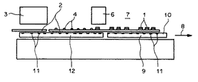
図1は、半導体チップ1を可撓性基板2上に取り付けするための装置の概略構成を示した図である。この装置は、基板2の基板サイト5(図3参照)に接着剤4を付与するための供給ステーション3と、基板サイト5に半導体チップ1を装着するための接着ステーション6と、接着剤4を固化するための硬化ステーション7(curing station)とを有し、これらは、基板2の搬送方向8に沿って順番に配置されている。硬化ステーション7は、移動可能な加熱板9を備えている。その基板2に面した側の支持面10は、基板2を吸い付けるために真空状態におくことができる溝11を有している。さらに、該取り付け装置は、上記加熱板9とともに移動可能とされた支持板12を備えている。この加熱板9もまた、基板2を吸い付けるために真空状態におくことができる溝11を有している。加熱板9と支持板12を搬送方向8、ならびに搬送方向8に直交する方向13(図2参照)に動かすための二つの駆動装置が設けられている。
【0015】
図2は、支持板12及び加熱板9の平面図である。機構的には、支持板12及び加熱板9は堅固に連結されているが、ギャップ14によって隔てられている。これにより、加熱板9から支持板12へ大量の熱が伝わらないようにされており、このため、接着剤9が固化し始めるのは、基板サイト5が加熱板9上に位置してからになるようになっている。溝11は、ドリルホール15を介して真空生成源に接続されている。個々の溝11の位置と長さ寸法は、基板2が支持板12や加熱板9上で完全に平らに維持されるようにその全領域にわたって吸い付けられるよう、設定されている。加熱板9は、溝11を備える二つの領域を有し、これにより、接着剤4が2サイクルに亘って硬化されるようになっている。
【0016】
図3は、基板2の平面図である。複数の基板サイト5は、m個の行17とn個の列18からなるブロック16の中に配列されている。例には、m=3、かつ、n=4の場合が示されている。列18から列18までの間の距離は、符号Cで記され、ブロック16からブロック16までは、符号Bで記されている。
【0017】
上記取り付け装置の操作において、基板サイト5は複数のブロックにおいて処理される。すなわち、供給ステーション3で、一番目のブロック16の基板サイト5に接着剤4が付与される。接着ステーション6で、二番目のブロック16の基板サイト5上に半導体チップ1が配置される。硬化ステーション7においては、三番目と四番目のブロック16の基板サイト5に対して接着剤4が固化される。その時々に応じて、四つのブロック16は、同一の基板2に属するか、あるいは、異なる複数の基板2に属することになる。複数のブロックによる処理は、次のことを意味している。すなわち、ブロック16のm×n個の基板サイト5を処理している間、基板2が継続的に支持板12及び加熱板9に固定されたままであるということである。m×n個の基板サイト5を備えたブロック16が完全に半導体チップ1によって装着されたときのみ、真空状態が解除され、基板2が搬送方向8に、B−(n−1)×Cの距離だけ送られる。同時に、支持板12及び加熱板9は、搬送方向8と反対の方向に、予め定められたスタート位置まで(n−1)×Cの距離だけ戻される。その後、基板2が平らな状態に維持され、支持板12上、そしてまた加熱板9上に固定されるように、支持板12ならびに加熱板9の溝11が真空状態におかれる。続いて、供給ステーション3で、次のブロック16の基板サイト5に接着剤4が付与されるとともに、接着ステーション6では、先に接着剤4が付与された基板サイト5に、半導体チップ1が列18毎に装着される。一つの列18が完全に装着されると、次の列18の装着を行うため、支持板12及び加熱板9は、真空状態を維持したまま搬送方向8に、Cの距離だけ一緒に送られる。こうすることにより、基板2は、支持板12及び加熱板9の上に固定されたまま、これらともども移動させられる。一つのブロック16の最後の列18が装着されると、真空状態の解除と、基板2の距離B−(n−1)×Cの送りと、支持板12及び加熱板9の距離(n−1)×Cの戻りとによって、上述した如く、次のサイクルが開始される。
【0018】
接着ステーション6が半導体チップ1を予め定められた位置に常に配置する場合でも、支持板12及び加熱板9は、列18の中に位置しているm個の基板サイト5に装着を行うために、方向13、すなわち、搬送方向8に直角な方向にも移動させられる。
【0019】
図4は、接着剤4を硬化させるためのオーブン19の断面を示す図である。オーブン19は、移動自在なマガジン20を有している。このマガジン20は、基板2を吸い付けるために真空状態におくことができる溝11を有するプレート21を多数備えている。オーブン19の外で、やや冷めた条件のもとで、マガジン20に基板2が搭載され、固化の開始前に基板2がプレート21上に平らに維持されるよう、プレート21の溝11が真空状態におかれる。
【0020】
図5は、連続オーブンとして形成された、さらに他のオーブン19の断面を示す図である。半導体チップ1が装着された基板2は、次々にオーブン19を通ってフィードスルー方向に搬送される。基板2は、プレート21上に保持されたままとなる。ここで、プレート21は、基板2がプレート21上に平らに維持されるように、基板2を吸い付けるために真空状態におくことのできる溝11を有している。
【図面の簡単な説明】
【図1】半導体チップを取り付けるための装置を示す図である。
【図2】支持板及び加熱板を示す図である。
【図3】基板を示す図である。
【図4】オーブンを示す図である。
【図5】他の実施形態によるオーブンを示す図である。
【符号の説明】
1・・・半導体チップ
2・・・基板
3・・・供給ステーション
4・・・接着剤
5・・・基板サイト
6・・・接着ステーション
7・・・硬化ステーション
8・・・搬送方向
9・・・加熱板
10・・・支持面
11・・・溝
12・・・支持板
16・・・ブロック
19・・・オーブン[0001]
BACKGROUND OF THE INVENTION
The present invention relates to a method and apparatus for mounting a semiconductor on a flexible substrate.
[0002]
[Prior art]
In the semiconductor industry, apart from metal substrates that have already proven useful, flexible substrates such as BGA® flextape are increasingly being used. Furthermore, such flex tapes are becoming thinner and have reached a thickness of only 50 μm. As a result, the uneven thickness of the adhesive between the semiconductor chip and the flex tape poses various difficulties related to the mounting of the semiconductor chip, such as the tilt and inaccurate position of the semiconductor chip. In addition, the quality of the bond due to the adhesive can be severely compromised, such as the adhesive flowing around in various phases, constricting, and locally dissociating before final solidification. . Bond pad contamination can also be attributed to this.
[0003]
[Problems to be solved by the invention]
The present invention has been made in view of the above circumstances, and it is an object of the present invention to provide a method and an apparatus capable of mounting a semiconductor chip on a flexible substrate with high reliability and quality.
[0004]
[Means for Solving the Problems]
The features of the present invention are described in
[0005]
This problem is solved by the present invention that the substrate is supported flat on the level support surface at least during the adhesive setting, but more preferably during all critical phases of the attachment process. .
[0006]
As a first solution, an automatic assembly apparatus, which is a so-called die bonder, is provided with a heating plate for immediately hardening an adhesive after mounting a semiconductor chip. The heating plate has grooves or elongated depressions on the support surface facing the substrate that are placed in a vacuum to support the substrate flat until the adhesive is solidified. In addition, more preferably, the automatic assembling apparatus is provided with a support plate, which also supports the substrate on the level support surface while applying the adhesive or placing the semiconductor chip. It has a groove or elongated depression that is placed in a vacuum to suck the entire area.
[0007]
This solution is particularly suitable for the processing of so-called matrix substrates. Using this matrix substrate, a plurality of substrate sites for a plurality of semiconductor chips are arranged adjacent to each other in a plurality of blocks consisting of n rows and m columns on the substrate. The The attachment of the semiconductor chip is performed in three steps as usual. That is, in the first step, adhesive is applied to the substrate site at a dispensing station. In the second step, semiconductor chips are placed on the substrate site at a bonding station. In the third step, the adhesive is hardened. In order to obtain sufficient time for the adhesive to solidify, such a matrix substrate is processed in a plurality of blocks as follows. That is, as soon as one block having n × m substrate sites is completely mounted by the semiconductor chip, the vacuum state is released and the substrate is sent in the transport direction. At the same time, the support plate and the heating plate are returned to a predetermined start position in the direction opposite to the transport direction. Thereafter, the grooves of the support plate and the heating plate are placed in a vacuum state so that the substrate is placed and fixed flat on the support plate and the heating plate. Subsequently, an adhesive is applied to the next n × m substrate sites at the supply station, and at the bonding station, semiconductor chips are provided for each column at the substrate site to which the adhesive has been previously applied. . When one row is completely mounted, the support plate and the heating plate are sent together in the transport direction while maintaining a vacuum state in order to mount the next row. The substrate is thus moved back together while being fixed on the support plate and the heating plate. When the last row of one block is installed, the next cycle is started as described above by releasing the vacuum, feeding the substrate, and returning the support plate and the heating plate.
[0008]
Curing time can be doubled or tripled by forming the heating plate with two to three heating positions. In order to be able to keep the throughput rate of the automated assembly equipment relatively high, the solution must be placed relatively fast.
[0009]
For some applications, it is sufficient for the adhesive to be only partially cured, for example 80%. The remainder is solidified in subsequent processing steps, such as during wiring on the wire bonding apparatus.
[0010]
In the second solution, the adhesive is not solidified on the automatic assembly device, but solidified in the oven. As time passes in the oven, it is guaranteed that the substrate rests flat on the support means. A plate having a groove or an elongated depression placed in a vacuum state so that the substrate can be sucked is provided as a support means. Although not necessary, the plate itself can be heated. This solution also allows the adhesive to be placed slowly.
[0011]
As a result, the quality of the attachment is greatly improved by the present invention. Since the substrate is kept flat while the adhesive is solidified, an adhesive layer having a uniform thickness is formed between the substrate and the semiconductor chip. That is, the semiconductor chip can no longer be bent by the adhesive during solidification. Furthermore, better uniformity of the adhesive is achieved. This means that when the adhesive is hardened in the usual way, the different components of the adhesive, for example, segregate into several areas containing a large amount of silver as well as some areas containing only a small amount of silver. This is in contrast to what could be possible or even empty.
[0012]
Furthermore, since the substrate is placed flat on the heating plate, reliable heat transfer from the heating plate to the adhesive is ensured. This is very important when the heat transfer properties have a decisive influence on the curing time required to fully solidify the adhesive.
[0013]
DETAILED DESCRIPTION OF THE INVENTION
Hereinafter, embodiments of the present invention will be described in detail with reference to the drawings.
[0014]
FIG. 1 is a diagram showing a schematic configuration of an apparatus for mounting a
[0015]
FIG. 2 is a plan view of the
[0016]
FIG. 3 is a plan view of the
[0017]
In operation of the mounting apparatus, the substrate site 5 is processed in a plurality of blocks. That is, the adhesive 4 is applied to the substrate site 5 of the
[0018]
Even when the
[0019]
FIG. 4 is a view showing a cross section of an
[0020]
FIG. 5 shows a cross section of yet another
[Brief description of the drawings]
FIG. 1 is a diagram showing an apparatus for attaching a semiconductor chip.
FIG. 2 is a view showing a support plate and a heating plate.
FIG. 3 is a diagram showing a substrate.
FIG. 4 is a diagram showing an oven.
FIG. 5 shows an oven according to another embodiment.
[Explanation of symbols]
DESCRIPTION OF
Claims (2)
供給ステーション(3)にて前記可撓性基板(2)上の前記基板サイト(5)に接着剤(4)を付与し、前記可撓性基板(2)の搬送方向において前記供給ステーション(3)の後に配置された接着ステーション(6)にて前記基板サイト(5)上に複数の前記半導体チップ(1)を載置し、前記可撓性基板(2)の搬送方向において前記接着ステーション(6)の後に配置された硬化ステーション(7)にて前記接着剤(4)を硬化する方法において、
前記接着剤(4)を硬化させる間、前記可撓性基板(2)は加熱板(9)の平らな支持面(10)上に、真空によって固定され、
前記加熱板(9)は、前記接着剤(4)を付与する間、及び前記半導体チップ(1)を配置する間、前記可撓性基板(2)を平らに固定するように真空を付与することができる流路又は溝を有する支持板(12)に堅固に連結されており、
前記基板サイト(5)は、ブロックごとに、
前記可撓性基板(2)を搬送方向に搬送するステップ、
前記支持板(12)及び前記加熱板(9)を真空引きするステップ、
前記支持板(12)及び前記加熱板(9)を複数の予め定められた位置に繰り返して移動させ、前記位置それぞれにて前記接着剤が前記接着ステーション(3)における前記基板サイト(5)に付与され、前記半導体チップ(1)が前記接着ステーション(6)における他の基板サイト(5)上に配置されるステップ、
前記真空引きを停止するステップ、及び
前記可撓性基板(2)を前記搬送方向に搬送し、同時に前記支持板(12)及び前記加熱板(9)を前記搬送方向とは反対の方向に移動するステップ、
によって処理されることを特徴とする方法。 A method of mounting a semiconductor chip (1) on a flexible substrate (2) having a plurality of substrate sites (5) arranged in a plurality of blocks (16),
Adhesive (4) is applied to the substrate site (5 ) on the flexible substrate (2) at the supply station (3), and the supply station (3) in the transport direction of the flexible substrate (2). ) placing a plurality of said semiconductor chip (1) to the substrate site (5) on at arranged bonding station (6) after said flexible the bonding station in the conveying direction of the substrate (2) ( a method of curing the adhesive (4) in arranged curing station after 6) (7),
During curing the adhesive (4), the flexible substrate (2) is on the flat support surface of the heating plate (9) (10), is fixed by the vacuum,
The heating plate (9) applies a vacuum so as to fix the flexible substrate (2) flatly while applying the adhesive (4) and placing the semiconductor chip (1). Rigidly connected to a support plate (12) having a flow path or groove capable of
The substrate site (5) is
Transporting the flexible substrate (2) in a transport direction;
Evacuating the support plate (12) and the heating plate (9);
The support plate (12) and the heating plate (9) are repeatedly moved to a plurality of predetermined positions, and the adhesive is transferred to the substrate site (5) in the bonding station (3) at each of the positions. Applied and the semiconductor chip (1) is placed on another substrate site (5) in the bonding station (6);
Stopping the evacuation; and
Transporting the flexible substrate (2) in the transport direction and simultaneously moving the support plate (12) and the heating plate (9) in a direction opposite to the transport direction;
A method characterized by being processed by :
前記可撓性基板(2)に半導体チップ(1)を装着する接着ステーション(6)であって、前記可撓性基板の搬送方向において前記供給ステーションの後に配置された前記接着ステーション(6)と、
前記可撓性基板(2)のための支持板(12)であって、前記接着剤(4)を付与する間、及び前記半導体チップ(1)を載置する間、前記可撓性基板(2)を平らに固定するために真空が付与される溝(11)を有する支持板(12)と、
前記接着剤を硬化させるための加熱板(9)であって、前記可撓性基板の搬送方向において前記支持板(12)の後に配置されているとともに前記可撓性基板(2)を吸い付けるために真空が付与される溝(11)を有する加熱板(9)と、
を備える、前記可撓性基板(2)上に半導体チップ(1)を取り付ける装置であって、
前記支持板(12)と前記加熱板(9)とは、互いに堅固に連結されているとともに、前記搬送方向に移動可能であることを特徴とする装置。A supply station (3) for applying an adhesive (4) to the flexible substrate (2) ;
An adhering station (6) for mounting the semiconductor chip (1) on the flexible substrate (2), the adhering station (6) arranged after the supplying station in the conveying direction of the flexible substrate ; ,
A support plate for the flexible substrate (2) (12), while placing between, and the semiconductor chip (1) for applying the adhesive (4), the flexible substrate ( A support plate (12) having a groove (11) to which a vacuum is applied to fix 2) flatly;
A heating plate (9) for curing the adhesive, which is disposed behind the support plate (12) in the transport direction of the flexible substrate and sucks the flexible substrate (2) A heating plate (9) having a groove (11) to which a vacuum is applied for,
An apparatus for mounting a semiconductor chip (1) on the flexible substrate (2), comprising:
The support plate (12) and the heating plate (9) are firmly connected to each other and movable in the transport direction .
Applications Claiming Priority (2)
| Application Number | Priority Date | Filing Date | Title |
|---|---|---|---|
| EP00810577.7 | 2000-07-03 | ||
| EP20000810577 EP1170787A1 (en) | 2000-07-03 | 2000-07-03 | Method and apparatus for mounting semiconductor chips on a flexible substrate |
Publications (3)
| Publication Number | Publication Date |
|---|---|
| JP2002050643A JP2002050643A (en) | 2002-02-15 |
| JP2002050643A5 JP2002050643A5 (en) | 2008-08-14 |
| JP5079192B2 true JP5079192B2 (en) | 2012-11-21 |
Family
ID=8174785
Family Applications (1)
| Application Number | Title | Priority Date | Filing Date |
|---|---|---|---|
| JP2001197085A Expired - Fee Related JP5079192B2 (en) | 2000-07-03 | 2001-06-28 | Method and apparatus for mounting semiconductor chip on flexible substrate |
Country Status (2)
| Country | Link |
|---|---|
| EP (1) | EP1170787A1 (en) |
| JP (1) | JP5079192B2 (en) |
Families Citing this family (3)
| Publication number | Priority date | Publication date | Assignee | Title |
|---|---|---|---|---|
| DE10245398B3 (en) * | 2002-09-28 | 2004-06-03 | Mühlbauer Ag | Device and method for applying semiconductor chips to carriers |
| KR100673543B1 (en) * | 2006-02-15 | 2007-01-25 | 노드슨상산 주식회사 | Apparatus for curing membrane of proton exchange type fuel cell |
| US8444328B2 (en) | 2009-12-11 | 2013-05-21 | International Business Machines Corporation | Electro-optical assembly fabrication |
Family Cites Families (7)
| Publication number | Priority date | Publication date | Assignee | Title |
|---|---|---|---|---|
| JPS63114220A (en) * | 1986-10-31 | 1988-05-19 | Matsushita Electric Ind Co Ltd | Chip bonding device |
| JPS6384939U (en) * | 1986-11-21 | 1988-06-03 | ||
| JPS63190400A (en) * | 1987-02-03 | 1988-08-05 | 株式会社東芝 | Flexible printed circuit aligner |
| JPH0250441A (en) * | 1988-08-12 | 1990-02-20 | Nec Kyushu Ltd | Semiconductor manufacturing apparatus |
| US5173766A (en) * | 1990-06-25 | 1992-12-22 | Lsi Logic Corporation | Semiconductor device package and method of making such a package |
| US5548091A (en) * | 1993-10-26 | 1996-08-20 | Tessera, Inc. | Semiconductor chip connection components with adhesives and methods for bonding to the chip |
| JPH11121499A (en) * | 1997-10-13 | 1999-04-30 | Matsushita Electron Corp | Method and device for manufacture of semiconductor device |
-
2000
- 2000-07-03 EP EP20000810577 patent/EP1170787A1/en not_active Withdrawn
-
2001
- 2001-06-28 JP JP2001197085A patent/JP5079192B2/en not_active Expired - Fee Related
Also Published As
| Publication number | Publication date |
|---|---|
| EP1170787A1 (en) | 2002-01-09 |
| JP2002050643A (en) | 2002-02-15 |
Similar Documents
| Publication | Publication Date | Title |
|---|---|---|
| JPH11512875A (en) | Connecting multiple microelectronic devices with lead deformation. | |
| JP2830852B2 (en) | Electronic component mounting method | |
| US6982211B2 (en) | Water jet processing method | |
| US20050011934A1 (en) | Apparatus and method for bonding electronic component, circuit board, and electronic component mounting apparatus | |
| KR20160108196A (en) | Method for manufacturing semiconductor device | |
| US20030094241A1 (en) | Die bonder | |
| TWI527147B (en) | Method and apparatus for mounting semiconductor chips | |
| JP5079192B2 (en) | Method and apparatus for mounting semiconductor chip on flexible substrate | |
| JPH11163006A (en) | Method for bonding pellet | |
| KR101994667B1 (en) | Electronic component mounting device and method for producing electronic component | |
| KR100746386B1 (en) | Method and apparatus for mounting semiconductor chips onto a flexible substrate | |
| JP2001135765A (en) | Method and device for manufacturing composite lead frame | |
| US7028397B2 (en) | Method of attaching a semiconductor chip to a chip mounting substrate | |
| EP1170788A2 (en) | Method and apparatus for mounting semiconductor chips onto a flexible substrate | |
| US7498202B2 (en) | Method for die attaching | |
| JP2013016771A (en) | Nondefective board array module and method of manufacturing the same | |
| JP2005123609A (en) | Die bonder equipment and method for adhering semiconductor chip using same | |
| JP2003078069A (en) | Pseudo wafer for multichip module production and production method therefor | |
| JPH11251335A (en) | Mounting device for semiconductor element and mounting method therefor | |
| JPH04122093A (en) | Paste transfer method and transfer jig | |
| JP2005056901A (en) | Apparatus and process for manufacturing semiconductor device | |
| JP3394667B2 (en) | Semiconductor manufacturing equipment | |
| JPH10135278A (en) | Method of mounting electronic component onto carrier tape and its equipment | |
| JP2733179B2 (en) | Hybrid integrated circuit manufacturing equipment | |
| JP2023134301A (en) | Semiconductor manufacturing device, coating applicator, and manufacturing method of semiconductor device |
Legal Events
| Date | Code | Title | Description |
|---|---|---|---|
| A521 | Written amendment |
Free format text: JAPANESE INTERMEDIATE CODE: A523 Effective date: 20080619 |
|
| A621 | Written request for application examination |
Free format text: JAPANESE INTERMEDIATE CODE: A621 Effective date: 20080619 |
|
| A521 | Written amendment |
Free format text: JAPANESE INTERMEDIATE CODE: A523 Effective date: 20080625 |
|
| A711 | Notification of change in applicant |
Free format text: JAPANESE INTERMEDIATE CODE: A712 Effective date: 20080627 |
|
| A977 | Report on retrieval |
Free format text: JAPANESE INTERMEDIATE CODE: A971007 Effective date: 20110124 |
|
| A131 | Notification of reasons for refusal |
Free format text: JAPANESE INTERMEDIATE CODE: A131 Effective date: 20110201 |
|
| A601 | Written request for extension of time |
Free format text: JAPANESE INTERMEDIATE CODE: A601 Effective date: 20110426 |
|
| A602 | Written permission of extension of time |
Free format text: JAPANESE INTERMEDIATE CODE: A602 Effective date: 20110502 |
|
| A521 | Written amendment |
Free format text: JAPANESE INTERMEDIATE CODE: A523 Effective date: 20110526 |
|
| A131 | Notification of reasons for refusal |
Free format text: JAPANESE INTERMEDIATE CODE: A131 Effective date: 20111220 |
|
| A521 | Written amendment |
Free format text: JAPANESE INTERMEDIATE CODE: A523 Effective date: 20120308 |
|
| A131 | Notification of reasons for refusal |
Free format text: JAPANESE INTERMEDIATE CODE: A131 Effective date: 20120403 |
|
| A521 | Written amendment |
Free format text: JAPANESE INTERMEDIATE CODE: A523 Effective date: 20120628 |
|
| TRDD | Decision of grant or rejection written | ||
| A01 | Written decision to grant a patent or to grant a registration (utility model) |
Free format text: JAPANESE INTERMEDIATE CODE: A01 Effective date: 20120731 |
|
| A01 | Written decision to grant a patent or to grant a registration (utility model) |
Free format text: JAPANESE INTERMEDIATE CODE: A01 |
|
| A61 | First payment of annual fees (during grant procedure) |
Free format text: JAPANESE INTERMEDIATE CODE: A61 Effective date: 20120829 |
|
| FPAY | Renewal fee payment (prs date is renewal date of database) |
Free format text: PAYMENT UNTIL: 20150907 Year of fee payment: 3 |
|
| R150 | Certificate of patent (=grant) or registration of utility model |
Free format text: JAPANESE INTERMEDIATE CODE: R150 |
|
| LAPS | Cancellation because of no payment of annual fees |