JP5077458B2 - 回路基板用端子 - Google Patents
回路基板用端子 Download PDFInfo
- Publication number
- JP5077458B2 JP5077458B2 JP2011072783A JP2011072783A JP5077458B2 JP 5077458 B2 JP5077458 B2 JP 5077458B2 JP 2011072783 A JP2011072783 A JP 2011072783A JP 2011072783 A JP2011072783 A JP 2011072783A JP 5077458 B2 JP5077458 B2 JP 5077458B2
- Authority
- JP
- Japan
- Prior art keywords
- terminal
- circuit board
- fitting portion
- plate width
- fitting
- Prior art date
- Legal status (The legal status is an assumption and is not a legal conclusion. Google has not performed a legal analysis and makes no representation as to the accuracy of the status listed.)
- Expired - Fee Related
Links
- 238000005452 bending Methods 0.000 claims description 4
- 238000005476 soldering Methods 0.000 description 17
- 238000000034 method Methods 0.000 description 7
- 230000017525 heat dissipation Effects 0.000 description 6
- 230000035882 stress Effects 0.000 description 6
- 238000004519 manufacturing process Methods 0.000 description 4
- 239000000463 material Substances 0.000 description 4
- 229910052751 metal Inorganic materials 0.000 description 4
- 239000002184 metal Substances 0.000 description 4
- 230000007423 decrease Effects 0.000 description 3
- 238000005304 joining Methods 0.000 description 3
- 230000008646 thermal stress Effects 0.000 description 3
- 238000005520 cutting process Methods 0.000 description 2
- 230000005611 electricity Effects 0.000 description 2
- 230000020169 heat generation Effects 0.000 description 2
- 238000003780 insertion Methods 0.000 description 2
- 230000037431 insertion Effects 0.000 description 2
- 229910000838 Al alloy Inorganic materials 0.000 description 1
- RYGMFSIKBFXOCR-UHFFFAOYSA-N Copper Chemical compound [Cu] RYGMFSIKBFXOCR-UHFFFAOYSA-N 0.000 description 1
- 229910000881 Cu alloy Inorganic materials 0.000 description 1
- 229910052782 aluminium Inorganic materials 0.000 description 1
- XAGFODPZIPBFFR-UHFFFAOYSA-N aluminium Chemical compound [Al] XAGFODPZIPBFFR-UHFFFAOYSA-N 0.000 description 1
- 239000004020 conductor Substances 0.000 description 1
- 229910052802 copper Inorganic materials 0.000 description 1
- 239000010949 copper Substances 0.000 description 1
- 238000005336 cracking Methods 0.000 description 1
- 238000006073 displacement reaction Methods 0.000 description 1
- 230000005489 elastic deformation Effects 0.000 description 1
- 238000009413 insulation Methods 0.000 description 1
- 229920003023 plastic Polymers 0.000 description 1
- 239000004033 plastic Substances 0.000 description 1
- 238000007747 plating Methods 0.000 description 1
- 239000002994 raw material Substances 0.000 description 1
- 238000005096 rolling process Methods 0.000 description 1
- 229910000679 solder Inorganic materials 0.000 description 1
- 229920003002 synthetic resin Polymers 0.000 description 1
- 239000000057 synthetic resin Substances 0.000 description 1
Images
Landscapes
- Coupling Device And Connection With Printed Circuit (AREA)
Description
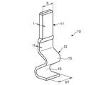
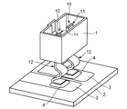
2 回路基板
3 回路パターン
4 半田付け
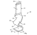
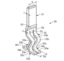
10,20,30 回路基板用端子
11,21,31 嵌合部
12,22,32 端子部
13,23,33a,33b,33c 折曲部
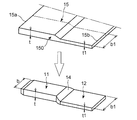
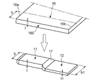
14,17,24 境界部
15,16 金属板
15a,16a 基端部
15b,16b 先端部
21c 仮想軸線
25 捻転部
26 接合部
26g 幅
32a,32b,32c 端子片
32u,32v,32w 先端部
150,160 条材
t,t1 板厚
b,b1,b2,b3 板幅
s1,s2 スリット
Claims (5)
- 電気回路用コネクタの絶縁ハウジングに固定される嵌合部と、回路基板に接合するため前記嵌合部から延設された端子部とを有する帯板状の回路基板用端子であって、前記端子部の板厚を前記嵌合部の板厚より小とし、前記端子部の板幅を前記嵌合部の板幅より大とし、前記端子部にその板厚方向に撓んだ折曲部を設けた回路基板用端子。
- 前記嵌合部の横断面の面積と、前記端子部の横断面の面積と、が略同等である請求項1記載の回路基板用端子。
- 前記嵌合部と前記端子部との間に、それぞれの板幅方向が、前記嵌合部の仮想軸線を中心に相対的に回転変位した捻転部を設けた請求項1または2記載の回路基板用端子。
- 電気回路用コネクタの絶縁ハウジングに固定される嵌合部と、回路基板に接合するため前記嵌合部から延設された端子部とを有する帯板状の回路基板用端子であって、前記端子部の板厚を前記嵌合部の板厚より小とし、前記端子部の板幅を前記嵌合部の板幅より大とし、前記端子部に、その板幅方向と交差するスリットを開設することにより複数の櫛状端子片を設け、前記端子片にその板厚方向に撓んだ折曲部を設け、少なくとも前記端子部の板幅方向の両側に位置する前記端子片の先端部を互いに接近するように変位させたことを特徴とする回路基板用端子。
- 隣り合う前記端子片の先端部が交互に反対を向く方向に撓ませた請求項4記載の回路基板用端子。
Priority Applications (1)
| Application Number | Priority Date | Filing Date | Title |
|---|---|---|---|
| JP2011072783A JP5077458B2 (ja) | 2011-03-29 | 2011-03-29 | 回路基板用端子 |
Applications Claiming Priority (1)
| Application Number | Priority Date | Filing Date | Title |
|---|---|---|---|
| JP2011072783A JP5077458B2 (ja) | 2011-03-29 | 2011-03-29 | 回路基板用端子 |
Publications (2)
| Publication Number | Publication Date |
|---|---|
| JP2012209075A JP2012209075A (ja) | 2012-10-25 |
| JP5077458B2 true JP5077458B2 (ja) | 2012-11-21 |
Family
ID=47188653
Family Applications (1)
| Application Number | Title | Priority Date | Filing Date |
|---|---|---|---|
| JP2011072783A Expired - Fee Related JP5077458B2 (ja) | 2011-03-29 | 2011-03-29 | 回路基板用端子 |
Country Status (1)
| Country | Link |
|---|---|
| JP (1) | JP5077458B2 (ja) |
Families Citing this family (5)
| Publication number | Priority date | Publication date | Assignee | Title |
|---|---|---|---|---|
| JP7454982B2 (ja) * | 2020-03-30 | 2024-03-25 | 新電元工業株式会社 | 接続端子及び電子装置 |
| JP7600504B2 (ja) * | 2020-12-28 | 2024-12-17 | ヒロセ電機株式会社 | 電気コネクタ |
| JP7711548B2 (ja) * | 2021-10-19 | 2025-07-23 | オムロン株式会社 | 電磁継電器 |
| CN116365268A (zh) * | 2021-12-28 | 2023-06-30 | 捷拓科技股份有限公司 | 端子 |
| JP7792065B2 (ja) * | 2022-06-09 | 2025-12-25 | 株式会社オートネットワーク技術研究所 | 端子金具 |
Family Cites Families (1)
| Publication number | Priority date | Publication date | Assignee | Title |
|---|---|---|---|---|
| US5167513A (en) * | 1991-08-14 | 1992-12-01 | International Business Machines Corp. | Load limited pin for an electrical connector |
-
2011
- 2011-03-29 JP JP2011072783A patent/JP5077458B2/ja not_active Expired - Fee Related
Also Published As
| Publication number | Publication date |
|---|---|
| JP2012209075A (ja) | 2012-10-25 |
Similar Documents
| Publication | Publication Date | Title |
|---|---|---|
| JP6413096B2 (ja) | コイル部品 | |
| JP5298336B2 (ja) | シャント抵抗器およびその製造方法 | |
| JP5077458B2 (ja) | 回路基板用端子 | |
| JP6167294B2 (ja) | コイル部品 | |
| CN102842794A (zh) | 接触件及插座 | |
| JP5939706B2 (ja) | バスバ | |
| JP2005353567A (ja) | プレスフィット端子およびそれを用いた回路基板モジュール | |
| JP2011077022A (ja) | 基板用端子 | |
| JP6124953B2 (ja) | 二厚ダブルエンド雄型ブレード端子及びその製造方法 | |
| JP6827019B2 (ja) | プレスフィット端子及び基板組立体 | |
| JP4844512B2 (ja) | 回路基板と配線導体とを電気的に接続する端子の固定構造及び回路基板と配線導体とを電気的に接続する端子の固定方法 | |
| WO2016167095A1 (ja) | プレスフィット端子及び基板用コネクタ | |
| JP7567261B2 (ja) | 電流検出装置 | |
| JP5622051B2 (ja) | 基板用端子およびそれを用いた基板用コネクタ | |
| JP6307365B2 (ja) | 端子、端子取付構造及び前記端子を備える電気接続箱 | |
| JP5816065B2 (ja) | 接続体 | |
| JP2013125581A (ja) | 電気コネクタ | |
| JP2010123618A (ja) | 端子付部品を備えたプリント基板 | |
| JP5151936B2 (ja) | 端子金具及びその製造方法 | |
| CN100479263C (zh) | 接地端子及设有该接地端子的电子设备 | |
| CN203326170U (zh) | 导电端子 | |
| JP6440468B2 (ja) | 圧着端子 | |
| JP7486037B2 (ja) | フレキシブルプリント基板の接続構造およびフレキシブルプリント基板ユニットの製造方法 | |
| JP2011253991A (ja) | プリント基板積層体 | |
| JP2019517711A (ja) | 大きく曲がったはんだ付けピンを有する電気接続アセンブリ |
Legal Events
| Date | Code | Title | Description |
|---|---|---|---|
| TRDD | Decision of grant or rejection written | ||
| A01 | Written decision to grant a patent or to grant a registration (utility model) |
Free format text: JAPANESE INTERMEDIATE CODE: A01 Effective date: 20120731 |
|
| A01 | Written decision to grant a patent or to grant a registration (utility model) |
Free format text: JAPANESE INTERMEDIATE CODE: A01 |
|
| A61 | First payment of annual fees (during grant procedure) |
Free format text: JAPANESE INTERMEDIATE CODE: A61 Effective date: 20120813 |
|
| FPAY | Renewal fee payment (event date is renewal date of database) |
Free format text: PAYMENT UNTIL: 20150907 Year of fee payment: 3 |
|
| R150 | Certificate of patent or registration of utility model |
Ref document number: 5077458 Country of ref document: JP Free format text: JAPANESE INTERMEDIATE CODE: R150 Free format text: JAPANESE INTERMEDIATE CODE: R150 |
|
| R250 | Receipt of annual fees |
Free format text: JAPANESE INTERMEDIATE CODE: R250 |
|
| R250 | Receipt of annual fees |
Free format text: JAPANESE INTERMEDIATE CODE: R250 |
|
| R250 | Receipt of annual fees |
Free format text: JAPANESE INTERMEDIATE CODE: R250 |
|
| R250 | Receipt of annual fees |
Free format text: JAPANESE INTERMEDIATE CODE: R250 |
|
| R250 | Receipt of annual fees |
Free format text: JAPANESE INTERMEDIATE CODE: R250 |
|
| R250 | Receipt of annual fees |
Free format text: JAPANESE INTERMEDIATE CODE: R250 |
|
| LAPS | Cancellation because of no payment of annual fees |