JP5077458B2 - Circuit board terminal - Google Patents
Circuit board terminal Download PDFInfo
- Publication number
- JP5077458B2 JP5077458B2 JP2011072783A JP2011072783A JP5077458B2 JP 5077458 B2 JP5077458 B2 JP 5077458B2 JP 2011072783 A JP2011072783 A JP 2011072783A JP 2011072783 A JP2011072783 A JP 2011072783A JP 5077458 B2 JP5077458 B2 JP 5077458B2
- Authority
- JP
- Japan
- Prior art keywords
- terminal
- circuit board
- fitting portion
- plate width
- fitting
- Prior art date
- Legal status (The legal status is an assumption and is not a legal conclusion. Google has not performed a legal analysis and makes no representation as to the accuracy of the status listed.)
- Expired - Fee Related
Links
- 238000005452 bending Methods 0.000 claims description 4
- 238000005476 soldering Methods 0.000 description 17
- 238000000034 method Methods 0.000 description 7
- 230000017525 heat dissipation Effects 0.000 description 6
- 230000035882 stress Effects 0.000 description 6
- 238000004519 manufacturing process Methods 0.000 description 4
- 239000000463 material Substances 0.000 description 4
- 229910052751 metal Inorganic materials 0.000 description 4
- 239000002184 metal Substances 0.000 description 4
- 230000007423 decrease Effects 0.000 description 3
- 238000005304 joining Methods 0.000 description 3
- 230000008646 thermal stress Effects 0.000 description 3
- 238000005520 cutting process Methods 0.000 description 2
- 230000005611 electricity Effects 0.000 description 2
- 230000020169 heat generation Effects 0.000 description 2
- 238000003780 insertion Methods 0.000 description 2
- 230000037431 insertion Effects 0.000 description 2
- 229910000838 Al alloy Inorganic materials 0.000 description 1
- RYGMFSIKBFXOCR-UHFFFAOYSA-N Copper Chemical compound [Cu] RYGMFSIKBFXOCR-UHFFFAOYSA-N 0.000 description 1
- 229910000881 Cu alloy Inorganic materials 0.000 description 1
- 229910052782 aluminium Inorganic materials 0.000 description 1
- XAGFODPZIPBFFR-UHFFFAOYSA-N aluminium Chemical compound [Al] XAGFODPZIPBFFR-UHFFFAOYSA-N 0.000 description 1
- 239000004020 conductor Substances 0.000 description 1
- 229910052802 copper Inorganic materials 0.000 description 1
- 239000010949 copper Substances 0.000 description 1
- 238000005336 cracking Methods 0.000 description 1
- 238000006073 displacement reaction Methods 0.000 description 1
- 230000005489 elastic deformation Effects 0.000 description 1
- 238000009413 insulation Methods 0.000 description 1
- 229920003023 plastic Polymers 0.000 description 1
- 239000004033 plastic Substances 0.000 description 1
- 238000007747 plating Methods 0.000 description 1
- 239000002994 raw material Substances 0.000 description 1
- 238000005096 rolling process Methods 0.000 description 1
- 229910000679 solder Inorganic materials 0.000 description 1
- 229920003002 synthetic resin Polymers 0.000 description 1
- 239000000057 synthetic resin Substances 0.000 description 1
Images
Landscapes
- Coupling Device And Connection With Printed Circuit (AREA)
Description
本発明は、プリント基板などの各種回路基板との間の通電部材として、絶縁ハウジングに固定された状態で回路基板に接合される回路基板用端子に関する。 The present invention relates to a circuit board terminal that is joined to a circuit board in a state of being fixed to an insulating housing as a current-carrying member between various circuit boards such as a printed board.
プリント基板などの各種回路基板に対し、絶縁ハウジングに固定された状態で半田付けなどによって接合される回路基板用端子については、従来、様々な技術が開発されているが、本発明に関連するものとして、例えば、特許文献1記載の「プリント基板用雌端子の構造」及び特許文献2記載の「基板用コネクタ及びその端子金具」がある。
Various techniques have been developed for circuit board terminals that are bonded to various circuit boards such as printed circuit boards by soldering in a state of being fixed to an insulating housing, but are related to the present invention. For example, there are “a structure of a female terminal for printed circuit board” described in
特許文献1に記載されているプリント基板用雌端子は、バスバーなどを圧接する圧接部と、プリント基板に半田付けされる固定部とを有する平板状の雌端子であり、熱ストレスによって固定部の半田付けにクラックが入るのを防止するため、固定部の板厚が、応力を緩和できる薄い厚みに形成されている。
The female terminal for a printed circuit board described in
特許文献2に記載されている端子金具は、回路基板の複数のスルーホールに挿入するために櫛状に分岐させた複数の差込部を有するものであり、差込部を折り曲げて2枚重ね構造としてその断面積を増加させることにより、電気抵抗を抑え、通電時の発熱量を抑えている。
The terminal fitting described in
特許文献1記載のプリント基板用雌端子は、半田付けのクラック発生を防止することができる点においては優れているのであるが、固定部の板厚が薄いので、電気抵抗が高く、通電時の発熱量が大である。このため、パワー回路のように大電流が流れる回路基板において使用することが困難である。
The female terminal for printed circuit board described in
一方、特許文献2記載の端子金具は、差込部の断面積が大きいので、電気抵抗を抑え、通電時の発熱量を抑えることができるが、熱変形に伴って発生する応力を緩和する機能に欠けているので、熱ストレスによって固定部の半田付けにクラックが入ることがある。
On the other hand, since the terminal fitting described in
このように、従来の回路基板用端子においては、通電時の発熱量を抑制する構造にすると、熱ストレスによる半田付けクラックの防止が困難となり、熱ストレスによる半田付けのクラック発生を抑制する構造にすると、通電時の発熱量を抑制することが困難となるという問題が存在する。 As described above, in the conventional circuit board terminal, it is difficult to prevent soldering cracks due to thermal stress if the structure that suppresses the amount of heat generated during energization is suppressed, and the structure that suppresses the occurrence of soldering cracks due to thermal stress. Then, there exists a problem that it becomes difficult to suppress the calorific value at the time of energization.
本発明が解決しようとする課題は、回路基板用端子において、通電時の抵抗発熱量を抑制するとともに、放熱性を高め、半田付けのクラック発生を防止することにある。 The problem to be solved by the present invention is to suppress the amount of resistance heat generated at the time of energization in a circuit board terminal, to improve heat dissipation, and to prevent the occurrence of soldering cracks.
本発明の回路基板用端子は、電気回路用コネクタの絶縁ハウジングに固定される嵌合部と、回路基板に接合するため前記嵌合部から延設された端子部とを有する帯板状の回路基板用端子であって、前記端子部の板厚を前記嵌合部の板厚より小とし、前記端子部の板幅を前記嵌合部の板幅より大とし、前記端子部にその板厚方向に撓んだ折曲部を設けたことを特徴とする。 The circuit board terminal of the present invention is a belt-like circuit having a fitting portion fixed to the insulating housing of the electrical circuit connector and a terminal portion extending from the fitting portion for joining to the circuit board. A terminal for a board, wherein the plate thickness of the terminal portion is smaller than the plate thickness of the fitting portion, the plate width of the terminal portion is larger than the plate width of the fitting portion, and the plate portion has a plate thickness. A bent portion bent in the direction is provided.
このような構成とすれば、端子部の板厚を嵌合部の板厚より小さくすることによって生じる可能性のある横断面の面積の減少を、端子部の板幅を嵌合部の板幅より大きくすることによって回避することができるので、通電時の発熱量を抑制することができ、端子部に設けられた折曲部により、熱変形に伴って発生する応力を緩和することができるので、半田付けのクラック発生を防止することができる。また、端子部の板幅を増大させることによって、端子部の表面積が広がり端子部の放熱性が高まり、半田付けのクラック発生を防止する上で有効である。 With such a configuration, the reduction in the cross-sectional area that may be caused by making the thickness of the terminal portion smaller than the thickness of the fitting portion, the plate width of the terminal portion is changed to the plate width of the fitting portion. Since it can be avoided by making it larger, the amount of heat generated during energization can be suppressed, and the bending part provided in the terminal part can relieve the stress generated due to thermal deformation. The occurrence of soldering cracks can be prevented. Further, by increasing the plate width of the terminal portion, the surface area of the terminal portion is increased and the heat dissipation of the terminal portion is increased, which is effective in preventing the occurrence of soldering cracks.
また、前記嵌合部の横断面の面積と、前記端子部の横断面の面積と、を略同等とすることもできる。 Moreover, the area of the cross section of the said fitting part and the area of the cross section of the said terminal part can also be made substantially equivalent.
このような構成とすれば、嵌合部と端子部の通電断面積が略同等となるので、通電時の発熱量抑制に有効である。 With such a configuration, the energization cross-sectional areas of the fitting portion and the terminal portion are substantially equal, which is effective in suppressing the amount of heat generated during energization.
一方、前記嵌合部と前記端子部との間に、それぞれの板幅方向が、前記嵌合部の仮想軸線を中心に相対的に回転変位した捻転部を設けることもできる。 On the other hand, between the fitting part and the terminal part, a torsion part in which the respective plate width directions are rotationally displaced relatively around the virtual axis of the fitting part may be provided.
このような構成とすれば、本発明に係る複数の回路基板用端子を並列配置して使用する場合、嵌合部の板幅より端子部の板幅を大きくしたことによって生じる、端子配置間隔の増大を回避することができる。 With such a configuration, when a plurality of circuit board terminals according to the present invention are arranged in parallel, the terminal arrangement interval generated by increasing the plate width of the terminal portion from the plate width of the fitting portion is obtained. An increase can be avoided.
また、本発明の回路基板用端子は、電気回路用コネクタの絶縁ハウジングに固定される嵌合部と、回路基板に接合するため前記嵌合部から延設された端子部とを有する帯板状の回路基板用端子であって、前記端子部の板厚を前記嵌合部の板厚より小とし、前記端子部の嵌合部側の板幅を前記嵌合部の板幅より大とし、前記端子部に、その板幅方向と交差するスリットを開設することにより複数の櫛状の端子片を設け、前記端子片にその板厚方向に撓んだ折曲部を設け、少なくとも前記端子部の板幅方向の両側に位置する前記端子片の先端部を互いに接近するように変位させたことを特徴とする。 In addition, the circuit board terminal of the present invention has a strip-like shape having a fitting portion fixed to the insulating housing of the electrical circuit connector and a terminal portion extending from the fitting portion for joining to the circuit board. A terminal for a circuit board, wherein the plate thickness of the terminal portion is smaller than the plate thickness of the fitting portion, the plate width on the fitting portion side of the terminal portion is larger than the plate width of the fitting portion, The terminal portion is provided with a plurality of comb-like terminal pieces by opening slits intersecting with the plate width direction, the terminal piece is provided with a bent portion bent in the plate thickness direction, and at least the terminal portion The tip portions of the terminal pieces located on both sides in the plate width direction are displaced so as to approach each other.
このような構成とすれば、端子部の板厚を嵌合部の板厚より小さくすることによって生じる可能性のある横断面の面積の減少を、端子部の嵌合部側の板幅を嵌合部の板幅より大きくすることによって回避して通電時の発熱量を抑制し、端子部に設けられた折曲部により、熱変形に伴って発生する応力を緩和することができるので、半田付けのクラック発生を防止することができる。また、端子部に複数の櫛状の端子片を設けことにより、端子部の表面積が広がり端子部の放熱性が高まるため、半田付けのクラック発生を防止する上で有効である。 With such a configuration, the reduction in the cross-sectional area that may be caused by making the thickness of the terminal portion smaller than the thickness of the fitting portion, the plate width on the fitting portion side of the terminal portion is fitted. By avoiding by making it larger than the plate width of the joint portion, the amount of heat generated during energization can be suppressed, and the bending portion provided in the terminal portion can relieve the stress generated due to thermal deformation, so that the solder It is possible to prevent the occurrence of cracks. Further, by providing a plurality of comb-shaped terminal pieces in the terminal portion, the surface area of the terminal portion is increased and the heat dissipation of the terminal portion is increased, which is effective in preventing the occurrence of soldering cracks.
また、前記端子部の板幅方向の両側に位置する前記端子片の先端部を互いに接近するように変位させたことにより、両側に位置する端子片の先端部同士の間隔を端子部の板幅より小さくすることが可能となるため、本発明に係る複数の回路基板用端子を並列配置して使用する場合、嵌合部の板幅より端子部の板幅を大きくしたことによって生じる、端子配置間隔の増大を回避することができる。 Further, the terminal portions located on both sides in the plate width direction of the terminal portion are displaced so as to approach each other, whereby the interval between the tip portions of the terminal pieces located on both sides is changed to the plate width of the terminal portion. Since it becomes possible to make it smaller, when a plurality of circuit board terminals according to the present invention are used in parallel arrangement, the terminal arrangement is caused by making the board width of the terminal part larger than the board width of the fitting part. An increase in the interval can be avoided.
この場合、隣り合う前記端子片の先端部が交互に反対を向く方向に撓ませることが望ましい。 In this case, it is desirable to bend in the direction where the front-end | tip part of the said adjacent terminal piece turns to the opposite alternately.
このような構成とすれば、隣り合う端子片の先端部同士が重なり合うことを回避しながら、隣り合う端子片の先端部同士の間隔を狭めることが可能となるので、両側に位置する端子片の先端部同士の並列部分で形成される板幅を端子部の嵌合部側の板幅より小さくする上で有効である。 With such a configuration, it is possible to reduce the interval between the tip portions of the adjacent terminal pieces while avoiding the tip portions of the adjacent terminal pieces from overlapping each other. This is effective in making the plate width formed by the parallel portions of the tip portions smaller than the plate width on the fitting portion side of the terminal portion.
本発明により、回路基板用端子において、通電時の抵抗発熱量を抑制するとともに、放熱性を高め、半田付けのクラック発生を防止することができる。 According to the present invention, in a circuit board terminal, it is possible to suppress a resistance heat generation amount when energized, to improve heat dissipation, and to prevent occurrence of soldering cracks.
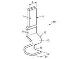
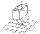
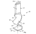
図1〜図4に基づいて、本発明の第1実施形態である回路基板用端子10について説明する。図1,図2に示すように、回路基板用端子10は、電気回路用コネクタの絶縁ハウジング1に固定される嵌合部11と、回路基板2に接合するため嵌合部11から延設された端子部12とを有する帯板状の導電性部材である。端子部12の板厚t1を嵌合部11の板厚tより小とし、端子部12の板幅b1を嵌合部11の板幅bより大とするとともに、端子部12にその板厚t1方向に撓んだ複数の折曲部13を設けている。
The
回路基板用端子10の用途や使用形態などは特に限定しないが、例えば、図2に示すように、複数の回路基板用端子10の嵌合部11を絶縁ハウジング1に固定し、それぞれの端子部12の先端部分が、回路基板2に形成された回路パターン3上に半田付け4を介して接合される。
The application and usage of the
回路基板用端子10においては、端子部12の板厚t1を嵌合部11の板厚tより小さくすることによって生じる横断面の面積の減少を、端子部12の板幅b1を嵌合部11の板幅bより大きくすることによって補うことができるため、嵌合部11の電気抵抗より端子部12の電気抵抗が大となることがなく、通電時の発熱量を抑制することができる。なお、前記横断面とは、回路基板用端子10の通電方向と直交する平面のことをいう。
In the
また、本実施形態の回路基板用端子10においては、嵌合部11の横断面の面積と、端子部12の横断面の面積と、を略同等とすることにより、嵌合部11の電気抵抗と、端子部12の電気抵抗とを略同等としているため、通電時の発熱量抑制に有効である。ただし、嵌合部11の横断面の面積と、端子部12の横断面の面積と、を略同等とすることに限定するものではないので、使用条件において、任意に設定することができる。
Further, in the
また、回路基板用端子10においては、通電時の発熱で生じる熱変形に伴って発生する応力を、端子部12に設けられた複数の折曲部13の弾性的変形によって緩和することができるので、半田付け4のクラック発生を防止することができる。また、端子部12の板幅b1を嵌合部11の板幅bより増大させたことにより、端子部12の表面積が広がり放熱性が高まるので、半田付け4のクラック発生を有効に防止することができる。
Further, in the
図1に示すように、回路基板用端子10においては、端子部12に二つの折曲部13を設けているが、これに限定しないので、単数若しくは三つ以上の折曲部13を設けることもできる。また、回路基板用端子10の材質は銅若しくは銅合金などが好適であるが、それに限定しないので、アルミニウムやアルミニウム合金、導電性プラスチックスあるいは合成樹脂に金属メッキを施して形成された導電性材料などを使用することもできる。
As shown in FIG. 1, in the
次に、図3,図4に基づいて、回路基板用端子10の嵌合部11及び端子部12を形成する工程について説明する。なお、これらの工程は、例示であって、本発明に係る回路基板用端子の製造工程を限定するものではない。
Next, based on FIG. 3, FIG. 4, the process of forming the
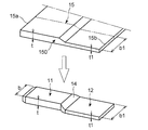
図3に示す工程においては、一方の側縁寄りの部分が板厚tをなし、他方の側縁寄りの部分が板厚t1をなす形状に研削若しくは切削加工された長尺の条材150を原材料として回路基板用端子10(図1参照)を形成する。条材150を板幅b1のサイズに切断して得られる帯板状の金属板15において、板厚tの基端部15a側で嵌合部11が形成され、板厚t1の先端部15b側で端子部12が形成される。嵌合部11と端子部12との間には、板厚tから板厚t1に連続的に減少するとともに、板幅bが板幅b1に連続的に増大する境界部14が形成される。この後、端子部12にその板厚t1方向に撓んだ複数の折曲部13を設ければ、図1に示す回路基板用端子10が完成する。
In the process shown in FIG. 3, a
図3に示す工程は、多種多様な形状の回路基板用端子を製作することが可能であり、完成後の寸法の精度が高い点において優れている。 The process shown in FIG. 3 is excellent in that the circuit board terminals of various shapes can be manufactured, and the accuracy of the dimensions after completion is high.
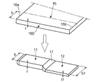
図4に示す工程においては、板厚tの長尺の条材160を板幅bのサイズに切断して得られる帯板状の金属板16の略中央から基端部16a寄りの領域は加工することなく嵌合部11とし、前記略中央から先端部16b寄りの領域をプレス圧延加工して板厚t1及び板幅b1とすることによって端子部12を形成している。また、嵌合部11と端子部12との間には、板厚tが板厚t1に連続的に減少し、板幅bが板幅b1に連続的に増大する境界部17が形成されている。この後、端子部12にその板厚t1方向に撓んだ複数の折曲部13を設ければ、図1に示す回路基板用端子10が完成する。
In the process shown in FIG. 4, the region near the
図4に示す工程は、板厚が一定の条材160を使用するので材料コストが安く、材料の損失が少なく、加工時間が短く生産性が高く、安定した精度で量産することが可能である点において優れている。
The process shown in FIG. 4 uses a
次に、図5,図6に基づいて、本発明の第2実施形態である回路基板用端子20について説明する。
Next, the
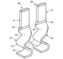
図5に示すように、回路基板用端子20は、絶縁ハウジング(図示せず)に固定される嵌合部21と、回路基板(図示せず)に接合するため嵌合部21から延設された端子部22とを有する帯板状の部材であり、端子部22の板厚t1を嵌合部21の板厚tより小とし、端子部22の板幅b1を嵌合部21の板幅bより大としている。また、端子部22にその板厚方向t1に撓んだ複数の折曲部23を設けるとともに、嵌合部21と端子部22との間に、それぞれの板幅b,b1方向が、嵌合部21の仮想軸線21cを中心に相対的に90度回転変位した捻転部25を設けている。
As shown in FIG. 5, the
また、図5に示すように、嵌合部21と捻転部25との間には、板厚tが板厚t1に連続的に減少するとともに、板幅bが板幅b1に連続的に増大する境界部24が形成されている。端子部22の先端に位置する接合部26の、嵌合部21の板幅b方向の幅26gは板幅bより小となるように形成されている。
Further, as shown in FIG. 5, between the
回路基板用端子20は、嵌合部21の仮想軸線21cを中心にして、嵌合部21と端子部22とを相対的に逆方向に90度捻った形状であり、接合部26の幅26gは、嵌合部21の板幅bよりも小であるため、図6に示すように複数の回路基板用端子20を並列配置して使用する場合、嵌合部21の板幅bより端子部22の板幅b1を大きくした場合に生じる、回路基板用端子20の配置間隔の増大を回避することができる。
The
回路基板用端子20の捻転部25においては、嵌合部21と端子部22とが仮想軸線21cを中心にして、相対的に90度回転変位しているが、変位角度はこれに限定しないので、使用条件、例えば、回路基板用端子20の配置間隔などに応じて任意に設定することができる。
In the twisted
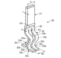
次に、図7に基づいて、本発明の第3実施形態である回路基板用端子30について説明する。図7に示すように、回路基板用端子30は、電気回路用コネクタの絶縁ハウジング1(図2参照)に固定される嵌合部31と、回路基板2(図2参照)に接合するため嵌合部31から延設された端子部32とを有する略帯板状の部材である。
Next, a
回路基板用端子30においては、端子部32の板厚t1を嵌合部32の板厚tより小とし、端子部32の嵌合部31側の板幅b3を嵌合部31の板幅bより大とし、端子部32に、その板幅b2方向と交差する複数のスリットs1,s2を開設することにより複数の櫛状の端子片32a,32b,32cを設けている。端子片32a,32b,32cにはそれぞれ板厚t1方向に撓んだ折曲部33a,33b,33cが設けられ、端子部32の板幅b2方向の両側に位置する端子片32a,32cの先端部32u,32wを互いに接近するように変位させている。また、隣り合う端子片32a,32b,32cの先端部32u,32v,32wは、交互に反対を向く方向に撓ませている。
In the
図7に示す回路基板用端子30においては、端子部32の板厚t1を嵌合部31の板厚tより小さくすることによって生じる横断面の面積の減少を、端子部32の嵌合部31側の板幅b3を嵌合部31の板幅bより大きくすることによって回避することができるので、通電時の発熱量を抑制することができる。また、端子片32a,32b,32cにそれぞれ設けられた折曲部33a,33b,33cにより、熱変形に伴って発生する応力を緩和することができるので、半田付けのクラック発生を防止することができる。さらに、端子部32に複数の櫛状の端子片32a,32b,32cを設けたことにより、端子部32全体の表面積が広がり放熱性が高まるため、半田付けのクラック発生を防止する上で有効である。
In the
また、回路基板用端子30においては、両側に位置する端子片32a,32cの先端部32u,32w同士の間隔を狭めることにより、先端部32u,32wの並列部分で形成される板幅b2を、端子部32の嵌合部31側の板幅b3と略同等若しくはそれより小さくすることができる。従って、複数の回路基板用端子30を並列配置して使用する場合、嵌合部31の板幅bよりも、嵌合部31側の端子部32の板幅b3を大きくしたことによって生じる、端子配置間隔の増大を回避することができる。
Further, in the
さらに、端子片32a,32b,32cにおいては、隣り合う先端部32u,32v,32wが交互に反対を向く方向に撓ませたことにより、隣り合う先端部32u,32v,32w同士が重なり合うことを回避しながら、隣り合う先端部32u,32v,32w同士の間隔を狭めることができるため、両側に位置する先端部32u,32wの並列部分で形成される板幅b2の極小化を図ることができる。
Further, in the
本発明の回路基板用端子は、比較的大電流が流れるパワー回路用コネクタの構成部品などとして、自動車産業、各種電気機器産業の分野において広く利用することができる。 The circuit board terminal of the present invention can be widely used in the fields of the automobile industry and various electrical equipment industries as a component of a power circuit connector through which a relatively large current flows.
1 絶縁ハウジング
2 回路基板
3 回路パターン
4 半田付け
10,20,30 回路基板用端子
11,21,31 嵌合部
12,22,32 端子部
13,23,33a,33b,33c 折曲部
14,17,24 境界部
15,16 金属板
15a,16a 基端部
15b,16b 先端部
21c 仮想軸線
25 捻転部
26 接合部
26g 幅
32a,32b,32c 端子片
32u,32v,32w 先端部
150,160 条材
t,t1 板厚
b,b1,b2,b3 板幅
s1,s2 スリット
DESCRIPTION OF
Claims (5)
Priority Applications (1)
| Application Number | Priority Date | Filing Date | Title |
|---|---|---|---|
| JP2011072783A JP5077458B2 (en) | 2011-03-29 | 2011-03-29 | Circuit board terminal |
Applications Claiming Priority (1)
| Application Number | Priority Date | Filing Date | Title |
|---|---|---|---|
| JP2011072783A JP5077458B2 (en) | 2011-03-29 | 2011-03-29 | Circuit board terminal |
Publications (2)
| Publication Number | Publication Date |
|---|---|
| JP2012209075A JP2012209075A (en) | 2012-10-25 |
| JP5077458B2 true JP5077458B2 (en) | 2012-11-21 |
Family
ID=47188653
Family Applications (1)
| Application Number | Title | Priority Date | Filing Date |
|---|---|---|---|
| JP2011072783A Expired - Fee Related JP5077458B2 (en) | 2011-03-29 | 2011-03-29 | Circuit board terminal |
Country Status (1)
| Country | Link |
|---|---|
| JP (1) | JP5077458B2 (en) |
Families Citing this family (5)
| Publication number | Priority date | Publication date | Assignee | Title |
|---|---|---|---|---|
| JP7454982B2 (en) * | 2020-03-30 | 2024-03-25 | 新電元工業株式会社 | Connection terminals and electronic devices |
| JP7600504B2 (en) * | 2020-12-28 | 2024-12-17 | ヒロセ電機株式会社 | Electrical Connectors |
| JP7711548B2 (en) * | 2021-10-19 | 2025-07-23 | オムロン株式会社 | electromagnetic relay |
| CN116365268A (en) * | 2021-12-28 | 2023-06-30 | 捷拓科技股份有限公司 | Terminal for connecting a plurality of terminals |
| JP7792065B2 (en) * | 2022-06-09 | 2025-12-25 | 株式会社オートネットワーク技術研究所 | Terminal fittings |
Family Cites Families (1)
| Publication number | Priority date | Publication date | Assignee | Title |
|---|---|---|---|---|
| US5167513A (en) * | 1991-08-14 | 1992-12-01 | International Business Machines Corp. | Load limited pin for an electrical connector |
-
2011
- 2011-03-29 JP JP2011072783A patent/JP5077458B2/en not_active Expired - Fee Related
Also Published As
| Publication number | Publication date |
|---|---|
| JP2012209075A (en) | 2012-10-25 |
Similar Documents
| Publication | Publication Date | Title |
|---|---|---|
| JP6413096B2 (en) | Coil parts | |
| JP5298336B2 (en) | Shunt resistor and manufacturing method thereof | |
| JP5077458B2 (en) | Circuit board terminal | |
| JP6167294B2 (en) | Coil parts | |
| CN102842794A (en) | Contact and socket | |
| JP5939706B2 (en) | Busba | |
| JP2005353567A (en) | Press-fit terminal and circuit board module using the same | |
| JP2011077022A (en) | Board terminal | |
| JP6124953B2 (en) | Double-thick double-ended male blade terminal and manufacturing method thereof | |
| JP6827019B2 (en) | Press-fit terminals and board assembly | |
| JP4844512B2 (en) | Terminal fixing structure for electrically connecting circuit board and wiring conductor, and terminal fixing method for electrically connecting circuit board and wiring conductor | |
| WO2016167095A1 (en) | Press-fit terminal and substrate connector | |
| JP7567261B2 (en) | Current Detector | |
| JP5622051B2 (en) | Board terminal and board connector using the same | |
| JP6307365B2 (en) | Terminal, terminal mounting structure, and electrical junction box comprising said terminal | |
| JP5816065B2 (en) | Connected body | |
| JP2013125581A (en) | Electric connector | |
| JP2010123618A (en) | Printed circuit board provided with component with terminal | |
| JP5151936B2 (en) | Terminal fitting and manufacturing method thereof | |
| CN100479263C (en) | Grounding end and electronic equipment having the same | |
| CN203326170U (en) | Conductive terminal | |
| JP6440468B2 (en) | Crimp terminal | |
| JP7486037B2 (en) | Flexible printed circuit board connection structure and method for manufacturing flexible printed circuit board unit | |
| JP2011253991A (en) | Printed board laminating body | |
| JP2019517711A (en) | Electrical connection assembly with heavily bent soldering pins |
Legal Events
| Date | Code | Title | Description |
|---|---|---|---|
| TRDD | Decision of grant or rejection written | ||
| A01 | Written decision to grant a patent or to grant a registration (utility model) |
Free format text: JAPANESE INTERMEDIATE CODE: A01 Effective date: 20120731 |
|
| A01 | Written decision to grant a patent or to grant a registration (utility model) |
Free format text: JAPANESE INTERMEDIATE CODE: A01 |
|
| A61 | First payment of annual fees (during grant procedure) |
Free format text: JAPANESE INTERMEDIATE CODE: A61 Effective date: 20120813 |
|
| FPAY | Renewal fee payment (event date is renewal date of database) |
Free format text: PAYMENT UNTIL: 20150907 Year of fee payment: 3 |
|
| R150 | Certificate of patent or registration of utility model |
Ref document number: 5077458 Country of ref document: JP Free format text: JAPANESE INTERMEDIATE CODE: R150 Free format text: JAPANESE INTERMEDIATE CODE: R150 |
|
| R250 | Receipt of annual fees |
Free format text: JAPANESE INTERMEDIATE CODE: R250 |
|
| R250 | Receipt of annual fees |
Free format text: JAPANESE INTERMEDIATE CODE: R250 |
|
| R250 | Receipt of annual fees |
Free format text: JAPANESE INTERMEDIATE CODE: R250 |
|
| R250 | Receipt of annual fees |
Free format text: JAPANESE INTERMEDIATE CODE: R250 |
|
| R250 | Receipt of annual fees |
Free format text: JAPANESE INTERMEDIATE CODE: R250 |
|
| R250 | Receipt of annual fees |
Free format text: JAPANESE INTERMEDIATE CODE: R250 |
|
| LAPS | Cancellation because of no payment of annual fees |