JP6124953B2 - Double-thick double-ended male blade terminal and manufacturing method thereof - Google Patents
Double-thick double-ended male blade terminal and manufacturing method thereof Download PDFInfo
- Publication number
- JP6124953B2 JP6124953B2 JP2015132463A JP2015132463A JP6124953B2 JP 6124953 B2 JP6124953 B2 JP 6124953B2 JP 2015132463 A JP2015132463 A JP 2015132463A JP 2015132463 A JP2015132463 A JP 2015132463A JP 6124953 B2 JP6124953 B2 JP 6124953B2
- Authority
- JP
- Japan
- Prior art keywords
- blade
- thickness
- electrical terminal
- terminal
- electrical
- Prior art date
- Legal status (The legal status is an assumption and is not a legal conclusion. Google has not performed a legal analysis and makes no representation as to the accuracy of the status listed.)
- Active
Links
- 238000004519 manufacturing process Methods 0.000 title claims description 9
- 238000000034 method Methods 0.000 claims description 20
- 238000004049 embossing Methods 0.000 claims description 14
- 239000000758 substrate Substances 0.000 claims description 11
- 239000004020 conductor Substances 0.000 claims description 8
- 230000013011 mating Effects 0.000 description 11
- 239000000463 material Substances 0.000 description 7
- RYGMFSIKBFXOCR-UHFFFAOYSA-N Copper Chemical compound [Cu] RYGMFSIKBFXOCR-UHFFFAOYSA-N 0.000 description 5
- 229910052802 copper Inorganic materials 0.000 description 5
- 239000010949 copper Substances 0.000 description 5
- 229910052751 metal Inorganic materials 0.000 description 3
- 239000002184 metal Substances 0.000 description 3
- 229910001369 Brass Inorganic materials 0.000 description 2
- 229910000881 Cu alloy Inorganic materials 0.000 description 2
- DMFGNRRURHSENX-UHFFFAOYSA-N beryllium copper Chemical compound [Be].[Cu] DMFGNRRURHSENX-UHFFFAOYSA-N 0.000 description 2
- 239000010951 brass Substances 0.000 description 2
- 238000009434 installation Methods 0.000 description 2
- 238000004080 punching Methods 0.000 description 2
- ZMHWQAHZKUPENF-UHFFFAOYSA-N 1,2-dichloro-3-(4-chlorophenyl)benzene Chemical compound C1=CC(Cl)=CC=C1C1=CC=CC(Cl)=C1Cl ZMHWQAHZKUPENF-UHFFFAOYSA-N 0.000 description 1
- LVROLHVSYNLFBE-UHFFFAOYSA-N 2,3,6-trichlorobiphenyl Chemical compound ClC1=CC=C(Cl)C(C=2C=CC=CC=2)=C1Cl LVROLHVSYNLFBE-UHFFFAOYSA-N 0.000 description 1
- ATJFFYVFTNAWJD-UHFFFAOYSA-N Tin Chemical compound [Sn] ATJFFYVFTNAWJD-UHFFFAOYSA-N 0.000 description 1
- 229910045601 alloy Inorganic materials 0.000 description 1
- 239000000956 alloy Substances 0.000 description 1
- 238000013459 approach Methods 0.000 description 1
- 239000000919 ceramic Substances 0.000 description 1
- MPTQRFCYZCXJFQ-UHFFFAOYSA-L copper(II) chloride dihydrate Chemical compound O.O.[Cl-].[Cl-].[Cu+2] MPTQRFCYZCXJFQ-UHFFFAOYSA-L 0.000 description 1
- 238000005260 corrosion Methods 0.000 description 1
- 230000007797 corrosion Effects 0.000 description 1
- 238000005520 cutting process Methods 0.000 description 1
- 238000010586 diagram Methods 0.000 description 1
- 239000003822 epoxy resin Substances 0.000 description 1
- 239000004744 fabric Substances 0.000 description 1
- 239000000835 fiber Substances 0.000 description 1
- 239000003365 glass fiber Substances 0.000 description 1
- 238000003780 insertion Methods 0.000 description 1
- 230000037431 insertion Effects 0.000 description 1
- 239000002648 laminated material Substances 0.000 description 1
- 238000012423 maintenance Methods 0.000 description 1
- 239000007769 metal material Substances 0.000 description 1
- 150000003071 polychlorinated biphenyls Chemical class 0.000 description 1
- 229920000647 polyepoxide Polymers 0.000 description 1
- 229920001721 polyimide Polymers 0.000 description 1
- 239000009719 polyimide resin Substances 0.000 description 1
- 229920000642 polymer Polymers 0.000 description 1
- 239000011253 protective coating Substances 0.000 description 1
- 239000011347 resin Substances 0.000 description 1
- 229920005989 resin Polymers 0.000 description 1
- 229910000679 solder Inorganic materials 0.000 description 1
- 238000005476 soldering Methods 0.000 description 1
Images


Classifications
-
- H—ELECTRICITY
- H01—ELECTRIC ELEMENTS
- H01R—ELECTRICALLY-CONDUCTIVE CONNECTIONS; STRUCTURAL ASSOCIATIONS OF A PLURALITY OF MUTUALLY-INSULATED ELECTRICAL CONNECTING ELEMENTS; COUPLING DEVICES; CURRENT COLLECTORS
- H01R13/00—Details of coupling devices of the kinds covered by groups H01R12/70 or H01R24/00 - H01R33/00
- H01R13/02—Contact members
- H01R13/04—Pins or blades for co-operation with sockets
-
- H—ELECTRICITY
- H01—ELECTRIC ELEMENTS
- H01R—ELECTRICALLY-CONDUCTIVE CONNECTIONS; STRUCTURAL ASSOCIATIONS OF A PLURALITY OF MUTUALLY-INSULATED ELECTRICAL CONNECTING ELEMENTS; COUPLING DEVICES; CURRENT COLLECTORS
- H01R12/00—Structural associations of a plurality of mutually-insulated electrical connecting elements, specially adapted for printed circuits, e.g. printed circuit boards [PCB], flat or ribbon cables, or like generally planar structures, e.g. terminal strips, terminal blocks; Coupling devices specially adapted for printed circuits, flat or ribbon cables, or like generally planar structures; Terminals specially adapted for contact with, or insertion into, printed circuits, flat or ribbon cables, or like generally planar structures
- H01R12/50—Fixed connections
- H01R12/51—Fixed connections for rigid printed circuits or like structures
- H01R12/55—Fixed connections for rigid printed circuits or like structures characterised by the terminals
- H01R12/58—Fixed connections for rigid printed circuits or like structures characterised by the terminals terminals for insertion into holes
- H01R12/585—Terminals having a press fit or a compliant portion and a shank passing through a hole in the printed circuit board
-
- H—ELECTRICITY
- H01—ELECTRIC ELEMENTS
- H01R—ELECTRICALLY-CONDUCTIVE CONNECTIONS; STRUCTURAL ASSOCIATIONS OF A PLURALITY OF MUTUALLY-INSULATED ELECTRICAL CONNECTING ELEMENTS; COUPLING DEVICES; CURRENT COLLECTORS
- H01R43/00—Apparatus or processes specially adapted for manufacturing, assembling, maintaining, or repairing of line connectors or current collectors or for joining electric conductors
- H01R43/16—Apparatus or processes specially adapted for manufacturing, assembling, maintaining, or repairing of line connectors or current collectors or for joining electric conductors for manufacturing contact members, e.g. by punching and by bending
-
- B—PERFORMING OPERATIONS; TRANSPORTING
- B60—VEHICLES IN GENERAL
- B60R—VEHICLES, VEHICLE FITTINGS, OR VEHICLE PARTS, NOT OTHERWISE PROVIDED FOR
- B60R16/00—Electric or fluid circuits specially adapted for vehicles and not otherwise provided for; Arrangement of elements of electric or fluid circuits specially adapted for vehicles and not otherwise provided for
- B60R16/02—Electric or fluid circuits specially adapted for vehicles and not otherwise provided for; Arrangement of elements of electric or fluid circuits specially adapted for vehicles and not otherwise provided for electric constitutive elements
- B60R16/023—Electric or fluid circuits specially adapted for vehicles and not otherwise provided for; Arrangement of elements of electric or fluid circuits specially adapted for vehicles and not otherwise provided for electric constitutive elements for transmission of signals between vehicle parts or subsystems
- B60R16/0238—Electrical distribution centers
-
- H—ELECTRICITY
- H01—ELECTRIC ELEMENTS
- H01R—ELECTRICALLY-CONDUCTIVE CONNECTIONS; STRUCTURAL ASSOCIATIONS OF A PLURALITY OF MUTUALLY-INSULATED ELECTRICAL CONNECTING ELEMENTS; COUPLING DEVICES; CURRENT COLLECTORS
- H01R13/00—Details of coupling devices of the kinds covered by groups H01R12/70 or H01R24/00 - H01R33/00
- H01R13/02—Contact members
- H01R13/04—Pins or blades for co-operation with sockets
- H01R13/05—Resilient pins or blades
- H01R13/055—Resilient pins or blades co-operating with sockets having a rectangular transverse section
Landscapes
- Engineering & Computer Science (AREA)
- Manufacturing & Machinery (AREA)
- Coupling Device And Connection With Printed Circuit (AREA)
- Manufacturing Of Electrical Connectors (AREA)
- Structures For Mounting Electric Components On Printed Circuit Boards (AREA)
Description
本願は、2014年7月2日に出願された米国特許出願第14/321,922号の優先権を主張するものである。出典を明示することにより、この出願に開示された全ての内容は本明細書の開示の一部とされる。 This application claims priority from US patent application Ser. No. 14 / 321,922, filed Jul. 2, 2014. By specifying the source, all contents disclosed in this application are made part of the disclosure of this specification.
本発明は、全体として電気端子に関し、更に詳細には、一方のブレードの厚さが他方のブレードの厚さと異なるダブルエンド雄型ブレード端子に関する。 The present invention relates generally to electrical terminals, and more particularly to a double-ended male blade terminal in which the thickness of one blade is different from the thickness of the other blade.
自動車では、様々な電気回路を相互接続するために電気センタが使用されている。電気センタは、車輛の配線をリレー等の回路切り換えデバイス及びヒューズ等の回路保護デバイスに接続する、多数の電気ワイヤハーネスコネクタを含む。 In automobiles, electrical centers are used to interconnect various electrical circuits. The electrical center includes a number of electrical wire harness connectors that connect vehicle wiring to circuit switching devices such as relays and circuit protection devices such as fuses.
様々な機能及び位置に対してケーブルを介して接続を提供する金属製端子に接続された銅製の経路/トレースを通して電子部品を機械的に支持し、電気的に接続するのにプリント回路基板(PCB)が使用されている。PCB端子は、電子デバイス(例えばヒューズ及びリレー)の機械的支持体として使用され、これらのデバイスとワイヤハーネスコネクタとの間を電気的に接続する。代表的には、電気センタは、ワイヤハーネスコネクタがPCBの一方の側に纏められ、電子デバイスが他方の側に纏められるように設計されている。 A printed circuit board (PCB) for mechanically supporting and electrically connecting electronic components through copper paths / traces connected to metal terminals that provide connections via cables for various functions and locations ) Is used. The PCB terminal is used as a mechanical support for electronic devices (eg, fuses and relays) and provides an electrical connection between these devices and the wire harness connector. Typically, the electrical center is designed such that the wire harness connector is grouped on one side of the PCB and the electronic device is grouped on the other side.
PCBは、代表的には、両面に銅が予め適用された積層材料として購入される。望ましからぬ銅を様々な方法で除去し、所望の銅トレースだけを残す。様々な電気搬送性能の回路を受け入れるため、銅の厚さが様々な幾つかのPCBを使用し、コンパクトな立体的電気センタ又は同様の構成要素を経済的に形成するのが望ましい。 The PCB is typically purchased as a laminated material in which copper is previously applied to both sides. Undesired copper is removed in various ways, leaving only the desired copper trace. In order to accept circuits of varying electrical transport performance, it is desirable to use several PCBs with varying copper thicknesses to economically form compact three-dimensional electrical centers or similar components.
装着される電気部品並びに必要な電流容量で決まる様々な厚さ及び幅を持つように設計された多くのPCB端子がある。全ての電子デバイス(ヒューズ、リレー、等)は、これらのデバイスが装着される特定の相手側端子(音叉/雌端子又は雄ブレード)の厚さ標準として設計されている。これらの電子デバイスの幾つかの端子は、0.8mm乃至1.2mm厚の金属素材である。電子デバイスが特定の厚さのブレードを必要とし、機能に対する接続を供給するワイヤに接続する出力雌ソケット端子が電子デバイスと異なる厚さを必要とする場合には、代表的には、二つの別々の端子をPCBに配置し、これらを導電性トレースによって接続する。これは、PCBで空間を必要とし、必要とされるPCB層の数が増大し、これによって製造に要する組み立て時間及び費用、端子の数、材料(例えばハンダ及び/又は絶縁保護コーティング)が増大し、おそらくは電気センタの寸法が増大する。 There are a number of PCB terminals designed to have varying thicknesses and widths depending on the electrical components to be mounted and the required current capacity. All electronic devices (fuses, relays, etc.) are designed as a thickness standard for the specific mating terminal (tuning fork / female terminal or male blade) to which these devices are attached. Some terminals of these electronic devices are 0.8 mm to 1.2 mm thick metal material. If the electronic device requires a specific thickness of blade and the output female socket terminal connected to the wire that provides the connection for the function requires a different thickness than the electronic device, typically two separate Are placed on the PCB and connected by conductive traces. This requires space on the PCB and increases the number of PCB layers required, which increases the assembly time and cost required for manufacturing, the number of terminals, and materials (eg, solder and / or insulating protective coating). Perhaps the size of the electrical center increases.
従来技術で論じた要旨は、単に従来技術で言及されたことを以て従来技術であると仮定されるべきではない。同様に、従来技術及び従来技術の要旨と関連して言及された問題は、従来技術でこれまでに認識されたものであると仮定されるべきではない。従来技術の要旨は、備わる本質に関して本発明でもある様々なアプローチを提示したに過ぎない。 The subject matter discussed in the prior art should not be assumed to be prior art simply by reference to the prior art. Similarly, the problems mentioned in connection with the prior art and the gist of the prior art should not be assumed to have been previously recognized in the prior art. The gist of the prior art only presents various approaches that are also the present invention with respect to the nature of the prior art.
本発明の一実施例によれば、ダブルエンド雄型ブレード電気端子が提供される。ダブルエンド雄型ブレード電気端子は、実質的に均等な第1厚さを特徴とする第1ブレードと、第1厚さよりも大きい実質的に均等な第2厚さを特徴とする、エンボス加工を施した中央領域を持つ第2ブレードとを含む。一つの特定の実施例によれば、第1厚さは約0.8mmであり、第2厚さは約1.2mmである。第1ブレードの一方の側及び第2ブレードの一方の側は、実質的に同一平面内にあってもよい。電気端子は、第1ブレードと、第2ブレードとの中間に肩部を形成してもよい。肩部は、第1ブレード幅及び第2ブレード幅よりも大きい肩部幅を有する。 According to one embodiment of the present invention, a double-ended male blade electrical terminal is provided. The double-ended male blade electrical terminal is embossed, characterized by a first blade characterized by a substantially uniform first thickness and a substantially uniform second thickness greater than the first thickness. And a second blade having an applied central region. According to one particular embodiment, the first thickness is about 0.8 mm and the second thickness is about 1.2 mm. One side of the first blade and one side of the second blade may be substantially in the same plane. The electrical terminal may form a shoulder portion between the first blade and the second blade. The shoulder has a shoulder width greater than the first blade width and the second blade width.
第1ブレードの第1遠位端及び第2ブレードの第2遠位端には傾斜面(又は面取り)を施してもよい。第2遠位端と近接したエンボス領域の前端は、丸みを帯びた二等辺三角形形状を形成し、エンボス領域の側部は、第2ブレードの側部と実質的に平行であり、エンボス領域の後端は、丸みを帯びた隅部を持つことを特徴とする。電気端子の一つの特定の実施例によれば、エンボス領域の前端の二つの側部は、電気端子の長さ方向軸線に対して30°の角度を形成し、第2ブレード幅は、第1ブレード幅よりも大きい。 An inclined surface (or chamfer) may be provided on the first distal end of the first blade and the second distal end of the second blade. The front end of the embossed region proximate to the second distal end forms a rounded isosceles triangle shape, and the side of the embossed region is substantially parallel to the side of the second blade, The rear end is characterized by a rounded corner. According to one particular embodiment of the electrical terminal, the two sides of the front end of the embossed area form an angle of 30 ° with the longitudinal axis of the electrical terminal and the second blade width is the first Greater than blade width.
本発明の別の実施例では、プリント回路基板(PCB)アッセンブリが提供される。PCBアッセンブリは、絶縁性(誘電体)基板と、基板の表面上に配置された導電性トレースと、基板によって形成された穴内に配置されたダブルエンド雄型ブレード電気端子とを含む。電気端子は、実質的に均等な第1厚さを特徴とする第1ブレードと、第1厚さよりも大きい実質的に均等な第2厚さを特徴とするエンボス加工を施した中央領域を持つ第2ブレードとを含む。電気端子は、導電性トレースとぴったりとは接触していなくてもよい。第1ブレードは、基板の第1面から突出しており、第2ブレードは、第1面とは反対側の基板の第2面から突出している。第2ブレードは、電気コネクタ内の相手側ソケット端子に接続されるように形成されており、これに対し、第1ブレードは、電気デバイス内の相手側ソケット端子に接続されるように形成されている。PCBアッセンブリの一実施例によれば、電気デバイスは、可融性(又は可溶性)のリンクを含み、別の実施例によれば、電気デバイスは、電気機械的リレーを含む。 In another embodiment of the present invention, a printed circuit board (PCB) assembly is provided. The PCB assembly includes an insulating (dielectric) substrate, conductive traces disposed on the surface of the substrate, and double-ended male blade electrical terminals disposed in holes formed by the substrate. The electrical terminal has a first blade characterized by a substantially uniform first thickness and an embossed central region characterized by a substantially uniform second thickness greater than the first thickness. A second blade. The electrical terminal may not be in close contact with the conductive trace. The first blade protrudes from the first surface of the substrate, and the second blade protrudes from the second surface of the substrate opposite to the first surface. The second blade is formed to be connected to the mating socket terminal in the electrical connector, whereas the first blade is configured to be connected to the mating socket terminal in the electrical device. Yes. According to one embodiment of the PCB assembly, the electrical device includes a fusible (or fusible) link, and according to another embodiment, the electrical device includes an electromechanical relay.
本発明の更に別の実施例では、実質的に均等な第1厚さを特徴とする第1ブレードと、第1厚さよりも大きい実質的に均等な第2厚さを特徴とする第2ブレードとを有する、ダブルエンド雄型ブレード電気端子の製造方法が提供される。方法は、実質的に均等な第1厚さの導電材料のシートからダブルエンド雄型ブレード電気端子を形成する工程と、第2ブレードの中央領域が実質的に均等な第2厚さを特徴とするように、第2ブレードの中央領域にエンボス加工を施す工程とを含む。第1ブレードの一方の側及び第2ブレードの一方の側は、実質的に同一平面内にあってもよい。電気端子は、第1ブレードと、第2ブレードとの中間に肩部を形成してもよい。前記肩部は、第1ブレード幅及び第2ブレード幅よりも大きい肩部幅を有する。一つの特定の実施例によれば、導電性シートは、約0.8mmの第1厚さを有し、中央領域は、エンボス加工により約1.2mmの第2厚さにされている。 In yet another embodiment of the present invention, a first blade characterized by a substantially uniform first thickness and a second blade characterized by a substantially uniform second thickness greater than the first thickness. A method of manufacturing a double-ended male blade electrical terminal is provided. The method features forming a double-ended male blade electrical terminal from a sheet of conductive material having a substantially uniform first thickness, and a second thickness in which a central region of the second blade is substantially uniform. And embossing the central region of the second blade. One side of the first blade and one side of the second blade may be substantially in the same plane. The electrical terminal may form a shoulder portion between the first blade and the second blade. The shoulder has a shoulder width greater than the first blade width and the second blade width. According to one particular embodiment, the conductive sheet has a first thickness of about 0.8 mm and the central region is embossed to a second thickness of about 1.2 mm.
方法は、更に、第1ブレードの第1遠位端及び第2ブレードの第2遠位端に面取り(斜面)を施す工程を含んでもよい。第2遠位端と近接したエンボス領域の前端には、丸みを帯びた二等辺三角形形状を形成するようにエンボス加工が施されていてもよい。エンボス領域の後端には、丸みを帯びた一対の隅部を形成するようにエンボス加工が施されていてもよい。エンボス領域の側部は、第2ブレードの側部と実質的に平行であってもよい。エンボス領域の前端の二つの側部は、電気端子の長さ方向軸線に対して30°の角度を形成するようにエンボス加工が施されていてもよい。一つの特定の実施例によれば、電気端子は、第2ブレード幅が第1ブレード幅よりも大きいように形成されている。 The method may further include chamfering (beveling) the first distal end of the first blade and the second distal end of the second blade. The front end of the embossed region adjacent to the second distal end may be embossed so as to form a rounded isosceles triangle shape. Embossing may be performed at the rear end of the embossed region so as to form a pair of rounded corners. The side of the embossed region may be substantially parallel to the side of the second blade. The two side portions at the front end of the embossed region may be embossed so as to form an angle of 30 ° with respect to the longitudinal axis of the electrical terminal. According to one particular embodiment, the electrical terminal is formed such that the second blade width is greater than the first blade width.
本発明のこの他の特徴及び利点は、単なる非限定的例として与えられた本発明の好ましい実施例の以下の詳細な説明を、添付図面を参照して読むことにより、更に明瞭に理解されるであろう。 Other features and advantages of the present invention will be more clearly understood from the following detailed description of a preferred embodiment of the invention given by way of non-limiting example only, with reference to the accompanying drawings, in which: Will.
次に、本発明を、添付図面を参照して例として説明する。 The present invention will now be described by way of example with reference to the accompanying drawings.
ダブルエンド雄型ブレード電気端子を以下に説明する。端子は、有効厚さが異なる二つの端子ブレードを有する。電気端子は、車輛の電気センタのプリント回路基板で使用するのに適している。端子の第1ブレードは第1厚さを有し、PCBの一方の側で車輛のワイヤハーネスの相手側ソケットコネクタに接続するのに使用されてもよいが、PCBの他方の側の異なる第2厚さの第2ブレードは、リレーのヒューズ等の電気デバイスのソケットコネクタに直接的に差し込まれてもよい。この端子により、厚さが異なる二つの別々のブレード端子に対する必要をなくし、これらの取り付け及び接続に必要なPCB占有面積及び導電性トレースを減少する。 A double-ended male blade electrical terminal is described below. The terminal has two terminal blades with different effective thicknesses. The electrical terminals are suitable for use on a printed circuit board in a vehicle electrical center. The first blade of the terminal has a first thickness and may be used to connect to the mating socket connector of the vehicle wire harness on one side of the PCB, but a different second on the other side of the PCB. The second blade of thickness may be plugged directly into a socket connector of an electrical device such as a relay fuse. This terminal eliminates the need for two separate blade terminals of different thickness and reduces the PCB footprint and conductive traces required for their installation and connection.
図1は、自動車(図示せず)で使用するように形成された電気センタ10の非限定的例を示す。電気センタは、プリント回路基板(PCB)アッセンブリ14を収容したハウジング12を含む。PCBアッセンブリ14は、リレー又はヒューズ等の電子デバイス16を接続するように形成された導電性トレース(図示せず)と、これらの導電性トレースに接続されていてもよいし、接続されていなくてもよい電気端子(図示せず)とを含む。PCBは、エポキシ樹脂やポリイミド樹脂から形成されていてもよい。樹脂は、ガラス繊維織物又はチョップドファイバ等の他の母材で強化されていてもよい。このような材料で形成されたPCBは、代表的には、FR−4型回路基板又はG−10型回路基板と呼ばれる。PCBは、別の態様では、セラミックや硬質ポリマーで形成されていてもよい。ここで言及した受容可能なPCB材料は網羅的ではなく、他の材料も十分に使用される。プリント回路基板の形成に使用された材料及び製造技術は、当業者に周知である。電気センタは、更に、電子デバイスの設置及び保守に必要な電子デバイスへのアクセスを行うことができるように、上から取り外すことができるカバー18を含む。電子デバイスは、PCBの一方の側20に配置されており、電気センタ10を車輛のワイヤハーネスコネクタに相互接続するように形成された電気端子が、PCBの反対側22に配置されている。
FIG. 1 shows a non-limiting example of an
図2は、PCBアッセンブリ14の非限定的例を断面で示す。第1雌ソケット端子24を持つヒューズ等の電子デバイス16が、PCBの穴32即ち「バイア(via)」を通して取り付けられたダブルエンド雄型ブレード端子30によって、ワイヤハーネスコネクタ28の別の雌ソケット端子26に直接的に接続されている。第1ブレード40がPCBの第1面20から突出しており、第2ブレード42が、第1面20とは反対側のPCBの第2面22から突出している。電子デバイス16の第2ソケット端子34が、PCBの第1面20に取り付けられたシングルエンド雄型ブレード端子36に接続されている。ダブルエンド雄型ブレード端子30及びシングルエンド雄型ブレード端子36は、両方とも、銅合金、真鍮、又はベリリウム銅等の導電材料で形成されている。ダブルエンド端子30及びシングルエンド端子36には、耐蝕性を提供するため、例えば錫を基材とした合金でめっきが施されていてもよい。図2に示す例では、ダブルエンド端子30はPCBトレースに接続されていないが、シングルエンド端子36はPCBトレース38に接続されている。ダブルエンド雄型ブレード端子がPCBの導電性トレースに接続された、PCBアッセンブリの変形例が考えられる。
FIG. 2 shows a non-limiting example of the
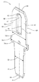
図4Dに示すように、電子デバイス16の第1雌ソケット端子24に接続されたダブルエンド端子30の第1ブレード40は、実質的に均等な第1厚さT1を有する。第1厚さT1は、例示の例によれば、約0.8mm(0.8+0.052/−0.000mm)である。本明細書中で使用したように、実質的に均等な厚さは、±0.026mmである。ワイヤハーネスコネクタ28の雌ソケット端子26に接続されるように形成されたダブルエンド端子30の第2ブレード42は、第2ブレード42の中央部に領域44を有する。この領域では、第2ブレード42にはエンボス加工が施されており、又は第2ブレード42の周囲の材料から盛り上がっている。このエンボス領域44は、第2ブレード42の有効厚さを実質的に均等な第2厚さT2に増大する。第2厚さT2は、例示の例によれば、約1.2mm(1.2±0.026mm)であり、第1厚さT1よりも大きい。本明細書中で使用したように、エンボス加工を施したというのは、第2ブレード42の第1側46が突出領域48を持ち、第1側46とは反対側の第2側50が対応する窪み領域52を形成するように、第2ブレード42をパンチ、ダイ、又は他の金属変形プロセスによって変形したということを意味する。
As shown in FIG. 4D, the
図4B及び図4Cに最もよく示すように、エンボス領域44は、第2ブレード42の第1側46及び第2側50と実質的に平行な平らな部分54を含む。本明細書中で使用したように、実質的に平行なというのは、平らな部分54が、絶対平行状態の±10°にあるということを意味する。第1ブレード40の第2側は、第2ブレード42の第2側と実質的に同一平面内にある。本明細書中で使用したように、実質的に同一平面内にあるというのは、第1ブレード40の第2側が、絶対的に同一平面内にある状態から±5°及び±0.5mmにあるということを意味する。第2厚さT2は、第2ブレード42の第1側からエンボス領域44の平らな部分54までの距離である。エンボス領域44は実質的に非可曲性(non-compliant)であり、第2ブレード42に連続的に取り付けられている。本明細書中で使用したように、実質的に非可曲性というのは、通常の作業で相手側ソケットコネクタによって及ぼされた力でエンボス領域44が変形しないということを意味する。エンボス領域44は、円弧状固定ビーム又は片持ち梁としての特徴を備えていない。エンボス領域44は、対応する相手側ソケット端子26にばね力を及ぼすようには形成されておらず、というよりはむしろ、対応する相手側ソケット端子26が、エンボス領域44を含む第2ブレード42にばね力を及ぼすように形成されている。
As best shown in FIGS. 4B and 4C, the embossed
図4A及び図4Dに最もよく示すように、第1ブレード40の先端の第1遠位端56及び第2ブレード42の先端の第2遠位端58には、対応する相手側ソケット端子24、26へのブレード40、42の挿入を容易にするため、ブレード40、42の厚さT1及び幅W1、W2を小さくするように、角度をなした面取り(斜面)が施してある。
As best shown in FIGS. 4A and 4D, the first
図4Aに示すように、エンボス領域44の前端60、即ち第2ブレード42の第2遠位端58と近接した、即ちこれに最も近い端部は、丸みを帯びた二等辺三角形形状62を形成する。例示の例では、エンボス領域44の前端60の二つの側部64は、ダブルエンド端子30の長さ方向軸線Aに対して30°の角度を形成する。前端60が三角形形状62であるため、対応する相手側ソケット端子26への第2ブレード42の挿入が容易になる。エンボス領域44の側部66は、第2ブレード42の側部68と実質的に平行である。エンボス領域44の後端70は、丸みを帯びた隅部72を持つことを特徴とする。後端70の丸みを帯びた隅部72により、接続途絶中、第2ブレード42を対応する相手側ソケット端子26から容易に取り外せる。
As shown in FIG. 4A, the
次に、図3を参照すると、ダブルエンド端子30は、第1ブレード40と第2ブレード42との中間に肩部74を形成する。この肩部74の肩部幅Wsは、第1ブレード40の幅W1及び第2ブレード42の幅W2よりも大きい。例示の例によれば、第2ブレード42の幅W2は、第1ブレード40の幅W1よりも大きい。別の態様では、肩部は、第1及び第2のブレードのうちの広幅のブレードによって形成されていてもよい。電気端子の別の実施例は、第2ブレードの厚さを増大するためのエンボス領域を持つ第2ブレードよりも広幅の第1ブレードを備えていてもよく、又は第1ブレードの幅が第2ブレードと同じであってもよい。肩部74は、穴32を取り囲むPCBの銅パッドにハンダ付けプロセスで機械的に及び/又は電気的に取り付けられていてもよい。
Next, referring to FIG. 3, the
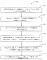
図5は、第1ブレード40が実質的に均等な第1厚さT1を有し、第2ブレード42が実質的に均等な第2厚さT2を持つという特徴を備えたダブルエンド雄型ブレード電気端子30の非限定的製造方法100を例示する。第2ブレード42の有効厚さは、第1ブレード40の厚さよりも大きい。方法100は、以下の工程を含む。
FIG. 5 shows a double-ended male blade with the feature that the
工程102、即ち実質的に均等な第1厚さの導電材料のシートからダブルエンド雄型ブレード電気端子を形成する工程は、実質的に均等な第1厚さT1の導電材料のシートからダブルエンド端子30を形成する工程を含む。ダブルエンド端子30は、銅合金、真鍮、又はベリリウム銅等の導電材料のシートから形成されてもよい。ダブルエンド端子30は、切断、打ち抜き、精密打ち抜きによって形成されてもよく、又は導電材料のシートから端子ブランクを形成する当業者に周知のこの他の任意の方法によって形成されてもよい。一つの特定の実施例によれば、シートの第1厚さT1は、約0.8mm(0.8+0.052/−0.0mm)である。第2ブレード幅W2は、第1ブレード幅W1よりも大きくてもよく、第1ブレード40の一方の側及び第2ブレード42の一方の側が実質的に同一平面内にあってもよい。
工程104、即ち第1ブレードと第2ブレードとの中間に肩部を形成する電気端子を形成する工程は、第1ブレード40と第2ブレード42との中間に肩部74を形成するようにダブルエンド電気端子30を形成する工程を含む、随意の工程である。肩部74の幅Wsは、第1ブレード幅W1及び第2ブレード幅W2よりも大きい。
工程106、即ち第1ブレードの第1遠位端及び第2ブレードの第2遠位端に面取りを施す工程は、第1ブレード40の先端の第1遠位端56及び第2ブレード42の先端の第2遠位端58に面取りを施す工程を含む、随意の工程である。
工程108、即ち第2ブレードの中央領域が第1厚さよりも大きい実質的に均等な第2厚さを持つことを特徴とするように中央領域にエンボス加工を施す工程は、エンボス加工を施した中央領域44が実質的に均等な第2厚さを持つことを特徴とするように、第2ブレード42の中央領域44にエンボス加工を施す工程を含む。エンボス領域44は、パンチ及びダイ等の従来のエンボス加工方法を使用して形成されてもよい。一つの特定の実施例によれば、エンボス領域44は、第2ブレード42の第2側からエンボス領域44の平らな部分54まで約1.2mm(1.2±0.026mm)の第2厚さを提供する。
工程110、即ち第2遠位端と近接したエンボス領域の前端にエンボス加工を施し、丸みを帯びた二等辺三角形形状を形成する工程は、第2遠位端58と近接したエンボス領域44の前端60にエンボス加工を施し、丸みを帯びた二等辺三角形形状62を形成する工程を含む。一つの特定の実施例によれば、エンボス領域44の前端60の二つの側部64は、ダブルエンド端子30の長さ方向軸線Aに対して30°の角度を形成する。
工程112、即ちエンボス領域の後端にエンボス加工を施し、丸みを帯びた一対の隅部を形成する工程は、エンボス領域44の後端70にエンボス加工を施し、丸みを帯びた一対の隅部72を形成する工程を含む。エンボス領域44の側部66は、第2ブレード42の側部68と実質的に平行である。
ダブルエンド雄型ブレード端子の例を、車輛の電気センタの部分であるPCBアッセンブリ内に示したが、車輛の電気センタ以外の用途でPCBを使用する、又は二つの相手側ソケットコネクタをPCBなしで直接的に接続するのにダブルエンド雄型ブレード端子を使用する、ダブルエンド雄型ブレード端子の他の実施例が考えられる。 An example of a double-ended male blade terminal is shown in a PCB assembly that is part of a vehicle electrical center, but the PCB is used for applications other than the vehicle electrical center, or two mating socket connectors without a PCB. Other embodiments of double-ended male blade terminals are contemplated that use double-ended male blade terminals for direct connection.
従って、PCBアッセンブリ14、ダブルエンド雄型ブレード電気端子30、及びこうした端子の製造方法100が提供される。PCBアッセンブリ14のダブルエンド端子30は、ワイヤハーネスコネクタ28の雌ソケット端子26を、ヒューズやリレー等のPCBアッセンブリ14の電子デバイス16の雌ソケット端子24に直接的に接続する利点を提供する。ワイヤハーネスコネクタ28の雌ソケット端子26は、雄型部分端子の厚さが、電気デバイスのソケット端子と異なることを必要とする。ダブルエンド端子30は、大きな「占有面積」、即ちPCBアッセンブリ14の表面20、22上の空間を必要としない。これは、二つの別々の雄型ブレード端子がPCBの各側に取り付けられており、ワイヤハーネスコネクタ28の雌ソケット端子26を電子デバイス16に相互接続するためにPCBの導電性トレースを必要としないためである。ダブルエンド端子30の製造方法100は、単一の均等な厚さの導電材料のシートから、打ち抜き及びエンボス加工等の従来の金属成形技術を使用してダブルエンド端子30を形成するという利点を提供する。
Accordingly, a
本発明をその好ましい実施例に関して説明したが、本発明はこれに限定されるものではなく、以下の特許請求の範囲の記載によってのみ限定されるものである。更に、第1、第2といった用語の使用は、その重要性を示すものではなく、第1、第2といった用語は、一つのエレメントを別のエレメントと区別するために使用されるものである。更に、単数で表現した用語は、その量を制限するものではなく、言及がなされたものが少なくとも一つあるということを意味する。 While the invention has been described in terms of its preferred embodiments, the invention is not limited thereto but only by the following claims. Furthermore, the use of terms such as “first” and “second” does not indicate their importance, and the terms “first” and “second” are used to distinguish one element from another. Further, the terms expressed in the singular are not intended to limit the amount, but mean that there is at least one mentioned.
10 電気センタ
12 ハウジング
14 プリント回路基板(PCB)アッセンブリ
16 電子デバイス
18 カバー
20 PCBの第1面
22 PCBの第2面
24 第1雌ソケット端子
26 雌ソケット端子
28 ワイヤハーネスコネクタ
30 ダブルエンド雄型ブレード端子
32 バイア
34 第2ソケット端子
36 シングルエンド雄型ブレード端子
38 PCBトレース
40 第1ブレード
42 第2ブレード
DESCRIPTION OF
Claims (17)
実質的に均等な第1厚さ(T1)を特徴とする第1ブレード(40)と、
前記第1厚さ(T1)よりも大きい実質的に均等な第2厚さ(T2)を特徴とする、エンボス加工を施した中央領域(44)を持つ第2ブレード(42)とを備え、
前記第2ブレード(42)の第2遠位端(58)と近接した前記エンボス領域(44)の前端(60)は、丸みを帯びた二等辺三角形形状(62)を形成しており、前記エンボス領域(44)の側部(66)は、前記第2ブレード(42)の側部(68)と実質的に平行であり、前記エンボス領域(44)の後端(70)は、丸みを帯びた隅部(72)を持っている、電気端子(30)。 A double-ended male blade electrical terminal (30),
A first blade (40) characterized by a substantially uniform first thickness (T1);
A second blade (42) having an embossed central region (44), characterized by a substantially equal second thickness (T2) greater than the first thickness (T1);
The front end (60) of the embossed region (44) proximate to the second distal end (58) of the second blade (42) forms a rounded isosceles triangle shape (62), The side (66) of the embossed area (44) is substantially parallel to the side (68) of the second blade (42), and the rear end (70) of the embossed area (44) is rounded. An electrical terminal (30) having a rounded corner (72).
前記第1厚さ(T1)は約0.8mmであり、前記第2厚さ(T2)は約1.2mmである、電気端子(30)。 The electrical terminal (30) according to claim 1,
The electrical terminal (30), wherein the first thickness (T1) is about 0.8 mm and the second thickness (T2) is about 1.2 mm.
前記第1ブレード(40)の一方の側及び前記第2ブレード(42)の一方の側は、実質的に同一平面上にある、電気端子(30)。 The electrical terminal (30) according to claim 1,
An electrical terminal (30), wherein one side of the first blade (40) and one side of the second blade (42) are substantially coplanar.
前記電気端子(30)は、前記第1ブレード(40)と、前記第2ブレード(42)との中間に肩部(74)を形成し、前記肩部(74)は、第1ブレード幅(W1)及び第2ブレード幅(W2)よりも大きい肩部幅(Ws)を有する、電気端子(30)。 Electrical terminal (30) according to claim 3,
The electrical terminal (30) forms a shoulder (74) between the first blade (40) and the second blade (42), and the shoulder (74) has a first blade width ( An electrical terminal (30) having a shoulder width (Ws) greater than W1) and a second blade width (W2).
前記第1ブレード(40)の第1遠位端(56)及び前記第2ブレード(42)の第2遠位端(58)には面取りが施してある、電気端子(30)。 Electrical terminal (30) according to claim 4,
An electrical terminal (30) wherein the first distal end (56) of the first blade (40) and the second distal end (58) of the second blade (42) are chamfered.
前記エンボス領域(44)の前端(60)の二つの側部(64)は、前記電気端子(30)の長さ方向軸線に対して30°の角度を形成する、電気端子(30)。 An electrical terminal (30) according to claim 5,
Two terminals (64) of the front end (60) of the embossed region (44) form an electrical terminal (30) forming an angle of 30 ° with the longitudinal axis of the electrical terminal (30).
前記第2ブレード幅(W2)は、前記第1ブレード幅(W1)よりも大きい、電気端子(30)。 Electrical terminal (30) according to claim 4,
The electrical terminal (30), wherein the second blade width (W2) is larger than the first blade width (W1).
絶縁性の基板(20)と、
前記基板(20)の表面上に配置された導電性トレース(38)と、
前記基板(20)によって形成された穴(32)内に配置されたダブルエンド雄型ブレード電気端子(30)とを備え、前記電気端子(30)は、
実質的に均等な第1厚さ(T1)を特徴とする第1ブレード(40)と、
前記第1厚さ(T1)よりも大きい実質的に均等な第2厚さ(T2)を特徴とするエンボス加工を施した中央領域(44)を持つ第2ブレード(42)とを備え、
前記第2ブレード(42)の第2遠位端(58)と近接した前記エンボス領域(44)の前端(60)は、丸みを帯びた二等辺三角形形状(62)を形成しており、前記エンボス領域(44)の側部(66)は、前記第2ブレード(42)の側部(68)と実質的に平行であり、前記エンボス領域(44)の後端(70)は、丸みを帯びた隅部(72)を持っている、PCBアッセンブリ(14)。 A printed circuit board (PCB) assembly (14) comprising:
An insulating substrate (20);
Conductive traces (38) disposed on the surface of the substrate (20);
A double-ended male blade electrical terminal (30) disposed in a hole (32) formed by the substrate (20), the electrical terminal (30) comprising:
A first blade (40) characterized by a substantially uniform first thickness (T1);
A second blade (42) having an embossed central region (44) characterized by a substantially equal second thickness (T2) greater than the first thickness (T1);
The front end (60) of the embossed region (44) proximate to the second distal end (58) of the second blade (42) forms a rounded isosceles triangle shape (62), The side (66) of the embossed area (44) is substantially parallel to the side (68) of the second blade (42), and the rear end (70) of the embossed area (44) is rounded. A PCB assembly (14) having a tinted corner (72).
前記電気端子(30)は、前記導電性トレース(38)とぴったりとは接触していない、PCBアッセンブリ(14)。 A PCB assembly (14) according to claim 8, comprising:
The PCB assembly (14), wherein the electrical terminals (30) are not in intimate contact with the conductive traces (38).
前記第1ブレード(40)は、前記基板(20)の第1面(20)から突出しており、前記第2ブレード(42)は、前記第1面(20)とは反対側の前記基板(20)の第2面(22)から突出している、PCBアッセンブリ(14)。 A PCB assembly (14) according to claim 8, comprising:
The first blade (40) protrudes from the first surface (20) of the substrate (20), and the second blade (42) is the substrate (on the opposite side to the first surface (20)). 20) a PCB assembly (14) protruding from the second surface (22).
前記第2ブレード(42)は、電気コネクタ内の相手側ソケット端子に接続されるように形成されており、前記第1ブレード(40)は、電気デバイス内の相手側ソケット端子に接続されるように形成されている、PCBアッセンブリ(14)。 A PCB assembly (14) according to claim 8, comprising:
The second blade (42) is formed to be connected to a counterpart socket terminal in an electrical connector, and the first blade (40) is connected to a counterpart socket terminal in an electrical device. A PCB assembly (14) formed on the substrate.
前記電気デバイスは、可融性のリンクを含む、PCBアッセンブリ(14)。 A PCB assembly (14) according to claim 11, comprising:
The electrical device includes a PCB assembly (14) including a fusible link.
前記電気デバイスは、電気機械的リレーを含む、PCBアッセンブリ(14)。 A PCB assembly (14) according to claim 11, comprising:
The electrical device includes a PCB assembly (14) including an electromechanical relay.
実質的に均等な第1厚さ(T1)の導電材料のシートからダブルエンド雄型ブレード電気端子(30)を形成する工程(102)と、
前記第2ブレード(42)の中央領域(44)が実質的に均等な第2厚さ(T2)を特徴とするように、前記第2ブレード(42)の中央領域(44)にエンボス加工を施す工程(108)とを含み、
前記第1ブレード(40)の一方の側及び前記第2ブレード(42)の一方の側は実質的に同一平面上にあるように形成し、
前記方法(100)は、更に、
前記第1ブレード(40)と前記第2ブレード(42)との中間に肩部(74)を形成するように前記電気端子(30)を形成する工程(104)を含み、前記肩部(74)は、第1ブレード幅(W1)及び第2ブレード幅(W2)よりも大きい肩部幅(Ws)を有するように形成し、
前記方法(100)は、更に、
前記第1ブレード(40)の第1遠位端(56)及び前記第2ブレード(42)の第2遠位端(58)に面取りを施す工程(106)と、
前記第2遠位端(58)と近接した前記エンボス領域(44)の前端(60)にエンボス加工を施し、丸みを帯びた二等辺三角形形状(62)を形成する工程(110)と、
前記エンボス領域(44)の後端(70)にエンボス加工を施し、丸みを帯びた一対の隅部72を形成する工程(112)とを備え、
前記エンボス領域(44)の側部(66)は、前記第2ブレード(42)の側部(68)と実質的に平行であるように形成される、方法(100)。 Characterized by a first blade (40) characterized by a substantially uniform first thickness (T1) and a substantially uniform second thickness (T2) greater than said first thickness (T1). A method (100) of manufacturing a double-ended male blade electrical terminal (30) having a second blade (42) that comprises:
Forming a double-ended male blade electrical terminal (30) from a sheet of conductive material having a substantially uniform first thickness (T1);
Embossing the central region (44) of the second blade (42) so that the central region (44) of the second blade (42) is characterized by a substantially uniform second thickness (T2). Applying (108),
Forming one side of the first blade (40) and one side of the second blade (42) to be substantially coplanar;
The method (100) further comprises:
Forming the electrical terminal (30) so as to form a shoulder (74) between the first blade (40) and the second blade (42), the shoulder (74) ) Is formed to have a shoulder width (Ws) larger than the first blade width (W1) and the second blade width (W2),
The method (100) further comprises:
Chamfering (106) the first distal end (56) of the first blade (40) and the second distal end (58) of the second blade (42);
Embossing the front end (60) of the embossed region (44) proximate to the second distal end (58) to form a rounded isosceles triangle shape (62);
Embossing the rear end (70) of the embossed region (44) to form a pair of rounded corners (112),
The method (100), wherein the side (66) of the embossed region (44) is formed to be substantially parallel to the side (68) of the second blade (42).
前記第1厚さ(T1)は約0.8mmであり、前記第2厚さ(T2)は約1.2mmである、方法(100)。 15. The method (100) of claim 14, wherein
The method (100), wherein the first thickness (T1) is about 0.8 mm and the second thickness (T2) is about 1.2 mm.
前記エンボス領域(44)の前端(60)の二つの側部(64)は、前記電気端子(30)の長さ方向軸線(A)に対して30°の角度を形成する、方法(100)。 15. The method (100) of claim 14 , wherein
Method (100), wherein the two sides (64) of the front end (60) of the embossed region (44) form an angle of 30 ° with respect to the longitudinal axis (A) of the electrical terminal (30). .
前記第2ブレード幅(W2)は、前記第1ブレード幅(W1)よりも大きく形成される、方法(100)。 15. The method (100) of claim 14 , wherein
The second blade width (W2), the size rather are formed than the first blade width (W1), the method (100).
Applications Claiming Priority (2)
| Application Number | Priority Date | Filing Date | Title |
|---|---|---|---|
| US14/321,922 | 2014-07-02 | ||
| US14/321,922 US9331413B2 (en) | 2014-07-02 | 2014-07-02 | Dual thickness double-ended male blade terminal |
Publications (3)
| Publication Number | Publication Date |
|---|---|
| JP2016028381A JP2016028381A (en) | 2016-02-25 |
| JP2016028381A5 JP2016028381A5 (en) | 2016-08-18 |
| JP6124953B2 true JP6124953B2 (en) | 2017-05-10 |
Family
ID=53539484
Family Applications (1)
| Application Number | Title | Priority Date | Filing Date |
|---|---|---|---|
| JP2015132463A Active JP6124953B2 (en) | 2014-07-02 | 2015-07-01 | Double-thick double-ended male blade terminal and manufacturing method thereof |
Country Status (6)
| Country | Link |
|---|---|
| US (1) | US9331413B2 (en) |
| EP (1) | EP2963739B1 (en) |
| JP (1) | JP6124953B2 (en) |
| KR (1) | KR101683386B1 (en) |
| CN (1) | CN105322330B (en) |
| BR (1) | BR102015013010A2 (en) |
Families Citing this family (5)
| Publication number | Priority date | Publication date | Assignee | Title |
|---|---|---|---|---|
| JP6183667B2 (en) * | 2015-10-01 | 2017-08-23 | 住友電装株式会社 | connector |
| US10349539B2 (en) * | 2017-10-03 | 2019-07-09 | Aptiv Technologies Limited | Vehicle electrical center and method of manufacturing same |
| EP3637564B1 (en) | 2018-10-08 | 2021-06-09 | Aptiv Technologies Limited | Process of manufacturing an electrical wiring assembly |
| CN113451808B (en) * | 2020-03-26 | 2024-01-30 | 上海莫仕连接器有限公司 | Electric connection device and terminal |
| US20210408710A1 (en) * | 2020-06-29 | 2021-12-30 | Microsoft Technology Licensing, Llc | Systems and methods for improving safety on electronic device connections |
Family Cites Families (22)
| Publication number | Priority date | Publication date | Assignee | Title |
|---|---|---|---|---|
| US2130424A (en) * | 1936-06-29 | 1938-09-20 | Albert T Otto & Sons Inc | Attachment plug |
| US2752580A (en) | 1953-04-27 | 1956-06-26 | Charles A Shewmaker | Printed circuit board and terminal connections |
| US2811702A (en) | 1956-06-21 | 1957-10-29 | Malco Tool & Mfg Co | Terminal pin for printed circuit board |
| US3977075A (en) * | 1971-10-28 | 1976-08-31 | Amp Incorporated | Method of fabricating multi-layer printed circuit board |
| JPS5968187A (en) * | 1982-10-13 | 1984-04-18 | 富士通株式会社 | Terminal structure |
| US4923414A (en) | 1989-07-03 | 1990-05-08 | E. I. Du Pont De Nemours And Company | Compliant section for circuit board contact elements |
| US5023752A (en) * | 1989-10-31 | 1991-06-11 | General Motors Corporation | Electrical power distribution center |
| US5046960A (en) * | 1990-12-20 | 1991-09-10 | Amp Incorporated | High density connector system |
| US5207603A (en) * | 1992-06-02 | 1993-05-04 | Molex Incorporated | Dual thickness blade type electrical terminal |
| DE69425829T2 (en) * | 1994-11-17 | 2001-04-26 | Molex Inc., Lisle | Self-locking contact structure |
| US5582519A (en) * | 1994-12-15 | 1996-12-10 | The Whitaker Corporation | Make-first-break-last ground connections |
| US5831814A (en) | 1997-03-14 | 1998-11-03 | General Motors Corporation | Electrical center bus plate assembly |
| US6008982A (en) * | 1998-05-20 | 1999-12-28 | General Motors Corporation | Low profile electrical distribution center and method of making a bus subassembly therefor |
| US6062916A (en) * | 1998-07-14 | 2000-05-16 | General Motors Corporation | Printed circuit board with pass through bussed terminal system for a bussed electrical distribution center |
| JP2002058134A (en) * | 2000-08-09 | 2002-02-22 | Auto Network Gijutsu Kenkyusho:Kk | Installation structure for electric control unit |
| US7955133B2 (en) * | 2008-04-23 | 2011-06-07 | Littelfuse, Inc. | Flexible power distribution module |
| JP5077190B2 (en) * | 2008-10-28 | 2012-11-21 | 住友電装株式会社 | Printed board |
| JP5224067B2 (en) * | 2009-11-11 | 2013-07-03 | 住友電装株式会社 | Board terminal and board connector having the same |
| JP5570395B2 (en) | 2010-10-08 | 2014-08-13 | モレックス インコーポレイテド | Sheet connector |
| US20120268864A1 (en) | 2011-04-21 | 2012-10-25 | Delphi Technologies, Inc. | Apparatus having plurality of openings to access removable electronic devices some of which have electrical connections using no circuit board trace |
| US8961197B2 (en) * | 2012-06-08 | 2015-02-24 | Lear Corporation | Fuse housing assembly |
| CN202662858U (en) * | 2012-06-25 | 2013-01-09 | 德尔福派克电气系统有限公司 | Conducting part contact mechanism of high-current product |
-
2014
- 2014-07-02 US US14/321,922 patent/US9331413B2/en active Active
-
2015
- 2015-06-03 BR BR102015013010A patent/BR102015013010A2/en not_active Application Discontinuation
- 2015-06-12 CN CN201510323420.8A patent/CN105322330B/en active Active
- 2015-06-24 EP EP15173604.8A patent/EP2963739B1/en active Active
- 2015-06-29 KR KR1020150091744A patent/KR101683386B1/en active IP Right Grant
- 2015-07-01 JP JP2015132463A patent/JP6124953B2/en active Active
Also Published As
| Publication number | Publication date |
|---|---|
| CN105322330A (en) | 2016-02-10 |
| BR102015013010A2 (en) | 2016-07-19 |
| US20160006155A1 (en) | 2016-01-07 |
| US9331413B2 (en) | 2016-05-03 |
| EP2963739B1 (en) | 2018-12-19 |
| CN105322330B (en) | 2018-06-12 |
| JP2016028381A (en) | 2016-02-25 |
| KR101683386B1 (en) | 2016-12-06 |
| KR20160004196A (en) | 2016-01-12 |
| EP2963739A1 (en) | 2016-01-06 |
Similar Documents
| Publication | Publication Date | Title |
|---|---|---|
| JP6124953B2 (en) | Double-thick double-ended male blade terminal and manufacturing method thereof | |
| US8419441B1 (en) | System for electrically connecting a pair of circuit boards using a pair of board connectors and an interconnector received in apertures of the circuit boards | |
| CN109524822B (en) | Conductive terminal and connector | |
| JP5140125B2 (en) | Connector terminal manufacturing method and connector terminal | |
| US9728881B2 (en) | Connector terminal, electrical connector, and method for manufacturing connector terminal | |
| WO2016117276A1 (en) | Jack connector and connector | |
| KR102137880B1 (en) | Terminal | |
| JP6257474B2 (en) | Power circuit device | |
| JP5649969B2 (en) | Plug device, plug connector, and method of manufacturing the plug device | |
| JP7141814B2 (en) | Electric vehicle connector with increased mounting surface | |
| JP4064091B2 (en) | Manufacturing method of electrical connector | |
| JP2017139394A (en) | Electric connection structure and method for electronic circuit board and fpc | |
| JP2011066083A (en) | Printed wiring board | |
| JP6381439B2 (en) | Cable connection structure | |
| US20170346203A1 (en) | Board terminal | |
| JP2013168312A (en) | Substrate terminal metal fitting | |
| US20140291002A1 (en) | Printed circuit board module | |
| KR100700051B1 (en) | Connecting device of printed circuit board in junction box for vehicle | |
| WO2019111583A1 (en) | Electric connection device | |
| JP2023047375A (en) | Ground connection tool | |
| CN104303296A (en) | Circuit assembly | |
| WO2013004576A1 (en) | Electrical contact element | |
| JP2009016163A (en) | Connector terminal | |
| JP2018055938A (en) | Electronic device and pressure contact terminal | |
| JP2006269212A (en) | Connection structure of printed-circuit board and bus bar |
Legal Events
| Date | Code | Title | Description |
|---|---|---|---|
| A521 | Request for written amendment filed |
Free format text: JAPANESE INTERMEDIATE CODE: A523 Effective date: 20160629 |
|
| A621 | Written request for application examination |
Free format text: JAPANESE INTERMEDIATE CODE: A621 Effective date: 20160629 |
|
| A871 | Explanation of circumstances concerning accelerated examination |
Free format text: JAPANESE INTERMEDIATE CODE: A871 Effective date: 20160629 |
|
| A975 | Report on accelerated examination |
Free format text: JAPANESE INTERMEDIATE CODE: A971005 Effective date: 20160809 |
|
| A131 | Notification of reasons for refusal |
Free format text: JAPANESE INTERMEDIATE CODE: A131 Effective date: 20160815 |
|
| A601 | Written request for extension of time |
Free format text: JAPANESE INTERMEDIATE CODE: A601 Effective date: 20161107 |
|
| A521 | Request for written amendment filed |
Free format text: JAPANESE INTERMEDIATE CODE: A523 Effective date: 20161202 |
|
| TRDD | Decision of grant or rejection written | ||
| A01 | Written decision to grant a patent or to grant a registration (utility model) |
Free format text: JAPANESE INTERMEDIATE CODE: A01 Effective date: 20170306 |
|
| A61 | First payment of annual fees (during grant procedure) |
Free format text: JAPANESE INTERMEDIATE CODE: A61 Effective date: 20170404 |
|
| R150 | Certificate of patent or registration of utility model |
Ref document number: 6124953 Country of ref document: JP Free format text: JAPANESE INTERMEDIATE CODE: R150 |
|
| S111 | Request for change of ownership or part of ownership |
Free format text: JAPANESE INTERMEDIATE CODE: R313113 |
|
| S533 | Written request for registration of change of name |
Free format text: JAPANESE INTERMEDIATE CODE: R313533 |
|
| R350 | Written notification of registration of transfer |
Free format text: JAPANESE INTERMEDIATE CODE: R350 |
|
| RD02 | Notification of acceptance of power of attorney |
Free format text: JAPANESE INTERMEDIATE CODE: R3D02 |
|
| R250 | Receipt of annual fees |
Free format text: JAPANESE INTERMEDIATE CODE: R250 |
|
| R250 | Receipt of annual fees |
Free format text: JAPANESE INTERMEDIATE CODE: R250 |
|
| R250 | Receipt of annual fees |
Free format text: JAPANESE INTERMEDIATE CODE: R250 |
|
| R250 | Receipt of annual fees |
Free format text: JAPANESE INTERMEDIATE CODE: R250 |
|
| R250 | Receipt of annual fees |
Free format text: JAPANESE INTERMEDIATE CODE: R250 |