JP5076196B2 - Printed wiring board and manufacturing method thereof - Google Patents
Printed wiring board and manufacturing method thereof Download PDFInfo
- Publication number
- JP5076196B2 JP5076196B2 JP2008204309A JP2008204309A JP5076196B2 JP 5076196 B2 JP5076196 B2 JP 5076196B2 JP 2008204309 A JP2008204309 A JP 2008204309A JP 2008204309 A JP2008204309 A JP 2008204309A JP 5076196 B2 JP5076196 B2 JP 5076196B2
- Authority
- JP
- Japan
- Prior art keywords
- core
- hole
- adhesive member
- conductive layer
- wiring board
- Prior art date
- Legal status (The legal status is an assumption and is not a legal conclusion. Google has not performed a legal analysis and makes no representation as to the accuracy of the status listed.)
- Expired - Fee Related
Links
Images


Description
本発明は、プリント配線板およびその製造方法に関するものであり、特に、炭素繊維強化プラスチックを含むコアを有するプリント配線板およびその製造方法に関するものである。 The present invention relates to a printed wiring board and a method for manufacturing the same, and more particularly to a printed wiring board having a core containing carbon fiber reinforced plastic and a method for manufacturing the same.
近年、プリント配線板は、電子部品の高密度化に伴い、放熱性の良い基板が望まれるようになっている。放熱性に優れたプリント配線板として、金属コア基板が知られており、既に実用化されている。金属コア基板は、コア材として熱伝導率の高いアルミニウム(Al)や銅(Cu)などの金属を用いることで、発熱部品からの熱を基板全体に分散し、発熱部品の温度上昇を抑えることが可能である。中でも、比重の小さいアルミニウムがコア材として一般的に用いられている。 In recent years, printed circuit boards have come to be desired to have a substrate with good heat dissipation as the density of electronic components increases. A metal core substrate is known as a printed wiring board excellent in heat dissipation and has already been put into practical use. The metal core board uses a metal with high thermal conductivity such as aluminum (Al) or copper (Cu) as the core material to disperse the heat from the heat-generating component throughout the board and suppress the temperature rise of the heat-generating component. Is possible. Among these, aluminum having a small specific gravity is generally used as the core material.
しかしながら、アルミニウムの熱膨張率は約24ppm/℃と高く、セラミック部品の熱膨張率は約7ppm/℃と低い。このため、ヒートサイクル試験を行なうと、アルミニウムとセラミック部品との熱膨張率差によって、はんだ接合部にクラックが発生し、実装信頼性が得られないといった課題がある。 However, the coefficient of thermal expansion of aluminum is as high as about 24 ppm / ° C., and the coefficient of thermal expansion of ceramic parts is as low as about 7 ppm / ° C. For this reason, when a heat cycle test is performed, a crack occurs in a solder joint due to a difference in thermal expansion coefficient between aluminum and a ceramic component, and there is a problem that mounting reliability cannot be obtained.
上記、課題を解決できるコア材として、炭素繊維強化プラスチック(Carbon Fiber Reinforced Plastics:以下、CFRPと称する)が知られている(たとえば、特許文献1参照)。CFRPは、カーボン繊維と樹脂からなる複合材料であり、低熱膨張(±2ppm/℃)、高熱伝導(140〜800W/m・K)、低比重(1.6g/cm3)といった特性を有する。このCFRPを用いてコア基板を作製できれば、高熱伝導で、かつアルミニウムよりも実装信頼性に優れた基板を得ることができる。 Carbon fiber reinforced plastics (Carbon Fiber Reinforced Plastics: hereinafter referred to as CFRP) are known as a core material that can solve the above problems (for example, see Patent Document 1). CFRP is a composite material composed of carbon fiber and resin, and has characteristics such as low thermal expansion (± 2 ppm / ° C.), high thermal conductivity (140 to 800 W / m · K), and low specific gravity (1.6 g / cm 3 ). If a core substrate can be produced using this CFRP, a substrate having high thermal conductivity and better mounting reliability than aluminum can be obtained.
CFRPコア基板は、他の金属コアと同様、導電性を有するため、コア上下の配線を接続する貫通スルーホールとは絶縁する必要がある。
しかしながら、一方向のカーボン繊維からなるプリプレグを0°/90°/90°/0°に積層したCFRPをコア材に用いた基板は、ヒートサイクル試験によって、基板側面のCFRP層で剥離するという課題があった。これは、CFRPのカーボン繊維と樹脂との密着強度よりも、CFRPと基板材料および銅との熱膨張率差によって発生する応力が強いことが原因と考えられる。 However, a substrate using CFRP in which a prepreg made of unidirectional carbon fiber is laminated at 0 ° / 90 ° / 90 ° / 0 ° as a core material is peeled off by a CFRP layer on the side surface of the substrate by a heat cycle test. was there. This is presumably because the stress generated by the difference in thermal expansion coefficient between CFRP and the substrate material and copper is stronger than the adhesion strength between the carbon fiber of CFRP and the resin.
また、基板側面は、CFRP層が剥き出しであるため、導電性のカーボン粉が脱落して基板の配線間やデバイスの絶縁部に付着し、配線間を短絡する危険性があった。特に、ヒートサイクル試験によって基板端部のCFRP層において剥離が生じると、カーボン粉の脱落の影響は大きく、許容できないレベルであった。 Further, since the CFRP layer is exposed on the side surface of the substrate, there is a risk that the conductive carbon powder falls off and adheres to the wiring between the substrates and the insulating portion of the device, thereby short-circuiting the wirings. In particular, when peeling occurred in the CFRP layer at the edge of the substrate by the heat cycle test, the influence of the falling off of the carbon powder was large and was an unacceptable level.
本発明は、上記の課題を鑑みてなされたものであり、その目的は、CFRPをコアに用いた基板において基板側面におけるCFRP層の剥離やCFRP層からのカーボン粉の脱落を防止できる低熱膨張で、かつ高熱伝導のプリント配線板およびその製造方法を提供することである。 The present invention has been made in view of the above problems, and its purpose is low thermal expansion that can prevent the separation of the CFRP layer on the side surface of the substrate and the falling off of the carbon powder from the CFRP layer in a substrate using CFRP as a core. And providing a printed wiring board having high thermal conductivity and a method for manufacturing the same.
本発明のプリント配線板は、1対の信号回路層と、炭素繊維強化プラスチックを含むコアと、接着部材と、第1の導電層と、被覆層と、表面側導電パターンおよび裏面側導電パターンとを備えている。1対の信号回路層のそれぞれは信号配線を有している。炭素繊維強化プラスチックを含むコアは、1対の信号回路層の間に設けられた1次貫通穴を有している。接着部材は、1対の信号回路層とコアとを接着し、かつコアの1次貫通穴の壁面を覆い、かつ1次貫通穴内を通る2次貫通穴を有している。第1の導電層は、1対の信号回路層の各々の信号配線を2次貫通穴を介して電気的に接続するために2次貫通穴の壁面に形成されている。被覆層は、コアの平面視における外周端縁を被覆している。被覆層は接着部材および第2の導電層を含んでいる。コアの平面視における外周端縁は接着部材により被覆され、かつ接着部材によって被覆されていない外周端縁は第2の導電層により被覆されている。表面側導電パターンおよび裏面側導電パターンは、コアの表面側および裏面側の各々に接着部材を介して形成されている。第2の導電層は、めっきにより形成された導電材料よりなっている。表面側導電パターンおよび裏面側導電パターンは、第2の導電層によって互いに電気的に接続されている。 The printed wiring board of the present invention includes a pair of signal circuit layers, a core including carbon fiber reinforced plastic, an adhesive member, a first conductive layer, a covering layer, a front side conductive pattern, and a back side conductive pattern. It has. Each of the pair of signal circuit layers has a signal wiring. The core containing carbon fiber reinforced plastic has a primary through hole provided between a pair of signal circuit layers. The adhesive member has a secondary through hole that bonds the pair of signal circuit layers and the core, covers the wall surface of the primary through hole of the core, and passes through the primary through hole. The first conductive layer is formed on the wall surface of the secondary through hole in order to electrically connect each signal wiring of the pair of signal circuit layers through the secondary through hole. The coating layer covers the outer peripheral edge of the core in plan view. The covering layer includes an adhesive member and a second conductive layer. The outer peripheral edge in a plan view of the core is covered with an adhesive member, and the outer peripheral edge that is not covered with the adhesive member is covered with a second conductive layer. The front surface side conductive pattern and the back surface side conductive pattern are formed on each of the front surface side and the back surface side of the core via an adhesive member. The second conductive layer is made of a conductive material formed by plating. The front surface side conductive pattern and the back surface side conductive pattern are electrically connected to each other by the second conductive layer.
本発明のプリント配線板の製造方法は、以下の工程を備えている。
製品部と支持部とを繋ぐ連結部を残して製品部の周りを取り囲む第1の1次貫通穴と、製品部に形成された第2の1次貫通穴とを有する炭素繊維強化プラスチックを含むコアが形成される。コアの両面を覆い、かつ第1および第2の1次貫通穴を埋め込むように接着部材が形成される。コアの両面の各々に接着部材を介して、それぞれが信号配線を有する1対の信号回路層の各々が接着される。連結部を跨いで第1の1次貫通穴の端部同士を接続するように接着部材およびコアを貫通する第1の2次貫通穴が形成されるとともに、第2の1次貫通穴内を通るように接着部材を貫通する第2の2次貫通穴が形成される。第1および第2の2次貫通穴の壁面にコアの両面の前記信号配線とつながる導電層がめっきにより被覆される。製品部と支持部との間の接着部材および第1の2次貫通穴の部分を切断することで支持部から製品部が切り取られる。
The manufacturing method of the printed wiring board of this invention is equipped with the following processes.
Including a carbon fiber reinforced plastic having a first primary through hole surrounding the product part, leaving a connecting part connecting the product part and the support part, and a second primary through hole formed in the product part A core is formed. An adhesive member is formed so as to cover both surfaces of the core and fill the first and second primary through holes. Each of a pair of signal circuit layers each having a signal wiring is bonded to each of both surfaces of the core via an adhesive member. A first secondary through hole penetrating the adhesive member and the core is formed so as to connect the end portions of the first primary through hole across the connecting portion, and passes through the second primary through hole. Thus, the second secondary through hole penetrating the adhesive member is formed. Conductive layers connected to the signal wirings on both surfaces of the core are coated on the wall surfaces of the first and second secondary through holes by plating . The product part is cut out from the support part by cutting the adhesive member between the product part and the support part and the first secondary through hole.
本発明によれば、被覆層がコアの平面視における外周端縁を被覆しているため、炭素繊維強化プラスチックよりなるコアからのカーボン粉の脱落を抑制することができ、ヒートサイクル試験において炭素繊維強化プラスチック層が剥離することがない。したがって、絶縁信頼性およびヒートサイクル信頼性を高めることができる。 According to the present invention, since the coating layer covers the outer peripheral edge in the plan view of the core, it is possible to suppress the falling off of the carbon powder from the core made of carbon fiber reinforced plastic. The reinforced plastic layer does not peel off. Therefore, insulation reliability and heat cycle reliability can be improved.
以下、本発明の実施の形態について図に基づいて説明する。
(実施の形態1)
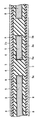
図1は、本発明の実施の形態1におけるプリント配線板の構成を概略的に示す断面図である。また図2は、図1のII−II線に沿う部分の断面を平面視において示す概略断面図である。なお図2のI−I線に沿う断面部分が図1の断面に対応する。また図2においては、説明の便宜上、導電層8の図示は省略されている。
Hereinafter, embodiments of the present invention will be described with reference to the drawings.
(Embodiment 1)
FIG. 1 is a cross-sectional view schematically showing a configuration of a printed wiring board according to Embodiment 1 of the present invention. FIG. 2 is a schematic cross-sectional view showing a cross-section of the portion along the line II-II in FIG. 2 corresponds to the cross section of FIG. 1. In FIG. 2, the
図1を参照して、プリント配線板1は、上下1対の信号回路層4a、4bと、CFRP層5を含むコア(以下、CFRPコアと称する)と、接着部材6と、第1の導電層2bと、被覆層2c、6とを主に有している。
Referring to FIG. 1, printed wiring board 1 includes a pair of upper and lower
上下1対の信号回路層4a、4bの各々は、絶縁基材3と、その絶縁基材3の表面上に形成された信号配線2aとを有している。絶縁基材3は、たとえばガラスクロスにエポキシ樹脂などを含浸したプリプレグを硬化した材質よりなり、CFRP層5との熱膨張率差によって発生する応力を低減するためCFRP層5程度の低熱膨張の材質であることが好ましい。CFRP層5の熱膨張率はたとえば約0ppm/℃である。また絶縁基材3の熱膨張率は一般的には約16ppm/℃であるが、低熱膨張の絶縁基材3の熱膨張率はたとえば約8〜12ppm/℃である。信号配線2aは、たとえば銅よりなっている。
Each of the pair of upper and lower
CFRPコアは、上下1対の信号回路層4a、4bの間に設けられている。このCFRPコアは、CFRP層5と、導電層8とを有している。このCFRP層5は、炭素繊維と樹脂とからなる複合材料であればよく、その複合材料中のカーボン繊維の含有率、構造(一方向材、クロス材)などは特に限定されるものではない。しかしながら、前述したように一方向材からなるプリプレグの成形板は、カーボン繊維と樹脂との界面で剥離し易いため、CFRP層5にはクロス材を用いる方が好ましい。またCFRP層5は、1次貫通穴5aを有している。導電層8は、CFRPコアの1次貫通穴5aの壁面およびCFRP層5の表面の一部と側面とに形成されており、たとえば銅よりなっている。
The CFRP core is provided between a pair of upper and lower
接着部材6は、上下1対の信号回路層4a、4bの各々とCFRPコアとの間に形成され、上下1対の信号回路層4a、4bとCFRPコアとを接着している。この接着部材6は、CFRP層5の1次貫通穴5aの壁面を導電層8を介して覆い、かつ1次貫通穴5a内を通る2次貫通穴1aを有している。接着部材6は、たとえば無機フィラーと樹脂とガラスクロスとから構成され、1〜15W/m・Kの熱伝導率を有することが好ましい。ここで、樹脂は、エポキシ、ビスマレイミド、シアネートエステル、ポリイミドなどに、一部、CTBN(Carboxy-terminated butadiene-acrylonitrile)などゴム成分を混合して弾性率を低下させたものが好ましい。また、無機フィラーの例として、アルミナ、シリカ、マグネシア、窒化アルミニウム、窒化ホウ素、窒化ケイ素などの酸化物や窒化物が挙げられ、その混合物が用いられてもよい。接着部材6にフィラー含有樹脂を用いる理由としては、CFRPコアと2次貫通穴1aの側壁の第1の導電層2bとの間の応力緩和と良熱伝導化のためである。
The
2次貫通穴1aは、1次貫通穴5a内に設けられるので1次貫通穴5aよりも小径であり、上下1対の信号回路層4a、4bの絶縁基材3にも開口されている。
Since the secondary through
第1の導電層2bは、2次貫通穴1aの壁面に形成されており、上下1対の信号回路層4a、4bの各信号配線2a同士を電気的に接続している。この第1の導電層2bはたとえば銅よりなっている。また第1の導電層2bとCFRPコアとは接着部材6によって電気的に絶縁されている。
The first
被覆層2c、6は、CFRPコアの平面視における外周端縁を被覆している。具体的には、CFRPコアの外周端縁5bは被覆層としての接着部材6により被覆されており、CFRPコアの外周端縁5cは被覆層としての第2の導電層2cにより被覆されている。第2の導電層2cはたとえば銅よりなっており、第1の導電層2bと同一の材質よりなっている。
The coating layers 2c and 6 cover the outer peripheral edge in a plan view of the CFRP core. Specifically, the outer
なお導電層2a、2b、2cの表面には、はんだコート(図示せず)が形成されている。このはんだコートは、最終工程でたとえば235℃の温度で5秒間のはんだレベラー処理(つまり、はんだ浴に基板が沈められる処理)が行なわれることにより、第2の導電層2cの表面に形成されるものである。
A solder coat (not shown) is formed on the surfaces of the
図2を参照して、CFRPコアの外周端縁の全周は被覆層2c、6により被覆されている。第2の導電層2cは、CFRPコアの平面視における外周端縁5b、5cのうち接着部材6により被覆されていない外周端縁5cを被覆している。
Referring to FIG. 2, the entire outer peripheral edge of the CFRP core is covered with
次に、本実施の形態のプリント配線板の製造方法について説明する。
図3〜図12は本発明の実施の形態1におけるプリント配線板の製造方法を工程順に示す概略断面図である。また図13〜図17は本発明の実施の形態1におけるプリント配線板の製造方法を工程順に示す図2の断面と同一断面における概略断面図である。
Next, the manufacturing method of the printed wiring board of this Embodiment is demonstrated.
3 to 12 are schematic cross-sectional views showing the method of manufacturing the printed wiring board in Embodiment 1 of the present invention in the order of steps. 13 to 17 are schematic cross-sectional views in the same cross section as the cross section of FIG. 2 showing the method of manufacturing the printed wiring board in the first embodiment of the present invention in the order of steps.
図3を参照して、CFRP層5の両面に、たとえば銅よりなる導電層8が張られたCFRPコアが準備される。
Referring to FIG. 3, a CFRP core in which
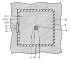
図4および図13を参照して、CFRPコアに1次貫通穴5a、5bが同一の工程で形成される。1次貫通穴5bは、平面視において、たとえばCFRPコアの製品部51と支持部52とを繋ぐ連結部53を残して製品部51の周りを取り囲むように形成される。また1次貫通穴5aは製品部51に形成される。
4 and 13, primary through
なお図13は1次貫通穴5bと連結部53とが1個ずつ形成された状態について示しているが、1次貫通穴5bは複数個に分割されて製品部51の周りを取り囲んでいてもよく、この場合には連結部53も複数個必要となる。また図13は1次貫通穴5aが製品部51に1個形成された状態について示しているが、1次貫通穴5aは製品部51に複数個形成されていてもよい。
Although FIG. 13 shows a state in which one primary through
図5を参照して、CFRPコアに銅めっきが行なわれる。これにより、1次貫通穴5a、5bの各々の壁面が銅めっきよりなる導電層8で被覆され、これによりカーボン粉の脱落が防止される。
Referring to FIG. 5, copper plating is performed on the CFRP core. Thereby, each wall surface of primary through-
図6を参照して、導電層8がパターニングされ、導電層8の不要な部分が除去される。
図7および図14を参照して、たとえば半硬化状態の無機フィラー含有樹脂シートよりなる接着部材6が準備され、真空ラミネートによりCFRPコアの表裏両面に張り合わせられる。このとき、1次貫通穴5a、5bは接着部材6で充填される。
Referring to FIG. 6,
Referring to FIGS. 7 and 14, for example, an
図8を参照して、CFRPコアの両面に接着部材6を介して、たとえば未硬化の絶縁プリプレグよりなる絶縁基材3が貼り付けられる。
Referring to FIG. 8, insulating
図9を参照して、たとえば銅箔よりなる導電層2が絶縁基材3の表面に貼り付けられるとともに、真空プレスを用いて所定の条件で加圧加熱が施される。
Referring to FIG. 9, conductive layer 2 made of, for example, copper foil is attached to the surface of insulating
図10および図15を参照して、2次貫通穴1a、1bが同一の工程で形成される。2次貫通穴1aは1次貫通穴5a内を通るように1次貫通穴5aと同軸上に導電層2、絶縁基材3および接着部材6の各々を貫通して形成される。また2次貫通穴1bは連結部53を跨いで1次貫通穴5bの端部同士を接続するように導電層2、絶縁基材3、接着部材6およびCFRPコアの各々を貫通して形成される。この2次貫通穴1bの壁面においては、CFRP層5が露出する。
Referring to FIGS. 10 and 15, secondary through
図11および図16を参照して、銅めっきが行なわれ、2次貫通穴1aの壁面全面に銅めっきよりなる導電層2bが形成され、2次貫通穴1bの壁面全面に銅めっきよりなる導電層2cが形成される。これによりCFRPコアの表裏両面に形成された導電層2aが導電層2b、2cにより電気的に接続されるとともに、2次貫通穴1bの壁面において露出していたCFRP層5が導電層2cにより被覆される。
Referring to FIGS. 11 and 16, copper plating is performed,
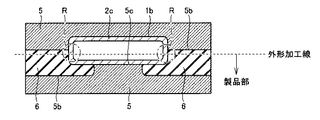
図12および図17を参照して、導電層2aのパターニングが行なわれる。これにより、導電層2aから所定のパターン形状を有する信号配線2aが形成される。この後、ソルダーレジスト塗工、ガスレベラー処理によるはんだコートが行なわれた後に、外形加工が行なわれる。この外形加工は、図中破線の外形加工線で示すように、製品部51と支持部52との間の接着部材6(つまり1次貫通穴5b内の接着部材6)と2次貫通穴1bとの部分をルータ加工で切断しくり抜くことにより行なわれる。これにより、支持部52から製品部51が切り取られて、図1および図2に示す本実施の形態のプリント配線板1が製造される。
Referring to FIGS. 12 and 17, patterning of
本実施の形態のプリント配線板1によれば、図1および図2に示すようにCFRPコアの外周端縁5b、5cが被覆層(第2の導電層2c、接着部材6)により被覆されているため、CFRP層5からのカーボン粉の脱落はなく、ヒートサイクル試験でCFRP層5が剥離することもない。
According to the printed wiring board 1 of the present embodiment, as shown in FIGS. 1 and 2, the outer
またCFRPコアの外周端縁5b、5cの全周を接着部材6で被覆できない理由としては、図1および図2に示す製品のサイズよりも基板製造時のサイズ(ワークサイズ)が大きくなるためである。また製品のサイズよりもワークサイズが大きくなる理由は、ワークの外周部分(製品部51よりも外周の部分)には位置決め穴などの製品には残らない製造過程において必要なものを配置する必要があるためである。
The reason why the entire circumference of the outer
このように製品のサイズよりもワークサイズが大きくなるために、図17に示すように製品部51をその外周の支持部52から切り離す必要がある。ここで、仮に1次貫通穴5bが製品部51の外周全周を途切れることなく連続的に取り囲む場合には、製品部51と支持部52とが完全に分離して、製造途中においてワークから製品部51が抜け落ちてしまい、通常の基板製造設備ではプリント配線板1の製造は困難となる。
Since the workpiece size is larger than the product size in this way, it is necessary to separate the
そこで、製品部51と支持部52とを連結するための連結部53を一部に残す必要がある。しかし、連結部53を残した場合、製品部51を支持部52から切り離す際に、連結部53などのCFRPコアを切断する必要が生じる。このCFRPコアの連結部53などの切断面は接着部材6により被覆されていないため、CFRPコアの外周端縁の全周を接着部材6で被覆することができないのである。
Therefore, it is necessary to leave a
本実施の形態の製造方法においては、図13に示すように1次貫通穴5bを連結部53を残して製品部51を取り囲むように形成することで、製造途中において製品部51がワークから抜け落ちることが防止されている。また図14に示すように、1次貫通穴5b内を接着部材6で埋め込むことにより、CFRPコアの外周端縁5bを接着部材6で被覆することができる。
In the manufacturing method of the present embodiment, as shown in FIG. 13, the primary through
また図15に示すように、1次貫通穴5b内を接着部材6で埋め込んだ状態で連結部53を跨ぐように2次貫通穴1bが形成されるため、この2次貫通穴1bが1次貫通穴5bの端部同士を接続するように形成されても、製品部51がワークから抜け落ちることが防止される。
Further, as shown in FIG. 15, since the secondary through
また図16に示すように、2次貫通穴1aと1bとの双方の壁面に同一の工程で導電層2b、2cが形成されるため、被覆層としての導電層2cを導電層2bと別個の工程で形成する必要がなく、工程を簡略化することができる。また2次貫通穴1bの壁面に被覆層としての導電層2cが形成されるため、2次貫通穴1bの壁面にて露出していたCFRP層5の外周端縁5cを導電層2cで被覆することができる。これにより、CFRP層5からのカーボン粉の脱落、ヒートサイクル試験におけるCFRP層5の剥離を防止することができる。
Further, as shown in FIG. 16, since the
また図17に示す工程における上記のガスレベラー処理によるはんだコート前に切り穴を形成することで、導電層2cの露出を防ぐことが可能である。以下、そのことを説明する。
Moreover, it is possible to prevent the
図18は、図17の領域Pを拡大して示す拡大図である。図18を参照して、ガスレベラー処理によるはんだコートが施されると、導電層2a、2b、2cの表面にはんだがコーティングされる。このため、このはんだコート直後の状態においては、導電層2a、2b、2cの表面は露出していない。しかし、この後に、図中破線で示す外形加工線に沿って切断すると、図19に示すように導電層2cの切断面において銅が外部に露出する。
FIG. 18 is an enlarged view showing a region P in FIG. 17 in an enlarged manner. Referring to FIG. 18, when the solder coating is performed by the gas leveler process, the surface of
一方、図18に示す領域Rに切り穴を形成した後にガスレベラー処理によるはんだコートが施されると、図20に示すように外形加工線に沿って切断した後も、導電層2cの銅が外部に露出することはない。このようにガスレベラー処理によるはんだコート前に切り穴を形成することで、導電層2cの露出を防ぐことが可能となり、導電層2cにはんだによる防錆処理が可能となる。
On the other hand, when solder coating is performed by gas leveler processing after forming a cut hole in the region R shown in FIG. 18, the copper of the
またプリント配線板1の側面の補強と放熱性をさらに向上させるために、銅めっきにより表裏パターンが接続されるとともに、その表裏パターンを短絡するためのスルーホールが設けられてもよい。以下、その構成について説明する。 Further, in order to further improve the side surface reinforcement and heat dissipation of the printed wiring board 1, the front and back patterns may be connected by copper plating, and through holes for short-circuiting the front and back patterns may be provided. Hereinafter, the configuration will be described.
図23は、本発明の実施の形態1におけるプリント配線板の構成を概略的に示す斜視図である。図24は図23のXXIV−XXIV線に沿う概略断面図である。 FIG. 23 is a perspective view schematically showing the configuration of the printed wiring board according to Embodiment 1 of the present invention. 24 is a schematic sectional view taken along line XXIV-XXIV in FIG.
図23および図24を参照して、プリント配線板1の外周端縁付近には、CFRPコア5の表面側には接着部材6および絶縁基板3を介して表面側導電パターン2a1が形成されており、CFRPコア5の裏面側には接着部材6および絶縁基板3を介して裏面側導電パターン2a2が形成されている。これらの表面側導電パターン2a1と裏面側導電パターン2a2との双方は、たとえば銅めっきにより形成された導電材料よりなっている。
Referring to FIGS. 23 and 24, surface side
CFRPコア5の外周端縁5cは被覆層としての第2の導電層2cにより被覆されており、その第2の導電層2cによって表面側導電パターン2a1と裏面側導電パターン2a2とが電気的に接続されている。この第2の導電層2cは、たとえば銅めっきにより形成された導電材料よりなっている。第2の導電層2cはCFRPコア5に接しており、CFRPコア5と電気的に短絡している。
The outer
また表面側導電パターン2a1、裏面側導電パターン2a2、絶縁基板3、CFRPコア5、接着部材6などを貫通する短絡スルーホール1cが形成されている。この短絡スルーホール1cの壁面には、CFRPコア5の露出面を覆うように第3の導電層2dが形成されている。第3の導電層2dは、たとえば銅めっきにより形成された導電材料よりなっている。第3の導電層2dはCFRPコア5に接しており、CFRPコア5と電気的に短絡している。
Further, a short-circuit through
このようにCFRPコア5に接するように第2の導電層2cおよび第3の導電層2dが形成されており、さらに第2の導電層2cおよび第3の導電層2dの各々が表面側導電パターン2a1および裏面側導電パターン2a2の双方に接しているため、プリント配線板1の側面の補強と放熱性をさらに向上させることができる。
Thus, the second
なお図24に示すように、導電層2a〜2d、2a1および2a2の各々の表面ははんだコートされており、各表面にはんだ31が形成されている。また図24において図1の要素と対応する要素には図1に示す符号と同一の符号を付している。
Incidentally, as shown in FIG. 24, the
また図25に示すように上記スルーホール1cを設けたことにより、そのスルーホール1cにねじ42を差し込むことによりプリント配線板1を筐体41に取り付けることができる。これにより、表面側導電パターン2a1と裏面側導電パターン2a2とのいずれかをはんだ31を介して筐体41に接続させることができるため、プリント配線板1から筐体41への放熱性を高めることが可能となる。
Further, by providing the through
またサイズ的な問題でCFRPコア5の外周端縁を第2の導電層2cまたは接着部材6により被覆できない箇所が生じる場合には、図26に示すように、その箇所においてCFRPコア5の外周端縁が樹脂層32により被覆されてもよい。樹脂層32はCFRPコア5の露出部分だけを被覆すればよいが、製造上、その部分だけに塗るのは困難であるため、プリント配線板1の表裏面全体にわたって塗られている。
Further, when there is a portion where the outer peripheral edge of the
この樹脂層32は、たとえばエポキシ樹脂であり、プリント配線板1の製造方法の最終工程で被覆される。また樹脂層32の材質は、エポキシ樹脂に限定されず、接着性、耐熱性などが必要なことから基板材料に用いられている熱硬化系の樹脂が好ましく、たとえばポリイミド樹脂、ビスマレイミドトリアジン樹脂、ポリフェニレンオキサイド樹脂、ポリフェニレンエーテル樹脂などであってもよい。
This
このようにサイズ的な問題で第2の導電層2cおよび接着部材6により被覆できないCFRPコア5の外周端縁を樹脂層32により被覆できるため、CFRPコア5からのカーボン粉の脱落を防止することができる。
Thus, since the outer peripheral edge of the
なお図26は図23のXXVI−XXVI線に沿う概略断面図であり、図26において図1の要素と対応する要素には図1に示す符号と同一の符号を付している。 26 is a schematic sectional view taken along line XXVI-XXVI in FIG. 23. In FIG. 26, elements corresponding to those in FIG. 1 are denoted by the same reference numerals as those in FIG.
(実施の形態2)
実施の形態1では、図8に示す積層体10が形成された後、図9に示すようにその積層体の上下に銅箔2aを置いて積層した場合について説明した。これに対して、本実施の形態では、図8に示す積層体10を用いて4層板のプリント配線板が製造される。以下、そのことについて説明する。
(Embodiment 2)
In Embodiment 1, the case where the
図21は、本発明の実施の形態2におけるプリント配線板の製造方法を示す概略断面図である。図21を参照して、図8に示す積層板10が2つ準備される。これら2つの積層板10の中央に、ガラスエポキシプリプレグ14を介して内層信号回路層13が配置され、また2つの積層板10の内層信号回路層13とは反対側にたとえば銅箔よりなる導電層2aが配置される。この配置状態で、たとえば真空プレスを用いた加圧加熱が施される。その後、図10〜図12および図15〜図17に示す実施の形態1と同様の工程を経ることにより図22に示すような4層板が得られる。
FIG. 21 is a schematic cross-sectional view showing the method for manufacturing the printed wiring board according to Embodiment 2 of the present invention. Referring to FIG. 21, two
なお、上記において内層信号回路層13は、絶縁基材12と、その絶縁基材12の表面上に形成された信号配線11とを有している。絶縁基材12は、たとえばガラスクロスにエポキシ樹脂などを含浸したプリプレグを硬化した材質よりなっている。信号配線2aは、たとえば銅よりなっている。
In the above description, the inner
図22を参照して、上記のようにして得られた4層板の構成においては、上下の接着部材6間に、パターニングされた複数層(たとえば2層)の信号配線11が形成されている。これら複数の信号配線11の各々は他の信号配線とガラスエポキシなどの絶縁層21により電気的に絶縁されている。
Referring to FIG. 22, in the configuration of the four-layer board obtained as described above, a plurality of (for example, two-layer) patterned
また本実施の形態の4層板の構成は、図1に示す実施の形態1の構成と同様、被覆層2c、6が、CFRPコアの平面視における外周端縁5b、5cを被覆している。具体的には、CFRPコアの外周端縁5bは被覆層としての接着部材6により被覆されており、CFRPコアの外周端縁5cは被覆層としての第2の導電層2cにより被覆されている。第2の導電層2cはたとえば銅よりなっており、第1の導電層2bと同一の材質よりなっている。
Further, in the configuration of the four-layer plate of the present embodiment, the coating layers 2c and 6 cover the outer
また図22におけるII−II線に沿う断面の構造は、図2の構成をほぼ同じである。つまり、図2を参照して、CFRPコアの外周端縁の全周は被覆層2c、6により被覆されている。第2の導電層2cは、CFRPコアの平面視における外周端縁5b、5cのうち接着部材6により被覆されていない外周端縁5cを被覆している。
Moreover, the structure of the cross section along the II-II line in FIG. 22 is substantially the same as the structure of FIG. That is, referring to FIG. 2, the entire outer periphery of the CFRP core is covered with the coating layers 2 c and 6. The second
なお上記以外の本実施の形態の構成は実施の形態1の構成とほぼ同じであるため、同一の要素については同一の符号を付し、その説明を省略する。 Since the configuration of the present embodiment other than the above is substantially the same as the configuration of the first embodiment, the same elements are denoted by the same reference numerals and the description thereof is omitted.
本実施の形態においても、実施の形態1と同様の作用効果を得ることができる。 Also in the present embodiment, the same operational effects as in the first embodiment can be obtained.
以下に実施例を示し、さらに詳しく説明する。
(実施例1)
まず、熱伝導率が500W/m・Kのカーボン繊維(クロス材)からなるプリプレグ5(CFRP層5)を18μmの厚みの銅箔8と積層したCFRPコア(厚み0.35mm、サイズ340mm×250mm)を準備した(図3参照)。
Hereinafter, examples will be shown and described in more detail.
Example 1
First, a CFRP core (thickness 0.35 mm, size 340 mm × 250 mm) in which a prepreg 5 (CFRP layer 5) made of carbon fiber (cross material) having a thermal conductivity of 500 W / m · K and a
次に、CFRPコアにドリル穴あけを行ない、直径1.5mmの1次貫通穴5aと幅4mmの長穴の1次貫通穴5bとを設けた(図4参照)。このとき、1次貫通穴5a、5bの壁面からは、カーボン粉が発生する。次に、銅めっきを行なった(図5参照)。このようにすることで1次貫通穴5a、5bの双方の壁面に銅めっき8が形成され、この壁面からのカーボン粉の飛散を防止できる。
Next, a drill hole was drilled in the CFRP core to provide a primary through
次に、不要な部分の銅8をパターニングにより除去した(図6参照)。これにより、CFRP層5の表面から銅がなくなり、CFRP層5の表面が露出する。しかし、銅8から露出したCFRP層5の表面においては、CFRP層5を構成するCFRPプリプレグの樹脂が露出しており、CFRPプリプレグの炭素繊維が露出していないため、カーボン粉は発生しない。また、不要な部分の銅8を除去する目的は、応力緩和と軽量化である。CFRP層5の熱膨張率は±2ppm/℃と低く、銅8(熱膨張率16ppm/℃)をCFRP層5の全面に設けると、熱膨張差による応力が発生し、製品のヒートサイクル試験でCFRP層5と銅8との界面で剥離することがある。
Next, unnecessary portions of
次に、離型フィルムが表裏に貼られた半硬化状態の高熱伝導樹脂シート6(厚み120μm)を準備した。この高熱伝導樹脂は、アルミナフィラーとCTBNを混合したエポキシ樹脂からなり、硬化後の特性は、熱伝導率が3W/m・K、弾性率が19GPa、熱膨張率が27ppm/℃であり、通常樹脂に比べて低熱膨張、低弾性の樹脂である。 Next, a semi-cured high thermal conductive resin sheet 6 (thickness 120 μm) in which release films were attached to the front and back sides was prepared. This high thermal conductive resin is made of an epoxy resin in which an alumina filler and CTBN are mixed, and after curing, the thermal conductivity is 3 W / m · K, the elastic modulus is 19 GPa, and the thermal expansion coefficient is 27 ppm / ° C. Compared to resin, it has low thermal expansion and low elasticity.
次に、片面の離型フィルムを剥がし、ステンレス製の平滑板とともに真空ラミネートした(図7参照)。このラミネート後、表面の離型フィルムを剥がした。 Next, the release film on one side was peeled off and vacuum laminated with a stainless steel smooth plate (see FIG. 7). After this lamination, the release film on the surface was peeled off.
これを2回繰り返し、CFRPコアの表裏に240μmずつ、高熱伝導樹脂シート6を張り合わせた。このとき、1次貫通穴5a、5bを、できるだけ高熱伝導樹脂シート6で充填した。真空ラミネートは、150℃で1min真空引きした後、10kg/cm2で2min加圧することにより行なった。
This was repeated twice, and the high thermal
次に、60μmのガラスエポキシプリプレグ3を準備した。プリプレグ3には、通常プリプレグよりも低熱膨張のもので、日立化成工業株式会社製:GEA−679N(LD)、熱膨張率8〜12ppm/℃のものを使用した。
Next, a 60 μm
プリプレグ3を高熱伝導樹脂シート6の表裏両面に、真空ラミネートした(図8参照)。真空ラミネートは、100℃で30s真空引きした後、10kg/cm2で30s加圧することにより行なった。
The
次に18μmの厚みの銅箔2aとともに、真空プレスを用いて昇温速度5℃/min、保持時間190℃/1h、積層圧力30kg/cm2の条件で加圧加熱することで積層板を得た(図9参照)。
Next, together with the
次に、直径1.5mmの1次貫通穴5aと同軸上に、直径0.9mmの2次貫通穴1aを設けた(図10参照)。また、このとき図15に示すように、CFRPコアに設けた長穴5bと重なるように、幅4mmの長穴の貫通穴1bを形成した(図10参照)。また、このとき図24に示すように直径5mmの短絡スルーホール1cを形成した。
Next, a secondary through
次に、銅めっきを行なって、2次貫通穴1aと貫通穴1bと短絡スルーホール1cとの各壁面に銅層2b、2c、2dを形成した(図11、図24参照)。次に、図18に示す領域Rに切り穴として直径3mmの貫通穴を形成した。次に、銅箔2aのパターニングを行なった(図12、図24参照)。このパターニングの際には、銅層2b、2cとつながるように銅箔2aを残した。また図24に示すように短絡スルーホール1cの壁面の銅層2dにより表面側導電パターン2a1と裏面側導電パターン2a2とが短絡するように銅箔2a1、2a2を残した。
Next, copper plating was performed to form
次に、ソルダーレジスト塗工、ガスレベラー処理によるはんだコートをした後、図12および図17に示す外形加工線に沿って外形加工を行なった。このようにして、図1および図2に示すようなプリント配線板1を得た。 Next, after solder coating by solder resist coating and gas leveler treatment, outer shape processing was performed along the outer shape processing lines shown in FIGS. In this way, a printed wiring board 1 as shown in FIGS. 1 and 2 was obtained.
得られたCFRPコア基板について、CFRPコアと導電層2bとの間の絶縁抵抗を調べた。1000Vを印加したときの絶縁抵抗は、放射線照射前後でいずれも5GΩ以上あり、全く問題ないことがわかった。また、ヒートサイクル試験(−65℃/15min⇔125℃/15min、500サイクル)を実施したところ、短絡・断線などはなく、基板側面にも剥離などは見られなかった。さらに、大型セラミック部品(約10mm×約20mm×約4mm)を上記のCFRPコア基板に実装し、ヒートサイクル試験(−30℃/15min⇔100℃/15min、500サイクル)を実施した。その結果、はんだ接続部にクラックは発生しなかった。
With respect to the obtained CFRP core substrate, the insulation resistance between the CFRP core and the
なお図25に示すように短絡スルーホール1cにねじ42を差し込むことによりプリント配線板1を筐体41に取り付けた。これにより、表面側導電パターン2a1と裏面側導電パターン2a2とのいずれかをはんだ31を介して筐体41に接続させた。
In addition, as shown in FIG. 25, the printed wiring board 1 was attached to the housing | casing 41 by inserting the
(実施例2)
実施例1と同様、CFRPコアに1次貫通穴5aを設け、銅めっきを行ない、パターニングを行なった。次に、高熱伝導樹脂、低熱膨張ガラスエポキシを順次、真空ラミネートにより張り合わせ、図8に示すような積層板10を得た。
(Example 2)
As in Example 1, the CFRP core was provided with primary through
次に、低熱膨張ガラスエポキシ両面銅張板(MCL−E−679(LD)、t0.2mm−18/18μm)を準備し、その銅張板の銅のパターニングを行なった。 Next, a low thermal expansion glass epoxy double-sided copper-clad plate (MCL-E-679 (LD), t0.2 mm-18 / 18 μm) was prepared, and copper patterning of the copper-clad plate was performed.
図21に示すように、上記積層板10と、パターニングされた銅層を有する低熱膨張ガラスエポキシ両面銅張板と、18μmの厚みの銅箔2aとを配置し、真空プレスを用いて昇温速度5℃/min、保持時間190℃/1h、積層圧力30kg/cm2で加圧加熱した。その後、実施例1と同様の工程を行ない、図22に示すような積層板を得た。
As shown in FIG. 21, the
得られたCFRPコア基板について、CFRPコアと導電層2bとの間の絶縁抵抗を調べた。1000Vを印加したときの絶縁抵抗は、放射線照射前後でいずれも5GΩ以上あり、全く問題ないことがわかった。また、ヒートサイクル試験(−65℃/15min⇔125℃/15min、500サイクル)を実施したところ、短絡・断線などはなく、基板側面にも剥離などは見られなかった。さらに、大型セラミック部品(約10mm×約20mm×約4mm)を上記CFRPコア基板に実装し、ヒートサイクル試験(−30℃/15min⇔100℃/15min、500サイクル)を実施した。その結果、はんだ接続部にクラックは発生しなかった。
With respect to the obtained CFRP core substrate, the insulation resistance between the CFRP core and the
なおサイズ的な問題で、被覆層2c、6により被覆できなかったCFRPコア5の外周端縁には、最終工程で、図26に示すように樹脂層32を塗布して被覆した。この樹脂層32の被覆は、塗布したい部分以外の部分(配線部の上など)に粘着力の弱いテープを貼着したうえで、シンナーで希釈したミリオンクリヤー(耐薬品用エポキシ樹脂クリアーペイント(関西ペイント(株)製))を塗布したい部分にハケあるいはスプレーで塗工し、100℃の温度で1時間オーブンで乾燥・硬化させることにより行なった。
In addition, as shown in FIG. 26, the outer peripheral edge of the
今回開示された実施の形態および実施例はすべての点で例示であって制限的なものではないと考えられるべきである。本発明の範囲は上記した説明ではなくて特許請求の範囲によって示され、特許請求の範囲と均等の意味および範囲内でのすべての変更が含まれることが意図される。 It should be understood that the embodiments and examples disclosed herein are illustrative and non-restrictive in every respect. The scope of the present invention is defined by the terms of the claims, rather than the description above, and is intended to include any modifications within the scope and meaning equivalent to the terms of the claims.
本発明は、CFRPを含むコアを有するプリント配線板およびその製造方法に特に有利に適用され得る。 The present invention can be particularly advantageously applied to a printed wiring board having a core containing CFRP and a manufacturing method thereof.
1 プリント配線板、1a,1b 2次貫通穴、2a 信号配線、2b,2c,8 導電層、3 絶縁基材、4a 信号回路層、5 CFRP層、5a 1次貫通穴、5b,5c 外周端縁、6 接着部材、10 積層板、11 信号配線、13 内層信号回路層、14 ガラスエポキシプリプレグ、21 絶縁層、31 はんだ、32 樹脂層、41 筐体、42 ねじ、51 製品部、52 支持部、53 連結部。
DESCRIPTION OF SYMBOLS 1 Printed wiring board, 1a, 1b Secondary through hole, 2a Signal wiring, 2b, 2c, 8 Conductive layer, 3 Insulating base material, 4a Signal circuit layer, 5 CFRP layer, 5a Primary through hole, 5b, 5c Outer edge Edge, 6 Adhesive member, 10 Laminate plate, 11 Signal wiring, 13 Inner signal circuit layer, 14 Glass epoxy prepreg, 21 Insulating layer, 31 Solder, 32 Resin layer, 41 Housing, 42 Screw, 51 Product part, 52
Claims (8)
前記1対の信号回路層の間に設けられた1次貫通穴を有する炭素繊維強化プラスチックを含むコアと、
前記1対の信号回路層と前記コアとを接着し、かつ前記コアの前記1次貫通穴の壁面を覆い、かつ前記1次貫通穴内を通る2次貫通穴を有する接着部材と、
前記1対の信号回路層の各々の前記信号配線を前記2次貫通穴を介して電気的に接続するために前記2次貫通穴の壁面に形成された第1の導電層と、
前記コアの平面視における外周端縁を被覆する被覆層とを備え、
前記被覆層は前記接着部材および第2の導電層を含み、
前記コアの平面視における前記外周端縁は前記接着部材により被覆され、かつ前記接着部材によって被覆されていない前記外周端縁が前記第2の導電層により被覆され、
前記コアの表面側および裏面側の各々に前記接着部材を介して形成された表面側導電パターンおよび裏面側導電パターンをさらに備え、
前記第2の導電層は、めっきにより形成された導電材料よりなり、
前記表面側導電パターンおよび前記裏面側導電パターンは、前記第2の導電層によって互いに電気的に接続されている、プリント配線板。 A pair of signal circuit layers each having a signal wiring;
A core comprising a carbon fiber reinforced plastic having a primary through hole provided between the pair of signal circuit layers;
An adhesive member that adheres the pair of signal circuit layers and the core, covers a wall surface of the primary through hole of the core, and has a secondary through hole passing through the primary through hole;
A first conductive layer formed on a wall surface of the secondary through hole to electrically connect the signal wirings of each of the pair of signal circuit layers through the secondary through hole;
A coating layer covering an outer peripheral edge in a plan view of the core ,
The covering layer includes the adhesive member and a second conductive layer,
The outer peripheral edge in plan view of the core is covered with the adhesive member, and the outer peripheral edge not covered with the adhesive member is covered with the second conductive layer,
A front surface side conductive pattern and a back surface side conductive pattern formed through the adhesive member on each of the front surface side and the back surface side of the core,
The second conductive layer is made of a conductive material formed by plating,
The printed wiring board , wherein the front-side conductive pattern and the back-side conductive pattern are electrically connected to each other by the second conductive layer .
前記短絡スルーホールの壁面に形成された第3の導電層をさらに備え、
前記第3の導電層により前記表面側導電パターンと前記裏面側導電パターンとが電気的に接続されている、請求項1に記載のプリント配線板。 A short-circuit through hole penetrating the front surface side conductive pattern, the back surface side conductive pattern, the adhesive member and the core is formed,
Further comprising a third conductive layer formed on the wall surface of the short-circuited through hole;
The printed wiring board according to claim 1 , wherein the surface-side conductive pattern and the back-side conductive pattern are electrically connected by the third conductive layer.
前記コアの平面視における前記外周端縁のうち前記接着部材および前記第2の導電層によって被覆されていない前記外周端部が前記樹脂層により被覆されている、請求項1〜4のいずれかに記載のプリント配線板。 The coating layer includes a resin layer,
The outer peripheral end portion which is not covered by the adhesive member and the second conductive layer of the outer peripheral edge in a plan view of the core is covered by the resin layer, to any one of claims 1 to 4, The printed wiring board as described.
前記コアの両面を覆い、かつ前記第1および第2の1次貫通穴を埋め込むように接着部材を形成する工程と、
前記コアの両面の各々に前記接着部材を介して、それぞれが信号配線を有する1対の信号回路層の各々を接着する工程と、
前記連結部を跨いで前記第1の1次貫通穴の端部同士を接続するように前記接着部材および前記コアを貫通する第1の2次貫通穴を形成するとともに、前記第2の1次貫通穴内を通るように前記接着部材を貫通する第2の2次貫通穴を形成する工程と、
前記第1および第2の2次貫通穴の壁面に前記コアの両面の前記信号配線とつながる導電層をめっきにより被覆する工程と、
前記製品部と前記支持部との間の前記接着部材および前記第1の2次貫通穴の部分を切断することで前記支持部から前記製品部を切り取る工程とを備えた、プリント配線板の製造方法。 A carbon fiber reinforced plastic having a first primary through hole surrounding the product part leaving a connecting part connecting the product part and the support part, and a second primary through hole formed in the product part. Forming a core comprising:
Forming an adhesive member so as to cover both surfaces of the core and embed the first and second primary through holes;
Bonding each of a pair of signal circuit layers each having a signal wiring to each of both surfaces of the core via the adhesive member;
A first secondary through hole penetrating the adhesive member and the core is formed so as to connect ends of the first primary through hole across the coupling portion, and the second primary Forming a second secondary through hole penetrating the adhesive member so as to pass through the through hole;
Covering the wall surfaces of the first and second secondary through holes with a conductive layer connected to the signal wirings on both surfaces of the core by plating ;
Manufacturing the printed wiring board, comprising: cutting the product part from the support part by cutting the adhesive member between the product part and the support part and the first secondary through hole. Method.
Priority Applications (2)
| Application Number | Priority Date | Filing Date | Title |
|---|---|---|---|
| JP2008204309A JP5076196B2 (en) | 2007-10-29 | 2008-08-07 | Printed wiring board and manufacturing method thereof |
| US12/259,624 US8134085B2 (en) | 2007-10-29 | 2008-10-28 | Printed interconnection board having a core including carbon fiber reinforced plastic |
Applications Claiming Priority (3)
| Application Number | Priority Date | Filing Date | Title |
|---|---|---|---|
| JP2007280422 | 2007-10-29 | ||
| JP2007280422 | 2007-10-29 | ||
| JP2008204309A JP5076196B2 (en) | 2007-10-29 | 2008-08-07 | Printed wiring board and manufacturing method thereof |
Publications (2)
| Publication Number | Publication Date |
|---|---|
| JP2009135415A JP2009135415A (en) | 2009-06-18 |
| JP5076196B2 true JP5076196B2 (en) | 2012-11-21 |
Family
ID=40866987
Family Applications (1)
| Application Number | Title | Priority Date | Filing Date |
|---|---|---|---|
| JP2008204309A Expired - Fee Related JP5076196B2 (en) | 2007-10-29 | 2008-08-07 | Printed wiring board and manufacturing method thereof |
Country Status (1)
| Country | Link |
|---|---|
| JP (1) | JP5076196B2 (en) |
Families Citing this family (7)
| Publication number | Priority date | Publication date | Assignee | Title |
|---|---|---|---|---|
| JP5264651B2 (en) * | 2009-08-24 | 2013-08-14 | 三菱電機株式会社 | Method for manufacturing printed wiring board |
| US8935851B2 (en) | 2010-01-13 | 2015-01-20 | Mitsubishi Electric Corporation | Method for manufacturing a circuit board |
| CN102783258B (en) * | 2010-02-26 | 2016-08-03 | 三菱电机株式会社 | The manufacture method of printed substrate and printed substrate |
| KR101631746B1 (en) * | 2013-05-08 | 2016-07-07 | 주식회사 잉크테크 | Method for making printed circuit board and printed circuit board |
| JP6039867B1 (en) * | 2015-03-06 | 2016-12-07 | 京セラ株式会社 | Winding body and substrate sheet |
| DE112016006058T5 (en) * | 2015-12-25 | 2018-09-06 | Taiyo Yuden Co., Ltd. | PCB and camera module |
| DE102021115851A1 (en) * | 2021-06-18 | 2022-12-22 | Rolls-Royce Deutschland Ltd & Co Kg | circuit board |
Family Cites Families (9)
| Publication number | Priority date | Publication date | Assignee | Title |
|---|---|---|---|---|
| JPS63100798A (en) * | 1986-10-17 | 1988-05-02 | 株式会社日立製作所 | Manufacture of multilayer printed board |
| JP2707996B2 (en) * | 1995-02-24 | 1998-02-04 | 日本電気株式会社 | Hybrid integrated circuit device and method of manufacturing the same |
| JP2004311849A (en) * | 2003-04-09 | 2004-11-04 | Ngk Spark Plug Co Ltd | Wiring board and its producing process |
| JP2005108924A (en) * | 2003-09-29 | 2005-04-21 | Ibiden Co Ltd | Multilayer printed wiring board and its manufacturing method |
| JP3988764B2 (en) * | 2004-10-13 | 2007-10-10 | 三菱電機株式会社 | Printed wiring board substrate, printed wiring board, and printed wiring board substrate manufacturing method |
| JP4316483B2 (en) * | 2004-12-08 | 2009-08-19 | ユーアイ電子株式会社 | Printed circuit board manufacturing method and printed circuit board |
| JP4776247B2 (en) * | 2005-02-09 | 2011-09-21 | 富士通株式会社 | Wiring board and manufacturing method thereof |
| JP4591181B2 (en) * | 2005-04-25 | 2010-12-01 | 三菱電機株式会社 | Printed wiring board |
| JP4689375B2 (en) * | 2005-07-07 | 2011-05-25 | 富士通株式会社 | Laminated substrate and electronic device having the laminated substrate |
-
2008
- 2008-08-07 JP JP2008204309A patent/JP5076196B2/en not_active Expired - Fee Related
Also Published As
| Publication number | Publication date |
|---|---|
| JP2009135415A (en) | 2009-06-18 |
Similar Documents
| Publication | Publication Date | Title |
|---|---|---|
| US9313903B2 (en) | Method of manufacturing printed wiring board | |
| JP5076196B2 (en) | Printed wiring board and manufacturing method thereof | |
| US8134085B2 (en) | Printed interconnection board having a core including carbon fiber reinforced plastic | |
| US9756735B2 (en) | Method for manufacturing printed wiring board | |
| WO2001045478A1 (en) | Multilayered printed wiring board and production method therefor | |
| US10477682B2 (en) | Printed wiring board and method for manufacturing the same | |
| JP2004311736A (en) | Method for manufacturing built-up multilayer wiring board incorporating chip comp0nents | |
| KR20090037794A (en) | Circuit board and method of producing the same | |
| JP2009099621A (en) | Method of manufacturing substrate | |
| KR20090037801A (en) | Core substrate and method of producing the same | |
| JP4992342B2 (en) | Method for manufacturing printed wiring board | |
| JP4907216B2 (en) | Printed wiring board and printed wiring board manufacturing method | |
| JP2006286724A (en) | Wiring board and its manufacturing method | |
| KR101099454B1 (en) | A manufacturing method for multilayer flexible printed cirkit board | |
| JP3969477B2 (en) | Multilayer wiring board and manufacturing method thereof | |
| JP4816343B2 (en) | High heat dissipation substrate and manufacturing method thereof | |
| JP4899409B2 (en) | Multilayer printed wiring board and manufacturing method thereof | |
| KR101204083B1 (en) | Active IC chip embedded multilayer flexible printed circuit board and Method of making the same | |
| KR20120028566A (en) | Carrier member and method of manufacturing pcb using the same | |
| KR20210100589A (en) | Method for manufacturing a package substrate for mounting semiconductor devices | |
| JP5264651B2 (en) | Method for manufacturing printed wiring board | |
| US20220248530A1 (en) | Wiring substrate | |
| JPH06244554A (en) | Multilayered wiring substrate and its manufacture | |
| JP4803919B2 (en) | Manufacturing method of multilayer wiring board | |
| JP2004311870A (en) | Multilayer printed circuit board |
Legal Events
| Date | Code | Title | Description |
|---|---|---|---|
| A621 | Written request for application examination |
Free format text: JAPANESE INTERMEDIATE CODE: A621 Effective date: 20100928 |
|
| A977 | Report on retrieval |
Free format text: JAPANESE INTERMEDIATE CODE: A971007 Effective date: 20120208 |
|
| A131 | Notification of reasons for refusal |
Free format text: JAPANESE INTERMEDIATE CODE: A131 Effective date: 20120214 |
|
| A521 | Request for written amendment filed |
Free format text: JAPANESE INTERMEDIATE CODE: A523 Effective date: 20120323 |
|
| TRDD | Decision of grant or rejection written | ||
| A01 | Written decision to grant a patent or to grant a registration (utility model) |
Free format text: JAPANESE INTERMEDIATE CODE: A01 Effective date: 20120731 |
|
| A01 | Written decision to grant a patent or to grant a registration (utility model) |
Free format text: JAPANESE INTERMEDIATE CODE: A01 |
|
| A61 | First payment of annual fees (during grant procedure) |
Free format text: JAPANESE INTERMEDIATE CODE: A61 Effective date: 20120808 |
|
| FPAY | Renewal fee payment (event date is renewal date of database) |
Free format text: PAYMENT UNTIL: 20150907 Year of fee payment: 3 |
|
| R150 | Certificate of patent or registration of utility model |
Ref document number: 5076196 Country of ref document: JP Free format text: JAPANESE INTERMEDIATE CODE: R150 Free format text: JAPANESE INTERMEDIATE CODE: R150 |
|
| R250 | Receipt of annual fees |
Free format text: JAPANESE INTERMEDIATE CODE: R250 |
|
| R250 | Receipt of annual fees |
Free format text: JAPANESE INTERMEDIATE CODE: R250 |
|
| R250 | Receipt of annual fees |
Free format text: JAPANESE INTERMEDIATE CODE: R250 |
|
| R250 | Receipt of annual fees |
Free format text: JAPANESE INTERMEDIATE CODE: R250 |
|
| R250 | Receipt of annual fees |
Free format text: JAPANESE INTERMEDIATE CODE: R250 |
|
| R250 | Receipt of annual fees |
Free format text: JAPANESE INTERMEDIATE CODE: R250 |
|
| R250 | Receipt of annual fees |
Free format text: JAPANESE INTERMEDIATE CODE: R250 |
|
| LAPS | Cancellation because of no payment of annual fees |