JP5060810B2 - 液晶表示装置及びその駆動方法と製造方法 - Google Patents
液晶表示装置及びその駆動方法と製造方法 Download PDFInfo
- Publication number
- JP5060810B2 JP5060810B2 JP2007083428A JP2007083428A JP5060810B2 JP 5060810 B2 JP5060810 B2 JP 5060810B2 JP 2007083428 A JP2007083428 A JP 2007083428A JP 2007083428 A JP2007083428 A JP 2007083428A JP 5060810 B2 JP5060810 B2 JP 5060810B2
- Authority
- JP
- Japan
- Prior art keywords
- light
- liquid crystal
- display device
- sensor
- electrode
- Prior art date
- Legal status (The legal status is an assumption and is not a legal conclusion. Google has not performed a legal analysis and makes no representation as to the accuracy of the status listed.)
- Expired - Fee Related
Links
Images


Classifications
-
- G—PHYSICS
- G02—OPTICS
- G02F—OPTICAL DEVICES OR ARRANGEMENTS FOR THE CONTROL OF LIGHT BY MODIFICATION OF THE OPTICAL PROPERTIES OF THE MEDIA OF THE ELEMENTS INVOLVED THEREIN; NON-LINEAR OPTICS; FREQUENCY-CHANGING OF LIGHT; OPTICAL LOGIC ELEMENTS; OPTICAL ANALOGUE/DIGITAL CONVERTERS
- G02F1/00—Devices or arrangements for the control of the intensity, colour, phase, polarisation or direction of light arriving from an independent light source, e.g. switching, gating or modulating; Non-linear optics
- G02F1/01—Devices or arrangements for the control of the intensity, colour, phase, polarisation or direction of light arriving from an independent light source, e.g. switching, gating or modulating; Non-linear optics for the control of the intensity, phase, polarisation or colour
- G02F1/13—Devices or arrangements for the control of the intensity, colour, phase, polarisation or direction of light arriving from an independent light source, e.g. switching, gating or modulating; Non-linear optics for the control of the intensity, phase, polarisation or colour based on liquid crystals, e.g. single liquid crystal display cells
- G02F1/133—Constructional arrangements; Operation of liquid crystal cells; Circuit arrangements
-
- G—PHYSICS
- G09—EDUCATION; CRYPTOGRAPHY; DISPLAY; ADVERTISING; SEALS
- G09G—ARRANGEMENTS OR CIRCUITS FOR CONTROL OF INDICATING DEVICES USING STATIC MEANS TO PRESENT VARIABLE INFORMATION
- G09G3/00—Control arrangements or circuits, of interest only in connection with visual indicators other than cathode-ray tubes
- G09G3/20—Control arrangements or circuits, of interest only in connection with visual indicators other than cathode-ray tubes for presentation of an assembly of a number of characters, e.g. a page, by composing the assembly by combination of individual elements arranged in a matrix no fixed position being assigned to or needed to be assigned to the individual characters or partial characters
- G09G3/34—Control arrangements or circuits, of interest only in connection with visual indicators other than cathode-ray tubes for presentation of an assembly of a number of characters, e.g. a page, by composing the assembly by combination of individual elements arranged in a matrix no fixed position being assigned to or needed to be assigned to the individual characters or partial characters by control of light from an independent source
- G09G3/3406—Control of illumination source
-
- G—PHYSICS
- G02—OPTICS
- G02F—OPTICAL DEVICES OR ARRANGEMENTS FOR THE CONTROL OF LIGHT BY MODIFICATION OF THE OPTICAL PROPERTIES OF THE MEDIA OF THE ELEMENTS INVOLVED THEREIN; NON-LINEAR OPTICS; FREQUENCY-CHANGING OF LIGHT; OPTICAL LOGIC ELEMENTS; OPTICAL ANALOGUE/DIGITAL CONVERTERS
- G02F1/00—Devices or arrangements for the control of the intensity, colour, phase, polarisation or direction of light arriving from an independent light source, e.g. switching, gating or modulating; Non-linear optics
- G02F1/01—Devices or arrangements for the control of the intensity, colour, phase, polarisation or direction of light arriving from an independent light source, e.g. switching, gating or modulating; Non-linear optics for the control of the intensity, phase, polarisation or colour
- G02F1/13—Devices or arrangements for the control of the intensity, colour, phase, polarisation or direction of light arriving from an independent light source, e.g. switching, gating or modulating; Non-linear optics for the control of the intensity, phase, polarisation or colour based on liquid crystals, e.g. single liquid crystal display cells
- G02F1/133—Constructional arrangements; Operation of liquid crystal cells; Circuit arrangements
- G02F1/13306—Circuit arrangements or driving methods for the control of single liquid crystal cells
- G02F1/13318—Circuits comprising a photodetector
-
- G—PHYSICS
- G02—OPTICS
- G02F—OPTICAL DEVICES OR ARRANGEMENTS FOR THE CONTROL OF LIGHT BY MODIFICATION OF THE OPTICAL PROPERTIES OF THE MEDIA OF THE ELEMENTS INVOLVED THEREIN; NON-LINEAR OPTICS; FREQUENCY-CHANGING OF LIGHT; OPTICAL LOGIC ELEMENTS; OPTICAL ANALOGUE/DIGITAL CONVERTERS
- G02F1/00—Devices or arrangements for the control of the intensity, colour, phase, polarisation or direction of light arriving from an independent light source, e.g. switching, gating or modulating; Non-linear optics
- G02F1/01—Devices or arrangements for the control of the intensity, colour, phase, polarisation or direction of light arriving from an independent light source, e.g. switching, gating or modulating; Non-linear optics for the control of the intensity, phase, polarisation or colour
- G02F1/13—Devices or arrangements for the control of the intensity, colour, phase, polarisation or direction of light arriving from an independent light source, e.g. switching, gating or modulating; Non-linear optics for the control of the intensity, phase, polarisation or colour based on liquid crystals, e.g. single liquid crystal display cells
- G02F1/133—Constructional arrangements; Operation of liquid crystal cells; Circuit arrangements
- G02F1/1333—Constructional arrangements; Manufacturing methods
- G02F1/1335—Structural association of cells with optical devices, e.g. polarisers or reflectors
-
- G—PHYSICS
- G09—EDUCATION; CRYPTOGRAPHY; DISPLAY; ADVERTISING; SEALS
- G09G—ARRANGEMENTS OR CIRCUITS FOR CONTROL OF INDICATING DEVICES USING STATIC MEANS TO PRESENT VARIABLE INFORMATION
- G09G3/00—Control arrangements or circuits, of interest only in connection with visual indicators other than cathode-ray tubes
- G09G3/20—Control arrangements or circuits, of interest only in connection with visual indicators other than cathode-ray tubes for presentation of an assembly of a number of characters, e.g. a page, by composing the assembly by combination of individual elements arranged in a matrix no fixed position being assigned to or needed to be assigned to the individual characters or partial characters
- G09G3/34—Control arrangements or circuits, of interest only in connection with visual indicators other than cathode-ray tubes for presentation of an assembly of a number of characters, e.g. a page, by composing the assembly by combination of individual elements arranged in a matrix no fixed position being assigned to or needed to be assigned to the individual characters or partial characters by control of light from an independent source
- G09G3/36—Control arrangements or circuits, of interest only in connection with visual indicators other than cathode-ray tubes for presentation of an assembly of a number of characters, e.g. a page, by composing the assembly by combination of individual elements arranged in a matrix no fixed position being assigned to or needed to be assigned to the individual characters or partial characters by control of light from an independent source using liquid crystals
- G09G3/3611—Control of matrices with row and column drivers
- G09G3/3648—Control of matrices with row and column drivers using an active matrix
-
- G—PHYSICS
- G02—OPTICS
- G02F—OPTICAL DEVICES OR ARRANGEMENTS FOR THE CONTROL OF LIGHT BY MODIFICATION OF THE OPTICAL PROPERTIES OF THE MEDIA OF THE ELEMENTS INVOLVED THEREIN; NON-LINEAR OPTICS; FREQUENCY-CHANGING OF LIGHT; OPTICAL LOGIC ELEMENTS; OPTICAL ANALOGUE/DIGITAL CONVERTERS
- G02F1/00—Devices or arrangements for the control of the intensity, colour, phase, polarisation or direction of light arriving from an independent light source, e.g. switching, gating or modulating; Non-linear optics
- G02F1/01—Devices or arrangements for the control of the intensity, colour, phase, polarisation or direction of light arriving from an independent light source, e.g. switching, gating or modulating; Non-linear optics for the control of the intensity, phase, polarisation or colour
- G02F1/13—Devices or arrangements for the control of the intensity, colour, phase, polarisation or direction of light arriving from an independent light source, e.g. switching, gating or modulating; Non-linear optics for the control of the intensity, phase, polarisation or colour based on liquid crystals, e.g. single liquid crystal display cells
- G02F1/133—Constructional arrangements; Operation of liquid crystal cells; Circuit arrangements
- G02F1/13306—Circuit arrangements or driving methods for the control of single liquid crystal cells
- G02F1/13312—Circuits comprising photodetectors for purposes other than feedback
-
- G—PHYSICS
- G09—EDUCATION; CRYPTOGRAPHY; DISPLAY; ADVERTISING; SEALS
- G09G—ARRANGEMENTS OR CIRCUITS FOR CONTROL OF INDICATING DEVICES USING STATIC MEANS TO PRESENT VARIABLE INFORMATION
- G09G2320/00—Control of display operating conditions
- G09G2320/02—Improving the quality of display appearance
- G09G2320/0242—Compensation of deficiencies in the appearance of colours
-
- G—PHYSICS
- G09—EDUCATION; CRYPTOGRAPHY; DISPLAY; ADVERTISING; SEALS
- G09G—ARRANGEMENTS OR CIRCUITS FOR CONTROL OF INDICATING DEVICES USING STATIC MEANS TO PRESENT VARIABLE INFORMATION
- G09G2320/00—Control of display operating conditions
- G09G2320/06—Adjustment of display parameters
- G09G2320/0666—Adjustment of display parameters for control of colour parameters, e.g. colour temperature
-
- G—PHYSICS
- G09—EDUCATION; CRYPTOGRAPHY; DISPLAY; ADVERTISING; SEALS
- G09G—ARRANGEMENTS OR CIRCUITS FOR CONTROL OF INDICATING DEVICES USING STATIC MEANS TO PRESENT VARIABLE INFORMATION
- G09G2360/00—Aspects of the architecture of display systems
- G09G2360/14—Detecting light within display terminals, e.g. using a single or a plurality of photosensors
- G09G2360/141—Detecting light within display terminals, e.g. using a single or a plurality of photosensors the light conveying information used for selecting or modulating the light emitting or modulating element
-
- G—PHYSICS
- G09—EDUCATION; CRYPTOGRAPHY; DISPLAY; ADVERTISING; SEALS
- G09G—ARRANGEMENTS OR CIRCUITS FOR CONTROL OF INDICATING DEVICES USING STATIC MEANS TO PRESENT VARIABLE INFORMATION
- G09G2360/00—Aspects of the architecture of display systems
- G09G2360/14—Detecting light within display terminals, e.g. using a single or a plurality of photosensors
- G09G2360/144—Detecting light within display terminals, e.g. using a single or a plurality of photosensors the light being ambient light
-
- G—PHYSICS
- G09—EDUCATION; CRYPTOGRAPHY; DISPLAY; ADVERTISING; SEALS
- G09G—ARRANGEMENTS OR CIRCUITS FOR CONTROL OF INDICATING DEVICES USING STATIC MEANS TO PRESENT VARIABLE INFORMATION
- G09G2360/00—Aspects of the architecture of display systems
- G09G2360/14—Detecting light within display terminals, e.g. using a single or a plurality of photosensors
- G09G2360/145—Detecting light within display terminals, e.g. using a single or a plurality of photosensors the light originating from the display screen
-
- G—PHYSICS
- G09—EDUCATION; CRYPTOGRAPHY; DISPLAY; ADVERTISING; SEALS
- G09G—ARRANGEMENTS OR CIRCUITS FOR CONTROL OF INDICATING DEVICES USING STATIC MEANS TO PRESENT VARIABLE INFORMATION
- G09G2360/00—Aspects of the architecture of display systems
- G09G2360/16—Calculation or use of calculated indices related to luminance levels in display data
-
- H—ELECTRICITY
- H01—ELECTRIC ELEMENTS
- H01L—SEMICONDUCTOR DEVICES NOT COVERED BY CLASS H10
- H01L27/00—Devices consisting of a plurality of semiconductor or other solid-state components formed in or on a common substrate
- H01L27/02—Devices consisting of a plurality of semiconductor or other solid-state components formed in or on a common substrate including semiconductor components specially adapted for rectifying, oscillating, amplifying or switching and having at least one potential-jump barrier or surface barrier; including integrated passive circuit elements with at least one potential-jump barrier or surface barrier
- H01L27/12—Devices consisting of a plurality of semiconductor or other solid-state components formed in or on a common substrate including semiconductor components specially adapted for rectifying, oscillating, amplifying or switching and having at least one potential-jump barrier or surface barrier; including integrated passive circuit elements with at least one potential-jump barrier or surface barrier the substrate being other than a semiconductor body, e.g. an insulating body
- H01L27/1214—Devices consisting of a plurality of semiconductor or other solid-state components formed in or on a common substrate including semiconductor components specially adapted for rectifying, oscillating, amplifying or switching and having at least one potential-jump barrier or surface barrier; including integrated passive circuit elements with at least one potential-jump barrier or surface barrier the substrate being other than a semiconductor body, e.g. an insulating body comprising a plurality of TFTs formed on a non-semiconducting substrate, e.g. driving circuits for AMLCDs
Description
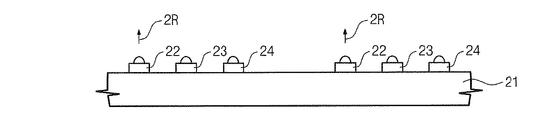
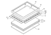
2 第2センサ
10 表示パネル
20 発光ユニット
30 制御部
100 第1基板
200 第2基板
300 液晶層
DA 表示領域
PA 周辺領域
Claims (11)
- 液晶層を利用して映像を表示し、前記液晶層を間に置いて互いに向き合う第1及び第2基板を含む表示パネルと、
前記表示パネルに形成されて外部から入射する入力光を感知する第1センサと、
少なくとも2つの互いに異なる発光源を有し、前記発光源のそれぞれから発生された異なるカラー光による出力光を前記表示パネルに提供する発光ユニットと、
前記表示パネルまたは前記発光ユニットに形成されて、前記出力光を感知する第2センサと、
前記第1センサで感知された入力光に対する分析値を算出し、前記分析値に従って補正された目標値を計算し、前記目標値に対応する前記カラー光が発生するように前記発光源を個別的に制御し、前記第2センサで感知された出力光が前記目標値を満たすか否かを検査する制御部と、
を含み、
前記第1基板は画素領域が定義された表示領域と前記表示領域を囲む周辺領域とを有し、
前記第1センサは前記周辺領域に位置し、
前記第1センサは、
前記第1基板上に前記液晶層と隣接して形成された第1液晶調節電極と、
前記第2基板上に前記液晶層と隣接して形成され、前記第1液晶調節電極と相互作用して前記液晶層に電場を印加する第2液晶調節電極と、
を含むことを特徴とする液晶表示装置。 - 前記分析値は、前記入力光の照度、輝度、波長分布及びカラー温度のうちの少なくともいずれか1つを分析して算出されることを特徴とする請求項1に記載の液晶表示装置。
- 前記目標値は、前記出力光の照度、輝度、波長分布及びカラー温度のうちの少なくともいずれか1つを基準に計算されることを特徴とする請求項2に記載の液晶表示装置。
- 前記制御部は前記分析値に対応する目標値が入力されるデータベースを含むことを特徴とする請求項3に記載の液晶表示装置。
- 前記発光源は赤色光、青色光及び緑色光を発生することを特徴とする請求項1に記載の液晶表示装置。
- 前記出力光は前記赤色光、青色光及び緑色光が組み合わせられた白色光であることを特徴とする請求項5に記載の液晶表示装置。
- 前記出力光は前記赤色光、青色光及び緑色光それぞれによるカラー光であることを特徴とする請求項5に記載の液晶表示装置。
- 前記発光源それぞれは発光ダイオードであることを特徴とする請求項5に記載の液晶表示装置。
- 前記第1センサは、
前記第1基板上に形成された遮光層と、
前記第1基板上に形成された半導体層と、
前記半導体層と前記第1液晶調節電極との間に形成された第1電極と、
前記半導体層と前記第1液晶調節電極との間で前記第1電極と離間するように形成された第2電極と、
をさらに含むことを特徴とする請求項1に記載の液晶表示装置。 - 前記第1センサは前記第2基板と前記第2液晶調節電極との間に形成されたカラーフィルタをさらに含むことを特徴とする請求項1に記載の液晶表示装置。
- 前記表示パネルの上部に結合して前記表示領域の外部をカバーし、前記第1センサと対応する領域に前記入力光が透過するように透過部を有する固定型をさらに含むことを特徴とする請求項1に記載の液晶表示装置。
Applications Claiming Priority (2)
| Application Number | Priority Date | Filing Date | Title |
|---|---|---|---|
| KR10-2006-0084287 | 2006-09-01 | ||
| KR1020060084287A KR101251543B1 (ko) | 2006-09-01 | 2006-09-01 | 액정 표시 장치 및 이의 구동 방법과 제조 방법 |
Publications (3)
| Publication Number | Publication Date |
|---|---|
| JP2008058937A JP2008058937A (ja) | 2008-03-13 |
| JP2008058937A5 JP2008058937A5 (ja) | 2010-04-15 |
| JP5060810B2 true JP5060810B2 (ja) | 2012-10-31 |
Family
ID=39150828
Family Applications (1)
| Application Number | Title | Priority Date | Filing Date |
|---|---|---|---|
| JP2007083428A Expired - Fee Related JP5060810B2 (ja) | 2006-09-01 | 2007-03-28 | 液晶表示装置及びその駆動方法と製造方法 |
Country Status (4)
| Country | Link |
|---|---|
| US (1) | US8013821B2 (ja) |
| JP (1) | JP5060810B2 (ja) |
| KR (1) | KR101251543B1 (ja) |
| CN (1) | CN101135794B (ja) |
Families Citing this family (37)
| Publication number | Priority date | Publication date | Assignee | Title |
|---|---|---|---|---|
| TWI348149B (en) * | 2007-11-12 | 2011-09-01 | Au Optronics Corp | Method for driving field sequential lcd backlight |
| KR101493840B1 (ko) * | 2008-03-14 | 2015-02-17 | 삼성디스플레이 주식회사 | 액정 표시 장치, 표시 시스템, 및 액정 표시 장치를 이용한물체 형상의 인식 방법 |
| KR100871969B1 (ko) * | 2008-04-10 | 2008-12-08 | 주식회사 포트론 | 전광판용 휘도 조절 장치 및 방법 |
| US8125163B2 (en) | 2008-05-21 | 2012-02-28 | Manufacturing Resources International, Inc. | Backlight adjustment system |
| JP2012514956A (ja) | 2009-01-08 | 2012-06-28 | マニュファクチャリング・リソーシズ・インターナショナル・インコーポレーテッド | 装着及びアクセスが可能な部品を備える電子ディスプレイ |
| US9812047B2 (en) | 2010-02-25 | 2017-11-07 | Manufacturing Resources International, Inc. | System and method for remotely monitoring the operating life of electronic displays |
| US8700226B2 (en) * | 2009-02-24 | 2014-04-15 | Manufacturing Resources International, Inc. | Method for driving a cooling fan within an electronic display |
| CA2754371C (en) * | 2009-02-24 | 2017-11-21 | Manufacturing Resources International, Inc. | System and method for controlling the operation parameters of a display in response to current draw |
| TW201102718A (en) * | 2009-07-08 | 2011-01-16 | Dynascan Technology Corp | Decay fast detection method of LED backlight-board liquid crystal display and its display |
| WO2011064870A1 (ja) * | 2009-11-26 | 2011-06-03 | キヤノン株式会社 | 表示パネルの駆動方法及び表示装置 |
| US8508155B2 (en) * | 2010-04-14 | 2013-08-13 | Manufacturing Resources International, Inc. | System and method for calibrating backlight devices |
| US9286020B2 (en) | 2011-02-03 | 2016-03-15 | Manufacturing Resources International, Inc. | System and method for dynamic load sharing between electronic displays |
| CA2849902C (en) | 2011-09-23 | 2019-02-26 | Manufacturing Resources International, Inc. | System and method for environmental adaptation of display characteristics |
| US8928650B2 (en) * | 2012-04-20 | 2015-01-06 | Optoelectronics Technology Co., Ltd | Display panel and 3D display device |
| US9129548B2 (en) * | 2012-11-15 | 2015-09-08 | Apple Inc. | Ambient light sensors with infrared compensation |
| CN103207490B (zh) * | 2013-03-28 | 2015-10-14 | 北京京东方光电科技有限公司 | 一种阵列基板及其制造方法和显示装置 |
| US9530342B2 (en) | 2013-09-10 | 2016-12-27 | Microsoft Technology Licensing, Llc | Ambient light context-aware display |
| WO2015167512A1 (en) * | 2014-04-30 | 2015-11-05 | Hewlett-Packard Development Company, L.P. | Large gamut pixel and subtractive mask for a visual presentation |
| CN105590578A (zh) * | 2014-10-20 | 2016-05-18 | 深圳富泰宏精密工业有限公司 | 自动开启蓝光滤波器护眼系统及方法 |
| US10593255B2 (en) | 2015-05-14 | 2020-03-17 | Manufacturing Resources International, Inc. | Electronic display with environmental adaptation of display characteristics based on location |
| US10321549B2 (en) | 2015-05-14 | 2019-06-11 | Manufacturing Resources International, Inc. | Display brightness control based on location data |
| US10607520B2 (en) | 2015-05-14 | 2020-03-31 | Manufacturing Resources International, Inc. | Method for environmental adaptation of display characteristics based on location |
| JP6639653B2 (ja) | 2015-09-10 | 2020-02-05 | マニュファクチャリング・リソーシズ・インターナショナル・インコーポレーテッド | ディスプレイエラーのシステム検出のためのシステムおよび方法 |
| US10586508B2 (en) | 2016-07-08 | 2020-03-10 | Manufacturing Resources International, Inc. | Controlling display brightness based on image capture device data |
| KR20190029832A (ko) | 2017-09-11 | 2019-03-21 | 삼성디스플레이 주식회사 | 표시장치 |
| US10578658B2 (en) | 2018-05-07 | 2020-03-03 | Manufacturing Resources International, Inc. | System and method for measuring power consumption of an electronic display assembly |
| US10782276B2 (en) | 2018-06-14 | 2020-09-22 | Manufacturing Resources International, Inc. | System and method for detecting gas recirculation or airway occlusion |
| US10908863B2 (en) | 2018-07-12 | 2021-02-02 | Manufacturing Resources International, Inc. | System and method for providing access to co-located operations data for an electronic display |
| CN109272968A (zh) * | 2018-11-21 | 2019-01-25 | 维沃移动通信有限公司 | 一种屏幕均匀性校准方法及终端设备 |
| JP7311538B2 (ja) * | 2019-01-04 | 2023-07-19 | 京東方科技集團股▲ふん▼有限公司 | 表示装置用可撓性表示パネル及び表示装置 |
| WO2020176416A1 (en) | 2019-02-25 | 2020-09-03 | Manufacturing Resources International, Inc. | Monitoring the status of a touchscreen |
| US11402940B2 (en) | 2019-02-25 | 2022-08-02 | Manufacturing Resources International, Inc. | Monitoring the status of a touchscreen |
| CN110459159B (zh) * | 2019-08-15 | 2021-08-31 | 成都辰显光电有限公司 | 一种显示装置及其驱动方法 |
| US11526044B2 (en) | 2020-03-27 | 2022-12-13 | Manufacturing Resources International, Inc. | Display unit with orientation based operation |
| CN115428061A (zh) * | 2020-07-02 | 2022-12-02 | 华为技术有限公司 | 显示装置及驱动显示装置的方法 |
| US11965804B2 (en) | 2021-07-28 | 2024-04-23 | Manufacturing Resources International, Inc. | Display assemblies with differential pressure sensors |
| US11921010B2 (en) | 2021-07-28 | 2024-03-05 | Manufacturing Resources International, Inc. | Display assemblies with differential pressure sensors |
Family Cites Families (17)
| Publication number | Priority date | Publication date | Assignee | Title |
|---|---|---|---|---|
| JP3015400B2 (ja) * | 1990-02-28 | 2000-03-06 | 株式会社東芝 | 液晶表示装置 |
| JP4048627B2 (ja) * | 1998-10-20 | 2008-02-20 | カシオ計算機株式会社 | 表示装置 |
| US6559826B1 (en) * | 1998-11-06 | 2003-05-06 | Silicon Graphics, Inc. | Method for modeling and updating a colorimetric reference profile for a flat panel display |
| JP2001127837A (ja) | 1999-10-29 | 2001-05-11 | Hitachi Ltd | 携帯電話器 |
| JP2002072920A (ja) | 2000-08-25 | 2002-03-12 | Sharp Corp | 表示装置 |
| JP4073272B2 (ja) * | 2002-08-29 | 2008-04-09 | シチズン電子株式会社 | カラー表示装置およびカラー表示装置の白色バランス調整方法 |
| JP4076083B2 (ja) | 2003-04-01 | 2008-04-16 | 株式会社Hdt | Ledの駆動電圧設定装置及びその方法 |
| US7420538B2 (en) * | 2003-12-03 | 2008-09-02 | Sharp Kabushiki Kaisha | Liquid crystal display device and driving device thereof, and method for driving liquid crystal display device |
| TW200620181A (en) * | 2004-12-01 | 2006-06-16 | Chi Lin Technology Co Ltd | Brightness control device and method of intelligent display panel |
| JP4612406B2 (ja) * | 2004-02-09 | 2011-01-12 | 株式会社日立製作所 | 液晶表示装置 |
| JP4628770B2 (ja) * | 2004-02-09 | 2011-02-09 | 株式会社日立製作所 | 照明装置を備えた画像表示装置及び画像表示方法 |
| EP1605342A3 (en) * | 2004-06-10 | 2010-01-20 | Samsung Electronics Co, Ltd | Display device and driving method thereof |
| JP4163156B2 (ja) * | 2004-07-27 | 2008-10-08 | 株式会社半導体エネルギー研究所 | 表示装置 |
| JP4529585B2 (ja) * | 2004-08-18 | 2010-08-25 | ソニー株式会社 | 表示装置及びその制御装置 |
| JP4539492B2 (ja) * | 2004-11-19 | 2010-09-08 | ソニー株式会社 | バックライト装置、バックライト駆動方法及び液晶表示装置 |
| JP4955262B2 (ja) * | 2004-12-07 | 2012-06-20 | サムスン エレクトロニクス カンパニー リミテッド | 液晶表示装置、光感知素子、及びバックライト光源の照度制御装置 |
| KR101097920B1 (ko) * | 2004-12-10 | 2011-12-23 | 삼성전자주식회사 | 광 센서와, 이를 구비한 표시 패널 및 표시 장치 |
-
2006
- 2006-09-01 KR KR1020060084287A patent/KR101251543B1/ko not_active IP Right Cessation
-
2007
- 2007-03-28 JP JP2007083428A patent/JP5060810B2/ja not_active Expired - Fee Related
- 2007-08-28 US US11/846,438 patent/US8013821B2/en not_active Expired - Fee Related
- 2007-09-03 CN CN2007101488084A patent/CN101135794B/zh not_active Expired - Fee Related
Also Published As
| Publication number | Publication date |
|---|---|
| US8013821B2 (en) | 2011-09-06 |
| KR20080020859A (ko) | 2008-03-06 |
| CN101135794B (zh) | 2013-06-26 |
| KR101251543B1 (ko) | 2013-04-08 |
| JP2008058937A (ja) | 2008-03-13 |
| US20080055297A1 (en) | 2008-03-06 |
| CN101135794A (zh) | 2008-03-05 |
Similar Documents
| Publication | Publication Date | Title |
|---|---|---|
| JP5060810B2 (ja) | 液晶表示装置及びその駆動方法と製造方法 | |
| JP4753661B2 (ja) | 表示装置 | |
| KR101189268B1 (ko) | 액정 표시 장치용 박막 표시판 및 구동 장치와 이를 포함하는 액정 표시 장치 | |
| US8432510B2 (en) | Liquid crystal display device and light detector having first and second TFT ambient light photo-sensors alternatively arranged on the same row | |
| JP4514674B2 (ja) | 表示装置、表示パネル用基板および表示パネル用基板の製造方法 | |
| US10796628B2 (en) | Luminance compensation method of light-emitting device | |
| TW202011097A (zh) | 顯示面板 | |
| US20190101779A1 (en) | Display screen, electronic device, and light intensity detection method | |
| KR20110121621A (ko) | 디스플레이 디바이스에서의 광감지 | |
| US20060118697A1 (en) | Liquid crystal display apparatus, light-sensing element and apparatus for controlling luminance of a light source | |
| KR20090032812A (ko) | 디스플레이장치 및 그 제어방법 | |
| JP2006108095A (ja) | 照明装置および調整方法 | |
| JP2006278368A (ja) | 光源装置および表示装置 | |
| JP2008170509A (ja) | 調光機能を備えた画像表示装置 | |
| US20070069632A1 (en) | Electroluminescent device and pixel device | |
| US20070171669A1 (en) | Backlight assembly and liquid crystal display device having the same | |
| JP2007304520A (ja) | カラー液晶表示装置 | |
| TW201403056A (zh) | 顯示面板之製造方法、其檢查裝置及檢查方法 | |
| JP4552719B2 (ja) | 電気光学装置及び電子機器 | |
| JP2002278506A (ja) | 発光輝度調整手段を備えた発光装置及び該発光装置を用いた表示装置 | |
| JP4591244B2 (ja) | 表示装置 | |
| CN110176484A (zh) | 一种显示装置 | |
| JP4622615B2 (ja) | 電気光学装置及び電子機器 | |
| JP2007018845A (ja) | 照明装置、照明装置を備えた電気光学装置、及びそのような電気光学装置を用いた光学特性の調整方法、並びに電子機器 | |
| CN113433730A (zh) | 液晶显示面板及显示装置 |
Legal Events
| Date | Code | Title | Description |
|---|---|---|---|
| A521 | Written amendment |
Free format text: JAPANESE INTERMEDIATE CODE: A523 Effective date: 20100226 |
|
| A621 | Written request for application examination |
Free format text: JAPANESE INTERMEDIATE CODE: A621 Effective date: 20100226 |
|
| A521 | Written amendment |
Free format text: JAPANESE INTERMEDIATE CODE: A523 Effective date: 20110131 |
|
| A977 | Report on retrieval |
Free format text: JAPANESE INTERMEDIATE CODE: A971007 Effective date: 20120220 |
|
| A131 | Notification of reasons for refusal |
Free format text: JAPANESE INTERMEDIATE CODE: A131 Effective date: 20120228 |
|
| A521 | Written amendment |
Free format text: JAPANESE INTERMEDIATE CODE: A523 Effective date: 20120509 |
|
| RD02 | Notification of acceptance of power of attorney |
Free format text: JAPANESE INTERMEDIATE CODE: A7422 Effective date: 20120509 |
|
| TRDD | Decision of grant or rejection written | ||
| A01 | Written decision to grant a patent or to grant a registration (utility model) |
Free format text: JAPANESE INTERMEDIATE CODE: A01 Effective date: 20120731 |
|
| A01 | Written decision to grant a patent or to grant a registration (utility model) |
Free format text: JAPANESE INTERMEDIATE CODE: A01 |
|
| A61 | First payment of annual fees (during grant procedure) |
Free format text: JAPANESE INTERMEDIATE CODE: A61 Effective date: 20120806 |
|
| FPAY | Renewal fee payment (event date is renewal date of database) |
Free format text: PAYMENT UNTIL: 20150810 Year of fee payment: 3 |
|
| R150 | Certificate of patent or registration of utility model |
Free format text: JAPANESE INTERMEDIATE CODE: R150 |
|
| FPAY | Renewal fee payment (event date is renewal date of database) |
Free format text: PAYMENT UNTIL: 20150810 Year of fee payment: 3 |
|
| S111 | Request for change of ownership or part of ownership |
Free format text: JAPANESE INTERMEDIATE CODE: R313111 |
|
| S631 | Written request for registration of reclamation of domicile |
Free format text: JAPANESE INTERMEDIATE CODE: R313631 |
|
| FPAY | Renewal fee payment (event date is renewal date of database) |
Free format text: PAYMENT UNTIL: 20150810 Year of fee payment: 3 |
|
| R371 | Transfer withdrawn |
Free format text: JAPANESE INTERMEDIATE CODE: R371 |
|
| S631 | Written request for registration of reclamation of domicile |
Free format text: JAPANESE INTERMEDIATE CODE: R313631 |
|
| R350 | Written notification of registration of transfer |
Free format text: JAPANESE INTERMEDIATE CODE: R350 |
|
| S111 | Request for change of ownership or part of ownership |
Free format text: JAPANESE INTERMEDIATE CODE: R313111 |
|
| R350 | Written notification of registration of transfer |
Free format text: JAPANESE INTERMEDIATE CODE: R350 |
|
| R250 | Receipt of annual fees |
Free format text: JAPANESE INTERMEDIATE CODE: R250 |
|
| R250 | Receipt of annual fees |
Free format text: JAPANESE INTERMEDIATE CODE: R250 |
|
| R250 | Receipt of annual fees |
Free format text: JAPANESE INTERMEDIATE CODE: R250 |
|
| LAPS | Cancellation because of no payment of annual fees |