JP5057639B2 - フォトニックバンドギャップファイバの製造方法 - Google Patents
フォトニックバンドギャップファイバの製造方法 Download PDFInfo
- Publication number
- JP5057639B2 JP5057639B2 JP2003510400A JP2003510400A JP5057639B2 JP 5057639 B2 JP5057639 B2 JP 5057639B2 JP 2003510400 A JP2003510400 A JP 2003510400A JP 2003510400 A JP2003510400 A JP 2003510400A JP 5057639 B2 JP5057639 B2 JP 5057639B2
- Authority
- JP
- Japan
- Prior art keywords
- preform
- etchant
- etching
- photonic
- fiber
- Prior art date
- Legal status (The legal status is an assumption and is not a legal conclusion. Google has not performed a legal analysis and makes no representation as to the accuracy of the status listed.)
- Expired - Fee Related
Links
Images


Classifications
-
- C—CHEMISTRY; METALLURGY
- C03—GLASS; MINERAL OR SLAG WOOL
- C03B—MANUFACTURE, SHAPING, OR SUPPLEMENTARY PROCESSES
- C03B37/00—Manufacture or treatment of flakes, fibres, or filaments from softened glass, minerals, or slags
- C03B37/01—Manufacture of glass fibres or filaments
- C03B37/012—Manufacture of preforms for drawing fibres or filaments
- C03B37/01205—Manufacture of preforms for drawing fibres or filaments starting from tubes, rods, fibres or filaments
- C03B37/01225—Means for changing or stabilising the shape, e.g. diameter, of tubes or rods in general, e.g. collapsing
- C03B37/01228—Removal of preform material
- C03B37/01231—Removal of preform material to form a longitudinal hole, e.g. by drilling
-
- G—PHYSICS
- G02—OPTICS
- G02B—OPTICAL ELEMENTS, SYSTEMS OR APPARATUS
- G02B6/00—Light guides; Structural details of arrangements comprising light guides and other optical elements, e.g. couplings
-
- C—CHEMISTRY; METALLURGY
- C03—GLASS; MINERAL OR SLAG WOOL
- C03B—MANUFACTURE, SHAPING, OR SUPPLEMENTARY PROCESSES
- C03B2203/00—Fibre product details, e.g. structure, shape
- C03B2203/10—Internal structure or shape details
- C03B2203/14—Non-solid, i.e. hollow products, e.g. hollow clad or with core-clad interface
-
- C—CHEMISTRY; METALLURGY
- C03—GLASS; MINERAL OR SLAG WOOL
- C03B—MANUFACTURE, SHAPING, OR SUPPLEMENTARY PROCESSES
- C03B2203/00—Fibre product details, e.g. structure, shape
- C03B2203/42—Photonic crystal fibres, e.g. fibres using the photonic bandgap PBG effect, microstructured or holey optical fibres
Description

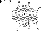
dは内部通路の直径であり、
Λは隣接する通路の中心間の距離、すなわちピッチである。
Joannopoulus et al., "Photonic Crystals: putting a new twist on light", Nature vol.386, March 13, 1997, pp.143-149 Birks et al., "Full 2-D photonic band gaps in silica/air structures", Electronic Letters, Vol.31(22), October 26, 1995, pp.1941-1943 R.F.Cregan, Single-Mode Photonic Band Gap Guidance of Light in Air, SCIENCE, vol.285, pp.1537-39(1999)
12 プリフォーム
18 エッチング剤
20 フラッシング剤
28 貯留槽
32 循環器
42,48 弁
52 支持体
Claims (5)
- フォトニックバンドギャップファイバを製造する方法であって、
複数の長手方向の通路を有するフォトニック結晶プリフォームを製造し、
前記複数の長手方向の通路から材料を除去することにより、所定の量だけ前記複数の長手方向の通路を拡大して、前記フォトニック結晶プリフォームの空隙率が0.82またはそれ以上の制御された値になるように、前記フォトニック結晶プリフォームをエッチングし、
エッチングされた前記フォトニック結晶プリフォームからフォトニックバンドギャップファイバを製造する、
各工程を有してなることを特徴とする方法。 - 前記フォトニック結晶プリフォームをエッチングする工程が、
エッチング剤を前記複数の長手方向の通路に通して流動させる工程を含むことを特徴とする請求項1記載の方法。 - 前記フォトニックバンドギャップファイバを製造する工程が、
前記エッチングされたフォトニック結晶プリフォームをフォトニックバンドギャップファイバに線引きする工程を含むことを特徴とする請求項1記載の方法。 - 前記フォトニック結晶プリフォームを製造する工程が、
複数の中空コアガラス棒材を所定の配列に配置する工程を含むことを特徴とする請求項1記載の方法。 - 請求項1乃至4のいずれか1項に記載の方法により製造されたフォトニックバンドギャップファイバを有してなる光導波路ファイバ。
Applications Claiming Priority (1)
| Application Number | Priority Date | Filing Date | Title |
|---|---|---|---|
| PCT/US2001/021503 WO2003004425A1 (en) | 2000-04-28 | 2001-07-06 | Method of making photonic band gap fibers |
Related Child Applications (1)
| Application Number | Title | Priority Date | Filing Date |
|---|---|---|---|
| JP2012012981A Division JP5705758B2 (ja) | 2012-01-25 | 2012-01-25 | フォトニックバンドギャップファイバの製造方法 |
Publications (3)
| Publication Number | Publication Date |
|---|---|
| JP2004533398A JP2004533398A (ja) | 2004-11-04 |
| JP2004533398A5 JP2004533398A5 (ja) | 2008-08-21 |
| JP5057639B2 true JP5057639B2 (ja) | 2012-10-24 |
Family
ID=32092073
Family Applications (1)
| Application Number | Title | Priority Date | Filing Date |
|---|---|---|---|
| JP2003510400A Expired - Fee Related JP5057639B2 (ja) | 2001-07-06 | 2001-07-06 | フォトニックバンドギャップファイバの製造方法 |
Country Status (3)
| Country | Link |
|---|---|
| EP (1) | EP1414763B1 (ja) |
| JP (1) | JP5057639B2 (ja) |
| KR (1) | KR100798554B1 (ja) |
Cited By (1)
| Publication number | Priority date | Publication date | Assignee | Title |
|---|---|---|---|---|
| JP2012140323A (ja) * | 2012-01-25 | 2012-07-26 | Corning Inc | フォトニックバンドギャップファイバの製造方法 |
Families Citing this family (4)
| Publication number | Priority date | Publication date | Assignee | Title |
|---|---|---|---|---|
| EP1664852B1 (en) * | 2003-09-12 | 2016-12-14 | The Board of Trustees of The Leland Stanford Junior University | Method for configuring air-core photonic-bandgap fibers free of surface modes |
| US7228041B2 (en) | 2004-05-08 | 2007-06-05 | The Board Of Trustees Of The Leland Stanford Junior University | Photonic-bandgap fiber with a core ring |
| WO2005031930A1 (ja) | 2003-09-26 | 2005-04-07 | The Furukawa Electric Co., Ltd. | 半導体レーザ装置 |
| US7346250B1 (en) * | 2007-03-30 | 2008-03-18 | Corning Incorporated | Preferential etching method of forming microstructure for an optical waveguide |
Family Cites Families (11)
| Publication number | Priority date | Publication date | Assignee | Title |
|---|---|---|---|---|
| US4294271A (en) | 1979-11-30 | 1981-10-13 | Dexon, Inc. | Apparatus for removing deposited matter from a diffusion tube |
| US5372653A (en) | 1993-05-28 | 1994-12-13 | Courtaulds Fibres (Holdings) Limited | Cleaning of filters |
| IT1267418B1 (it) | 1994-03-16 | 1997-02-05 | Cselt Centro Studi Lab Telecom | Procedimento per la realizzazione di fibre ottiche monomodo in vetro fluorurato. |
| US5897679A (en) * | 1997-08-27 | 1999-04-27 | Lucent Technologies Inc. | Dimensional control in the manufacture of optical fiber ferrule connectors by etching |
| EP1177092A4 (en) * | 1999-02-18 | 2004-11-17 | Corning Inc | HONEYCOMB SILICA GLASS STRUCTURE MADE BY EXTRUSION OF SILICA SOOT |
| AU2001241172A1 (en) * | 2000-05-01 | 2001-11-12 | Sumitomo Electric Industries, Ltd. | Optical fiber and method for manufacturing the same |
| JP3556908B2 (ja) * | 2001-01-15 | 2004-08-25 | 三菱電線工業株式会社 | フォトニッククリスタルファイバの製造方法 |
| JP4759816B2 (ja) * | 2001-02-21 | 2011-08-31 | 住友電気工業株式会社 | 光ファイバの製造方法 |
| GB2394712B (en) * | 2001-03-09 | 2005-10-26 | Crystal Fibre As | Fabrication of microstructured fibres |
| JP2002293562A (ja) * | 2001-03-29 | 2002-10-09 | Sumitomo Electric Ind Ltd | 光ファイバの製造方法 |
| JP2002321935A (ja) * | 2001-04-20 | 2002-11-08 | Sumitomo Electric Ind Ltd | 光ファイバの製造方法及び光ファイバ |
-
2001
- 2001-07-06 JP JP2003510400A patent/JP5057639B2/ja not_active Expired - Fee Related
- 2001-07-06 EP EP01958883A patent/EP1414763B1/en not_active Expired - Lifetime
- 2001-07-06 KR KR1020047000179A patent/KR100798554B1/ko not_active IP Right Cessation
Cited By (1)
| Publication number | Priority date | Publication date | Assignee | Title |
|---|---|---|---|---|
| JP2012140323A (ja) * | 2012-01-25 | 2012-07-26 | Corning Inc | フォトニックバンドギャップファイバの製造方法 |
Also Published As
| Publication number | Publication date |
|---|---|
| KR100798554B1 (ko) | 2008-01-28 |
| EP1414763B1 (en) | 2012-11-28 |
| EP1414763A1 (en) | 2004-05-06 |
| JP2004533398A (ja) | 2004-11-04 |
| EP1414763A4 (en) | 2006-07-19 |
| KR20040014658A (ko) | 2004-02-14 |
Similar Documents
| Publication | Publication Date | Title |
|---|---|---|
| US6444133B1 (en) | Method of making photonic band gap fibers | |
| US7346250B1 (en) | Preferential etching method of forming microstructure for an optical waveguide | |
| JP6831370B2 (ja) | 中空コア・ファイバおよびその製造方法 | |
| KR100637542B1 (ko) | 광자결정 광섬유의 제조방법 | |
| US9971087B2 (en) | High-birefringence hollow-core fibers and techniques for making same | |
| US20040022508A1 (en) | Holey optical fibres | |
| JP7332706B2 (ja) | フォトニック結晶ファイバのプリフォーム、その製造方法及びフォトニック結晶ファイバ | |
| US20090067793A1 (en) | Multiple Core Microstructured Optical Fibre | |
| AU3810699A (en) | Microstructured optical fibres | |
| WO2006119334A9 (en) | Microstructured optical fibers and manufacturing methods thereof | |
| US20100008634A1 (en) | Optical fiber article for handling higher power and method of fabricating or using | |
| KR20050081236A (ko) | 다공 광섬유 및 그 제조방법 | |
| JP4158391B2 (ja) | 光ファイバおよびその製造方法 | |
| JP5057639B2 (ja) | フォトニックバンドギャップファイバの製造方法 | |
| WO2002075392A2 (en) | Optimized defects in phonotic band-gap waveguides | |
| JP5705758B2 (ja) | フォトニックバンドギャップファイバの製造方法 | |
| GB2457946A (en) | Method of manufacturing a photonic bandgap fibre | |
| JP5539594B2 (ja) | ファイバ及びファイバの製造方法 | |
| EP1309890B1 (en) | Holey optical fibres, preforms and manufacturing methods | |
| CN113853360B (zh) | 用于制造空芯光纤的方法和设备 | |
| Jasion et al. | Virtual draw of tubular hollow-core fibers | |
| JP2002029769A (ja) | 光ファイバの製造方法 | |
| WO2006068709A1 (en) | Hole-assisted fiber and its method of making | |
| WO2002010817A1 (en) | An optical waveguide | |
| JP2007033547A (ja) | フォトニックバンドギャップファイバとその製造方法 |
Legal Events
| Date | Code | Title | Description |
|---|---|---|---|
| A521 | Written amendment |
Free format text: JAPANESE INTERMEDIATE CODE: A821 Effective date: 20040705 |
|
| A521 | Written amendment |
Free format text: JAPANESE INTERMEDIATE CODE: A523 Effective date: 20080703 |
|
| A621 | Written request for application examination |
Free format text: JAPANESE INTERMEDIATE CODE: A621 Effective date: 20080703 |
|
| A131 | Notification of reasons for refusal |
Free format text: JAPANESE INTERMEDIATE CODE: A131 Effective date: 20111025 |
|
| A521 | Written amendment |
Free format text: JAPANESE INTERMEDIATE CODE: A523 Effective date: 20120125 |
|
| TRDD | Decision of grant or rejection written | ||
| A01 | Written decision to grant a patent or to grant a registration (utility model) |
Free format text: JAPANESE INTERMEDIATE CODE: A01 Effective date: 20120703 |
|
| A01 | Written decision to grant a patent or to grant a registration (utility model) |
Free format text: JAPANESE INTERMEDIATE CODE: A01 |
|
| A61 | First payment of annual fees (during grant procedure) |
Free format text: JAPANESE INTERMEDIATE CODE: A61 Effective date: 20120731 |
|
| FPAY | Renewal fee payment (event date is renewal date of database) |
Free format text: PAYMENT UNTIL: 20150810 Year of fee payment: 3 |
|
| R150 | Certificate of patent or registration of utility model |
Free format text: JAPANESE INTERMEDIATE CODE: R150 |
|
| R250 | Receipt of annual fees |
Free format text: JAPANESE INTERMEDIATE CODE: R250 |
|
| LAPS | Cancellation because of no payment of annual fees |