JP5037814B2 - Memory control device and memory control method - Google Patents
Memory control device and memory control method Download PDFInfo
- Publication number
- JP5037814B2 JP5037814B2 JP2005346892A JP2005346892A JP5037814B2 JP 5037814 B2 JP5037814 B2 JP 5037814B2 JP 2005346892 A JP2005346892 A JP 2005346892A JP 2005346892 A JP2005346892 A JP 2005346892A JP 5037814 B2 JP5037814 B2 JP 5037814B2
- Authority
- JP
- Japan
- Prior art keywords
- data
- transfer
- processing means
- transferred
- memory
- Prior art date
- Legal status (The legal status is an assumption and is not a legal conclusion. Google has not performed a legal analysis and makes no representation as to the accuracy of the status listed.)
- Expired - Fee Related
Links
Images

Description
本発明は、メモリ制御装置及びメモリ制御方法に関し、詳しくは共通使用されるメモリに係るデータ転送技術に関する。 The present invention relates to a memory control device and a memory control method, and more particularly to a data transfer technique related to a commonly used memory.
従来より、各種処理部、メモリ、及び入出力部等が各々バスによって接続されるシステムにおいて、システム全体のコストを抑えるために、各処理部が1つのメモリを共有して使用する方法が提案されている。動画像信号や音声信号などを扱うシステムでは、一定時間に所定の処理を行う処理部が複数存在して、それらが同時に動作しているため、各処理部がメモリとの間で行うデータ転送も一定時間内に終了しなければならない。 Conventionally, in a system in which various processing units, memories, input / output units, and the like are connected by buses, a method has been proposed in which each processing unit shares and uses one memory in order to reduce the overall cost of the system. ing. In a system that handles moving image signals, audio signals, etc., there are a plurality of processing units that perform predetermined processing at a fixed time, and they operate simultaneously, so that each processing unit also performs data transfer with the memory. Must finish within a certain time.
一般に、そのようなシステムのメモリ制御部は、1つの処理部がメモリを長時間占有することを防止するため、各処理部からのメモリアクセス要求を優先度に従って調停するアービタ回路を搭載している。これにより、ある処理部に対してメモリとの間でのデータ転送を許可している場合には、他の処理部によるメモリとの間でのデータ転送を待たせる仕組みになっている。 In general, the memory control unit of such a system is equipped with an arbiter circuit that arbitrates memory access requests from each processing unit according to priority in order to prevent one processing unit from occupying the memory for a long time. . As a result, when a certain processing unit is permitted to transfer data to and from the memory, the other processing unit waits for data transfer to and from the memory.
しかしながら、メモリとの間で行うデータ転送では、転送されるデータ長や優先度の設定によって、一定時間内に処理が完了できなかったり、必要とされる一定時間内にデータ転送を完了できなかったりする可能性がある。これに対処する1つの方法として、例えば特許文献1には、以下のようなメモリ制御方法が示されている。先行してメモリとの間でデータ転送を行っている処理部よりも優先度の高い処理部からのメモリアクセス要求があったとする。この場合に、現在行っているデータ転送を中断して、優先度の高い処理部によるデータ転送を行い、そのデータ転送完了後に中断したデータ転送を再開する方法が提案されている。
However, in data transfer to and from the memory, depending on the data length and priority settings to be transferred, the process cannot be completed within a certain time, or the data transfer cannot be completed within the required certain time. there's a possibility that. As one method for dealing with this, for example,
上述のように優先度の高い処理部がメモリとの間でデータ転送を行う場合に、当該処理部よりも優先度の低い処理部によるデータ転送を待たせる仕組みでは、優先度の低い処理部程待ち時間が長くなってしまう。そのため、システム全体のパフォーマンスを考慮して、優先度及び1転送処理当たりの転送データ長を決定することは比較的困難である。また、メモリとの間で先行して行われているデータ転送に対して優先度の高い処理部からのメモリアクセス要求を割り込ませてデータ転送を行うには、メモリ制御部にて複雑な処理を必要とする。 As described above, when a high-priority processing unit performs data transfer with a memory, in a mechanism for waiting for data transfer by a processing unit having a lower priority than the processing unit, the processing unit having a lower priority The waiting time becomes longer. Therefore, it is relatively difficult to determine the priority and the transfer data length per transfer process in consideration of the performance of the entire system. Also, in order to perform data transfer by interrupting a memory access request from a processing unit having a high priority with respect to data transfer performed in advance with the memory, complicated processing is performed in the memory control unit. I need.
本発明は、このような事情に鑑みてなされたものであり、共有して使用されるメモリとの間でのデータ転送を、容易にかつリアルタイム性等を破綻することなく行えるようにすることを目的とする。 The present invention has been made in view of such circumstances, and is intended to enable data transfer with a shared and used memory easily and without breaking real-time characteristics or the like. Objective.
本発明に係るメモリ制御装置は、複数の処理手段と、前記複数の処理手段とメモリとの間のデータ転送を制御する手段であって、前記複数の処理手段における第1の処理手段から転送要求された第1のデータを第1のデータ長を単位として転送し、前記複数の処理手段における第2の処理手段から転送要求された第2のデータを前記第1のデータ長よりも短い第2のデータ長を単位として転送する制御手段とを備え、前記制御手段は、前記第1のデータ長の第1のデータを転送した後、一つの前記第2のデータ長の第2のデータを転送するために必要な時間間隔で、次の前記第1のデータ長の第1のデータを転送し、前記第1のデータ長の第1のデータを転送した後に次の前記第1のデータ長の第1のデータを転送するまでの間に前記第2のデータ長の第2のデータを転送することを特徴とする。
本発明に係るメモリ制御方法は、メモリと複数の処理手段との間のデータ転送を制御する方法であって、前記複数の処理手段における第1の処理手段から転送要求された第1のデータを第1のデータ長を単位として転送し、前記複数の処理手段における第2の処理手段から転送要求された第2のデータを前記第1のデータ長よりも短い第2のデータ長を単位として転送し、前記第1のデータ長の第1のデータを転送した後、一つの前記第2のデータ長の第2のデータを転送するために必要な時間間隔で、次の前記第1のデータ長の第1のデータを転送し、前記第1のデータ長の第1のデータを転送した後に次の前記第1のデータ長の第1のデータを転送するまでの間に前記第2のデータ長の第2のデータを転送することを特徴とする。
The memory control device according to the present invention is a means for controlling a plurality of processing means and data transfer between the plurality of processing means and the memory, wherein a transfer request is sent from a first processing means in the plurality of processing means. The first data is transferred in units of the first data length, and the second data requested by the second processing means in the plurality of processing means is transferred to the second data shorter than the first data length. Control means for transferring the data length in units of data, and the control means transfers the first data having the first data length and then transferring the second data having one second data length. The first data of the next first data length is transferred at a time interval necessary for the first data length, and the first data of the first data length is transferred after the first data of the first data length is transferred. The second data until the first data is transferred. Characterized by transferring the second data over data length.
A memory control method according to the present invention is a method for controlling data transfer between a memory and a plurality of processing means, wherein the first data requested to be transferred from the first processing means in the plurality of processing means is stored. The first data length is transferred in units, and the second data requested to be transferred from the second processing unit in the plurality of processing units is transferred in units of a second data length shorter than the first data length. Then, after transferring the first data of the first data length, the next first data length at a time interval necessary for transferring the second data of one second data length. The first data is transferred, and the second data length is transferred after the first data having the first data length is transferred and before the first data having the first data length is transferred. The second data is transferred.
第1の処理手段からの転送要求によるデータ転送のリアルタイム性等を破綻させることなくかつ容易に、第1の処理手段からの転送要求によるデータ転送中であっても第2の処理手段からの転送要求によるデータ転送を行うことが可能になる。したがって、各処理手段におけるデータ転送のための待ち時間を軽減することができ、さらにそれに伴って各処理手段に対する入出力データを保持しておくためのメモリ容量も削減することができる。 Transfer from the second processing means can be performed easily and without breaking the real-time property of the data transfer by the transfer request from the first processing means even during the data transfer by the transfer request from the first processing means. It becomes possible to transfer data upon request. Therefore, the waiting time for data transfer in each processing means can be reduced, and the memory capacity for holding input / output data for each processing means can be reduced accordingly.
以下、本発明の実施形態を図面に基づいて説明する。
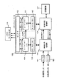
図1は、本発明の一実施形態による情報処理システムを適用した映像記録再生装置の構成例を示すブロック図である。
Hereinafter, embodiments of the present invention will be described with reference to the drawings.
FIG. 1 is a block diagram showing a configuration example of a video recording / reproducing apparatus to which an information processing system according to an embodiment of the present invention is applied.
A/D(アナログ・ディジタル)変換部101は、映像信号入力として入力されるアナログ映像信号をディジタル映像信号に変換する。D/A(ディジタル・アナログ)変換部102は、映像信号処理部103から供給されるディジタル映像信号をアナログ映像信号に変換し映像信号出力として出力する。
An A / D (analog / digital)
映像信号処理部103は、記録動作時において、A/D変換部101より供給されるディジタル映像信号を記録フォーマットに応じたデータフォーマットに変換し、記録再生処理部104へ記録映像データとして供給する。また、映像信号処理部103は、再生動作時において、記録再生処理部104より供給された再生映像データをディジタル映像信号に変換し、D/A変換部102へ供給する。
The video
記録再生処理部104は、記録動作時において、映像信号処理部103より供給された記録映像データを記録媒体107へ記録する。このとき、記録再生処理部104は、映像信号処理部103より供給された記録映像データに対して記録フォーマットに応じた符号化処理を行い、さらに誤り訂正符号を付加して記録媒体107への記録を行う。また、記録再生処理部104は、再生動作時において、記録媒体107から読み出されたデータに対して復号化処理及び誤り訂正処理を施し、復号化したデータを再生映像データとして映像信号処理部103に供給する。
The recording /
映像信号処理部103及び記録再生処理部104によって行われる処理は、それぞれメモリコントローラ105を介してメモリ106に対する所定のデータ長単位でデータの読み出し及び書き込みを行いながら実行される。メモリ106は、例えばSDRAM(Synchronous Dynamic Random Access Memory)であり、映像信号処理部103がアクセスする領域と記録再生処理部104がアクセスする領域は異なるバンクに配置されている。
The processing performed by the video
メモリコントローラ105は、FIFO(First In First Out)(A)108、シーケンサー(A)109、FIFO(B)110、シーケンサー(B)111、及びセレクタ部112で構成されている。
The
FIFO(A)108は、映像信号処理部103からの書き込みデータ又はメモリ106からの読み出しデータを一時的に保持し、シーケンサー(A)109は、映像信号処理部103からのメモリアクセス要求を制御する。同様に、FIFO(B)110は、記録再生処理部104からの書き込みデータ又はメモリ106からの読み出しデータを一時的に保持し、シーケンサー(B)111は、記録再生処理部104からのメモリアクセス要求を制御する。セレクタ部112は、シーケンサー(A)109及びシーケンサー(B)111からのSDRAMコマンド、アドレス及びデータを切り替える。
A FIFO (A) 108 temporarily holds write data from the video
ここで、シーケンサー(A)109は、映像信号処理部103から要求されたデータ長でのデータ転送を指定データ長単位に分割して、メモリ106との間でデータ転送を行うように制御する。同様に、シーケンサー(B)111は、記録再生処理部104から要求されたデータ長でのデータ転送を指定データ長単位に分割して、メモリ106との間でデータ転送を行うように制御する。
Here, the sequencer (A) 109 controls the data transfer with the data length requested from the video
シーケンサー(A)109は、メモリ106との間でデータ転送を行う際に、シーケンサー(B)111とメモリ106との間でのデータ転送に必要な時間間隔を空けてデータ転送を行うように動作する。すなわち、シーケンサー(A)109とメモリ106との間でのデータ転送では、指定データ長の分割データが転送され、少なくともシーケンサー(B)111とメモリ106との間でデータ転送を実行可能な時間が経過した後に、次の分割データが転送される。
The sequencer (A) 109 operates to perform data transfer with a time interval necessary for data transfer between the sequencer (B) 111 and the
また、シーケンサー(A)109は、シーケンサー(B)111の転送開始タイミング信号をシーケンサー(B)111へ供給している。シーケンサー(B)111は、シーケンサー(A)109から供給された転送開始タイミング信号に従ってメモリ106との間でのデータ転送を行うように動作する。つまり、この転送開始タイミング信号は、シーケンサー(B)111とメモリ106との間でのデータ転送の開始を許可する旨を示す信号である。
The sequencer (A) 109 supplies the transfer start timing signal of the sequencer (B) 111 to the sequencer (B) 111. The sequencer (B) 111 operates to transfer data to and from the
これにより、メモリコントローラ105は、映像信号処理部103及び記録再生処理部104からのメモリアクセス要求に応じてメモリ106に対するデータの読み書きを分割して行う。つまり、映像信号処理部103及び記録再生処理部104から要求されるメモリ106との間でのデータ転送は、メモリコントローラ105により時分割に分割されて行われる。
As a result, the
ここで、映像信号処理部103は、その内部に少なくとも映像信号1ライン分以下の処理に必要なデータ量を格納可能なメモリしか備えておらず、入出力を行う映像信号の1ライン時間内に1ライン分のデータをメモリ106へ読み書きする必要がある。映像信号処理部103は、映像信号1ラインに相当するデータを所定のデータ長単位でメモリ106へバースト転送を行うことでリアルタイム性を確保している。
Here, the video
それに対して、記録再生処理部104は、記録・再生処理動作時ともに映像信号の1フレーム時間内に1フレーム分のデータを処理すれば良い処理部である。すなわち、記録再生処理部104は、映像信号処理部103と比較してリアルタイム性が低く、また符号化されたデータを扱うために伝送レートも低い。なお、映像信号処理部103及び記録再生処理部104は、それぞれの処理タイミングで独立に所定のデータ長単位でデータ転送するためのメモリアクセス要求を行うことが可能である。
On the other hand, the recording /
なお、図1に示した各機能部(例えば、映像信号処理部103、記録再生処理部104、メモリコントローラ105、及びメモリ106)は、それぞれが独立したデバイスにより構成されていても良いし、集積化された1つのデバイスであっても良い。また、すべての機能部ではなく、任意の機能部が集積化されて1つのデバイスとして構成されていても良い。
Note that each function unit (for example, the video
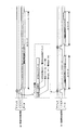
以下に、メモリコントローラ105におけるデータ転送制御動作について説明する。映像信号処理部103が、図2(a)に示すように90ワード長での読み出し要求を行い、記録再生処理部104が、図2(b)に示すように20ワード長での書き込み要求を行う場合を一例として説明する。なお、映像信号処理部103及び記録再生処理部104がメモリ106に対する読み出し要求や書き込み要求を行う際のデータ長は、これに限定されるものではなく任意である。
The data transfer control operation in the
ここで、映像信号処理部103及び記録再生処理部104は、それぞれ同様のプロトコルでメモリコントローラ105と通信を行う。すなわち、図2(a)、(b)に示すように、映像信号処理部103及び記録再生処理部104は、メモリ106との間でのデータ転送要求を示すリクエスト信号をハイレベルにアサートした区間に転送要求に係る内容を示すアドレス信号を同時に送信する。このリクエスト信号のアサート・タイミングから一定の期間が経過したタイミングで書き込みデータの出力、又は読み出しデータの入力を行うようになっている。
Here, the video
アドレス信号は、図2中に示されるように、R/W領域、バースト長領域、及びオフセットアドレス領域で定義されている。R/W領域は、その転送要求が読み出し要求であるか書き込み要求であるかを示し、バースト長領域は、転送データ量を示す。また、オフセットアドレス領域は、読み出し又は書き込みを行うメモリ106上の先頭アドレスを示す。メモリコントローラ105は、このアドレス信号における各情報に基づいてメモリ106との間でのデータ転送を行う。
As shown in FIG. 2, the address signal is defined by an R / W area, a burst length area, and an offset address area. The R / W area indicates whether the transfer request is a read request or a write request, and the burst length area indicates the amount of transfer data. The offset address area indicates the head address on the
まず、映像信号処理部103からの要求に係るデータ転送において、シーケンサー(A)109は、映像信号処理部103から要求されたバースト長を8ワード単位に分割するよう設定されている。また、バースト長が8ワード単位で割り切れない場合、その余りとなる端数ワード分は先頭のバースト長に加算して転送が行われるようにスケジューリングされる(これにより分割転送数が1回分軽減されるため、SDRAMコマンドにより発生するオーバーヘッドを軽減可能となっている)。
First, in the data transfer related to the request from the video
つまり、図2(a)に示した例では映像信号処理部103からの要求に係る90ワードを8ワード単位に分割するため、余りの2ワードが先頭に加算されて、10ワード(=8+2)×1回+8ワード×10回でデータ転送を行うようにスケジューリングされる。シーケンサー(A)109は、1分割転送毎(10ワード又は8ワードのデータ転送毎)に後述するシーケンサー(B)111による分割転送(後述する)に必要な時間間隔を空けてメモリ106との間でのデータ転送を行う。また、シーケンサー(A)109は、1分割転送(10ワード又は8ワードのデータ転送)が終了する度に、シーケンサー(B)111が分割転送を開始するための転送開始タイミング信号を生成してシーケンサー(B)111に供給している(図3(a)参照)。
That is, in the example shown in FIG. 2A, 90 words related to the request from the video
一方、記録再生処理部104からの要求に係るデータ転送において、シーケンサー(B)111は、記録再生処理部104から要求されたバースト長を4ワード単位に分割するよう設定されている。なお、バースト長が4ワード単位で割り切れない場合には、その余りとなる端数ワード分は先頭のバースト長に加算して転送が行われるようにスケジューリングされる。
On the other hand, in the data transfer related to the request from the recording /
図2(b)に示した例では記録再生処理部104からの要求に係る20ワードを4ワード単位に分割するため、4ワード×5回でデータ転送が行われるようにスケジューリングされる。メモリ106に対して書き込みを行う際には、記録再生処理部104から出力されたデータ(20ワード分)がFIFO(B)110に順次格納される。そして、シーケンサー(B)111は、シーケンサー(A)109から供給された転送開始タイミング信号に従って4ワードずつFIFO(B)110からデータを読み出し、メモリ106に対して書き込み転送を行う(図3(b)参照)。故に前述のシーケンサー(A)108によって設けられるシーケンサー(B)110での分割転送に要する空き間隔は、4ワード転送分の間隔となっている。
In the example shown in FIG. 2B, since 20 words related to the request from the recording /
シーケンサー(A)109及びシーケンサー(B)111と、メモリ106との間で入出力されるSDRAMコマンド、アドレス及びデータは、セレクタ部112により適宜切り替えられる。これにより、映像信号処理部103及び記録再生処理部104からそれぞれ要求されるデータ転送が時分割に分割されてメモリ106(SDRAM)との間でデータ転送が行われる(図3(c)参照)。ここで、シーケンサー(A)109に映像信号処理部103からのデータ転送要求がない場合には、シーケンサー(A)109は、シーケンサー(B)111のバースト転送に必要な最短間隔で転送開始タイミング信号を出力するようになっている(図4参照)。こうすることで、映像信号処理部103からデータ転送要求がなく、記録再生処理部104から要求されるデータ転送に競合がない場合には、記録再生処理部104の転送が効率的に行えるようになっている。
The SDRAM command, address, and data input / output between the sequencer (A) 109 and the sequencer (B) 111 and the
また、映像信号処理部103がアクセスする領域と記録再生処理部104がアクセスする領域は、上述したようにそれぞれメモリ106上で異なるバンクに配置されている。このように構成することで、図3(c)に示すように映像信号処理部103及び記録再生処理部104が交互にデータ転送を行う場合には、SDRAMのマルチバンクアクセスが可能となり、より効率的なデータ転送が行える。
The area accessed by the video
上述したデータ転送制御動作は、映像信号処理部103及び記録再生処理部104からの転送要求がそれぞれ他のバースト長での要求であったり、読み出し又は書き込みのどちらの要求であったりしても同様である。このデータ転送制御動作により、映像信号処理部103によるデータ転送を待たせることなく、映像信号処理部103及び記録再生処理部104による分割転送を同時に行うことが可能である。
The above-described data transfer control operation is the same regardless of whether the transfer request from the video
以上のように本実施形態によれば、映像信号処理部103及び記録再生処理部104から要求されるデータ転送を予め指定した固定データ長に分割してメモリ106との間でのデータ転送を行う。このとき、記録再生処理部104に係る分割した固定データ長でのデータ転送が実行可能な時間を分割データ転送後に空けるようにして映像信号処理部103に係る分割した固定データ長でのデータ転送を行う。そして、記録再生処理部104に係るデータ転送をその空き時間で行う。このように容易な制御で時分割転送を行うことにより、映像信号処理部103に係るデータ転送を待たせることなく、ほぼ同時に記録再生処理部104に係るデータ転送を行うことが可能になる。したがって、映像信号処理部103及び記録再生処理部104と、それらが共通して用いるメモリ106との間での効率的なメモリ転送ができ、容易にかつリアルタイム性等を破綻することなくデータ転送を行うことが可能になる。
As described above, according to the present embodiment, data transfer requested from the video
なお、上記実施形態は、何れも本発明を実施するにあたっての具体化のほんの一例を示したものに過ぎず、これらによって本発明の技術的範囲が限定的に解釈されてはならないものである。すなわち、本発明はその技術思想、またはその主要な特徴から逸脱することなく、様々な形で実施することができる。 The above-described embodiments are merely examples of implementation in carrying out the present invention, and the technical scope of the present invention should not be construed as being limited thereto. That is, the present invention can be implemented in various forms without departing from the technical idea or the main features thereof.
103 映像信号処理部
104 記録再生処理部
105 メモリコントローラ
106 メモリ
107 記録媒体
108、110 FIFO
109、111 シーケンサー
112 セレクタ部
103 video
109, 111
Claims (10)
前記複数の処理手段とメモリとの間のデータ転送を制御する手段であって、前記複数の処理手段における第1の処理手段から転送要求された第1のデータを第1のデータ長を単位として転送し、前記複数の処理手段における第2の処理手段から転送要求された第2のデータを前記第1のデータ長よりも短い第2のデータ長を単位として転送する制御手段とを備え、
前記制御手段は、前記第1のデータ長の第1のデータを転送した後、一つの前記第2のデータ長の第2のデータを転送するために必要な時間間隔で、次の前記第1のデータ長の第1のデータを転送し、前記第1のデータ長の第1のデータを転送した後に次の前記第1のデータ長の第1のデータを転送するまでの間に前記第2のデータ長の第2のデータを転送することを特徴とするメモリ制御装置。 A plurality of processing means;
Means for controlling data transfer between the plurality of processing means and the memory, wherein the first data requested to be transferred from the first processing means in the plurality of processing means is expressed in units of a first data length. Control means for transferring and transferring the second data requested to be transferred from the second processing means in the plurality of processing means in units of a second data length shorter than the first data length;
The control means transfers the next first data at a time interval necessary for transferring the second data having one second data length after transferring the first data having the first data length. The first data having the data length of the first data length is transferred, and the second data is transferred between the transfer of the first data having the first data length and the transfer of the first data having the first data length. A memory control device for transferring second data having a data length of.
前記第1の転送制御部は、前記第1のデータ長の第1のデータの転送が終了したことに応じて、前記第2の転送制御部に転送許可を出力し、
前記第2の転送制御部は、前記第1の転送制御部からの前記転送許可に応じて前記第2のデータ長の第2のデータを転送することを特徴とする請求項1に記載のメモリ制御装置。 The control means includes a first transfer control unit that controls transfer of the first data, and a second transfer control unit that controls transfer of the second data,
The first transfer control unit outputs transfer permission to the second transfer control unit in response to completion of transfer of the first data of the first data length,
2. The memory according to claim 1, wherein the second transfer control unit transfers the second data having the second data length in accordance with the transfer permission from the first transfer control unit. Control device.
前記複数の処理手段における第1の処理手段から転送要求された第1のデータを第1のデータ長を単位として転送し、前記複数の処理手段における第2の処理手段から転送要求された第2のデータを前記第1のデータ長よりも短い第2のデータ長を単位として転送し、前記第1のデータ長の第1のデータを転送した後、一つの前記第2のデータ長の第2のデータを転送するために必要な時間間隔で、次の前記第1のデータ長の第1のデータを転送し、前記第1のデータ長の第1のデータを転送した後に次の前記第1のデータ長の第1のデータを転送するまでの間に前記第2のデータ長の第2のデータを転送することを特徴とするメモリ制御方法。 A method for controlling data transfer between a memory and a plurality of processing means,
The first data requested to be transferred from the first processing means in the plurality of processing means is transferred in units of a first data length, and the second data requested to be transferred from the second processing means in the plurality of processing means. Is transferred in units of a second data length shorter than the first data length, the first data of the first data length is transferred, and then the second data length of one second data length is transferred. The first data having the first data length is transferred at a time interval necessary for transferring the first data, and the first data having the first data length is transferred and then the first data having the first data length is transferred. A memory control method comprising: transferring the second data having the second data length before the first data having the data length is transferred.
Priority Applications (1)
| Application Number | Priority Date | Filing Date | Title |
|---|---|---|---|
| JP2005346892A JP5037814B2 (en) | 2005-11-30 | 2005-11-30 | Memory control device and memory control method |
Applications Claiming Priority (1)
| Application Number | Priority Date | Filing Date | Title |
|---|---|---|---|
| JP2005346892A JP5037814B2 (en) | 2005-11-30 | 2005-11-30 | Memory control device and memory control method |
Publications (2)
| Publication Number | Publication Date |
|---|---|
| JP2007156544A JP2007156544A (en) | 2007-06-21 |
| JP5037814B2 true JP5037814B2 (en) | 2012-10-03 |
Family
ID=38240872
Family Applications (1)
| Application Number | Title | Priority Date | Filing Date |
|---|---|---|---|
| JP2005346892A Expired - Fee Related JP5037814B2 (en) | 2005-11-30 | 2005-11-30 | Memory control device and memory control method |
Country Status (1)
| Country | Link |
|---|---|
| JP (1) | JP5037814B2 (en) |
Families Citing this family (1)
| Publication number | Priority date | Publication date | Assignee | Title |
|---|---|---|---|---|
| JP7419010B2 (en) * | 2019-10-04 | 2024-01-22 | キヤノン株式会社 | Data processing systems and methods of controlling data processing systems |
Family Cites Families (4)
| Publication number | Priority date | Publication date | Assignee | Title |
|---|---|---|---|---|
| JPS56152064A (en) * | 1980-04-23 | 1981-11-25 | Mitsubishi Electric Corp | Data transfer device |
| JPH09297705A (en) * | 1996-05-08 | 1997-11-18 | Sony Corp | Memory control method |
| FR2769727B1 (en) * | 1997-10-09 | 2000-01-28 | St Microelectronics Sa | METHOD AND SYSTEM FOR CONTROLLING SHARED ACCESS TO A RAM |
| JP2001296973A (en) * | 2000-04-12 | 2001-10-26 | Fuji Xerox Co Ltd | System and method for accessing storage device |
-
2005
- 2005-11-30 JP JP2005346892A patent/JP5037814B2/en not_active Expired - Fee Related
Also Published As
| Publication number | Publication date |
|---|---|
| JP2007156544A (en) | 2007-06-21 |
Similar Documents
| Publication | Publication Date | Title |
|---|---|---|
| JP4408263B2 (en) | Data transfer system and data transfer method | |
| US20030088743A1 (en) | Mobile wireless communication device architectures and methods therefor | |
| JP2006318139A (en) | Data transfer device, data transfer method and program | |
| JP2009015832A (en) | Inter-access arbitration circuit, semiconductor device, and inter-access arbitration method | |
| JP2006195714A (en) | Resource management device | |
| JP2006259898A (en) | I/o controller, signal processing system and data transferring method | |
| JP2007249938A (en) | Usb host system, av data reproducing device and av data recording device | |
| JP5037814B2 (en) | Memory control device and memory control method | |
| JP2007172254A (en) | Memory control circuit | |
| JP2007299237A (en) | Information transfer device, and information transfer method | |
| AU5248300A (en) | Data transfer apparatus, data transfer system, and data transfer method with double buffering | |
| EP2183663B1 (en) | Mass storage system with improved usage of buffer capacity | |
| US20060041690A1 (en) | Software communication between MPEG layer and servo layer | |
| JP5146284B2 (en) | Data transfer apparatus and data transfer method | |
| US20100146158A1 (en) | Data processing circuit | |
| JP2005063358A (en) | Instruction supply controller and semiconductor device | |
| JP4023332B2 (en) | Recording / playback device | |
| JP2008269348A (en) | Memory control device and memory control method | |
| JP2004086439A (en) | Data recording/reproducing device, and data read/write control method to its hard disk drive | |
| JP4257656B2 (en) | Audio data processing device | |
| JP6124615B2 (en) | MEMORY CONTROL DEVICE, MEMORY CONTROL METHOD, AND IMAGING DEVICE HAVING MEMORY CONTROL DEVICE | |
| JP2002091823A (en) | Memory controller to be used for image display device | |
| JP2712414B2 (en) | Image storage circuit | |
| JP2001035078A (en) | Data recording and reproducing device and data transferring method therefor | |
| JP2009169599A (en) | Bus device |
Legal Events
| Date | Code | Title | Description |
|---|---|---|---|
| A621 | Written request for application examination |
Free format text: JAPANESE INTERMEDIATE CODE: A621 Effective date: 20081125 |
|
| A977 | Report on retrieval |
Free format text: JAPANESE INTERMEDIATE CODE: A971007 Effective date: 20110728 |
|
| A131 | Notification of reasons for refusal |
Free format text: JAPANESE INTERMEDIATE CODE: A131 Effective date: 20110809 |
|
| A521 | Request for written amendment filed |
Free format text: JAPANESE INTERMEDIATE CODE: A523 Effective date: 20111007 |
|
| A131 | Notification of reasons for refusal |
Free format text: JAPANESE INTERMEDIATE CODE: A131 Effective date: 20120221 |
|
| A521 | Request for written amendment filed |
Free format text: JAPANESE INTERMEDIATE CODE: A523 Effective date: 20120419 |
|
| TRDD | Decision of grant or rejection written | ||
| A01 | Written decision to grant a patent or to grant a registration (utility model) |
Free format text: JAPANESE INTERMEDIATE CODE: A01 Effective date: 20120703 |
|
| A01 | Written decision to grant a patent or to grant a registration (utility model) |
Free format text: JAPANESE INTERMEDIATE CODE: A01 |
|
| A61 | First payment of annual fees (during grant procedure) |
Free format text: JAPANESE INTERMEDIATE CODE: A61 Effective date: 20120705 |
|
| FPAY | Renewal fee payment (event date is renewal date of database) |
Free format text: PAYMENT UNTIL: 20150713 Year of fee payment: 3 |
|
| R151 | Written notification of patent or utility model registration |
Ref document number: 5037814 Country of ref document: JP Free format text: JAPANESE INTERMEDIATE CODE: R151 |
|
| FPAY | Renewal fee payment (event date is renewal date of database) |
Free format text: PAYMENT UNTIL: 20150713 Year of fee payment: 3 |
|
| LAPS | Cancellation because of no payment of annual fees |